EP4372808A2 - Halbleiterbauelement mit verstärktem dielektrikum und verfahren dafür - Google Patents
Halbleiterbauelement mit verstärktem dielektrikum und verfahren dafür Download PDFInfo
- Publication number
- EP4372808A2 EP4372808A2 EP23198515.1A EP23198515A EP4372808A2 EP 4372808 A2 EP4372808 A2 EP 4372808A2 EP 23198515 A EP23198515 A EP 23198515A EP 4372808 A2 EP4372808 A2 EP 4372808A2
- Authority
- EP
- European Patent Office
- Prior art keywords
- conductive layer
- rdl
- metal layer
- layer
- plateau
- Prior art date
- Legal status (The legal status is an assumption and is not a legal conclusion. Google has not performed a legal analysis and makes no representation as to the accuracy of the status listed.)
- Withdrawn
Links
Images




Classifications
-
- H—ELECTRICITY
- H10—SEMICONDUCTOR DEVICES; ELECTRIC SOLID-STATE DEVICES NOT OTHERWISE PROVIDED FOR
- H10W—GENERIC PACKAGES, INTERCONNECTIONS, CONNECTORS OR OTHER CONSTRUCTIONAL DETAILS OF DEVICES COVERED BY CLASS H10
- H10W70/00—Package substrates; Interposers; Redistribution layers [RDL]
- H10W70/01—Manufacture or treatment
- H10W70/05—Manufacture or treatment of insulating or insulated package substrates, or of interposers, or of redistribution layers
- H10W70/08—Manufacture or treatment of insulating or insulated package substrates, or of interposers, or of redistribution layers by depositing layers on the chip or wafer, e.g. "chip-first" RDLs
- H10W70/09—Manufacture or treatment of insulating or insulated package substrates, or of interposers, or of redistribution layers by depositing layers on the chip or wafer, e.g. "chip-first" RDLs extending onto an encapsulation that laterally surrounds the chip or wafer, e.g. fan-out wafer level package [FOWLP] RDLs
-
- H—ELECTRICITY
- H10—SEMICONDUCTOR DEVICES; ELECTRIC SOLID-STATE DEVICES NOT OTHERWISE PROVIDED FOR
- H10W—GENERIC PACKAGES, INTERCONNECTIONS, CONNECTORS OR OTHER CONSTRUCTIONAL DETAILS OF DEVICES COVERED BY CLASS H10
- H10W74/00—Encapsulations, e.g. protective coatings
- H10W74/10—Encapsulations, e.g. protective coatings characterised by their shape or disposition
- H10W74/111—Encapsulations, e.g. protective coatings characterised by their shape or disposition the semiconductor body being completely enclosed
- H10W74/114—Encapsulations, e.g. protective coatings characterised by their shape or disposition the semiconductor body being completely enclosed by a substrate and the encapsulations
- H10W74/117—Encapsulations, e.g. protective coatings characterised by their shape or disposition the semiconductor body being completely enclosed by a substrate and the encapsulations the substrate having spherical bumps for external connection
-
- H—ELECTRICITY
- H10—SEMICONDUCTOR DEVICES; ELECTRIC SOLID-STATE DEVICES NOT OTHERWISE PROVIDED FOR
- H10W—GENERIC PACKAGES, INTERCONNECTIONS, CONNECTORS OR OTHER CONSTRUCTIONAL DETAILS OF DEVICES COVERED BY CLASS H10
- H10W42/00—Arrangements for protection of devices
-
- H—ELECTRICITY
- H10—SEMICONDUCTOR DEVICES; ELECTRIC SOLID-STATE DEVICES NOT OTHERWISE PROVIDED FOR
- H10W—GENERIC PACKAGES, INTERCONNECTIONS, CONNECTORS OR OTHER CONSTRUCTIONAL DETAILS OF DEVICES COVERED BY CLASS H10
- H10W42/00—Arrangements for protection of devices
- H10W42/121—Arrangements for protection of devices protecting against mechanical damage
-
- H—ELECTRICITY
- H10—SEMICONDUCTOR DEVICES; ELECTRIC SOLID-STATE DEVICES NOT OTHERWISE PROVIDED FOR
- H10W—GENERIC PACKAGES, INTERCONNECTIONS, CONNECTORS OR OTHER CONSTRUCTIONAL DETAILS OF DEVICES COVERED BY CLASS H10
- H10W72/00—Interconnections or connectors in packages
- H10W72/01—Manufacture or treatment
- H10W72/012—Manufacture or treatment of bump connectors, dummy bumps or thermal bumps
-
- H—ELECTRICITY
- H10—SEMICONDUCTOR DEVICES; ELECTRIC SOLID-STATE DEVICES NOT OTHERWISE PROVIDED FOR
- H10W—GENERIC PACKAGES, INTERCONNECTIONS, CONNECTORS OR OTHER CONSTRUCTIONAL DETAILS OF DEVICES COVERED BY CLASS H10
- H10W72/00—Interconnections or connectors in packages
- H10W72/01—Manufacture or treatment
- H10W72/019—Manufacture or treatment of bond pads
-
- H—ELECTRICITY
- H10—SEMICONDUCTOR DEVICES; ELECTRIC SOLID-STATE DEVICES NOT OTHERWISE PROVIDED FOR
- H10W—GENERIC PACKAGES, INTERCONNECTIONS, CONNECTORS OR OTHER CONSTRUCTIONAL DETAILS OF DEVICES COVERED BY CLASS H10
- H10W72/00—Interconnections or connectors in packages
- H10W72/851—Dispositions of multiple connectors or interconnections
-
- H—ELECTRICITY
- H10—SEMICONDUCTOR DEVICES; ELECTRIC SOLID-STATE DEVICES NOT OTHERWISE PROVIDED FOR
- H10W—GENERIC PACKAGES, INTERCONNECTIONS, CONNECTORS OR OTHER CONSTRUCTIONAL DETAILS OF DEVICES COVERED BY CLASS H10
- H10W72/00—Interconnections or connectors in packages
- H10W72/90—Bond pads, in general
-
- H—ELECTRICITY
- H10—SEMICONDUCTOR DEVICES; ELECTRIC SOLID-STATE DEVICES NOT OTHERWISE PROVIDED FOR
- H10W—GENERIC PACKAGES, INTERCONNECTIONS, CONNECTORS OR OTHER CONSTRUCTIONAL DETAILS OF DEVICES COVERED BY CLASS H10
- H10W74/00—Encapsulations, e.g. protective coatings
- H10W74/10—Encapsulations, e.g. protective coatings characterised by their shape or disposition
- H10W74/131—Encapsulations, e.g. protective coatings characterised by their shape or disposition the semiconductor body being only partially enclosed
-
- H—ELECTRICITY
- H10—SEMICONDUCTOR DEVICES; ELECTRIC SOLID-STATE DEVICES NOT OTHERWISE PROVIDED FOR
- H10W—GENERIC PACKAGES, INTERCONNECTIONS, CONNECTORS OR OTHER CONSTRUCTIONAL DETAILS OF DEVICES COVERED BY CLASS H10
- H10W74/00—Encapsulations, e.g. protective coatings
- H10W74/10—Encapsulations, e.g. protective coatings characterised by their shape or disposition
- H10W74/131—Encapsulations, e.g. protective coatings characterised by their shape or disposition the semiconductor body being only partially enclosed
- H10W74/147—Encapsulations, e.g. protective coatings characterised by their shape or disposition the semiconductor body being only partially enclosed the encapsulations being multilayered
-
- H—ELECTRICITY
- H10—SEMICONDUCTOR DEVICES; ELECTRIC SOLID-STATE DEVICES NOT OTHERWISE PROVIDED FOR
- H10W—GENERIC PACKAGES, INTERCONNECTIONS, CONNECTORS OR OTHER CONSTRUCTIONAL DETAILS OF DEVICES COVERED BY CLASS H10
- H10W70/00—Package substrates; Interposers; Redistribution layers [RDL]
- H10W70/01—Manufacture or treatment
- H10W70/05—Manufacture or treatment of insulating or insulated package substrates, or of interposers, or of redistribution layers
-
- H—ELECTRICITY
- H10—SEMICONDUCTOR DEVICES; ELECTRIC SOLID-STATE DEVICES NOT OTHERWISE PROVIDED FOR
- H10W—GENERIC PACKAGES, INTERCONNECTIONS, CONNECTORS OR OTHER CONSTRUCTIONAL DETAILS OF DEVICES COVERED BY CLASS H10
- H10W70/00—Package substrates; Interposers; Redistribution layers [RDL]
- H10W70/60—Insulating or insulated package substrates; Interposers; Redistribution layers
-
- H—ELECTRICITY
- H10—SEMICONDUCTOR DEVICES; ELECTRIC SOLID-STATE DEVICES NOT OTHERWISE PROVIDED FOR
- H10W—GENERIC PACKAGES, INTERCONNECTIONS, CONNECTORS OR OTHER CONSTRUCTIONAL DETAILS OF DEVICES COVERED BY CLASS H10
- H10W70/00—Package substrates; Interposers; Redistribution layers [RDL]
- H10W70/60—Insulating or insulated package substrates; Interposers; Redistribution layers
- H10W70/62—Insulating or insulated package substrates; Interposers; Redistribution layers characterised by their interconnections
- H10W70/65—Shapes or dispositions of interconnections
- H10W70/652—Cross-sectional shapes
- H10W70/6528—Cross-sectional shapes of the portions that connect to chips, wafers or package parts
-
- H—ELECTRICITY
- H10—SEMICONDUCTOR DEVICES; ELECTRIC SOLID-STATE DEVICES NOT OTHERWISE PROVIDED FOR
- H10W—GENERIC PACKAGES, INTERCONNECTIONS, CONNECTORS OR OTHER CONSTRUCTIONAL DETAILS OF DEVICES COVERED BY CLASS H10
- H10W70/00—Package substrates; Interposers; Redistribution layers [RDL]
- H10W70/60—Insulating or insulated package substrates; Interposers; Redistribution layers
- H10W70/62—Insulating or insulated package substrates; Interposers; Redistribution layers characterised by their interconnections
- H10W70/65—Shapes or dispositions of interconnections
- H10W70/654—Top-view layouts
-
- H—ELECTRICITY
- H10—SEMICONDUCTOR DEVICES; ELECTRIC SOLID-STATE DEVICES NOT OTHERWISE PROVIDED FOR
- H10W—GENERIC PACKAGES, INTERCONNECTIONS, CONNECTORS OR OTHER CONSTRUCTIONAL DETAILS OF DEVICES COVERED BY CLASS H10
- H10W72/00—Interconnections or connectors in packages
- H10W72/20—Bump connectors, e.g. solder bumps or copper pillars; Dummy bumps; Thermal bumps
-
- H—ELECTRICITY
- H10—SEMICONDUCTOR DEVICES; ELECTRIC SOLID-STATE DEVICES NOT OTHERWISE PROVIDED FOR
- H10W—GENERIC PACKAGES, INTERCONNECTIONS, CONNECTORS OR OTHER CONSTRUCTIONAL DETAILS OF DEVICES COVERED BY CLASS H10
- H10W72/00—Interconnections or connectors in packages
- H10W72/20—Bump connectors, e.g. solder bumps or copper pillars; Dummy bumps; Thermal bumps
- H10W72/221—Structures or relative sizes
-
- H—ELECTRICITY
- H10—SEMICONDUCTOR DEVICES; ELECTRIC SOLID-STATE DEVICES NOT OTHERWISE PROVIDED FOR
- H10W—GENERIC PACKAGES, INTERCONNECTIONS, CONNECTORS OR OTHER CONSTRUCTIONAL DETAILS OF DEVICES COVERED BY CLASS H10
- H10W72/00—Interconnections or connectors in packages
- H10W72/20—Bump connectors, e.g. solder bumps or copper pillars; Dummy bumps; Thermal bumps
- H10W72/231—Shapes
- H10W72/232—Plan-view shape, i.e. in top view
-
- H—ELECTRICITY
- H10—SEMICONDUCTOR DEVICES; ELECTRIC SOLID-STATE DEVICES NOT OTHERWISE PROVIDED FOR
- H10W—GENERIC PACKAGES, INTERCONNECTIONS, CONNECTORS OR OTHER CONSTRUCTIONAL DETAILS OF DEVICES COVERED BY CLASS H10
- H10W72/00—Interconnections or connectors in packages
- H10W72/20—Bump connectors, e.g. solder bumps or copper pillars; Dummy bumps; Thermal bumps
- H10W72/241—Dispositions, e.g. layouts
- H10W72/244—Dispositions, e.g. layouts relative to underlying supporting features, e.g. bond pads, RDLs or vias
-
- H—ELECTRICITY
- H10—SEMICONDUCTOR DEVICES; ELECTRIC SOLID-STATE DEVICES NOT OTHERWISE PROVIDED FOR
- H10W—GENERIC PACKAGES, INTERCONNECTIONS, CONNECTORS OR OTHER CONSTRUCTIONAL DETAILS OF DEVICES COVERED BY CLASS H10
- H10W72/00—Interconnections or connectors in packages
- H10W72/20—Bump connectors, e.g. solder bumps or copper pillars; Dummy bumps; Thermal bumps
- H10W72/29—Bond pads specially adapted therefor
-
- H—ELECTRICITY
- H10—SEMICONDUCTOR DEVICES; ELECTRIC SOLID-STATE DEVICES NOT OTHERWISE PROVIDED FOR
- H10W—GENERIC PACKAGES, INTERCONNECTIONS, CONNECTORS OR OTHER CONSTRUCTIONAL DETAILS OF DEVICES COVERED BY CLASS H10
- H10W72/00—Interconnections or connectors in packages
- H10W72/851—Dispositions of multiple connectors or interconnections
- H10W72/853—On the same surface
-
- H—ELECTRICITY
- H10—SEMICONDUCTOR DEVICES; ELECTRIC SOLID-STATE DEVICES NOT OTHERWISE PROVIDED FOR
- H10W—GENERIC PACKAGES, INTERCONNECTIONS, CONNECTORS OR OTHER CONSTRUCTIONAL DETAILS OF DEVICES COVERED BY CLASS H10
- H10W74/00—Encapsulations, e.g. protective coatings
- H10W74/10—Encapsulations, e.g. protective coatings characterised by their shape or disposition
- H10W74/111—Encapsulations, e.g. protective coatings characterised by their shape or disposition the semiconductor body being completely enclosed
- H10W74/129—Encapsulations, e.g. protective coatings characterised by their shape or disposition the semiconductor body being completely enclosed forming a chip-scale package [CSP]
Definitions
- This disclosure relates generally to semiconductor device packaging, and more specifically, to a semiconductor device with reinforced dielectric and method of forming the same.
- semiconductor device packaging with a reinforced dielectric structure.
- the semiconductor device packaging includes a redistribution layer formed over a semiconductor die and connected to die pads of the semiconductor die.
- a dielectric layer e.g., top non-conductive layer
- a plurality of openings is formed in the dielectric layer to expose respective portions of the underlying redistribution layer.
- the openings in the dielectric layer and corresponding exposed portions of the redistribution layer are configured for under-bump metallization structures formed at a subsequent stage of manufacturing.
- a shallow-etched cavity region is etched into a top surface of the dielectric layer such that a plurality of plateau regions of the dielectric layer are formed.
- Each plateau region of the plurality of the plateau regions is separated from one another by way of the cavity region.
- a metal layer is formed over the dielectric layer and exposed portions of the redistribution layer. Exposed portions of the metal layer are etched at a subsequent stage of manufacturing to expose top surfaces of the plurality of plateau regions. In this manner, the etched metal layer provides a frame-like structure interlocked with the dielectric layer surface.
- the interlocked metal layer with the dielectric layer serves to reinforced dielectric layer structure. Accordingly, the reinforced dielectric layer is significantly less susceptible to cracks, delamination, and degradation associated with adverse environmental conditions thus allowing for improved packaging integrity and reliability over the lifetime of the semiconductor device.
- FIG. 1 illustrates, in a simplified plan view, a portion of an example semiconductor device 100 having a reinforced dielectric structure in accordance with an embodiment.
- the device 100 includes an exposed portion of a final passivation layer 102 of a semiconductor die, a non-conductive layer formed over the final passivation layer 102, and a metal layer 104 formed over the non-conductive layer.
- the metal layer 104 is patterned and etched to form plateau regions 106 and 108 exposed through the metal layer 104.
- the metal layer 104 is configured to reinforce the underlying non-conductive layer and seal the outer edge of the non-conductive layer at the final passivation layer 102 of the semiconductor die.
- conductive connectors (e.g., solder balls) 110 are affixed to conductive under bump structures (not shown) formed over the semiconductor die.
- conductive connectors e.g., solder balls
- conductive under bump structures not shown
- conductive connectors 110 are affixed to conductive under bump structures (not shown) formed over the semiconductor die.
- conductive connectors e.g., solder balls
- conductive under bump structures not shown
- FIG. 2 through FIG. 10 illustrate, in simplified cross-sectional views, the example semiconductor device 100 taken along line A-A of FIG. 1 at various stages of manufacture in accordance with an embodiment.
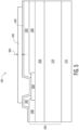
- FIG. 2 illustrates, in a simplified cross-sectional view, the example semiconductor device 100 at a stage of manufacture in accordance with an embodiment.
- a semiconductor die 202 is at least partially encapsulated with an encapsulant (e.g., epoxy molding compound) 212.
- the semiconductor die 202 includes a substrate region (e.g., bulk) 210, an active region (e.g., circuitry, interconnect) 206 formed at an active side of the semiconductor die, a die pad 204 conductively connected to the circuitry and/or interconnect of the active region, and a final passivation layer 208 formed over the active side of the semiconductor die.
- the semiconductor die 202 may be provided in a wafer form or portion of a wafer.
- the semiconductor die 202 may include any number of conductive interconnect layers and passivation layers.
- the die pad 204 at a top surface and the overlying final passivation layer 208 are depicted.
- the final passivation layer 208 depicted in FIG. 2 corresponds to the final passivation layer 102 depicted in FIG. 1 .
- the semiconductor die 202 is configured and arranged in an active side up orientation.
- the die pad 204 at the active side is configured for connection to printed circuit board (PCB) by way of a redistribution layer, under-bump structure, and conductive connectors formed at subsequent stages, for example.
- the semiconductor die 202 may be formed from any suitable semiconductor material, such as silicon, germanium, gallium arsenide, gallium nitride, silicon nitride, silicon carbide, and the like.
- the semiconductor die 202 may further include any digital circuits, analog circuits, RF circuits, memory, processor, MEMS, sensors, the like, and combinations thereof.
- FIG. 3 illustrates, in a simplified cross-sectional view, the example semiconductor device 100 at a subsequent stage of manufacture in accordance with an embodiment.
- a first non-conductive (e.g., dielectric) layer 302 is formed over the semiconductor die 202.
- the non-conductive layer 302 is deposited or otherwise applied on the top surface of the semiconductor die 202.
- the non-conductive layer 302 may be formed from suitable non-conducting materials such as polybenzoxazole (PBO), polyimide, Ajinomoto build-up film (ABF), and epoxy molding compound, for example.
- An opening 304 is formed in the non-conductive layer 302.
- the opening 304 is formed through the non-conductive layer 302 and located over the die pad 204 such that a substantial portion of a top surface of the die pad 204 is exposed.
- the opening 304 may be formed using techniques such as laser drilling, or etching, for example.
- an outer portion of the final passivation layer 208 near the outer edge of the semiconductor die 202 remains exposed (e.g., not covered with the non-conductive layer 302).
- FIG. 4 illustrates, in a simplified cross-sectional view, the example semiconductor device 100 at a subsequent stage of manufacture in accordance with an embodiment.
- a conductive redistribution layer (RDL) 402 is formed over the non-conductive layer 302 and exposed portion of the die pad 204.
- the term "conductive,” as used herein, generally refers to electrical conductivity unless otherwise specified.
- the RDL 402 may be formed by depositing a relatively thin seed layer (not shown), patterning, and utilizing the seed layer in a metal (e.g., copper) plating process, for example.
- the RDL 402 forms a conformal conductive layer on the exposed die pad 204 in the opening 304 and portions of the non-conductive 302 layer.
- the RDL 402 is conductively connected to the die pad 204 and configured to interconnect the die pad 204 with an under-bump structure formed at a subsequent stage, for example.
- FIG. 5 illustrates, in a simplified cross-sectional view, the example semiconductor device 100 at a subsequent stage of manufacture in accordance with an embodiment.
- a second non-conductive (e.g., dielectric) layer 502 is formed over the RDL 402 and the first non-conductive layer 302.
- the non-conductive layer 502 is deposited or otherwise applied on the RDL 402 and the exposed top surface of the non-conductive layer 302.
- the non-conductive layer 502 may be formed from suitable non-conducting materials such as PBO, polyimide, ABF, and epoxy molding compound, for example.
- non-conductive layer 502 may be characterized as a photo-imageable polymer material (e.g., photosensitive solder mask material) layer.
- An opening 504 and a shallow etched cavity region 506 are patterned and formed in the non-conductive layer 502.
- the opening 504 may be formed using traditional masking and exposure techniques and the cavity region 506 may be formed using known gray-scale masking and lensing exposure techniques to limit the depth of the cavity region, for example.
- the opening 504 and the cavity region 506 are patterned (e.g., masking, exposure) and etched during a same process operation. In other embodiments, the opening 504 may be formed in a process operation different from that of the cavity region 506 formation.
- the opening 504 is formed through the non-conductive layer 502 and located over a portion of the RDL 402 such that a portion of a top surface of the RDL 402 is exposed through the opening.
- the cavity region 506 is formed as a shallow etched region at a top surface of the non-conductive layer 502 and configured to form a plurality of plateau regions 508 and 510. A portion of the non-conductive layer 502 remains between the bottom surface of the cavity region 506 and a bottom surface of the non-conductive layer 502.
- the cavity region 506 is configured to have a predetermined depth dimension 512 measured from the top surface of the plateau regions 508 and 510 to the bottom surface of the cavity region 506.
- the predetermined depth dimension 512 is approximately in a range of 0.1 microns to 0.5 microns.
- the plateau regions 508 and 510 correspond to the respective plateau regions 106 and 108 depicted in FIG. 1 .
- the plateau region 508 is formed as a donut shape that substantially surrounds the opening 504.
- the plateau regions 510 are formed having a substantially round shape with a predetermined width (e.g., diameter) dimension 514 in a range of 5 microns to 50 microns.
- the plateau regions 510 may be formed having other shapes and/or width dimensions.
- an outer portion of the non-conductive layer 502 extends toward the outer perimeter of the semiconductor die and is configured to seal (e.g., enclose) an outer edge of the non-conductive layer 302 leaving an outer portion of the final passivation layer 208 exposed (e.g., not covered with the non-conductive layers 302 and 502) near the outer edge of the semiconductor die 202.
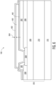
- FIG. 6 illustrates, in a simplified cross-sectional view, the example semiconductor device 100 at a subsequent stage of manufacture in accordance with an embodiment.
- a metal layer 602 and a seed layer 604 are formed over the patterned and etched non-conductive layer 502 and exposed portion of the RDL 402 in the opening 504.
- the metal layer 602 is characterized as anti-oxidation, corrosion resistant, high rigidity metal such as titanium, nickel-vanadium, zirconium, stainless steel, and alloys thereof.
- the metal layer 602 may be formed by sputtering, deposited, or otherwise applied over the non-conductive layer 502 and exposed portion of the RDL 402.
- the metal layer 602 is formed to have thickness sufficient to at least substantially fill the cavity region 506 of the non-conductive layer 502.
- the seed layer 604 is formed as a relatively thin layer and may include copper, tungsten, palladium, or suitable alloys thereof conducive for plating at a subsequent stage of manufacture, for example.
- FIG. 7 illustrates, in a simplified cross-sectional view, the example semiconductor device 100 at a subsequent stage of manufacture in accordance with an embodiment.
- a conductive under-bump metallization (UBM) 702 is formed on the seed layer 604.
- the UBM 702 includes copper and is formed by utilizing the seed layer 604 in a copper plating operation.
- the copper plating operation may be characterized as an electroless process or an electroplating process.
- the UBM 702 forms a conformal conductive layer over the exposed pad region and sidewalls of the cavity 504 ( FIG. 6 ).
- the UBM 702 is patterned and configured to interconnect the die pad 204 by way of the RDL 402. In other embodiments, the UBM 702 may be formed by plating other metal materials.
- FIG. 8 illustrates, in a simplified cross-sectional view, the example semiconductor device 100 at a subsequent stage of manufacture in accordance with an embodiment.
- the seed layer 604 is removed.
- the remaining exposed portions of the seed layer 604 is etched and removed.
- portions of the metal layer 602 underlying the seed layer 604 are exposed by way of removing the remaining exposed portions of the seed layer 604.
- FIG. 9 illustrates, in a simplified cross-sectional view, the example semiconductor device 100 at a subsequent stage of manufacture in accordance with an embodiment.
- exposed portions of the metal layer (602) are etched to reveal top surfaces of the respective plateau regions 508 and 510 of the non-conductive layer 502.
- the plateau regions 508 and 510 of the non-conductive layer 502 depicted in FIG. 9 corresponds to the plurality of plateau regions 106 and 108 depicted in FIG. 1 .
- the etched metal layer (602) leaves a first metal layer portion 902 substantially filled in the cavity region 506 and a second metal layer portion 904 disposed between the UBM 702 and the RDL 402.
- a top surface of the metal layer portion 902 is substantially coplanar with the top surface of the plateau regions 508 and 510.
- the metal layer portion 902 is configured to substantially reinforce the underlying non-conductive layers 502 and 302. With the plateau regions 508 and 510 exposed, the metal layer portion 902 is essentially interlocked with the non-conductive layer 502 and thus adding rigidity to the non-conductive layer 502.
- the metal layer portion 902 is further configured to seal the outer perimeter of the non-conductive layer 502.
- the adhesion properties of the metal layer portion 902 minimizes potential delamination associated with extreme environmental conditions (e.g., temperature, moisture, corrosion).
- the plateau regions 508 and 510 of the non-conductive layer 502 depicted in FIG. 9 corresponds to the plurality of plateau regions 106 and 108 depicted in FIG. 1 .
- FIG. 10 illustrates, in a simplified cross-sectional view, the example semiconductor device 100 at a subsequent stage of manufacture in accordance with an embodiment.
- a conductive connector 1002 e.g., solder ball
- the conductive connector 1002 is placed onto the UBM 702 and reflowed, for example.
- a flux material may be placed in the UBM 702 before placing the conductive connector 1002 onto the UBM 702 to improve wetting and adhesion.
- the conductive connector 1002 is formed as a solder ball.
- the conductive connector 1002 may be formed as a solder bump, gold stud, copper pillar, or the like.
- the conductive connector 1002 depicted in FIG. 10 corresponds to the conductive connectors 110 depicted in FIG. 1 .
- a method including forming a redistribution layer (RDL) over a semiconductor die, a portion of the RDL contacting a die pad of the semiconductor die; depositing a non-conductive layer over the RDL; forming an opening in the non-conductive layer, the opening exposing a portion of the RDL; forming a plurality of plateau regions in the non-conductive layer, a cavity region in the non-conductive layer separating each plateau region of the plurality of plateau regions; depositing a metal layer over the non-conductive layer and exposed portion of the RDL; and etching the metal layer to expose the plurality of plateau regions through the metal layer, the cavity region remaining substantially filled by a first portion of the metal layer.
- RDL redistribution layer
- the cavity region in the non-conductive layer may be formed having a depth dimension in a range of 0.1 microns to 0.5 microns measured from a top surface of the plurality of plateau regions.
- Forming the plurality of plateau regions may include a first plateau region formed substantially surrounding the opening.
- the method may further include forming an under-bump metal (UBM) in the opening, a second portion of the metal layer located between the UBM and the RDL.
- the method may further include depositing a seed layer over the metal layer before forming the UBM, the UBM formed by way of electroplating a copper material.
- An outer portion of the metal layer may extend toward an outer perimeter of the semiconductor die and seal an outer edge of the non-conductive layer.
- a top surface of the plurality of plateau regions may be substantially coplanar with a top surface of the first portion of the metal layer.
- the metal layer may include titanium, nickel, zirconium, or stainless steel.
- the non-conductive layer may include polybenzoxazole (PBO), polyimide, Ajinomoto build-up film (ABF), or epoxy molding compound.
- a semiconductor device including a semiconductor die having a die pad; a redistribution layer (RDL) formed over the semiconductor die, a portion of the RDL connected the die pad; a non-conductive layer formed over the RDL; an opening formed in the non-conductive layer, the opening exposing a portion of the RDL; a plurality of plateau regions formed in the non-conductive layer, a cavity region in the non-conductive layer separates each plateau region of the plurality of plateau regions; and a metal layer formed over the non-conductive layer and exposed portion of the RDL, the plurality of plateau regions exposed through the non-conductive layer, and the metal layer substantially filling the cavity region.
- RDL redistribution layer
- the cavity region in the non-conductive layer may be formed having a depth dimension of less than one micron measured from a top surface of the plurality of plateau regions.
- the plurality of plateau regions may include a first plateau region substantially surrounding the opening.
- the semiconductor device may further include an under-bump metal (UBM) formed in the opening, a portion of the metal layer located between the UBM and the RDL. An outer portion of the metal layer may extend toward an outer perimeter of the semiconductor die and seal an outer edge of the non-conductive layer.
- a top surface of the plurality of plateau regions may be substantially coplanar with a top surface of the metal layer in the cavity region.
- a method including depositing a first non-conductive layer over a semiconductor die; forming a first opening in the first non-conductive layer, the first opening exposing a portion of a die pad of the semiconductor die; forming a redistribution layer (RDL) over the first non-conductive layer, a portion of the RDL contacting the exposed portion of the die pad; depositing a second non-conductive layer over the RDL; forming a second opening in the second non-conductive layer, the second opening exposing a portion of the RDL; forming a plurality of plateau regions in the second non-conductive layer, a cavity region in the second non-conductive layer separating each plateau region of the plurality of plateau regions; depositing a metal layer over the second non-conductive layer and exposed portion of the RDL; and etching the metal layer to expose the plurality of plateau regions through the metal layer, the cavity region remaining substantially filled by a first portion of the metal layer.
- RDL redistribution layer
- the method may further include forming an under-bump metal (UBM) in the second opening, a second portion of the metal layer located between the UBM and the RDL.
- UBM under-bump metal
- the steps of forming the second opening and forming the plurality of plateau regions may occur during a same etch operation.
- the cavity region in the second non-conductive layer may be formed having a depth dimension in a range of 0.1 microns to 0.5 microns measured from a top surface of the plurality of plateau regions.
- Forming the plurality of plateau regions may include a first plateau region formed substantially surrounding the second opening.
- the semiconductor device packaging includes a redistribution layer formed over a semiconductor die and connected to die pads of the semiconductor die.
- a dielectric layer e.g., top non-conductive layer
- a plurality of openings is formed in the dielectric layer to expose respective portions of the underlying redistribution layer.
- the openings in the dielectric layer and corresponding exposed portions of the redistribution layer are configured for under-bump metallization structures formed at a subsequent stage of manufacturing.
- a shallow-etched cavity region is etched into a top surface of the dielectric layer such that a plurality of plateau regions of the dielectric layer are formed.
- Each plateau region of the plurality of the plateau regions is separated from one another by way of the cavity region.
- a metal layer is formed over the dielectric layer and exposed portions of the redistribution layer. Exposed portions of the metal layer are etched at a subsequent stage of manufacturing to expose top surfaces of the plurality of plateau regions. In this manner, the etched metal layer provides a frame-like structure interlocked with the dielectric layer surface.
- the interlocked metal layer with the dielectric layer serves to reinforced dielectric layer structure. Accordingly, the reinforced dielectric layer is significantly less susceptible to cracks, delamination, and degradation associated with adverse environmental conditions thus allowing for improved packaging integrity and reliability over the lifetime of the semiconductor device.
Landscapes
- Internal Circuitry In Semiconductor Integrated Circuit Devices (AREA)
- Engineering & Computer Science (AREA)
- Manufacturing & Machinery (AREA)
Applications Claiming Priority (1)
| Application Number | Priority Date | Filing Date | Title |
|---|---|---|---|
| US17/935,613 US12588518B2 (en) | 2022-09-27 | 2022-09-27 | Semiconductor device with reinforced dielectric and method therefor |
Publications (2)
| Publication Number | Publication Date |
|---|---|
| EP4372808A2 true EP4372808A2 (de) | 2024-05-22 |
| EP4372808A3 EP4372808A3 (de) | 2025-01-15 |
Family
ID=88097767
Family Applications (1)
| Application Number | Title | Priority Date | Filing Date |
|---|---|---|---|
| EP23198515.1A Withdrawn EP4372808A3 (de) | 2022-09-27 | 2023-09-20 | Halbleiterbauelement mit verstärktem dielektrikum und verfahren dafür |
Country Status (2)
| Country | Link |
|---|---|
| US (1) | US12588518B2 (de) |
| EP (1) | EP4372808A3 (de) |
Family Cites Families (5)
| Publication number | Priority date | Publication date | Assignee | Title |
|---|---|---|---|---|
| US7169685B2 (en) | 2002-02-25 | 2007-01-30 | Micron Technology, Inc. | Wafer back side coating to balance stress from passivation layer on front of wafer and be used as die attach adhesive |
| US7585750B2 (en) | 2007-05-04 | 2009-09-08 | Stats Chippac, Ltd. | Semiconductor package having through-hole via on saw streets formed with partial saw |
| GB0817831D0 (en) | 2008-09-30 | 2008-11-05 | Cambridge Silicon Radio Ltd | Improved packaging technology |
| US8581400B2 (en) * | 2011-10-13 | 2013-11-12 | Taiwan Semiconductor Manufacturing Company, Ltd. | Post-passivation interconnect structure |
| KR101933408B1 (ko) | 2015-11-10 | 2018-12-28 | 삼성전기 주식회사 | 전자부품 패키지 및 이를 포함하는 전자기기 |
-
2022
- 2022-09-27 US US17/935,613 patent/US12588518B2/en active Active
-
2023
- 2023-09-20 EP EP23198515.1A patent/EP4372808A3/de not_active Withdrawn
Also Published As
| Publication number | Publication date |
|---|---|
| US12588518B2 (en) | 2026-03-24 |
| US20240105658A1 (en) | 2024-03-28 |
| EP4372808A3 (de) | 2025-01-15 |
Similar Documents
| Publication | Publication Date | Title |
|---|---|---|
| US11961742B2 (en) | Semiconductor device and manufacturing method thereof | |
| US6372619B1 (en) | Method for fabricating wafer level chip scale package with discrete package encapsulation | |
| US6605525B2 (en) | Method for forming a wafer level package incorporating a multiplicity of elastomeric blocks and package formed | |
| US6607938B2 (en) | Wafer level stack chip package and method for manufacturing same | |
| JP2002190550A (ja) | 半導体装置の製造方法 | |
| US20220415838A1 (en) | Semiconductor package and method of fabricating the same | |
| US20240312923A1 (en) | Semiconductor package and method of manufacturing the semiconductor package | |
| US10879199B2 (en) | Method of manufacturing semiconductor package | |
| KR101758999B1 (ko) | 반도체 디바이스 및 그 제조 방법 | |
| US6596611B2 (en) | Method for forming wafer level package having serpentine-shaped electrode along scribe line and package formed | |
| EP4345893A1 (de) | Halbleiteranordnung mit umverteilungsmetallisierung und verfahren dafür | |
| EP4303912B1 (de) | Halbleiterbauelement mit under-bump-metallisierung und verfahren dafür | |
| EP4372808A2 (de) | Halbleiterbauelement mit verstärktem dielektrikum und verfahren dafür | |
| US20250201644A1 (en) | Electronic package and manufacturing method thereof | |
| US20240290739A1 (en) | Semiconductor package and method for manufacturing semiconductor package | |
| EP4084056A2 (de) | Halbleiterbauelement unter höckerstruktur und verfahren dafür | |
| EP4345883A1 (de) | Halbleiterbauelement mit aktivem formpaket und verfahren dafür | |
| EP4468343A1 (de) | Halbleiterbauelement mit verdrahteter unter-höcker-struktur und verfahren dafür | |
| EP4498408A1 (de) | Halbleitervorrichtung mit umverdrahtungsschicht und verfahren dafür | |
| EP4542644A1 (de) | Halbleiterbauelement mit umgebender bump-metallisierung und verfahren dafür | |
| EP4498409A1 (de) | Halbleiteranordnung mit hybridem routing und verfahren dafür | |
| US20240203919A1 (en) | Integrated circuit having exposed leads | |
| US12482769B2 (en) | Selective plating for packaged semiconductor devices | |
| US20250246533A1 (en) | Fan-out package structure with inter-chip fine internal interconnection line and manufacturing method thereof | |
| EP4250348A1 (de) | Halbleiterbauelementstruktur und verfahren dafür |
Legal Events
| Date | Code | Title | Description |
|---|---|---|---|
| PUAI | Public reference made under article 153(3) epc to a published international application that has entered the european phase |
Free format text: ORIGINAL CODE: 0009012 |
|
| STAA | Information on the status of an ep patent application or granted ep patent |
Free format text: STATUS: THE APPLICATION HAS BEEN PUBLISHED |
|
| AK | Designated contracting states |
Kind code of ref document: A2 Designated state(s): AL AT BE BG CH CY CZ DE DK EE ES FI FR GB GR HR HU IE IS IT LI LT LU LV MC ME MK MT NL NO PL PT RO RS SE SI SK SM TR |
|
| PUAL | Search report despatched |
Free format text: ORIGINAL CODE: 0009013 |
|
| AK | Designated contracting states |
Kind code of ref document: A3 Designated state(s): AL AT BE BG CH CY CZ DE DK EE ES FI FR GB GR HR HU IE IS IT LI LT LU LV MC ME MK MT NL NO PL PT RO RS SE SI SK SM TR |
|
| RIC1 | Information provided on ipc code assigned before grant |
Ipc: H01L 21/31 20060101ALI20241209BHEP Ipc: H01L 23/00 20060101ALI20241209BHEP Ipc: H01L 23/31 20060101ALI20241209BHEP Ipc: H01L 23/48 20060101AFI20241209BHEP |
|
| STAA | Information on the status of an ep patent application or granted ep patent |
Free format text: STATUS: THE APPLICATION IS DEEMED TO BE WITHDRAWN |
|
| 18D | Application deemed to be withdrawn |
Effective date: 20250716 |