EP4369523A2 - Slot array antenna including parasitic features - Google Patents
Slot array antenna including parasitic features Download PDFInfo
- Publication number
- EP4369523A2 EP4369523A2 EP24167446.4A EP24167446A EP4369523A2 EP 4369523 A2 EP4369523 A2 EP 4369523A2 EP 24167446 A EP24167446 A EP 24167446A EP 4369523 A2 EP4369523 A2 EP 4369523A2
- Authority
- EP
- European Patent Office
- Prior art keywords
- slots
- antenna device
- substrate
- parasitic
- interruptions
- Prior art date
- Legal status (The legal status is an assumption and is not a legal conclusion. Google has not performed a legal analysis and makes no representation as to the accuracy of the status listed.)
- Pending
Links
Images


Classifications
-
- H—ELECTRICITY
- H01—ELECTRIC ELEMENTS
- H01Q—ANTENNAS, i.e. RADIO AERIALS
- H01Q21/00—Antenna arrays or systems
- H01Q21/06—Arrays of individually energised antenna units similarly polarised and spaced apart
- H01Q21/061—Two dimensional planar arrays
- H01Q21/064—Two dimensional planar arrays using horn or slot aerials
-
- H—ELECTRICITY
- H01—ELECTRIC ELEMENTS
- H01Q—ANTENNAS, i.e. RADIO AERIALS
- H01Q21/00—Antenna arrays or systems
- H01Q21/0006—Particular feeding systems
- H01Q21/0037—Particular feeding systems linear waveguide fed arrays
- H01Q21/0043—Slotted waveguides
- H01Q21/005—Slotted waveguides arrays
-
- H—ELECTRICITY
- H01—ELECTRIC ELEMENTS
- H01Q—ANTENNAS, i.e. RADIO AERIALS
- H01Q1/00—Details of, or arrangements associated with, antennas
- H01Q1/36—Structural form of radiating elements, e.g. cone, spiral, umbrella; Particular materials used therewith
- H01Q1/38—Structural form of radiating elements, e.g. cone, spiral, umbrella; Particular materials used therewith formed by a conductive layer on an insulating support
-
- H—ELECTRICITY
- H01—ELECTRIC ELEMENTS
- H01P—WAVEGUIDES; RESONATORS, LINES, OR OTHER DEVICES OF THE WAVEGUIDE TYPE
- H01P3/00—Waveguides; Transmission lines of the waveguide type
- H01P3/12—Hollow waveguides
- H01P3/121—Hollow waveguides integrated in a substrate
-
- H—ELECTRICITY
- H01—ELECTRIC ELEMENTS
- H01Q—ANTENNAS, i.e. RADIO AERIALS
- H01Q1/00—Details of, or arrangements associated with, antennas
- H01Q1/50—Structural association of antennas with earthing switches, lead-in devices or lightning protectors
-
- H—ELECTRICITY
- H01—ELECTRIC ELEMENTS
- H01Q—ANTENNAS, i.e. RADIO AERIALS
- H01Q1/00—Details of, or arrangements associated with, antennas
- H01Q1/52—Means for reducing coupling between antennas; Means for reducing coupling between an antenna and another structure
- H01Q1/521—Means for reducing coupling between antennas; Means for reducing coupling between an antenna and another structure reducing the coupling between adjacent antennas
- H01Q1/523—Means for reducing coupling between antennas; Means for reducing coupling between an antenna and another structure reducing the coupling between adjacent antennas between antennas of an array
-
- H—ELECTRICITY
- H01—ELECTRIC ELEMENTS
- H01Q—ANTENNAS, i.e. RADIO AERIALS
- H01Q13/00—Waveguide horns or mouths; Slot antennas; Leaky-waveguide antennas; Equivalent structures causing radiation along the transmission path of a guided wave
- H01Q13/10—Resonant slot antennas
-
- H—ELECTRICITY
- H01—ELECTRIC ELEMENTS
- H01Q—ANTENNAS, i.e. RADIO AERIALS
- H01Q13/00—Waveguide horns or mouths; Slot antennas; Leaky-waveguide antennas; Equivalent structures causing radiation along the transmission path of a guided wave
- H01Q13/20—Non-resonant leaky-waveguide or transmission-line antennas; Equivalent structures causing radiation along the transmission path of a guided wave
-
- H—ELECTRICITY
- H01—ELECTRIC ELEMENTS
- H01Q—ANTENNAS, i.e. RADIO AERIALS
- H01Q13/00—Waveguide horns or mouths; Slot antennas; Leaky-waveguide antennas; Equivalent structures causing radiation along the transmission path of a guided wave
- H01Q13/20—Non-resonant leaky-waveguide or transmission-line antennas; Equivalent structures causing radiation along the transmission path of a guided wave
- H01Q13/22—Longitudinal slot in boundary wall of waveguide or transmission line
-
- H—ELECTRICITY
- H01—ELECTRIC ELEMENTS
- H01Q—ANTENNAS, i.e. RADIO AERIALS
- H01Q21/00—Antenna arrays or systems
- H01Q21/0087—Apparatus or processes specially adapted for manufacturing antenna arrays
- H01Q21/0093—Monolithic arrays
-
- H—ELECTRICITY
- H01—ELECTRIC ELEMENTS
- H01Q—ANTENNAS, i.e. RADIO AERIALS
- H01Q21/00—Antenna arrays or systems
- H01Q21/06—Arrays of individually energised antenna units similarly polarised and spaced apart
- H01Q21/061—Two dimensional planar arrays
Definitions
- Radar and lidar sensing devices provide the capability to detect objects in a vicinity or pathway of the vehicle. Many such devices include a radiating antenna that emits the radiation used for object detection.
- antennas that are useful for short or medium range detection have the capability of covering a wide field of view, but experience high loss when the electromagnetic wave radiated from the antenna passes through the fascia of the vehicle. Such high losses are typically associated with vertical polarization of the antenna.
- One attempt to address that problem is to incorporate horizontal polarization.
- the difficulty associated with horizontal polarization is that the impedance bandwidth is typically too narrow to satisfy production requirements.
- One approach to increase the impedance bandwidth includes increasing the thickness of the antenna substrate material. A disadvantage associated with that approach is that it increases cost.
- Another difficulty associated with some known radar antenna configurations is the occurrence of high frequency ripples resulting from radiation scattering from nearby antennas, electronic components on the vehicle, and other metal or dielectric materials in close proximity to the antennas.
- a further complication is that the ripples in the radiation pattern for each antenna occur at different angles and that affects the uniformity of the radiation patterns of all the antennas used for radar.
- a non-uniform radiation pattern significantly lowers the angle finding accuracy of the radar system.
- An illustrative example antenna device includes a substrate.
- a plurality of conductive members in the substrate establish a substrate integrated waveguide (SIW).
- SIW substrate integrated waveguide
- a first portion of the substrate is within the SIW and a second portion of the substrate is outside the SIW.
- a plurality of first slots are on an exterior surface of the first portion of the substrate.
- a plurality of second slots are also on the exterior surface of the first portion of the substrate. Each of the second slots is associated with a respective one of the first slots.
- the first and second slots are configured to establish a radiation pattern that varies across a beam of radiation emitted by the antenna device.
- a plurality of parasitic interruptions include at least a first one of the parasitic interruptions on a first side of the SIW and at least a second one of the parasitic interruptions on a second, opposite side of the SIW.
- the parasitic interruptions respectively include a slot along an exterior surface of the second portion of the substrate, and at least one conductive connector establishing a conductive connection between the exterior surface of the second portion near two sides of the slot and a conductive layer near an opposite side of the substrate.
- the at least one conductive connector comprises a plurality of conductive members.
- the parasitic interruption slots have a depth corresponding to one-quarter of a guided wavelength.
- the parasitic interruption slots are lined with a conductive material.
- the conductive material comprises metal and the conductive layer near the opposite side of the substrate comprises metal.
- the metal is copper
- the first slots emit radiation having a first characteristic and the second slots emit radiation having a second characteristic that is different than the first characteristic.
- the first and second characteristics respectively comprise at least one of a power of emitted radiation, a phase of emitted radiation, or a gain of emitted radiation.
- the first characteristic and the second characteristic bias a gain of the beam of radiation toward one side of the radiation pattern.
- the first slots have a first length
- the second slots have a second length
- the first and second characteristics are based on the first and second lengths, respectively.
- a spacing between associated first and second slots varies along a length of the SIW.
- the spacing controls a strength of radiation emitted through the associated first and second slots.
- the substrate includes a plurality of SIWs, at least a first one of the parasitic interruptions is on a first side of each SIW, and at least a second one of the parasitic interruptions is on a second, opposite side of each SIW.
- each SIW includes an input port between opposite ends of the SIW, at least some of the parasitic interruptions are on one side of a respective one of the input ports, and at least some others of the parasitic interruptions are on a different side of the respective one of the input ports.
- the SIWs are aligned parallel to each other, the parasitic interruptions are parallel to the SIWs, an input port to at least one of the SIWs is situated between adjacent SIWs; and at least some of the parasitic interruptions are situated between adjacent SIWs.
- a number of the parasitic interruptions on the first side of the SIW differs from a number of the parasitic interruptions on the second side of the SIW.
- the exterior surface comprises a layer of metal.
- An illustrative example of a method of making an antenna device includes: establishing a plurality of first slots on an exterior surface of a first portion of a substrate, the substrate including a substrate integrated waveguide (SIW), the first portion of the substrate being within the SIW and a second portion of the substrate being outside the SIW; establishing a plurality of second slots on the exterior surface of the first portion of the substrate, each of the second slots being associated with a respective one of the first slots, the first and second slots being configured to establish a radiation pattern that varies across a beam of radiation emitted by the antenna device; and establishing a plurality of parasitic interruptions, at least a first one of the parasitic interruptions being on a first side of the SIW and at least a second one of the parasitic interruptions being on a second, opposite side of the SIW.
- SIW substrate integrated waveguide
- the exterior surface comprises a first conductive layer.
- Establishing the parasitic interruptions, respectively includes forming a slot along an exterior surface of the second portion of the substrate, lining the formed slot with a conductive material, and establishing a conductive connection between the exterior surface of the second portion near two sides of the slot and a conductive layer near an opposite side of the substrate.
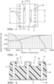
- FIG. 1 schematically shows an example embodiment of an antenna device 20.
- a substrate 22 includes a plurality of substrate integrated waveguides (SIWs).
- SIWs substrate integrated waveguides
- a first SIW 24 is established between conductive members 26, which are conductive vias in this example.
- a second SIW 34 is established between conductive members 36.
- Conductive members 38 establish a second input port 40 into the second SIW 34.
- a third SIW 44 defined between conductive members 46 is included in the illustrated example.
- Conductive members 48 establish a third input port 50 for the third SIW 44.
- all of the conductive members 36, 38, 46 and 48 are conductive vias.
- the portions of the substrate 22 within the SIWs 24, 34 and 44 are each referred to as a first portion of the substrate 22.
- the other portion of the substrate 22 outside of the SIWs is referred to as a second portion of the substrate 22.
- An exterior surface 51 of the substrate 22 includes a layer of electrically conductive material.
- the exterior surface 51 includes metal, such as copper.
- the exterior surfaces of the first portions of the substrate 22 include a plurality of first slots 52 and a plurality of second slots 54.
- the first slots 52 and the second slots 54 allow energy within the respective SIWs to radiate out through the slots 52 and 54.
- Each SIW with its slots 52 and 54 operates as an antenna.
- the first slots 52 emit radiation that has a different characteristic than the radiation emitted through the second slots 54.
- the characteristic that differs may be any of a power, phase or gain of the radiation.
- the different characteristic is a result of the different sizes of the first slots 52 compared to the second slots 54.
- Each of the second slots 54 is associated with one of the first slots 52.
- Figure 2 shows an example set of a first slot 52 and an associated second slot 54.
- the first slot 52 has a first length L 1 that is longer than a second length L 2 of the second slot 54. All first slots 52 are longer than their associated second slot 54 in the illustrated example.
- the different lengths L 1 and L 2 provide a radiation pattern that varies across a beam of radiation emitted by each SIW antenna.
- the different lengths result in different phases of the radiation and the arrangement of the first slots 52 along one side of the SIW and the second slots 54 along another side of the SIW provides a phase tilt that biases a gain of the radiation from the SIW antenna toward one side.
- Figure 3 includes a plot 60 of a gain of a radiation pattern across an example beam of radiation. At 62, the gain is higher than at 64 and is biased toward one side of the beam.
- a radiation pattern makes the example embodiment useful for middle range radar, for example, and provides a narrow elevation angle with a wide range azimuth angle over significant distances.
- Having the gain biased to one side like the example of Figure 3 allows for strategically placing a plurality of antenna devices 20 on a vehicle, for example, to achieve a desired sensing or detecting radiation pattern around the periphery of the vehicle.
- the associated first and second slots 52 and 54 are spaced apart by a spacing S.
- the spacing S varies along a length of the corresponding SIW.
- the spacing S is smaller near the input to the SIW and the ends of the SIW compared to the spacing between other associated first and second slots 52 and 54.
- the different spacings between the associated first slots 52 and second slots 54 accompanies a different distance between the respective slots 52 and 54 and the conductive members 26, 36, or 46 that establish the boundaries of the SIW. That distance shown at D in Figure 2 influences a strength of the radiation from the corresponding slots.
- a smaller distance D provides stronger radiation. Varying the spacing S and the distance D along a length of the SIWs achieves a desired tapering of the beam of radiation. In the illustrated example, the beam of radiation tapers off near the edges of the beam.
- the example embodiment of Figure 1 includes a plurality of parasitic interruptions 70 that minimize or eliminate interference or coupling between the SIW antennas.
- the parasitic interruptions 70 are also useful for reducing interference otherwise caused by other devices near the antenna device 20.
- the parasitic interruptions 70 include slots 72 in the exterior surface 51 of the second portion of the substrate outside of the SIWs.
- the slots 72 have a depth that corresponds to one-quarter of guided wavelength .
- the parasitic interruptions 70 also include a plurality of conductive connectors 74 on opposite sides of the slots 72.
- the slots 72 have a conductive coating or lining 80.
- the conductive lining 80 comprises a layer of metal, such as copper.
- the conductive connectors 74 establish a conductive connection between the exterior layer 51 and another conductive layer 82 that is near an opposite side of the substrate 22.
- the conductive layer 82 establishes or defines an exterior surface of the opposite side of the substrate 22 and operates as a ground layer.
- the conductive connectors 74 in this example are conductive vias.
- the conductive connectors 74 establish conductive fences that form or establish sides of a choke including the slot 72 between two rows of the conductive connectors 74. Some of the slots have the conductive connectors 74 on one side and the conductive members 26, 36 or 46 of one side of the adjacent SIW on the other side of the slot 72.
- the example shown in Figure 4 includes two of the slots 72 situated on the left (according to Figure 1 ) of the SIW 24 and the conductive members 26 also serve as conductive connectors to establish or define one side of one of the chokes shown in Figure 4 .
- Some of the example chokes of the parasitic interruptions 70 include the conductive members 28, 38, 48 that respectively establish the input ports 30, 40 and 50 as at least some of the conductive connectors on a side of one of the slots 72.
- the slots 72 and the conductive connectors 74 (and in some instances the conductive members 26, 28, 36, 38, 46, or 48) establish the chokes having generally U-shaped metal surface cross-sections between the SIW antennas that reduce antenna coupling.
- the chokes interrupt electrical energy or current flow along the exterior surface 51.
- the parasitic interruptions 70 ensure a desired profile or smoothness of the radiation pattern of the individual antennas of the antenna device 20.
- Figure 5 shows a desirable radiation pattern across three beams corresponding to an output beam of radiation from each of the SIW antennas. If the parasitic interruptions were not present, then there would be coupling between the SIW antennas and a resulting radiation pattern would be like that shown at 94 in Figure 6 . The coupling has the effect of causing dips, as shown at 96, in the radiation pattern, which is undesirable. The parasitic interruptions 70 guard against such dips. Additionally, the parasitic interruptions 70 allow for more antenna devices 20 to be situated near each other to provide wide radiation beam coverage from each antenna, which allows for more comprehensive and consistent scanning or detecting around the periphery or exterior of a vehicle.
Landscapes
- Engineering & Computer Science (AREA)
- Manufacturing & Machinery (AREA)
- Variable-Direction Aerials And Aerial Arrays (AREA)
- Waveguide Aerials (AREA)
- Details Of Aerials (AREA)
Abstract
Description
- Increasing amounts of technology are included on automotive vehicles. Radar and lidar sensing devices provide the capability to detect objects in a vicinity or pathway of the vehicle. Many such devices include a radiating antenna that emits the radiation used for object detection.
- While different antenna types have proven useful, they are not without shortcomings or drawbacks. For example, some antennas that are useful for short or medium range detection have the capability of covering a wide field of view, but experience high loss when the electromagnetic wave radiated from the antenna passes through the fascia of the vehicle. Such high losses are typically associated with vertical polarization of the antenna. One attempt to address that problem is to incorporate horizontal polarization. The difficulty associated with horizontal polarization, however, is that the impedance bandwidth is typically too narrow to satisfy production requirements. One approach to increase the impedance bandwidth includes increasing the thickness of the antenna substrate material. A disadvantage associated with that approach is that it increases cost.
- Another difficulty associated with some known radar antenna configurations is the occurrence of high frequency ripples resulting from radiation scattering from nearby antennas, electronic components on the vehicle, and other metal or dielectric materials in close proximity to the antennas. A further complication is that the ripples in the radiation pattern for each antenna occur at different angles and that affects the uniformity of the radiation patterns of all the antennas used for radar. A non-uniform radiation pattern significantly lowers the angle finding accuracy of the radar system.
- An illustrative example antenna device includes a substrate. A plurality of conductive members in the substrate establish a substrate integrated waveguide (SIW). A first portion of the substrate is within the SIW and a second portion of the substrate is outside the SIW. A plurality of first slots are on an exterior surface of the first portion of the substrate. A plurality of second slots are also on the exterior surface of the first portion of the substrate. Each of the second slots is associated with a respective one of the first slots. The first and second slots are configured to establish a radiation pattern that varies across a beam of radiation emitted by the antenna device. A plurality of parasitic interruptions include at least a first one of the parasitic interruptions on a first side of the SIW and at least a second one of the parasitic interruptions on a second, opposite side of the SIW.
- In an example embodiment having one or more features of the antenna device of the previous paragraph, the parasitic interruptions respectively include a slot along an exterior surface of the second portion of the substrate, and at least one conductive connector establishing a conductive connection between the exterior surface of the second portion near two sides of the slot and a conductive layer near an opposite side of the substrate.
- In an example embodiment having one or more features of the antenna device of any of the previous paragraphs, the at least one conductive connector comprises a plurality of conductive members.
- In an example embodiment having one or more features of the antenna device of any of the previous paragraphs, the parasitic interruption slots have a depth corresponding to one-quarter of a guided wavelength.
- In an example embodiment having one or more features of the antenna device of any of the previous paragraphs, the parasitic interruption slots are lined with a conductive material.
- In an example embodiment having one or more features of the antenna device of any of the previous paragraphs, the conductive material comprises metal and the conductive layer near the opposite side of the substrate comprises metal.
- In an example embodiment having one or more features of the antenna device of any of the previous paragraphs, the metal is copper.
- In an example embodiment having one or more features of the antenna device of any of the previous paragraphs, the first slots emit radiation having a first characteristic and the second slots emit radiation having a second characteristic that is different than the first characteristic.
- In an example embodiment having one or more features of the antenna device of any of the previous paragraphs, the first and second characteristics respectively comprise at least one of a power of emitted radiation, a phase of emitted radiation, or a gain of emitted radiation.
- In an example embodiment having one or more features of the antenna device of any of the previous paragraphs, the first characteristic and the second characteristic bias a gain of the beam of radiation toward one side of the radiation pattern.
- In an example embodiment having one or more features of the antenna device of any of the previous paragraphs, the first slots have a first length, the second slots have a second length, and the first and second characteristics are based on the first and second lengths, respectively.
- In an example embodiment having one or more features of the antenna device of any of the previous paragraphs, a spacing between associated first and second slots varies along a length of the SIW.
- In an example embodiment having one or more features of the antenna device of any of the previous paragraphs, the spacing controls a strength of radiation emitted through the associated first and second slots.
- In an example embodiment having one or more features of the antenna device of any of the previous paragraphs, the substrate includes a plurality of SIWs, at least a first one of the parasitic interruptions is on a first side of each SIW, and at least a second one of the parasitic interruptions is on a second, opposite side of each SIW.
- In an example embodiment having one or more features of the antenna device of any of the previous paragraphs, each SIW includes an input port between opposite ends of the SIW, at least some of the parasitic interruptions are on one side of a respective one of the input ports, and at least some others of the parasitic interruptions are on a different side of the respective one of the input ports.
- In an example embodiment having one or more features of the antenna device of any of the previous paragraphs, the SIWs are aligned parallel to each other, the parasitic interruptions are parallel to the SIWs, an input port to at least one of the SIWs is situated between adjacent SIWs; and at least some of the parasitic interruptions are situated between adjacent SIWs.
- In an example embodiment having one or more features of the antenna device of any of the previous paragraphs, a number of the parasitic interruptions on the first side of the SIW differs from a number of the parasitic interruptions on the second side of the SIW.
- In an example embodiment having one or more features of the antenna device of any of the previous paragraphs, the exterior surface comprises a layer of metal.
- An illustrative example of a method of making an antenna device includes: establishing a plurality of first slots on an exterior surface of a first portion of a substrate, the substrate including a substrate integrated waveguide (SIW), the first portion of the substrate being within the SIW and a second portion of the substrate being outside the SIW; establishing a plurality of second slots on the exterior surface of the first portion of the substrate, each of the second slots being associated with a respective one of the first slots, the first and second slots being configured to establish a radiation pattern that varies across a beam of radiation emitted by the antenna device; and establishing a plurality of parasitic interruptions, at least a first one of the parasitic interruptions being on a first side of the SIW and at least a second one of the parasitic interruptions being on a second, opposite side of the SIW.
- In an example embodiment having one or more features of the method of the previous paragraph, the exterior surface comprises a first conductive layer. Establishing the parasitic interruptions, respectively, includes forming a slot along an exterior surface of the second portion of the substrate, lining the formed slot with a conductive material, and establishing a conductive connection between the exterior surface of the second portion near two sides of the slot and a conductive layer near an opposite side of the substrate.
- Various features and advantages of at least one disclosed example embodiment will become apparent to those skilled in the art from the following detailed description. The drawings that accompany the detailed description can be briefly describe as follows.
-
-
Figure 1 schematically illustrates an example embodiment of an antenna device. -
Figure 2 illustrates selected features of the embodiment ofFigure 1 . -
Figure 3 graphically illustrates an example radiation pattern emitted by an example embodiment of an antenna device. -
Figure 4 is a cross-sectional illustration taken along the lines 4-4 inFigure 1 . -
Figure 5 graphically illustrates an example radiation pattern emitted by the embodiment ofFigure 1 . -
Figure 6 graphically illustrates an example radiation pattern that may result if features of the embodiment ofFigure 1 were not present. -
Figure 1 schematically shows an example embodiment of anantenna device 20. Asubstrate 22 includes a plurality of substrate integrated waveguides (SIWs). Afirst SIW 24 is established betweenconductive members 26, which are conductive vias in this example.Conductive members 28, which are also conductive vias in this example, establish afirst input port 30 of thefirst SIW 24. Asecond SIW 34 is established betweenconductive members 36. Conductive members 38 establish asecond input port 40 into thesecond SIW 34. Athird SIW 44 defined betweenconductive members 46 is included in the illustrated example.Conductive members 48 establish athird input port 50 for thethird SIW 44. In this example, all of theconductive members - The portions of the
substrate 22 within theSIWs substrate 22. The other portion of thesubstrate 22 outside of the SIWs is referred to as a second portion of thesubstrate 22. - An
exterior surface 51 of thesubstrate 22 includes a layer of electrically conductive material. In this example, theexterior surface 51 includes metal, such as copper. The exterior surfaces of the first portions of thesubstrate 22 include a plurality offirst slots 52 and a plurality ofsecond slots 54. Thefirst slots 52 and thesecond slots 54 allow energy within the respective SIWs to radiate out through theslots slots - The
first slots 52 emit radiation that has a different characteristic than the radiation emitted through thesecond slots 54. The characteristic that differs may be any of a power, phase or gain of the radiation. In the illustrated example, the different characteristic is a result of the different sizes of thefirst slots 52 compared to thesecond slots 54. - Each of the
second slots 54 is associated with one of thefirst slots 52.Figure 2 shows an example set of afirst slot 52 and an associatedsecond slot 54. Thefirst slot 52 has a first length L1 that is longer than a second length L2 of thesecond slot 54. Allfirst slots 52 are longer than their associatedsecond slot 54 in the illustrated example. The different lengths L1 and L2 provide a radiation pattern that varies across a beam of radiation emitted by each SIW antenna. The different lengths result in different phases of the radiation and the arrangement of thefirst slots 52 along one side of the SIW and thesecond slots 54 along another side of the SIW provides a phase tilt that biases a gain of the radiation from the SIW antenna toward one side. -
Figure 3 includes a plot 60 of a gain of a radiation pattern across an example beam of radiation. At 62, the gain is higher than at 64 and is biased toward one side of the beam. Such a radiation pattern makes the example embodiment useful for middle range radar, for example, and provides a narrow elevation angle with a wide range azimuth angle over significant distances. Having the gain biased to one side like the example ofFigure 3 allows for strategically placing a plurality ofantenna devices 20 on a vehicle, for example, to achieve a desired sensing or detecting radiation pattern around the periphery of the vehicle. - The associated first and
second slots second slots first slots 52 andsecond slots 54 accompanies a different distance between therespective slots conductive members Figure 2 influences a strength of the radiation from the corresponding slots. A smaller distance D provides stronger radiation. Varying the spacing S and the distance D along a length of the SIWs achieves a desired tapering of the beam of radiation. In the illustrated example, the beam of radiation tapers off near the edges of the beam. - The example embodiment of
Figure 1 includes a plurality ofparasitic interruptions 70 that minimize or eliminate interference or coupling between the SIW antennas. Theparasitic interruptions 70 are also useful for reducing interference otherwise caused by other devices near theantenna device 20. Theparasitic interruptions 70 includeslots 72 in theexterior surface 51 of the second portion of the substrate outside of the SIWs. Theslots 72 have a depth that corresponds to one-quarter of guided wavelength . Theparasitic interruptions 70 also include a plurality ofconductive connectors 74 on opposite sides of theslots 72. - As shown in
Figure 4 , theslots 72 have a conductive coating or lining 80. In this example, theconductive lining 80 comprises a layer of metal, such as copper. Theconductive connectors 74 establish a conductive connection between theexterior layer 51 and anotherconductive layer 82 that is near an opposite side of thesubstrate 22. In this example, theconductive layer 82 establishes or defines an exterior surface of the opposite side of thesubstrate 22 and operates as a ground layer. - The
conductive connectors 74 in this example are conductive vias. Theconductive connectors 74 establish conductive fences that form or establish sides of a choke including theslot 72 between two rows of theconductive connectors 74. Some of the slots have theconductive connectors 74 on one side and theconductive members slot 72. The example shown inFigure 4 includes two of theslots 72 situated on the left (according toFigure 1 ) of theSIW 24 and theconductive members 26 also serve as conductive connectors to establish or define one side of one of the chokes shown inFigure 4 . Some of the example chokes of theparasitic interruptions 70 include theconductive members input ports slots 72. Theslots 72 and the conductive connectors 74 (and in some instances theconductive members exterior surface 51. - As shown in
Figure 1 there are different numbers ofparasitic interruptions 70 on two sides of the SIWs based on the number ofslots 72 on each side. Given the biased gain of the example SIW antennas, the different numbers of slots are situated to address the way in which energy may otherwise travel along theexterior surface 51 and result in coupling between the SIW antennas. - The
parasitic interruptions 70 ensure a desired profile or smoothness of the radiation pattern of the individual antennas of theantenna device 20.Figure 5 shows a desirable radiation pattern across three beams corresponding to an output beam of radiation from each of the SIW antennas. If the parasitic interruptions were not present, then there would be coupling between the SIW antennas and a resulting radiation pattern would be like that shown at 94 inFigure 6 . The coupling has the effect of causing dips, as shown at 96, in the radiation pattern, which is undesirable. Theparasitic interruptions 70 guard against such dips. Additionally, theparasitic interruptions 70 allow formore antenna devices 20 to be situated near each other to provide wide radiation beam coverage from each antenna, which allows for more comprehensive and consistent scanning or detecting around the periphery or exterior of a vehicle. - The preceding description is illustrative rather than limiting in nature. Variations and modifications to the disclosed example embodiments may become apparent to those skilled in the art without departing from the essence of this invention. The scope of legal protection provided to this invention can only be determined by studying the following claims.
Claims (14)
- An antenna device (20), comprising:a substrate (22);a plurality of conductive members (26, 36, 46) in the substrate (22), the conductive members (26, 36, 46) establishing a substrate integrated waveguide (24, 34, 44), SIW, a first portion of the substrate (22) being within the SIW (24, 34, 44) and a second portion of the substrate (22) being outside the SIW (24, 34, 44);a plurality of first slots (52) on an exterior surface (51) of the first portion of the substrate (22);a plurality of second slots (54) on the exterior surface (51) of the first portion of the substrate (22), each of the second slots (54) being associated with a respective one of the first slots (52), the first and second slots (52, 54) being configured to establish a radiation pattern that varies across a beam of radiation emitted by the antenna device (20); and
a plurality of parasitic interruptions (70), at least a first one of the parasitic interruptions (70) being on a first side of the SIW (24, 34, 44) and at least a second one of the parasitic interruptions (70) being on a second, opposite side of the SIW (24, 34, 44), the first one of the parasitic interruptions having a first set of slots (72) and the second one of the parasitic interruptions having a second set of slots (72), with at least one of:
a number of slots (72) in the first set differs from a number of slots (72) in the second set; orthe slots of the first set have a different length than the slots of the second set. - The antenna device of claim 1, wherein each of the plurality of the first slots (52) on the exterior surface (51) of the first portion of the substrate (22) include spacings from the plurality of conductive members (26, 36, 46) of the substrate (22), the spacings varying along the SIW (24, 34, 44) and effective to enable stronger radiation from smaller of the spacings relative to weaker radiation from larger of the spacings.
- The antenna device of claim 2, wherein the varying of the spacings is effective to achieve a tapering of the beam of radiation emitted by the antenna device (20).
- The antenna device of any one of the preceding claims, wherein the parasitic interruptions respectively comprise:
at least one conductive connector (74) establishing a conductive connection between an exterior surface (51) of the second portion near two sides of the first set of one or more slots (72) and a conductive layer (82) near an opposite side of the substrate (22). - The antenna device (20) of any of the preceding claims, whereinthe first slots (52) emit radiation having a first characteristic; andthe second slots (54) emit radiation having a second characteristic that is different than the first characteristic, the first characteristic and the second characteristic biasing a gain of the beam of radiation toward one side of the radiation pattern.
- The antenna device (20) of claim 5, whereinthe first slots (52) have a first length;the second slots (54) have a second length; andthe first and second characteristics are based on the first and second lengths, respectively.
- The antenna device (20) of any of the preceding claims, wherein
the substrate (22) includes a plurality of SIWs (24, 34, 44). - The antenna device (20) of claim 7, whereineach SIW (24, 34, 44) includes an input port (30, 40, 50) between opposite ends of the SIW (24, 34, 44);at least some of the parasitic interruptions (70) are on one side of a respective one of the input ports (30, 40, 50); andat least some others of the parasitic interruptions (70) are on a different side of the respective one of the input ports (30, 40, 50).
- The antenna device (20) of claim 7, whereinthe SIWs (24, 34, 44) are aligned parallel to each other;the parasitic interruptions (70) are parallel to the SIWs (24, 34, 44);an input port (30, 40, 50) to at least one of the SIWs (24, 34, 44) is situated between adjacent SIWs (24, 34, 44); andat least some of the parasitic interruptions (70) are situated between adjacent SIWs (24, 34, 44).
- The antenna device (20) of claim 1, wherein each of the plurality of the first slots (52) on the exterior surface (51) of the first portion of the substrate (22) are longer than each of the plurality of the second slots (54) on the exterior surface (51) of the first portion.
- The antenna device (20) of claim 1, wherein each of the plurality of the first slots (52) on the exterior surface (51) of the first portion of the substrate (22) has an associated one of the plurality of the second slots (54) on the exterior surface (51) of the first portion, each of the first slots (52) and the second slots (54) having a spacing between each of the respective associated slots, the spacing varying between at least two of each of the spacings between the respective slots;
wherein the spacings are optionally smaller at ends of the waveguide (24, 34, 44). - The antenna device (20) of claim 1, wherein the first set of one or more slots (72) and the second set of one or more slots (72) have a depth corresponding to one-quarter of a guided wavelength.
- The antenna device (20) of claim 1, wherein the number of slots (72) in the first set differs from the number of slots (72) in the second set.
- The antenna device of claim 1, wherein the slots of the first set have a different length than the slots of the second set.
Applications Claiming Priority (2)
| Application Number | Priority Date | Filing Date | Title |
|---|---|---|---|
| US16/294,528 US10944184B2 (en) | 2019-03-06 | 2019-03-06 | Slot array antenna including parasitic features |
| EP20155296.5A EP3706242B1 (en) | 2019-03-06 | 2020-02-04 | Slot array antenna including parasitic features |
Related Parent Applications (1)
| Application Number | Title | Priority Date | Filing Date |
|---|---|---|---|
| EP20155296.5A Division EP3706242B1 (en) | 2019-03-06 | 2020-02-04 | Slot array antenna including parasitic features |
Publications (2)
| Publication Number | Publication Date |
|---|---|
| EP4369523A2 true EP4369523A2 (en) | 2024-05-15 |
| EP4369523A3 EP4369523A3 (en) | 2024-07-24 |
Family
ID=69468385
Family Applications (2)
| Application Number | Title | Priority Date | Filing Date |
|---|---|---|---|
| EP20155296.5A Active EP3706242B1 (en) | 2019-03-06 | 2020-02-04 | Slot array antenna including parasitic features |
| EP24167446.4A Pending EP4369523A3 (en) | 2019-03-06 | 2020-02-04 | Slot array antenna including parasitic features |
Family Applications Before (1)
| Application Number | Title | Priority Date | Filing Date |
|---|---|---|---|
| EP20155296.5A Active EP3706242B1 (en) | 2019-03-06 | 2020-02-04 | Slot array antenna including parasitic features |
Country Status (3)
| Country | Link |
|---|---|
| US (2) | US10944184B2 (en) |
| EP (2) | EP3706242B1 (en) |
| CN (2) | CN111668598B (en) |
Families Citing this family (32)
| Publication number | Priority date | Publication date | Assignee | Title |
|---|---|---|---|---|
| US10944184B2 (en) * | 2019-03-06 | 2021-03-09 | Aptiv Technologies Limited | Slot array antenna including parasitic features |
| US11165149B2 (en) * | 2020-01-30 | 2021-11-02 | Aptiv Technologies Limited | Electromagnetic band gap structure (EBG) |
| US11757166B2 (en) | 2020-11-10 | 2023-09-12 | Aptiv Technologies Limited | Surface-mount waveguide for vertical transitions of a printed circuit board |
| CN112688081B (en) * | 2020-12-15 | 2022-05-10 | 重庆邮电大学 | A broadband cavity-backed planar slot array antenna based on dielectric integrated waveguide |
| JP7726219B2 (en) * | 2020-12-17 | 2025-08-20 | ソニーグループ株式会社 | Antenna device, terminator and terminal device |
| US11901601B2 (en) | 2020-12-18 | 2024-02-13 | Aptiv Technologies Limited | Waveguide with a zigzag for suppressing grating lobes |
| US11749883B2 (en) | 2020-12-18 | 2023-09-05 | Aptiv Technologies Limited | Waveguide with radiation slots and parasitic elements for asymmetrical coverage |
| US11681015B2 (en) | 2020-12-18 | 2023-06-20 | Aptiv Technologies Limited | Waveguide with squint alteration |
| US11668787B2 (en) * | 2021-01-29 | 2023-06-06 | Aptiv Technologies Limited | Waveguide with lobe suppression |
| US12058804B2 (en) | 2021-02-09 | 2024-08-06 | Aptiv Technologies AG | Formed waveguide antennas of a radar assembly |
| US11721905B2 (en) | 2021-03-16 | 2023-08-08 | Aptiv Technologies Limited | Waveguide with a beam-forming feature with radiation slots |
| US11855346B2 (en) * | 2021-03-19 | 2023-12-26 | Veoneer Us, Llc | Parallel plate slot array antenna with defined beam squint |
| US11616306B2 (en) | 2021-03-22 | 2023-03-28 | Aptiv Technologies Limited | Apparatus, method and system comprising an air waveguide antenna having a single layer material with air channels therein which is interfaced with a circuit board |
| EP4084222A1 (en) * | 2021-04-30 | 2022-11-02 | Aptiv Technologies Limited | Dielectric loaded waveguide for low loss signal distributions and small form factor antennas |
| US11962085B2 (en) | 2021-05-13 | 2024-04-16 | Aptiv Technologies AG | Two-part folded waveguide having a sinusoidal shape channel including horn shape radiating slots formed therein which are spaced apart by one-half wavelength |
| US11749884B2 (en) | 2021-05-17 | 2023-09-05 | HJWAVE Co., Ltd. | Multi-layer antenna structure supporting wide band and wide angle |
| KR102464792B1 (en) * | 2021-05-17 | 2022-11-09 | 주식회사 에이치제이웨이브 | Multi Layer Antenna Structure with Wideband Wide Angle |
| KR20240008852A (en) * | 2021-05-19 | 2024-01-19 | 후버 앤드 주흐너 아게 | Antenna devices for automotive radar applications |
| US11668788B2 (en) * | 2021-07-08 | 2023-06-06 | Veoneer Us, Llc | Phase-compensated waveguides and related sensor assemblies |
| US11616282B2 (en) | 2021-08-03 | 2023-03-28 | Aptiv Technologies Limited | Transition between a single-ended port and differential ports having stubs that match with input impedances of the single-ended and differential ports |
| US12224502B2 (en) | 2021-10-14 | 2025-02-11 | Aptiv Technologies AG | Antenna-to-printed circuit board transition |
| CN114065559B (en) * | 2022-01-18 | 2022-04-15 | 常州星宇车灯股份有限公司 | Design method of substrate integrated waveguide antenna |
| US12456816B2 (en) | 2022-05-02 | 2025-10-28 | Aptiv Technologies AG | Waveguide with slot antennas and reflectors |
| US12265172B2 (en) | 2022-05-25 | 2025-04-01 | Aptiv Technologies AG | Vertical microstrip-to-waveguide transition |
| US12424767B2 (en) | 2022-11-15 | 2025-09-23 | Aptiv Technologies AG | Planar surface features for waveguide and antenna |
| US12537308B2 (en) | 2023-01-24 | 2026-01-27 | Aptiv Technologies AG | Symmetrical two-piece waveguide |
| US12148992B2 (en) | 2023-01-25 | 2024-11-19 | Aptiv Technologies AG | Hybrid horn waveguide antenna |
| KR102876493B1 (en) * | 2023-02-16 | 2025-10-27 | 주식회사 에이치엘클레무브 | Double slot array antenna design method and double slot array antenna designed thereby |
| US12506272B2 (en) | 2023-05-16 | 2025-12-23 | Aptiv Technologies AG | Production-tolerant multi-part antenna system |
| US12627020B2 (en) | 2023-05-18 | 2026-05-12 | Aptiv Technologies AG | Waveguide with a curved-wall low-pass filter |
| US20250110202A1 (en) * | 2023-10-02 | 2025-04-03 | Magna Electronics, Llc | Automotive sensor module with backscattering cancellation |
| DE102024202153A1 (en) * | 2024-03-07 | 2025-09-11 | Robert Bosch Gesellschaft mit beschränkter Haftung | Antenna device and method for producing an antenna device |
Family Cites Families (35)
| Publication number | Priority date | Publication date | Assignee | Title |
|---|---|---|---|---|
| US4291312A (en) * | 1977-09-28 | 1981-09-22 | The United States Of America As Represented By The Secretary Of The Navy | Dual ground plane coplanar fed microstrip antennas |
| US5047738A (en) * | 1990-10-09 | 1991-09-10 | Hughes Aircraft Company | Ridged waveguide hybrid |
| US7460084B2 (en) * | 2005-10-19 | 2008-12-02 | Northrop Grumman Corporation | Radio frequency holographic transformer |
| GB0706296D0 (en) * | 2007-03-30 | 2007-05-09 | Nortel Networks Ltd | Low cost lightweight antenna technology |
| US8669834B2 (en) * | 2008-03-18 | 2014-03-11 | Shi Cheng | Substrate integrated waveguide |
| IT1398678B1 (en) | 2009-06-11 | 2013-03-08 | Mbda italia spa | SLOT SLIP ANTENNA WITH POWER SUPPLY IN WAVE GUIDE AND PROCEDURE FOR REALIZING THE SAME |
| US8576023B1 (en) * | 2010-04-20 | 2013-11-05 | Rockwell Collins, Inc. | Stripline-to-waveguide transition including metamaterial layers and an aperture ground plane |
| JP5253468B2 (en) | 2010-09-03 | 2013-07-31 | 株式会社東芝 | Antenna device and radar device |
| KR101092846B1 (en) | 2010-09-30 | 2011-12-14 | 서울대학교산학협력단 | Serial slot array antenna |
| RU2590937C2 (en) * | 2010-10-15 | 2016-07-10 | Де Инвеншн Сайенс Фанд Уан, ЭлЭлСи | Surface scattering antennae |
| US8648676B2 (en) * | 2011-05-06 | 2014-02-11 | The Royal Institution For The Advancement Of Learning/Mcgill University | Tunable substrate integrated waveguide components |
| US8670638B2 (en) * | 2011-09-29 | 2014-03-11 | Broadcom Corporation | Signal distribution and radiation in a wireless enabled integrated circuit (IC) using a leaky waveguide |
| US20130300602A1 (en) * | 2012-05-08 | 2013-11-14 | Samsung Electronics Co., Ltd. | Antenna arrays with configurable polarizations and devices including such antenna arrays |
| US9685708B2 (en) * | 2012-08-23 | 2017-06-20 | Ntn Corporation | Waveguide tube slot antenna and wireless device provided therewith |
| WO2014154231A1 (en) * | 2013-03-24 | 2014-10-02 | Telefonaktiebolaget L M Ericsson (Publ) | A siw antenna arrangement |
| US9882288B2 (en) * | 2014-05-02 | 2018-01-30 | The Invention Science Fund I Llc | Slotted surface scattering antennas |
| US9851436B2 (en) | 2015-01-05 | 2017-12-26 | Delphi Technologies, Inc. | Radar antenna assembly with panoramic detection |
| US9985331B2 (en) * | 2015-07-07 | 2018-05-29 | Huawei Technologies Co., Ltd. | Substrate integrated waveguide switch |
| IL241951B (en) * | 2015-10-07 | 2018-04-30 | Israel Aerospace Ind Ltd | Waveguide elements, fabrication techniques and arrangements thereof |
| WO2017137224A1 (en) * | 2016-02-12 | 2017-08-17 | Telefonaktiebolaget Lm Ericsson (Publ) | A transition arrangement comprising a contactless transition or connection between an siw and a waveguide or an antenna |
| US10468738B2 (en) * | 2016-03-15 | 2019-11-05 | Aptiv Technologies Limited | Signaling device including a substrate integrated waveguide coupled to a signal generator through a ball grid array |
| JP6686820B2 (en) * | 2016-03-17 | 2020-04-22 | 住友電気工業株式会社 | Antenna and radar |
| TWM528022U (en) * | 2016-03-31 | 2016-09-01 | 道安達股份有限公司 | Dual slot siw antenna unit and array module thereof |
| TWI610492B (en) | 2016-03-31 | 2018-01-01 | 為昇科科技股份有限公司 | Dual slot siw antenna unit and array module thereof |
| US10613216B2 (en) * | 2016-05-31 | 2020-04-07 | Honeywell International Inc. | Integrated digital active phased array antenna and wingtip collision avoidance system |
| US11605903B2 (en) * | 2016-08-10 | 2023-03-14 | Mitsubishi Electric Corporation | Array antenna apparatus and method for manufacturing array antenna apparatus |
| US20180123245A1 (en) * | 2016-10-28 | 2018-05-03 | Broadcom Corporation | Broadband antenna array for wireless communications |
| JP2018182743A (en) * | 2017-04-18 | 2018-11-15 | 日本電産株式会社 | Slot array antenna |
| RU2652169C1 (en) * | 2017-05-25 | 2018-04-25 | Самсунг Электроникс Ко., Лтд. | Antenna unit for a telecommunication device and a telecommunication device |
| US10186787B1 (en) * | 2017-09-05 | 2019-01-22 | Honeywell International Inc. | Slot radar antenna with gas-filled waveguide and PCB radiating slots |
| DE102018124924A1 (en) * | 2017-10-10 | 2019-04-11 | Nidec Corporation | Waveguiding device |
| CN111344895A (en) * | 2017-10-13 | 2020-06-26 | 康普技术有限责任公司 | Power couplers and related equipment with antenna element power absorbers |
| US10879616B2 (en) * | 2018-08-30 | 2020-12-29 | University Of Electronic Science And Technology Of China | Shared-aperture antenna |
| US10944184B2 (en) * | 2019-03-06 | 2021-03-09 | Aptiv Technologies Limited | Slot array antenna including parasitic features |
| US11165149B2 (en) * | 2020-01-30 | 2021-11-02 | Aptiv Technologies Limited | Electromagnetic band gap structure (EBG) |
-
2019
- 2019-03-06 US US16/294,528 patent/US10944184B2/en active Active
-
2020
- 2020-02-04 EP EP20155296.5A patent/EP3706242B1/en active Active
- 2020-02-04 EP EP24167446.4A patent/EP4369523A3/en active Pending
- 2020-03-05 CN CN202010146513.9A patent/CN111668598B/en active Active
- 2020-03-05 CN CN202210993090.3A patent/CN115579624B/en active Active
-
2021
- 2021-03-09 US US17/196,777 patent/US11374333B2/en active Active
Also Published As
| Publication number | Publication date |
|---|---|
| CN111668598B (en) | 2022-08-09 |
| EP3706242B1 (en) | 2024-04-03 |
| CN111668598A (en) | 2020-09-15 |
| CN115579624A (en) | 2023-01-06 |
| EP3706242A1 (en) | 2020-09-09 |
| US10944184B2 (en) | 2021-03-09 |
| US11374333B2 (en) | 2022-06-28 |
| US20200287293A1 (en) | 2020-09-10 |
| US20210218154A1 (en) | 2021-07-15 |
| CN115579624B (en) | 2025-10-28 |
| EP4369523A3 (en) | 2024-07-24 |
Similar Documents
| Publication | Publication Date | Title |
|---|---|---|
| US11374333B2 (en) | Slot array antenna including parasitic features | |
| EP3522297B1 (en) | Wide angle coverage antenna | |
| US10431895B2 (en) | Dual slot SIW antenna unit and array module thereof | |
| KR102033311B1 (en) | Microstripline-fed slot array antenna and manufacturing method thereof | |
| WO2014142202A1 (en) | Antenna device having patch antenna | |
| EP2211423A2 (en) | Radar antenna | |
| Joseph et al. | Series-fed millimeter-wave antenna array based on microstrip line structure | |
| US11411319B2 (en) | Antenna apparatus | |
| EP2816666A1 (en) | Wide-angle antenna and array antenna | |
| KR102224626B1 (en) | Waveguide slot array antenna | |
| US20170365935A1 (en) | Array antenna | |
| US20080266195A1 (en) | Waveguide Slot Array Antenna Assembly | |
| Jia et al. | A 24 GHz microstrip antenna array with large space and narrow beamwidth | |
| TWM531066U (en) | Antenna unit with wide beam | |
| EP3846285B1 (en) | Antenna for improving influence of surface waves and increasing beamwidth | |
| CN109428175A (en) | Antenna element, trailer-mounted radar and automobile | |
| KR101679553B1 (en) | Traveling-wave antenna with improved beam tilt deviation | |
| KR102120455B1 (en) | Automotive Radar Antenna with Wide Angle Characteristics | |
| JP2022113142A (en) | High-gain tightly coupled dipole antenna array | |
| CN109428176A (en) | Antenna element, trailer-mounted radar and automobile | |
| CN109428165A (en) | Antenna element, trailer-mounted radar and automobile | |
| CN110120582B (en) | Antenna device | |
| KR101775516B1 (en) | Crpa array antenna | |
| JP2023503294A (en) | Electromagnetic bandgap structure | |
| US20170040709A1 (en) | Radar apparatus |
Legal Events
| Date | Code | Title | Description |
|---|---|---|---|
| PUAI | Public reference made under article 153(3) epc to a published international application that has entered the european phase |
Free format text: ORIGINAL CODE: 0009012 |
|
| STAA | Information on the status of an ep patent application or granted ep patent |
Free format text: STATUS: THE APPLICATION HAS BEEN PUBLISHED |
|
| AC | Divisional application: reference to earlier application |
Ref document number: 3706242 Country of ref document: EP Kind code of ref document: P |
|
| AK | Designated contracting states |
Kind code of ref document: A2 Designated state(s): AL AT BE BG CH CY CZ DE DK EE ES FI FR GB GR HR HU IE IS IT LI LT LU LV MC MK MT NL NO PL PT RO RS SE SI SK SM TR |
|
| PUAL | Search report despatched |
Free format text: ORIGINAL CODE: 0009013 |
|
| REG | Reference to a national code |
Ref country code: DE Ref legal event code: R079 Free format text: PREVIOUS MAIN CLASS: H01Q0021000000 Ipc: H01Q0001520000 |
|
| AK | Designated contracting states |
Kind code of ref document: A3 Designated state(s): AL AT BE BG CH CY CZ DE DK EE ES FI FR GB GR HR HU IE IS IT LI LT LU LV MC MK MT NL NO PL PT RO RS SE SI SK SM TR |
|
| RIC1 | Information provided on ipc code assigned before grant |
Ipc: H01Q 21/00 20060101ALI20240620BHEP Ipc: H01Q 13/22 20060101ALI20240620BHEP Ipc: H01Q 1/52 20060101AFI20240620BHEP |
|
| STAA | Information on the status of an ep patent application or granted ep patent |
Free format text: STATUS: REQUEST FOR EXAMINATION WAS MADE |
|
| 17P | Request for examination filed |
Effective date: 20240913 |
|
| RBV | Designated contracting states (corrected) |
Designated state(s): AL AT BE BG CH CY CZ DE DK EE ES FI FR GB GR HR HU IE IS IT LI LT LU LV MC MK MT NL NO PL PT RO RS SE SI SK SM TR |
|
| RAP1 | Party data changed (applicant data changed or rights of an application transferred) |
Owner name: APTIV TECHNOLOGIES AG |
|
| STAA | Information on the status of an ep patent application or granted ep patent |
Free format text: STATUS: EXAMINATION IS IN PROGRESS |
|
| 17Q | First examination report despatched |
Effective date: 20260223 |