EP4369408A1 - Transistor with metal field plate contact - Google Patents
Transistor with metal field plate contact Download PDFInfo
- Publication number
- EP4369408A1 EP4369408A1 EP23198686.0A EP23198686A EP4369408A1 EP 4369408 A1 EP4369408 A1 EP 4369408A1 EP 23198686 A EP23198686 A EP 23198686A EP 4369408 A1 EP4369408 A1 EP 4369408A1
- Authority
- EP
- European Patent Office
- Prior art keywords
- trench isolation
- shallow trench
- gate
- isolation structure
- contact
- Prior art date
- Legal status (The legal status is an assumption and is not a legal conclusion. Google has not performed a legal analysis and makes no representation as to the accuracy of the status listed.)
- Pending
Links
Images


Classifications
-
- H—ELECTRICITY
- H10—SEMICONDUCTOR DEVICES; ELECTRIC SOLID-STATE DEVICES NOT OTHERWISE PROVIDED FOR
- H10D—INORGANIC ELECTRIC SEMICONDUCTOR DEVICES
- H10D30/00—Field-effect transistors [FET]
- H10D30/60—Insulated-gate field-effect transistors [IGFET]
- H10D30/64—Double-diffused metal-oxide semiconductor [DMOS] FETs
- H10D30/65—Lateral DMOS [LDMOS] FETs
- H10D30/655—Lateral DMOS [LDMOS] FETs having edge termination structures
-
- H—ELECTRICITY
- H10—SEMICONDUCTOR DEVICES; ELECTRIC SOLID-STATE DEVICES NOT OTHERWISE PROVIDED FOR
- H10D—INORGANIC ELECTRIC SEMICONDUCTOR DEVICES
- H10D30/00—Field-effect transistors [FET]
- H10D30/60—Insulated-gate field-effect transistors [IGFET]
- H10D30/64—Double-diffused metal-oxide semiconductor [DMOS] FETs
- H10D30/65—Lateral DMOS [LDMOS] FETs
-
- H—ELECTRICITY
- H10—SEMICONDUCTOR DEVICES; ELECTRIC SOLID-STATE DEVICES NOT OTHERWISE PROVIDED FOR
- H10D—INORGANIC ELECTRIC SEMICONDUCTOR DEVICES
- H10D30/00—Field-effect transistors [FET]
- H10D30/01—Manufacture or treatment
- H10D30/021—Manufacture or treatment of FETs having insulated gates [IGFET]
- H10D30/0221—Manufacture or treatment of FETs having insulated gates [IGFET] having asymmetry in the channel direction, e.g. lateral high-voltage MISFETs having drain offset region or extended-drain MOSFETs [EDMOS]
-
- H—ELECTRICITY
- H10—SEMICONDUCTOR DEVICES; ELECTRIC SOLID-STATE DEVICES NOT OTHERWISE PROVIDED FOR
- H10D—INORGANIC ELECTRIC SEMICONDUCTOR DEVICES
- H10D30/00—Field-effect transistors [FET]
- H10D30/01—Manufacture or treatment
- H10D30/021—Manufacture or treatment of FETs having insulated gates [IGFET]
- H10D30/028—Manufacture or treatment of FETs having insulated gates [IGFET] of double-diffused metal oxide semiconductor [DMOS] FETs
- H10D30/0281—Manufacture or treatment of FETs having insulated gates [IGFET] of double-diffused metal oxide semiconductor [DMOS] FETs of lateral DMOS [LDMOS] FETs
-
- H—ELECTRICITY
- H10—SEMICONDUCTOR DEVICES; ELECTRIC SOLID-STATE DEVICES NOT OTHERWISE PROVIDED FOR
- H10D—INORGANIC ELECTRIC SEMICONDUCTOR DEVICES
- H10D30/00—Field-effect transistors [FET]
- H10D30/60—Insulated-gate field-effect transistors [IGFET]
- H10D30/601—Insulated-gate field-effect transistors [IGFET] having lightly-doped drain or source extensions, e.g. LDD IGFETs or DDD IGFETs
- H10D30/603—Insulated-gate field-effect transistors [IGFET] having lightly-doped drain or source extensions, e.g. LDD IGFETs or DDD IGFETs having asymmetry in the channel direction, e.g. lateral high-voltage MISFETs having drain offset region or extended drain IGFETs [EDMOS]
-
- H—ELECTRICITY
- H10—SEMICONDUCTOR DEVICES; ELECTRIC SOLID-STATE DEVICES NOT OTHERWISE PROVIDED FOR
- H10D—INORGANIC ELECTRIC SEMICONDUCTOR DEVICES
- H10D62/00—Semiconductor bodies, or regions thereof, of devices having potential barriers
- H10D62/10—Shapes, relative sizes or dispositions of the regions of the semiconductor bodies; Shapes of the semiconductor bodies
- H10D62/113—Isolations within a component, i.e. internal isolations
- H10D62/115—Dielectric isolations, e.g. air gaps
- H10D62/116—Dielectric isolations, e.g. air gaps adjoining the input or output regions of field-effect devices, e.g. adjoining source or drain regions
-
- H—ELECTRICITY
- H10—SEMICONDUCTOR DEVICES; ELECTRIC SOLID-STATE DEVICES NOT OTHERWISE PROVIDED FOR
- H10D—INORGANIC ELECTRIC SEMICONDUCTOR DEVICES
- H10D64/00—Electrodes of devices having potential barriers
- H10D64/01—Manufacture or treatment
-
- H—ELECTRICITY
- H10—SEMICONDUCTOR DEVICES; ELECTRIC SOLID-STATE DEVICES NOT OTHERWISE PROVIDED FOR
- H10D—INORGANIC ELECTRIC SEMICONDUCTOR DEVICES
- H10D64/00—Electrodes of devices having potential barriers
- H10D64/111—Field plates
-
- H—ELECTRICITY
- H10—SEMICONDUCTOR DEVICES; ELECTRIC SOLID-STATE DEVICES NOT OTHERWISE PROVIDED FOR
- H10D—INORGANIC ELECTRIC SEMICONDUCTOR DEVICES
- H10D64/00—Electrodes of devices having potential barriers
- H10D64/111—Field plates
- H10D64/112—Field plates comprising multiple field plate segments
-
- H—ELECTRICITY
- H10—SEMICONDUCTOR DEVICES; ELECTRIC SOLID-STATE DEVICES NOT OTHERWISE PROVIDED FOR
- H10D—INORGANIC ELECTRIC SEMICONDUCTOR DEVICES
- H10D64/00—Electrodes of devices having potential barriers
- H10D64/111—Field plates
- H10D64/117—Recessed field plates, e.g. trench field plates or buried field plates
-
- H—ELECTRICITY
- H10—SEMICONDUCTOR DEVICES; ELECTRIC SOLID-STATE DEVICES NOT OTHERWISE PROVIDED FOR
- H10D—INORGANIC ELECTRIC SEMICONDUCTOR DEVICES
- H10D64/00—Electrodes of devices having potential barriers
- H10D64/60—Electrodes characterised by their materials
- H10D64/66—Electrodes having a conductor capacitively coupled to a semiconductor by an insulator, e.g. MIS electrodes
- H10D64/68—Electrodes having a conductor capacitively coupled to a semiconductor by an insulator, e.g. MIS electrodes characterised by the insulator, e.g. by the gate insulator
- H10D64/681—Electrodes having a conductor capacitively coupled to a semiconductor by an insulator, e.g. MIS electrodes characterised by the insulator, e.g. by the gate insulator having a compositional variation, e.g. multilayered
- H10D64/685—Electrodes having a conductor capacitively coupled to a semiconductor by an insulator, e.g. MIS electrodes characterised by the insulator, e.g. by the gate insulator having a compositional variation, e.g. multilayered being perpendicular to the channel plane
-
- H—ELECTRICITY
- H10—SEMICONDUCTOR DEVICES; ELECTRIC SOLID-STATE DEVICES NOT OTHERWISE PROVIDED FOR
- H10W—GENERIC PACKAGES, INTERCONNECTIONS, CONNECTORS OR OTHER CONSTRUCTIONAL DETAILS OF DEVICES COVERED BY CLASS H10
- H10W10/00—Isolation regions in semiconductor bodies between components of integrated devices
- H10W10/01—Manufacture or treatment
- H10W10/011—Manufacture or treatment of isolation regions comprising dielectric materials
- H10W10/014—Manufacture or treatment of isolation regions comprising dielectric materials using trench refilling with dielectric materials, e.g. shallow trench isolations
-
- H—ELECTRICITY
- H10—SEMICONDUCTOR DEVICES; ELECTRIC SOLID-STATE DEVICES NOT OTHERWISE PROVIDED FOR
- H10W—GENERIC PACKAGES, INTERCONNECTIONS, CONNECTORS OR OTHER CONSTRUCTIONAL DETAILS OF DEVICES COVERED BY CLASS H10
- H10W10/00—Isolation regions in semiconductor bodies between components of integrated devices
- H10W10/10—Isolation regions comprising dielectric materials
- H10W10/17—Isolation regions comprising dielectric materials formed using trench refilling with dielectric materials, e.g. shallow trench isolations
Definitions
- the present disclosure relates to semiconductor structures and, more particularly, to a transistor with a metal field plate contact and methods of manufacture.
- a laterally-diffused metal-oxide semiconductor is a planar doublediffused MOSFET (metal-oxide-semiconductor field-effect transistor) used in amplifiers, including microwave power amplifiers, RF power amplifiers and audio power amplifiers.
- MOSFET metal-oxide-semiconductor field-effect transistor
- the fabrication of LDMOS devices mostly involves various ion-implantation and subsequent annealing cycles.
- the drift region of a power MOSFET is fabricated using up to three ion implantation sequences in order to achieve the appropriate doping profile needed to withstand high electric fields.
- a silicon-based RF LDMOS (radio-frequency LDMOS) is a widely used RF power amplifier in mobile networks, enabling the majority of the world's cellular voice and data traffic.
- LDMOS devices are widely used in RF power amplifiers for basestations as the requirement is for high output power with a corresponding drain to source breakdown voltage.
- RF LDMOS shows a lower maximum power gain frequency.
- a structure comprises: a gate structure on a semiconductor substrate; a shallow trench isolation structure within the semiconductor substrate; and a contact extending from the gate structure and into the shallow trench isolation structure. Additional features of the structure are set forth in dependent claims 2 to 9.
- a structure comprises: a semiconductor substrate; a shallow trench isolation structure within the semiconductor substrate; a gate structure extending partially over the shallow trench isolation structure; a drain diffusion adjacent to the shallow trench isolation structure; and a contact electrically connected to the gate structure and extending within the shallow trench isolation structure between the drain diffusion and the gate structure. Additional features of the structure are set forth in dependent claims 11 to 14
- a method comprises: forming a gate structure on a semiconductor substrate; forming a shallow trench isolation structure within the semiconductor substrate; and forming a contact extending from the gate structure and into the shallow trench isolation structure.
- the present disclosure relates to semiconductor structures and, more particularly, to a transistor with a metal field plate contact and methods of manufacture. More specifically, the present disclosure relates to a laterally diffused metal oxide semiconductor (LDMOS) with a metal field plate extending within a shallow trench isolation structure.
- LDMOS laterally diffused metal oxide semiconductor
- the metal field plate provides improved performance of the LDMOS.
- the transistor of the present disclosure can be manufactured in a number of ways using a number of different tools.
- the methodologies and tools are used to form structures with dimensions in the micrometer and nanometer scale.
- the methodologies, i.e., technologies, employed to manufacture the transistor of the present disclosure have been adopted from integrated circuit (IC) technology.
- the structures are built on wafers and are realized in films of material patterned by photolithographic processes on the top of a wafer.
- the fabrication of the transistor uses three basic building blocks: (i) deposition of thin films of material on a substrate, (ii) applying a patterned mask on top of the films by photolithographic imaging, and (iii) etching the films selectively to the mask.
- precleaning processes may be used to clean etched surfaces of any contaminants, as is known in the art.
- rapid thermal anneal processes may be used to drive-in dopants or material layers as is known in the art.
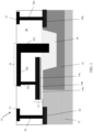
- FIG. 1 shows a transistor with a metal plate contact and respective manufacturing processes in accordance with aspects of the present disclosure.
- the structure 10 of FIG. 1 includes a gate structure 14 over a semiconductor substrate 12.
- the gate structure 14 may be representative of an LDMOS.
- the semiconductor substrate 12 may be composed of any suitable bulk material including, but not limited to, Si, SiGe, SiGeC, SiC, GaAs, InAs, InP, and other III/V or II/VI compound semiconductors.
- the semiconductor substrate 12 may comprise a p-type Si substrate or a p-well in the semiconductor substate 12.
- the semiconductor substrate 12 may also be semiconductor-on-insulator (SOI) technology.
- SOI semiconductor-on-insulator
- the gate structure 14 may be provided over an N-well 16 and a shallow trench isolation structure 18. As described with respect to FIG. 3A , the gate structure 14 may be fabricated using deposition, lithography and etching processes as is known in the art.
- the shallow trench isolation structure 18 can be formed by conventional lithography, etching and deposition methods known to those of skill in the art as also described in FIG. 3A .
- the gate structure 14 may include gate dielectric materials 14a, 14b and a gate electrode 14c.
- the gate dielectric materials 14a, 14b may be a combination of SiO 2 and a high-k dielectric material, respectively.
- the gate dielectric material 14a may be the same insulator material as the insulator material of the shallow trench isolation structure 18.
- the high-k dielectric gate material 14b may be, e.g., HfO 2 Al 2 O 3 , Ta 2 O 3 , TiO 2 , La 2 O 3 , SrTiO 3 , LaAlO 3 , ZrO 2 , Y 2 O 3 , Gd 2 O 3 , and combinations including multilayers thereof.
- the gate electrode 14c may be metal material or polysilicon material.
- the metal material may be workfunction materials such as, e.g., Ti, TiAlC, Al, TiAl, TaN, TiN, TiC, HfTi, TiSi, TaSi, TaC and/or Co
- Diffusion regions (e.g., source and drain regions) 20, 20a may be provided adjacent to the gate structure 14.
- the diffusion regions 20, 20a may be n-type diffusion regions for source and drain regions.
- the diffusion regions 20, 20a may be respectively connected to a source contact (interconnect) 24 and a drain contact (interconnect) 24a.
- a wiring structure 27 may be electrically connected to each of the source contact 24 and the drain contact 24a.
- the source contact 24 and drain contact 24a may be on a same back end of the line wiring layer, e.g., CA level.
- the wiring structure 27 may be on a same level, e.g., M1 level, as a wiring structure 22b of a gate contact 22.
- the diffusion regions 20, 20a and the N-well 16 may be formed by a conventional ion implantation process that introduces a concentration of n-type dopant into the semiconductor substrate 12 as described in FIG. 3A .
- the drain region 20a may be formed in the N-well 16, adjacent to the shallow trench isolation structure 18.
- the source contact 24, the drain contact 24a and wiring structures 27 may be provided in interlevel dielectric material 26.
- the interlevel dielectric material 26 may include layers of oxide and nitride, as an illustrative, non-limiting example.
- a gate contact 22 is electrically (e.g., directly) connected to the gate structure 14.
- the gate contact 22 may be provided in the interlevel dielectric material 26 and may include an interconnect contact 22a, a wiring structure 22b and a metal field plate 22c extending into the shallow trench isolation structure 18.
- the interconnect contact 22a and the metal field plate 22c may be on a same wiring level with the wiring structure 22b, which are also both connected to the wiring structure 22b. In this way, each part of the gate contact 22 is electrically connected to the gate structure 14.
- the gate contact 22 may comprise metal material such as, e.g., aluminum, copper, tungsten or other back end of the line conductive material.
- the shallow trench isolation structure 18 may define a drift region between an edge of the gate structure 14 and a drain region, e.g., diffusion region 20a.
- the depth and width of the metal field plate 22c extending into the shallow trench isolation structure 18 may be adjusted to optimize device performance.
- the metal field plate 22c may extend deeply into the shallow trench isolation structure 18 without reaching or contacting the N-well 16, i.e., insulator material of the shallow trench isolation structure will electrically isolate the metal field plate 22c from the N-well 16.
- the metal field plate 22c may attract electrons close to the interface of the shallow trench isolation structure 18 and the diffusion region 20a. Due to this attraction of electrons within the shallow trench isolation structure 18, for example, applying a positive bias to the gate structure 14 will reduce resistance in the drift region which, in turn, improves transconductance (gm), Ron and breakdown voltage, and reduces leakage.
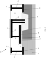
- FIG. 2 shows a structure in accordance with additional aspects of the present disclosure. More particularly, the structure 10a of FIG. 2 includes a contact 22 provided to the gate structure 14 and which comprises two metal field plates 22c' extending into the shallow trench isolation structure 18. The remaining features of the structure 10a are similar to the structure 10 of FIG. 1 .
- the metal field plates 22c' may attract electrons close to the interface of the shallow trench isolation structure 18 and the diffusion region 20a by applying a positive bias to the gate structure which, in turn, will reduce resistance in the drift region thereby improving transconductance (gm), Ron and breakdown voltage (by reducing the electric field), and reduces leakage.
- FIGS. 3A-3C show processing steps for the fabrication of the structure 10 shown in FIG. 1 . It should be recognized that the processing steps shown in FIGS. 3A-3C may also be used to fabricate the structure 10a shown in FIG. 2 , noting that an additional trench may be formed extending into the shallow trench isolation structure 18.
- the shallow trench isolation structure 18 can be formed in the semiconductor substrate 12 by using conventional lithography, etching and deposition methods. For example, a resist formed over the semiconductor substrate 12 is exposed to energy (light) and developed utilizing a conventional resist developer to form a pattern (opening). An etching process with a selective chemistry, e.g., reactive ion etching (RIE), will be used to transfer the pattern from the resist to the semiconductor substrate 12 to form a trench in the semiconductor substrate 12.
- insulator material e.g., SiO 2
- CVD chemical vapor deposition
- Additional insulator material e.g., SiO 2
- the diffusion regions 20, 20a and the N-well 16 may be formed by a conventional ion implantation process that introduces a concentration of n-type dopant into the semiconductor substrate 12.
- respective patterned implantation masks may be used to define selected areas exposed for the implantations.
- the implantation mask used to select the exposed area for forming the N-well 16 may be stripped after implantation, and before deposition of the implantation mask used to form the diffusion regions 20, 20a.
- the implantation masks may include a layer of a light-sensitive material, such as an organic photoresist, applied by a spin coating process, pre-baked, exposed to light projected through a photomask, baked after exposure, and developed with a chemical developer.
- Each of the implantation masks has a thickness and stopping power sufficient to block masked areas against receiving a dose of the implanted ions.
- the n-type dopants may be, e.g., Arsenic (As), Phosphorus (P) and Sb, among other suitable examples.
- the gate structure 14 may be formed by conventional deposition and patterning processes.
- the gate dielectric materials 14a, 14b and the gate electrode 14c may be deposited by conventional atomic layer deposition (ALD) processes or plasma enhanced CVD (PECVD) processes; whereas the gate electrode 14 may be deposited by a CVD process.
- the gate dielectric material 14a may be deposited at the same time and with the same insulator material of forming the shallow trench isolation structure 18, e.g., using a CVD process.
- the materials 14a, 14b, 14c may be patterned using conventional lithography and etching processes, with the gate structure 14 extending over the shallow trench isolation structure 18, the N-well 16 and p-type semiconductor substrate 12.
- Sidewall spacers may be formed on the gate structure by a deposition of insulator material, e.g., oxide and/or nitride, followed by an anisotropic etching process as is known in the art.
- the diffusion regions 20, 20a may be formed after the gate structure 14.
- the interlevel dielectric material 26 is deposited over the gate structure 14 and diffusion regions 20, 20a.
- the interlevel dielectric material 26 may be alternating layers of SiO 2 and nitride, deposited by a conventional deposition method, e.g., CVD.
- Contact holes 28, 28a may be etched into the interlevel dielectric material 26.
- the contact holes 28 may be etched to expose the gate electrode 14a and diffusion regions 20, 20a; whereas the contact hole 28a may be etched deeply into the shallow trench isolation structure 18.
- the etching process may include, e.g.: (i) a pre-etch with a deep hole for the contact hole 28a, and then patterning of the contact holes 28, with the contact hole 28a being etched into the shallow trench isolation structure 18; (ii) using a RIE that is super selective to silicide or polysilicon or metal which will stop on the gate structure 14 and diffusion regions 20, 20a and continue into the shallow trench isolation structure 18; or (iii) use two separate RIE steps (e.g., one for the deeper hole 28a and the other etch for the contact holes 28).
- the contacts 22, 22c, 24, 24a are formed by depositing metal material within the contact holes 28, 28a.
- the metal material may be, for example, aluminum, copper, tungsten or other back end of the line conductive material.
- the metal material may be deposited by a conventional deposition process, e.g., CVD, followed by a planarization process to remove any excess material on a surface of the interlevel dielectric material.
- the planarization process may be a chemical mechanical polishing (CMP) process.
- a silicide contact may be provided on the polysilicon material of the gate structure 14 and the diffusion regions 20, 20a.
- the silicide process begins with deposition of a thin transition metal layer, e.g., nickel, cobalt or titanium, over fully formed and patterned semiconductor devices (e.g., doped or ion implanted source region 20and drain region 20a and respective device 14). After deposition of the material, the structure is heated allowing the transition metal to react with exposed silicon (or other semiconductor material as described herein) in the active regions of the semiconductor device (e.g., source, drain, gate contact region) forming a low-resistance transition metal silicide.
- a thin transition metal layer e.g., nickel, cobalt or titanium
- any remaining transition metal is removed by chemical etching, leaving silicide contacts in the active regions of the device. It should be understood by those of skill in the art that silicide contacts would not be required on the devices when the gate structure is composed of a metal material.
- wiring structures 27 may be formed to the source and drain contacts 24, 24a, and the wiring structure 22b may be formed connected to the gate contact 22a to the metal field plate 22c.
- the wiring structures 27, 22b may be formed by depositing additional layer(s) of interlevel dielectric material on the interlevel dielectric material, followed by a patterning process to form trenches exposing the contacts 24, 24a, 22a and metal field plate 22c.
- a metal material may be deposited within the trenches, followed by a CMP process.
- the additional layer(s) of interlevel dielectric material and the metal material may be deposited by conventional CVD processes.
- the additional layer(s) of interlevel dielectric material may be SiO 2 and/or nitride and the metal material may be similar or the same as the metal material used for the contacts 24, 24a, 22a and field plate 22c.
- the transistor can be utilized in system on chip (SoC) technology.
- SoC system on chip
- the SoC is an integrated circuit (also known as a "chip") that integrates all components of an electronic system on a single chip or substrate. As the components are integrated on a single substrate, SoCs consume much less power and take up much less area than multichip designs with equivalent functionality. Because of this, SoCs are becoming the dominant force in the mobile computing (such as in Smartphones) and edge computing markets. SoC is also used in embedded systems and the Internet of Things.
- the method(s) as described above is used in the fabrication of integrated circuit chips.
- the resulting integrated circuit chips can be distributed by the fabricator in raw wafer form (that is, as a single wafer that has multiple unpackaged chips), as a bare die, or in a packaged form.
- the chip is mounted in a single chip package (such as a plastic carrier, with leads that are affixed to a motherboard or other higher level carrier) or in a multichip package (such as a ceramic carrier that has either or both surface interconnections or buried interconnections).
- the chip is then integrated with other chips, discrete circuit elements, and/or other signal processing devices as part of either (a) an intermediate product, such as a motherboard, or (b) an end product.
- the end product can be any product that includes integrated circuit chips, ranging from toys and other low-end applications to advanced computer products having a display, a keyboard or other input device, and a central processor.
Landscapes
- Insulated Gate Type Field-Effect Transistor (AREA)
- Electrodes Of Semiconductors (AREA)
- Engineering & Computer Science (AREA)
- Manufacturing & Machinery (AREA)
Abstract
Description
- The present disclosure relates to semiconductor structures and, more particularly, to a transistor with a metal field plate contact and methods of manufacture.
- A laterally-diffused metal-oxide semiconductor (LDMOS) is a planar doublediffused MOSFET (metal-oxide-semiconductor field-effect transistor) used in amplifiers, including microwave power amplifiers, RF power amplifiers and audio power amplifiers. The fabrication of LDMOS devices mostly involves various ion-implantation and subsequent annealing cycles. As an example, the drift region of a power MOSFET is fabricated using up to three ion implantation sequences in order to achieve the appropriate doping profile needed to withstand high electric fields.
- A silicon-based RF LDMOS (radio-frequency LDMOS) is a widely used RF power amplifier in mobile networks, enabling the majority of the world's cellular voice and data traffic. LDMOS devices are widely used in RF power amplifiers for basestations as the requirement is for high output power with a corresponding drain to source breakdown voltage. Compared to other devices such as GaAs FETs, RF LDMOS shows a lower maximum power gain frequency.
- In an aspect of the disclosure, a structure comprises: a gate structure on a semiconductor substrate; a shallow trench isolation structure within the semiconductor substrate; and a contact extending from the gate structure and into the shallow trench isolation structure.
Additional features of the structure are set forth in dependent claims 2 to 9. - In an aspect of the disclosure, a structure comprises: a semiconductor substrate; a shallow trench isolation structure within the semiconductor substrate; a gate structure extending partially over the shallow trench isolation structure; a drain diffusion adjacent to the shallow trench isolation structure; and a contact electrically connected to the gate structure and extending within the shallow trench isolation structure between the drain diffusion and the gate structure.
Additional features of the structure are set forth in dependent claims 11 to 14 - In an aspect of the disclosure, a method comprises: forming a gate structure on a semiconductor substrate; forming a shallow trench isolation structure within the semiconductor substrate; and forming a contact extending from the gate structure and into the shallow trench isolation structure.
- The present disclosure is described in the detailed description which follows, in reference to the noted plurality of drawings by way of non-limiting examples of exemplary embodiments of the present disclosure.
-
FIG. 1 shows a transistor with a metal plate contact and methods of manufacture in accordance with aspects of the present disclosure. -
FIG. 2 shows a transistor with a metal plate contact in accordance with additional aspects of the present disclosure. -
FIGS. 3A-3C show processing steps for the fabrication of the transistor with the metal plate contact shown inFIG. 1 , in accordance with aspects of the present disclosure. - The present disclosure relates to semiconductor structures and, more particularly, to a transistor with a metal field plate contact and methods of manufacture. More specifically, the present disclosure relates to a laterally diffused metal oxide semiconductor (LDMOS) with a metal field plate extending within a shallow trench isolation structure. Advantageously, the metal field plate provides improved performance of the LDMOS.
- The transistor of the present disclosure can be manufactured in a number of ways using a number of different tools. In general, though, the methodologies and tools are used to form structures with dimensions in the micrometer and nanometer scale. The methodologies, i.e., technologies, employed to manufacture the transistor of the present disclosure have been adopted from integrated circuit (IC) technology. For example, the structures are built on wafers and are realized in films of material patterned by photolithographic processes on the top of a wafer. In particular, the fabrication of the transistor uses three basic building blocks: (i) deposition of thin films of material on a substrate, (ii) applying a patterned mask on top of the films by photolithographic imaging, and (iii) etching the films selectively to the mask. In addition, precleaning processes may be used to clean etched surfaces of any contaminants, as is known in the art. Moreover, when necessary, rapid thermal anneal processes may be used to drive-in dopants or material layers as is known in the art.
-
FIG. 1 shows a transistor with a metal plate contact and respective manufacturing processes in accordance with aspects of the present disclosure. More particularly, thestructure 10 ofFIG. 1 includes agate structure 14 over asemiconductor substrate 12. In embodiments, thegate structure 14 may be representative of an LDMOS. Thesemiconductor substrate 12 may be composed of any suitable bulk material including, but not limited to, Si, SiGe, SiGeC, SiC, GaAs, InAs, InP, and other III/V or II/VI compound semiconductors. Preferably, thesemiconductor substrate 12 may comprise a p-type Si substrate or a p-well in thesemiconductor substate 12. Thesemiconductor substrate 12 may also be semiconductor-on-insulator (SOI) technology. - In embodiments, the
gate structure 14 may be provided over an N-well 16 and a shallowtrench isolation structure 18. As described with respect toFIG. 3A , thegate structure 14 may be fabricated using deposition, lithography and etching processes as is known in the art. The shallowtrench isolation structure 18 can be formed by conventional lithography, etching and deposition methods known to those of skill in the art as also described inFIG. 3A . - The
gate structure 14 may include gatedielectric materials gate electrode 14c. The gatedielectric materials dielectric material 14a may be the same insulator material as the insulator material of the shallowtrench isolation structure 18. The high-kdielectric gate material 14b may be, e.g., HfO2 Al2O3, Ta2O3, TiO2, La2O3, SrTiO3, LaAlO3, ZrO2, Y2O3, Gd2O3, and combinations including multilayers thereof. Thegate electrode 14c may be metal material or polysilicon material. The metal material may be workfunction materials such as, e.g., Ti, TiAlC, Al, TiAl, TaN, TiN, TiC, HfTi, TiSi, TaSi, TaC and/or Co. - Diffusion regions (e.g., source and drain regions) 20, 20a may be provided adjacent to the
gate structure 14. Thediffusion regions diffusion regions wiring structure 27 may be electrically connected to each of thesource contact 24 and thedrain contact 24a. The source contact 24 and drain contact 24a may be on a same back end of the line wiring layer, e.g., CA level. Thewiring structure 27 may be on a same level, e.g., M1 level, as awiring structure 22b of agate contact 22. - The
diffusion regions well 16 may be formed by a conventional ion implantation process that introduces a concentration of n-type dopant into thesemiconductor substrate 12 as described inFIG. 3A . Thedrain region 20a may be formed in the N-well 16, adjacent to the shallowtrench isolation structure 18. The source contact 24, the drain contact 24a andwiring structures 27 may be provided in interleveldielectric material 26. The interleveldielectric material 26 may include layers of oxide and nitride, as an illustrative, non-limiting example. - Still referring to
FIG. 1 , agate contact 22 is electrically (e.g., directly) connected to thegate structure 14. In embodiments, thegate contact 22 may be provided in the interleveldielectric material 26 and may include aninterconnect contact 22a, awiring structure 22b and ametal field plate 22c extending into the shallowtrench isolation structure 18. The interconnect contact 22a and themetal field plate 22c may be on a same wiring level with thewiring structure 22b, which are also both connected to thewiring structure 22b. In this way, each part of thegate contact 22 is electrically connected to thegate structure 14. Thegate contact 22 may comprise metal material such as, e.g., aluminum, copper, tungsten or other back end of the line conductive material. - In embodiments, the shallow
trench isolation structure 18 may define a drift region between an edge of thegate structure 14 and a drain region, e.g.,diffusion region 20a. The depth and width of themetal field plate 22c extending into the shallowtrench isolation structure 18 may be adjusted to optimize device performance. For example, in embodiments, themetal field plate 22c may extend deeply into the shallowtrench isolation structure 18 without reaching or contacting the N-well 16, i.e., insulator material of the shallow trench isolation structure will electrically isolate themetal field plate 22c from the N-well 16. - In operation, the
metal field plate 22c may attract electrons close to the interface of the shallowtrench isolation structure 18 and thediffusion region 20a. Due to this attraction of electrons within the shallowtrench isolation structure 18, for example, applying a positive bias to thegate structure 14 will reduce resistance in the drift region which, in turn, improves transconductance (gm), Ron and breakdown voltage, and reduces leakage. -
FIG. 2 shows a structure in accordance with additional aspects of the present disclosure. More particularly, the structure 10a ofFIG. 2 includes acontact 22 provided to thegate structure 14 and which comprises twometal field plates 22c' extending into the shallowtrench isolation structure 18. The remaining features of the structure 10a are similar to thestructure 10 ofFIG. 1 . Again, in operation, themetal field plates 22c' may attract electrons close to the interface of the shallowtrench isolation structure 18 and thediffusion region 20a by applying a positive bias to the gate structure which, in turn, will reduce resistance in the drift region thereby improving transconductance (gm), Ron and breakdown voltage (by reducing the electric field), and reduces leakage. -
FIGS. 3A-3C show processing steps for the fabrication of thestructure 10 shown inFIG. 1 . It should be recognized that the processing steps shown inFIGS. 3A-3C may also be used to fabricate the structure 10a shown inFIG. 2 , noting that an additional trench may be formed extending into the shallowtrench isolation structure 18. - As shown in
FIG. 3A , the shallowtrench isolation structure 18 can be formed in thesemiconductor substrate 12 by using conventional lithography, etching and deposition methods. For example, a resist formed over thesemiconductor substrate 12 is exposed to energy (light) and developed utilizing a conventional resist developer to form a pattern (opening). An etching process with a selective chemistry, e.g., reactive ion etching (RIE), will be used to transfer the pattern from the resist to thesemiconductor substrate 12 to form a trench in thesemiconductor substrate 12. Following the resist removal by a conventional oxygen ashing process or other known stripants, insulator material (e.g., SiO2) can be deposited by any conventional deposition processes, e.g., chemical vapor deposition (CVD) processes. Additional insulator material (e.g., SiO2) may be deposited and patterned on the surface of thesemiconductor substrate 12 to form thegate dielectric material 14a. - The
diffusion regions semiconductor substrate 12. In embodiments, respective patterned implantation masks may be used to define selected areas exposed for the implantations. The implantation mask used to select the exposed area for forming the N-well 16 may be stripped after implantation, and before deposition of the implantation mask used to form thediffusion regions - The
gate structure 14 may be formed by conventional deposition and patterning processes. For example, thegate dielectric materials gate electrode 14c may be deposited by conventional atomic layer deposition (ALD) processes or plasma enhanced CVD (PECVD) processes; whereas thegate electrode 14 may be deposited by a CVD process. In embodiments, thegate dielectric material 14a may be deposited at the same time and with the same insulator material of forming the shallowtrench isolation structure 18, e.g., using a CVD process. Following the deposition processes, thematerials gate structure 14 extending over the shallowtrench isolation structure 18, the N-well 16 and p-type semiconductor substrate 12. Sidewall spacers may be formed on the gate structure by a deposition of insulator material, e.g., oxide and/or nitride, followed by an anisotropic etching process as is known in the art. In embodiments, thediffusion regions gate structure 14. - In
FIG. 3B , the interleveldielectric material 26 is deposited over thegate structure 14 anddiffusion regions dielectric material 26 may be alternating layers of SiO2 and nitride, deposited by a conventional deposition method, e.g., CVD. - Contact holes 28, 28a may be etched into the interlevel
dielectric material 26. In embodiments, the contact holes 28 may be etched to expose thegate electrode 14a anddiffusion regions contact hole 28a may be etched deeply into the shallowtrench isolation structure 18. In embodiments, the etching process may include, e.g.: (i) a pre-etch with a deep hole for thecontact hole 28a, and then patterning of the contact holes 28, with thecontact hole 28a being etched into the shallowtrench isolation structure 18; (ii) using a RIE that is super selective to silicide or polysilicon or metal which will stop on thegate structure 14 anddiffusion regions trench isolation structure 18; or (iii) use two separate RIE steps (e.g., one for thedeeper hole 28a and the other etch for the contact holes 28). - In
FIG. 3C , thecontacts - As should be understood by those of skill in the art, prior to the deposition of the metal material, a silicide contact may be provided on the polysilicon material of the
gate structure 14 and thediffusion regions region 20a and respective device 14). After deposition of the material, the structure is heated allowing the transition metal to react with exposed silicon (or other semiconductor material as described herein) in the active regions of the semiconductor device (e.g., source, drain, gate contact region) forming a low-resistance transition metal silicide. Following the reaction, any remaining transition metal is removed by chemical etching, leaving silicide contacts in the active regions of the device. It should be understood by those of skill in the art that silicide contacts would not be required on the devices when the gate structure is composed of a metal material. - Referring back to
FIG. 1 ,wiring structures 27 may be formed to the source anddrain contacts wiring structure 22b may be formed connected to thegate contact 22a to themetal field plate 22c. Thewiring structures contacts metal field plate 22c. A metal material may be deposited within the trenches, followed by a CMP process. In embodiments, the additional layer(s) of interlevel dielectric material and the metal material may be deposited by conventional CVD processes. The additional layer(s) of interlevel dielectric material may be SiO2 and/or nitride and the metal material may be similar or the same as the metal material used for thecontacts field plate 22c. - The transistor can be utilized in system on chip (SoC) technology. The SoC is an integrated circuit (also known as a "chip") that integrates all components of an electronic system on a single chip or substrate. As the components are integrated on a single substrate, SoCs consume much less power and take up much less area than multichip designs with equivalent functionality. Because of this, SoCs are becoming the dominant force in the mobile computing (such as in Smartphones) and edge computing markets. SoC is also used in embedded systems and the Internet of Things.
- The method(s) as described above is used in the fabrication of integrated circuit chips. The resulting integrated circuit chips can be distributed by the fabricator in raw wafer form (that is, as a single wafer that has multiple unpackaged chips), as a bare die, or in a packaged form. In the latter case the chip is mounted in a single chip package (such as a plastic carrier, with leads that are affixed to a motherboard or other higher level carrier) or in a multichip package (such as a ceramic carrier that has either or both surface interconnections or buried interconnections). In any case the chip is then integrated with other chips, discrete circuit elements, and/or other signal processing devices as part of either (a) an intermediate product, such as a motherboard, or (b) an end product. The end product can be any product that includes integrated circuit chips, ranging from toys and other low-end applications to advanced computer products having a display, a keyboard or other input device, and a central processor.
- The descriptions of the various embodiments of the present disclosure have been presented for purposes of illustration, but are not intended to be exhaustive or limited to the embodiments disclosed. Many modifications and variations will be apparent to those of ordinary skill in the art without departing from the scope and spirit of the described embodiments. The terminology used herein was chosen to best explain the principles of the embodiments, the practical application or technical improvement over technologies found in the marketplace, or to enable others of ordinary skill in the art to understand the embodiments disclosed herein.
Claims (15)
- A structure comprising:a gate structure on a semiconductor substrate;a shallow trench isolation structure within the semiconductor substrate; anda contact extending from the gate structure and into the shallow trench isolation structure.
- The structure of claim 1, wherein the gate structure partially extends over the shallow trench isolation structure.
- The structure of claim 1, wherein the contact comprises a gate contact, a wiring structure and a metal field plate that extends into the shallow trench isolation structure.
- The structure of claim 3, wherein the metal field plate comprises a single interconnect structure or a plurality of interconnect structures each electrically connected to the gate structure and which extends into the shallow trench isolation structure.
- The structure of claim 2, further comprising a drain diffusion separated from the gate structure by the shallow trench isolation structure, wherein the contact optionally extends between an edge of the gate structure and the drain diffusion.
- The structure of one of claims 1 to 5, wherein the gate structure comprises a laterally diffused metal oxide semiconductor (LDMOS) device.
- The structure of one of claims 1 to 6, wherein the gate structure includes a gate dielectric material, which comprises a same insulator material as the shallow trench isolation structure, wherein the gate dielectric material optionally extends over an N-well and the shallow trench isolation structure.
- The structure of claim 7, wherein the shallow trench isolation structure is within the N-well.
- The structure of claim 8, wherein the contact which extends into the shallow trench isolation structure is separated from the N-well by insulator material of the shallow trench isolation structure.
- A structure comprising:a semiconductor substrate;a shallow trench isolation structure within the semiconductor substrate;a gate structure extending partially over the shallow trench isolation structure;a drain diffusion adjacent to the shallow trench isolation structure; anda contact electrically connected to the gate structure and extending within the shallow trench isolation structure between the drain diffusion and the gate structure.
- The structure of claim 10, wherein the contact comprises a gate contact, a wiring structure and a metal field plate, the metal field plate extends into the shallow trench isolation structure.
- The structure of claim 10 or 11, wherein the metal field plate comprises a single interconnect structure or two interconnect structures.
- The structure of one of claims 10 to 12, wherein the gate structure comprises a laterally diffused metal oxide semiconductor (LDMOS) device.
- The structure of one of claims 10 to 13, wherein the gate structure includes a gate dielectric material, and the gate dielectric material and the shallow trench isolation structure comprise a same insulator material, wherein the shallow trench isolation structure is optionally within an N-well and the gate dielectric material optionally extends over the N-well and the shallow trench isolation structure.
- A method comprising:forming a gate structure on a semiconductor substrate;forming a shallow trench isolation structure within the semiconductor substrate; andforming a contact extending from the gate structure and into the shallow trench isolation structure.
Applications Claiming Priority (1)
| Application Number | Priority Date | Filing Date | Title |
|---|---|---|---|
| US17/984,736 US12648172B2 (en) | 2022-11-10 | 2022-11-10 | Transistor with metal field plate contact |
Publications (1)
| Publication Number | Publication Date |
|---|---|
| EP4369408A1 true EP4369408A1 (en) | 2024-05-15 |
Family
ID=88146992
Family Applications (1)
| Application Number | Title | Priority Date | Filing Date |
|---|---|---|---|
| EP23198686.0A Pending EP4369408A1 (en) | 2022-11-10 | 2023-09-21 | Transistor with metal field plate contact |
Country Status (3)
| Country | Link |
|---|---|
| US (1) | US12648172B2 (en) |
| EP (1) | EP4369408A1 (en) |
| CN (1) | CN118016712A (en) |
Families Citing this family (5)
| Publication number | Priority date | Publication date | Assignee | Title |
|---|---|---|---|---|
| KR102749671B1 (en) * | 2023-01-11 | 2025-01-03 | 에스케이키파운드리 주식회사 | Semiconductor device and method of manufacturing the same |
| CN117855283B (en) * | 2024-03-08 | 2024-05-17 | 粤芯半导体技术股份有限公司 | A LDMOS device and a method for manufacturing the same |
| US12310047B1 (en) | 2024-10-07 | 2025-05-20 | Globalfoundries Singapore Pte. Ltd. | Laterally-diffused metal-oxide-semiconductor devices with a field plate |
| CN121310568B (en) * | 2025-12-08 | 2026-03-24 | 芯联集成电路制造股份有限公司 | High-voltage semiconductor device and method for manufacturing the same |
| CN121865673A (en) * | 2026-03-17 | 2026-04-14 | 合肥晶合集成电路股份有限公司 | Manufacturing method of metal field plate |
Citations (2)
| Publication number | Priority date | Publication date | Assignee | Title |
|---|---|---|---|---|
| US20140061791A1 (en) * | 2012-08-28 | 2014-03-06 | United Microelectronics Corp. | Mos transistor |
| US20170104097A1 (en) * | 2015-10-07 | 2017-04-13 | SK Hynix Inc. | Lateral high voltage integrated devices having trencn insulation field plates and metal field plates |
Family Cites Families (89)
| Publication number | Priority date | Publication date | Assignee | Title |
|---|---|---|---|---|
| US5930633A (en) * | 1997-07-23 | 1999-07-27 | Taiwan Semiconductor Manufacturing Company, Ltd. | Integrated butt-contact process in shallow trench isolation |
| US6114205A (en) * | 1998-10-30 | 2000-09-05 | Sony Corporation | Epitaxial channel vertical MOS transistor |
| US7576388B1 (en) * | 2002-10-03 | 2009-08-18 | Fairchild Semiconductor Corporation | Trench-gate LDMOS structures |
| US7122876B2 (en) * | 2004-08-11 | 2006-10-17 | Taiwan Semiconductor Manufacturing Company, Ltd. | Isolation-region configuration for integrated-circuit transistor |
| EP1717850A1 (en) * | 2005-04-29 | 2006-11-02 | STMicroelectronics S.r.l. | Method of manufacturing a lateral power MOS transistor |
| US7368785B2 (en) * | 2005-05-25 | 2008-05-06 | United Microelectronics Corp. | MOS transistor device structure combining Si-trench and field plate structures for high voltage device |
| US8026146B2 (en) * | 2006-08-31 | 2011-09-27 | Nxp B.V. | Method of manufacturing a bipolar transistor |
| US8035140B2 (en) * | 2007-07-26 | 2011-10-11 | Infineon Technologies Ag | Method and layout of semiconductor device with reduced parasitics |
| US7956412B2 (en) * | 2007-12-04 | 2011-06-07 | International Business Machines Corporation | Lateral diffusion field effect transistor with a trench field plate |
| KR20090072013A (en) * | 2007-12-28 | 2009-07-02 | 주식회사 동부하이텍 | Horizontal Dimos Transistor |
| US7888732B2 (en) * | 2008-04-11 | 2011-02-15 | Texas Instruments Incorporated | Lateral drain-extended MOSFET having channel along sidewall of drain extension dielectric |
| US8174071B2 (en) * | 2008-05-02 | 2012-05-08 | Taiwan Semiconductor Manufacturing Co., Ltd. | High voltage LDMOS transistor |
| JP5385679B2 (en) * | 2008-05-16 | 2014-01-08 | 旭化成エレクトロニクス株式会社 | Lateral semiconductor device and manufacturing method thereof |
| US7851857B2 (en) * | 2008-07-30 | 2010-12-14 | Freescale Semiconductor, Inc. | Dual current path LDMOSFET with graded PBL for ultra high voltage smart power applications |
| DE102008051245B4 (en) * | 2008-10-10 | 2015-04-02 | Austriamicrosystems Ag | High-voltage transistor with high current carrying capacity and method of manufacture |
| US7786507B2 (en) * | 2009-01-06 | 2010-08-31 | Texas Instruments Incorporated | Symmetrical bi-directional semiconductor ESD protection device |
| US8643090B2 (en) * | 2009-03-23 | 2014-02-04 | Infineon Technologies Ag | Semiconductor devices and methods for manufacturing a semiconductor device |
| US8004039B2 (en) * | 2009-07-31 | 2011-08-23 | Micrel, Inc. | Field effect transistor with trench-isolated drain |
| US8513712B2 (en) * | 2009-09-28 | 2013-08-20 | Taiwan Semiconductor Manufacturing Company, Ltd. | Method and apparatus for forming a semiconductor gate |
| KR20110079021A (en) | 2009-12-31 | 2011-07-07 | 주식회사 동부하이텍 | Semiconductor device and manufacturing method thereof |
| US8227858B2 (en) * | 2010-01-11 | 2012-07-24 | Excelliance Mos Corporation | Power MOSFET |
| JP5404550B2 (en) * | 2010-07-29 | 2014-02-05 | 株式会社東芝 | Semiconductor device manufacturing method and semiconductor device |
| US20120094457A1 (en) * | 2010-10-14 | 2012-04-19 | Ann Gabrys | Sti-aligned ldmos drift implant to enhance manufacturability while optimizing rdson and safe operating area |
| TWI408811B (en) * | 2011-02-25 | 2013-09-11 | 立錡科技股份有限公司 | High voltage component and method of manufacturing same |
| US9343538B2 (en) * | 2011-05-13 | 2016-05-17 | Richtek Technology Corporation | High voltage device with additional isolation region under gate and manufacturing method thereof |
| US8436418B2 (en) * | 2011-06-20 | 2013-05-07 | United Microelectronics Corp. | High-voltage semiconductor device with electrostatic discharge protection |
| US8716791B1 (en) * | 2011-08-11 | 2014-05-06 | Maxim Integrated Products, Inc. | LDMOS with corrugated drift region |
| CN103311247B (en) * | 2012-03-14 | 2016-07-13 | 中国科学院微电子研究所 | Semiconductor device and manufacturing method thereof |
| US20130277741A1 (en) * | 2012-04-23 | 2013-10-24 | Globalfoundries Singapore Pte Ltd | Ldmos device with field effect structure to control breakdown voltage, and methods of making such a device |
| US8766358B2 (en) * | 2012-04-24 | 2014-07-01 | United Microelectronics Corp. | Semiconductor structure and method for manufacturing the same |
| US8987813B2 (en) * | 2012-08-10 | 2015-03-24 | United Microelectronics Corp. | High voltage metal-oxide-semiconductor transistor device |
| US9082846B2 (en) * | 2013-04-25 | 2015-07-14 | Globalfoundries Singapore Pte. Ltd. | Integrated circuits with laterally diffused metal oxide semiconductor structures |
| US8896057B1 (en) * | 2013-05-14 | 2014-11-25 | United Microelectronics Corp. | Semiconductor structure and method for manufacturing the same |
| US8981475B2 (en) * | 2013-06-18 | 2015-03-17 | International Business Machines Corporation | Lateral diffusion metal oxide semiconductor (LDMOS) |
| US8994103B2 (en) * | 2013-07-10 | 2015-03-31 | United Microelectronics Corp. | High voltage metal-oxide-semiconductor transistor device and manufacturing method thereof |
| US9306034B2 (en) * | 2014-02-24 | 2016-04-05 | Vanguard International Semiconductor Corporation | Method and apparatus for power device with multiple doped regions |
| JP6279346B2 (en) * | 2014-02-27 | 2018-02-14 | ルネサスエレクトロニクス株式会社 | Semiconductor device |
| US9306013B2 (en) * | 2014-05-23 | 2016-04-05 | Texas Instruments Incorporated | Method of forming a gate shield in an ED-CMOS transistor and a base of a bipolar transistor using BICMOS technologies |
| CN105206665A (en) * | 2014-05-27 | 2015-12-30 | 中芯国际集成电路制造(上海)有限公司 | Semiconductor device, manufacturing method thereof and electronic device |
| US9443958B2 (en) * | 2014-10-06 | 2016-09-13 | United Microelectronics Corp. | High voltage metal-oxide-semiconductor transistor device and method of forming the same |
| US9842903B2 (en) * | 2014-10-20 | 2017-12-12 | Globalfoundries Singapore Pte. Ltd. | Integrated circuits with laterally diffused metal oxide semiconductor structures and methods for fabricating the same |
| US10756208B2 (en) * | 2014-11-25 | 2020-08-25 | Taiwan Semiconductor Manufacturing Co., Ltd. | Integrated chip and method of forming the same |
| US9590053B2 (en) * | 2014-11-25 | 2017-03-07 | Taiwan Semiconductor Manufacturing Co., Ltd. | Methodology and structure for field plate design |
| US20160211348A1 (en) * | 2015-01-21 | 2016-07-21 | Maxchip Electronics Corp. | Trench lateral diffusion metal oxide semiconductor device and manufacturing method of the same |
| CN106298912B (en) * | 2015-05-15 | 2020-06-30 | 联华电子股份有限公司 | Semiconductor structure and manufacturing method thereof |
| US9391196B1 (en) * | 2015-07-22 | 2016-07-12 | United Microelectronics Corp. | High-voltage metal-oxide-semiconductor transistor device and manufacturing method thereof |
| JP6509665B2 (en) * | 2015-07-23 | 2019-05-08 | ルネサスエレクトロニクス株式会社 | Semiconductor device |
| US9780207B2 (en) * | 2015-12-30 | 2017-10-03 | Globalfoundries Singapore Pte. Ltd. | Self-aligned high voltage LDMOS |
| CN107104137B (en) * | 2016-02-22 | 2021-11-02 | 联华电子股份有限公司 | Fin transistor element |
| US9954100B2 (en) * | 2016-03-24 | 2018-04-24 | Taiwan Semiconductor Manufacturing Company, Ltd. | Method and apparatus for high voltate transistors |
| US10825905B2 (en) * | 2016-06-01 | 2020-11-03 | Taiwan Semiconductor Manufacturing Co., Ltd. | Thin poly field plate design |
| US9871132B1 (en) * | 2016-08-15 | 2018-01-16 | Globalfoundries Singapore Pte. Ltd. | Extended drain metal-oxide-semiconductor transistor |
| JP6710627B2 (en) * | 2016-12-20 | 2020-06-17 | ルネサスエレクトロニクス株式会社 | Semiconductor device and manufacturing method thereof |
| CN108389906B (en) * | 2017-02-03 | 2023-01-10 | 联华电子股份有限公司 | High voltage metal oxide semiconductor transistor element |
| TWI724164B (en) * | 2017-05-05 | 2021-04-11 | 聯華電子股份有限公司 | Semiconductor device and method for fabricating the same |
| US10505038B2 (en) * | 2017-09-28 | 2019-12-10 | Taiwan Semiconductor Manufacturing Company Ltd. | Semiconductor structure and associated fabricating method |
| US10164006B1 (en) * | 2017-10-30 | 2018-12-25 | Globalfoundries Inc. | LDMOS FinFET structures with trench isolation in the drain extension |
| JP6971877B2 (en) * | 2018-02-20 | 2021-11-24 | ルネサスエレクトロニクス株式会社 | Semiconductor device |
| US10971624B2 (en) * | 2018-03-19 | 2021-04-06 | Macronix International Co., Ltd. | High-voltage transistor devices with two-step field plate structures |
| JP7040976B2 (en) * | 2018-03-29 | 2022-03-23 | ラピスセミコンダクタ株式会社 | Semiconductor device |
| CN110350032A (en) * | 2018-04-04 | 2019-10-18 | 无锡华润上华科技有限公司 | A kind of semiconductor devices |
| US10680100B2 (en) * | 2018-07-03 | 2020-06-09 | Taiwan Semiconductor Manufacturing Co., Ltd. | Field structure and methodology |
| CN110767740B (en) * | 2018-07-27 | 2021-10-15 | 无锡华润上华科技有限公司 | Semiconductor device and method of manufacturing the same |
| US11069804B2 (en) * | 2018-08-31 | 2021-07-20 | Alpha And Omega Semiconductor (Cayman) Ltd. | Integration of HVLDMOS with shared isolation region |
| CN110364567A (en) * | 2019-07-24 | 2019-10-22 | 上海华虹宏力半导体制造有限公司 | LDMOS device and method of forming the same |
| CN110391293A (en) * | 2019-07-29 | 2019-10-29 | 上海华虹宏力半导体制造有限公司 | LDMOSFET device and its manufacturing method |
| US20210074851A1 (en) * | 2019-09-05 | 2021-03-11 | Richtek Technology Corporation | High voltage device and manufacturing method thereof |
| US11121225B2 (en) * | 2019-11-01 | 2021-09-14 | Taiwan Semiconductor Manufacturing Company, Ltd. | Field plate structure to enhance transistor breakdown voltage |
| CN113130646B (en) * | 2019-12-30 | 2023-05-02 | 无锡华润上华科技有限公司 | Semiconductor device and manufacturing method thereof |
| US10944001B1 (en) * | 2020-01-06 | 2021-03-09 | Nxp Usa, Inc. | Deep trench and junction hybrid isolation |
| US10910478B1 (en) * | 2020-03-04 | 2021-02-02 | Shuming Xu | Metal-oxide-semiconductor field-effect transistor having enhanced high-frequency performance |
| US11411086B2 (en) * | 2020-03-17 | 2022-08-09 | Taiwan Semiconductor Manufacturing Company, Ltd. | Field plate and isolation structure for high voltage device |
| CN111653621A (en) * | 2020-05-25 | 2020-09-11 | 华虹半导体(无锡)有限公司 | LDMOS device and method of making the same |
| US11515416B2 (en) * | 2020-09-23 | 2022-11-29 | Nxp Usa, Inc. | Laterally-diffused metal-oxide semiconductor transistor and method therefor |
| EP4200911A4 (en) * | 2020-12-04 | 2025-01-08 | Amplexia, LLC | Ldmos with self-aligned body and hybrid source |
| CN112909095B (en) | 2021-01-21 | 2024-03-19 | 上海华虹宏力半导体制造有限公司 | LDMOS devices and process methods |
| US11705515B2 (en) * | 2021-03-05 | 2023-07-18 | Taiwan Semiconductor Manufacturing Company, Ltd. | Gate electrode extending into a shallow trench isolation structure in high voltage devices |
| CN115206802B (en) * | 2021-04-12 | 2025-11-04 | 联华电子股份有限公司 | Laterally diffused metal-oxide semiconductor devices and their fabrication methods |
| KR102824278B1 (en) * | 2021-04-16 | 2025-06-23 | 주식회사 디비하이텍 | Semiconductor device and manufacturing the same |
| US20230420464A1 (en) * | 2022-06-23 | 2023-12-28 | Taiwan Semiconductor Manufacturing Company, Ltd. | Semiconductor device and method of manufacturing the same |
| US12581673B2 (en) * | 2022-09-16 | 2026-03-17 | Taiwan Semiconductor Manufacturing Company Ltd. | Schottky diode and method for forming the same |
| US20240203815A1 (en) * | 2022-12-20 | 2024-06-20 | Intel Corporation | Layer transfer diode or thin-film resistor for gallium nitride (gan) integrated circuit technology |
| TW202447966A (en) * | 2023-05-26 | 2024-12-01 | 聯華電子股份有限公司 | Semiconductor device and method of fabricating the same |
| DE102023206017A1 (en) * | 2023-06-27 | 2025-01-02 | Infineon Technologies Ag | SEMICONDUCTOR DEVICE WITH A BIPOLAR TRANSISTOR |
| US20250089311A1 (en) * | 2023-09-08 | 2025-03-13 | Taiwan Semiconductor Manufacturing Company, Ltd. | High voltage mosfet using shallow-shallow trench isolation structure |
| TW202535184A (en) * | 2024-02-15 | 2025-09-01 | 聯華電子股份有限公司 | Semiconductor device and forming method thereof |
| US12289913B1 (en) * | 2024-04-22 | 2025-04-29 | Globalfoundries Singapore Pte. Ltd | Device with metal field plate extension |
| US12408373B1 (en) * | 2024-04-29 | 2025-09-02 | Globalfoundries Singapore Pte. Ltd. | Device with three dimensional channel |
| US20250338532A1 (en) * | 2024-04-30 | 2025-10-30 | Texas Instruments Incorporated | Ldmos nanosheet transistor including a nanosheet drift region field plate |
-
2022
- 2022-11-10 US US17/984,736 patent/US12648172B2/en active Active
-
2023
- 2023-09-21 EP EP23198686.0A patent/EP4369408A1/en active Pending
- 2023-10-30 CN CN202311423306.3A patent/CN118016712A/en active Pending
Patent Citations (2)
| Publication number | Priority date | Publication date | Assignee | Title |
|---|---|---|---|---|
| US20140061791A1 (en) * | 2012-08-28 | 2014-03-06 | United Microelectronics Corp. | Mos transistor |
| US20170104097A1 (en) * | 2015-10-07 | 2017-04-13 | SK Hynix Inc. | Lateral high voltage integrated devices having trencn insulation field plates and metal field plates |
Also Published As
| Publication number | Publication date |
|---|---|
| US12648172B2 (en) | 2026-06-02 |
| CN118016712A (en) | 2024-05-10 |
| US20240162345A1 (en) | 2024-05-16 |
Similar Documents
| Publication | Publication Date | Title |
|---|---|---|
| US20240162345A1 (en) | Transistor with metal field plate contact | |
| US11296190B2 (en) | Field effect transistors with back gate contact and buried high resistivity layer | |
| US11749717B2 (en) | Transistor with embedded isolation layer in bulk substrate | |
| US11798948B2 (en) | Semiconductor structure with shared well | |
| EP4421873A1 (en) | Device with workfunction metal in drift region | |
| EP4203068A1 (en) | Bipolar transistors | |
| US11316045B2 (en) | Vertical field effect transistor (FET) with source and drain structures | |
| US20090050980A1 (en) | Method of forming a semiconductor device with source/drain nitrogen implant, and related device | |
| EP4401123A1 (en) | Device with isolation structures in active regions | |
| US20240030341A1 (en) | High performance laterally-diffused metal-oxide semiconductor structure | |
| US12289913B1 (en) | Device with metal field plate extension | |
| CN117712119A (en) | Trigger silicon controlled rectifier | |
| US12408373B1 (en) | Device with three dimensional channel | |
| US11843034B2 (en) | Lateral bipolar transistor | |
| US11705455B2 (en) | High voltage extended drain MOSFET (EDMOS) devices in a high-k metal gate (HKMG) | |
| US20210242306A1 (en) | Dual trench isolation structures | |
| TW202002088A (en) | Laterally diffused MOSFET with LOCOS dot | |
| US11289598B2 (en) | Co-integrated high voltage (HV) and medium voltage (MV) field effect transistors | |
| US20260123005A1 (en) | Transistor with field plate | |
| US6780700B2 (en) | Method of fabricating deep sub-micron CMOS source/drain with MDD and selective CVD silicide | |
| US20230317815A1 (en) | Laterally diffused metal-oxide semiconductor with gate contact | |
| US20250015181A1 (en) | Metal-oxide semiconductor transistors | |
| US20260143778A1 (en) | Body contacted transistors | |
| US20240395932A1 (en) | Wraparound gate structure | |
| US20250301776A1 (en) | Transistor integration for reduced lateral space and improved breakdown voltage |
Legal Events
| Date | Code | Title | Description |
|---|---|---|---|
| PUAI | Public reference made under article 153(3) epc to a published international application that has entered the european phase |
Free format text: ORIGINAL CODE: 0009012 |
|
| STAA | Information on the status of an ep patent application or granted ep patent |
Free format text: STATUS: THE APPLICATION HAS BEEN PUBLISHED |
|
| AK | Designated contracting states |
Kind code of ref document: A1 Designated state(s): AL AT BE BG CH CY CZ DE DK EE ES FI FR GB GR HR HU IE IS IT LI LT LU LV MC ME MK MT NL NO PL PT RO RS SE SI SK SM TR |
|
| STAA | Information on the status of an ep patent application or granted ep patent |
Free format text: STATUS: REQUEST FOR EXAMINATION WAS MADE |
|
| 17P | Request for examination filed |
Effective date: 20240729 |
|
| RBV | Designated contracting states (corrected) |
Designated state(s): AL AT BE BG CH CY CZ DE DK EE ES FI FR GB GR HR HU IE IS IT LI LT LU LV MC ME MK MT NL NO PL PT RO RS SE SI SK SM TR |