EP4365956A1 - Heterojunction bipolar transistor with amorphous semiconductor regions - Google Patents
Heterojunction bipolar transistor with amorphous semiconductor regions Download PDFInfo
- Publication number
- EP4365956A1 EP4365956A1 EP23196430.5A EP23196430A EP4365956A1 EP 4365956 A1 EP4365956 A1 EP 4365956A1 EP 23196430 A EP23196430 A EP 23196430A EP 4365956 A1 EP4365956 A1 EP 4365956A1
- Authority
- EP
- European Patent Office
- Prior art keywords
- region
- collector
- collector region
- trench isolation
- heterojunction bipolar
- Prior art date
- Legal status (The legal status is an assumption and is not a legal conclusion. Google has not performed a legal analysis and makes no representation as to the accuracy of the status listed.)
- Pending
Links
Images



Classifications
-
- H—ELECTRICITY
- H10—SEMICONDUCTOR DEVICES; ELECTRIC SOLID-STATE DEVICES NOT OTHERWISE PROVIDED FOR
- H10D—INORGANIC ELECTRIC SEMICONDUCTOR DEVICES
- H10D10/00—Bipolar junction transistors [BJT]
- H10D10/80—Heterojunction BJTs
- H10D10/821—Vertical heterojunction BJTs
-
- H—ELECTRICITY
- H10—SEMICONDUCTOR DEVICES; ELECTRIC SOLID-STATE DEVICES NOT OTHERWISE PROVIDED FOR
- H10D—INORGANIC ELECTRIC SEMICONDUCTOR DEVICES
- H10D10/00—Bipolar junction transistors [BJT]
- H10D10/80—Heterojunction BJTs
-
- H—ELECTRICITY
- H10—SEMICONDUCTOR DEVICES; ELECTRIC SOLID-STATE DEVICES NOT OTHERWISE PROVIDED FOR
- H10D—INORGANIC ELECTRIC SEMICONDUCTOR DEVICES
- H10D10/00—Bipolar junction transistors [BJT]
- H10D10/80—Heterojunction BJTs
- H10D10/821—Vertical heterojunction BJTs
- H10D10/861—Vertical heterojunction BJTs having an emitter region comprising one or more non-monocrystalline elements of Group IV, e.g. amorphous silicon
-
- H—ELECTRICITY
- H10—SEMICONDUCTOR DEVICES; ELECTRIC SOLID-STATE DEVICES NOT OTHERWISE PROVIDED FOR
- H10D—INORGANIC ELECTRIC SEMICONDUCTOR DEVICES
- H10D10/00—Bipolar junction transistors [BJT]
- H10D10/01—Manufacture or treatment
- H10D10/021—Manufacture or treatment of heterojunction BJTs [HBT]
-
- H—ELECTRICITY
- H10—SEMICONDUCTOR DEVICES; ELECTRIC SOLID-STATE DEVICES NOT OTHERWISE PROVIDED FOR
- H10D—INORGANIC ELECTRIC SEMICONDUCTOR DEVICES
- H10D10/00—Bipolar junction transistors [BJT]
- H10D10/80—Heterojunction BJTs
- H10D10/821—Vertical heterojunction BJTs
- H10D10/891—Vertical heterojunction BJTs comprising lattice-mismatched active layers, e.g. SiGe strained-layer transistors
-
- H—ELECTRICITY
- H10—SEMICONDUCTOR DEVICES; ELECTRIC SOLID-STATE DEVICES NOT OTHERWISE PROVIDED FOR
- H10D—INORGANIC ELECTRIC SEMICONDUCTOR DEVICES
- H10D62/00—Semiconductor bodies, or regions thereof, of devices having potential barriers
- H10D62/10—Shapes, relative sizes or dispositions of the regions of the semiconductor bodies; Shapes of the semiconductor bodies
- H10D62/13—Semiconductor regions connected to electrodes carrying current to be rectified, amplified or switched, e.g. source or drain regions
- H10D62/137—Collector regions of BJTs
-
- H—ELECTRICITY
- H10—SEMICONDUCTOR DEVICES; ELECTRIC SOLID-STATE DEVICES NOT OTHERWISE PROVIDED FOR
- H10W—GENERIC PACKAGES, INTERCONNECTIONS, CONNECTORS OR OTHER CONSTRUCTIONAL DETAILS OF DEVICES COVERED BY CLASS H10
- H10W10/00—Isolation regions in semiconductor bodies between components of integrated devices
- H10W10/01—Manufacture or treatment
- H10W10/011—Manufacture or treatment of isolation regions comprising dielectric materials
- H10W10/014—Manufacture or treatment of isolation regions comprising dielectric materials using trench refilling with dielectric materials, e.g. shallow trench isolations
- H10W10/0148—Manufacture or treatment of isolation regions comprising dielectric materials using trench refilling with dielectric materials, e.g. shallow trench isolations comprising introducing impurities in side walls or bottom walls of trenches, e.g. for forming channel stoppers
-
- H—ELECTRICITY
- H10—SEMICONDUCTOR DEVICES; ELECTRIC SOLID-STATE DEVICES NOT OTHERWISE PROVIDED FOR
- H10W—GENERIC PACKAGES, INTERCONNECTIONS, CONNECTORS OR OTHER CONSTRUCTIONAL DETAILS OF DEVICES COVERED BY CLASS H10
- H10W10/00—Isolation regions in semiconductor bodies between components of integrated devices
- H10W10/10—Isolation regions comprising dielectric materials
- H10W10/17—Isolation regions comprising dielectric materials formed using trench refilling with dielectric materials, e.g. shallow trench isolations
Definitions
- the present disclosure relates to semiconductor structures and, more particularly, to heterojunction bipolar transistors (HBTs) with amorphous semiconductor regions and methods of manufacture.
- HBTs heterojunction bipolar transistors
- a heterojunction bipolar transistor is a type of bipolar junction transistor (BJT) which uses differing semiconductor materials for the emitter and base regions or collector and base regions, creating a heterojunction.
- Si/SiGe HBTs are used in power amplifier applications due to good RF performance, high breakdown voltage and integration with CMOS devices.
- a structure comprises: a heterojunction bipolar transistor comprising a collector region, a base region and an emitter region; and at least one non-single-crystal semiconductor region in the collector region of the heterojunction bipolar transistor.
- a structure comprises: a heterojunction bipolar transistor comprising a collector region, a base region and an emitter region; a shallow trench isolation structure below the base region in a semiconductor substrate of the collector region; and at least one amorphous semiconductor region close to a junction of the base region and the collector region and a corner of the shallow trench isolation structure.
- a method comprises: forming a heterojunction bipolar transistor comprising a collector region, a base region and an emitter region; and forming at least one amorphous semiconductor region in the collector region of the heterojunction bipolar transistor.
- the present disclosure relates to semiconductor structures and, more particularly, to heterojunction bipolar transistors (HBTs) with amorphous semiconductor regions and methods of manufacture. More specifically, the present disclosure relates to a SiGe heterojunction bipolar transistor (HBT) with a buried amorphous semiconductor region in the collector region.
- the amorphous semiconductor region comprises a high resistivity semiconductor material adjacent to shallow trench isolation structures and above a sub-collector region.
- the amorphous semiconductor region increases breakdown voltage of a high voltage (HV) SiGe HBT (e.g., NPN) device, without any significant changes to other performance parameters, e.g., Ccb, Ft, Fmax, Gm etc.
- HV high voltage
- the SiGe HBT is provided on a bulk wafer with the buried amorphous semiconductor region partially surrounding shallow trench isolation structures above a sub-collector region.
- the amorphous semiconductor region may be a buried trap rich semiconductor region comprising amorphous Si material (e.g., trap rich polycrystalline silicon material) located below the shallow trench isolation structures and, in embodiments, extending to and contacting the sub-collector region.
- the amorphous semiconductor region may be formed close to a collector base junction and at a corner of the shallow trench isolation structures.
- the structures of the present disclosure can be manufactured in a number of ways using a number of different tools.
- the methodologies and tools are used to form structures with dimensions in the micrometer and nanometer scale.
- the methodologies, i.e., technologies, employed to manufacture the structures of the present disclosure have been adopted from integrated circuit (IC) technology.
- the structures are built on wafers and are realized in films of material patterned by photolithographic processes on the top of a wafer.
- the fabrication of the structures uses three basic building blocks: (i) deposition of thin films of material on a substrate, (ii) applying a patterned mask on top of the films by photolithographic imaging, and (iii) etching the films selectively to the mask.
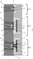
- FIG. 1 shows a device with amorphous semiconductor regions, amongst other features, and respective fabrication processes in accordance with aspects of the present disclosure.
- the device 10 of FIG. 1 includes a semiconductor substrate 12 preferably composed of single crystalline Si material with any suitable crystallographic orientation (e.g., a (100), (110), (111), or (001) crystallographic orientation).
- the semiconductor substrate 12 may be composed of other bulk semiconductor materials, including but not limited to, SiGe, SiGeC, SiC, GaAs, InAs, InP, and other III/V or II/VI compound semiconductors.
- device region 100 is representative of a SiGe HBT.
- FIG. 1 further shows a sub-collector region 16 formed in the semiconductor substrate 12 within the HBT region 100.
- the sub-collector region 16 may be formed by an implantation process, e.g., using an N-type implant for a HBT NPN device as described with respect to FIG. 5A .
- the sub-collector region 16 could diffuse into the semiconductor substrate 12 about 0.1-1.0 micron deep in a 2 micron thick substrate material 12; although other dimensions are contemplated herein.
- the sub-collector region 16 may extend between deep trench isolation structures 18.
- the deep trench isolation structures 18 may be used to define the collector region 20 in the device region 100, above the sub-collector region 16. More specifically, the deep trench isolation structures 18 may be used to encapsulate an HBT device 32 to provide isolation of the HBT device 32, e.g., isolating or surrounding a collector region 20.
- the collector region 20 may be an epitaxial semiconductor material, e.g., Si, grown over the sub-collector region 16.
- Shallow trench isolation structures 22 may be formed in the collector region 20, over the sub-collector region 16 in the HBT region 100. As shown, the sub-collector region 16 can be vertically below and does not contact the shallow trench isolation structures 22. In alternative embodiments, it is possible to have the shallow trench isolation structures 22 touching the sub-collector region 16.
- the deep trench isolation structures 18 and shallow trench isolation structures 22 can be formed by conventional lithography, etching and deposition methods known to those of skill in the art as described in more detail with respect to FIG. 5C .
- non-single-crystal semiconductor regions 24 may be formed at an impact ionization peak point, e.g., close to a collector base junction.
- the non-single-crystal semiconductor regions 24 may be trap rich regions and, more specifically, non-single-crystal semiconductor regions 24 formed close to the collector base junction and at a corner of the shallow trench isolation structures 22.
- the non-single-crystal semiconductor regions 24 may be formed in the collector region 20, above the sub-collector region 16.
- the non-single-crystal semiconductor regions 24 may be in direct contact at a corner and, more preferably a sidewall and bottom surface of the shallow trench isolation structures 22, extending to and contacting an upper surface of the sub-collector region 16. As described with respect to FIGS. 2 and 3 , the non-single-crystal semiconductor regions 24 may be either below or along an inner sidewall of the shallow trench isolation structures 22. In further embodiments, the non-single-crystal semiconductor regions 24 may or may not contact the sub-collector region 16.
- the non-single-crystal semiconductor regions 24 may be an amorphous layer of silicon material.
- the non-single-crystal semiconductor regions 24 may be a high resistivity amorphous semiconductor material located at least at a corner of the shallow trench isolation structures 22 in the collector region 20.
- the non-single-crystal semiconductor regions 24 may be trap rich regions comprising damaged silicon material, e.g., a-Si and/or polysilicon material abutting the shallow trench isolation structures 22.
- the non-single-crystal semiconductor regions 24 can be formed using an implantation mask to define selected areas exposed for the implantation of the non-single-crystal semiconductor regions 24, as described in further detail with respect to FIG. 5E .
- the bipolar heterojunction transistor 32 includes a base region 38 and an emitter region 40.
- the base region 38 can be composed of doped SiGe material as an example.
- the dopant of the SiGe material can be a p-type dopant, e.g., Boron (B).
- the emitter region 40 may be doped Si material, as an example.
- the dopant can be a n-type dopant, e.g., Arsenic (As), Phosphorus (P) and Sb, among other suitable examples.
- the base region 38 and the emitter region 40 may be formed, e.g., deposited, by conventional CVD processes, followed by conventional lithography and etching (e.g., patterning) processes.
- the base region 38 may be provided above the collector region 20 and in contact with the semiconductor substrate 12.
- Sidewalls 42 may be formed on the emitter region 40, e.g., oxide and/or nitride material, as is known in the art.
- the non-single-crystal semiconductor regions 24 preferably do not contact the base region 38; instead, the non-single-crystal semiconductor regions 24 are close to the collector side of the junction of the collector region 20 and the base region 38.
- a silicide process can be provided to form contacts to the appropriate active regions, e.g., base region 38, emitter region 40 and collector region 20.
- the silicide process begins with deposition of a thin transition metal layer, e.g., nickel, cobalt or titanium, over fully formed and patterned devices. After deposition of the material, the structure can be heated allowing the transition metal to react with exposed silicon (or other semiconductor material as described herein) in the active regions of the semiconductor device (e.g., base region 38, emitter region 40 and collector region 20) forming a low-resistance transition metal silicide. Following the reaction, any remaining transition metal can be removed by chemical etching, leaving silicide contacts in the active regions of the device.
- a thin transition metal layer e.g., nickel, cobalt or titanium
- An interlevel dielectric material 44 may be formed (e.g., deposited) in the device region 100 with contacts 46 formed to the silicide contacts of the e.g., base region 38, emitter region 40 and collector region 20 (e.g., contacting reach through implants).
- the interlevel dielectric material 44 may be an oxide and/or nitride material deposited by a CVD process.
- the contacts 46 can be metal or metal alloy material, preferably composed of tungsten.
- the contacts 46 can be formed by conventional lithography and etching processes through the interlevel dielectric material 44 to form trenches, followed by deposition of conductive material within the trenches. Any residual material on the interlevel dielectric material 44 can be removed by a CMP process.
- FIG. 2 shows a structure 10a comprising the device 32 with non-single-crystal semiconductor regions 24a.
- the non-single-crystal semiconductor regions 24a contact an inner sidewall of the shallow trench isolation structures 22, extending to and contacting an upper surface of the sub-collector region 16.
- the non-single-crystal semiconductor regions 24a may be within the collector region 20 and may or may not contact the sub-collector region 16.
- the non-single-crystal semiconductor regions 24a may be a high resistivity material such as damaged silicon material, e.g., a-Si and/or polysilicon material touching the inner sidewalls of the shallow trench isolation structures 22 (at a corner thereof).
- the remaining features of the structure 10b are similar to the structure 10 of FIG. 1 .
- FIG. 3 shows a structure 10b comprising the device 32 with the non-single-crystal semiconductor regions 24b in contact with a bottom surface of the shallow trench isolation structures 22, extending to and contacting an upper surface of the sub-collector region 16.
- the non-single-crystal semiconductor regions 24b may be within the collector region 20 and may or may not contact the sub-collector region 16.
- the non-single-crystal semiconductor regions 24b may be a high resistivity material such as damaged silicon material, e.g., trap rich regions, a-Si and/or polysilicon material touching the inner sidewalls of the shallow trench isolation structures 22.
- the remaining features of the structure 10c are similar to the structures 10, 10a of FIGS. 1 and 2 .
- FIG. 4 shows integrated devices in accordance with aspects of the present disclosure.
- the integrated device include device regions 100, 200, 300 formed on a same wafer, e.g., semiconductor substrate 12.
- the device region 100 is representative of an HBT 32 with the non-single-crystal semiconductor regions 24 as described with respect to FIGS. 1-3 .
- the device region 200 may be representative of an HBT 32a without amorphous semiconductor regions, and device region 300 may be representative of a field effect transistor (FET) 32b.
- FET field effect transistor
- the HBTs 32, 32a can be a SiGe power amplifier, as an example.
- the HBT 32a may include a doped collector region 20a which exhibits high Ft/Fmax.
- the FET 32b can be a switch or LNA or a logic transistor.
- the FET 32b includes source and drain regions 50 and a gate electrode 52, each of which electrically connect to the contacts 46.
- the gate electrode 52 may be formed on a gate dielectric material also representatively shown as reference numeral 52.
- the gate electrode 52 may be a workfunction metal as is known in the art, and the gate dielectric material may be a high-k dielectric material as an example.
- the field effect transistor 32b may also be devoid of the amorphous semiconductor regions.
- the FET 32b can be formed using conventional gate formation processes, e.g., gate first processes or replacement gate processes.
- gate first processes a gate dielectric material and workfunction material(s) are deposited and patterned using conventional CMOS fabrication process as is known in the art.
- the gate dielectric material can be a high-k gate dielectric material, e.g., HfO 2 .
- the workfunction materials include, e.g., Ti, TiAlC, Al, TiAl, TaN, TaAlC, TiN, TiC, TaC, Co, etc.
- the workfunction materials may be deposited by chemical vapor deposition (CVD), physical vapor deposition (PVD) including sputtering, atomic layer deposition (ALD) or other suitable method.
- a sidewall material e.g. oxide and/or nitride, can be formed on the patterned gate dielectric material and workfunction material(s) using conventional deposition processes followed by an anisotropic etching process.
- the source and drain regions 50 can be formed by conventional ion implantation processes, as an example. In alternative examples, the source and drain regions 50 can be raised source and drain regions formed by a doped epitaxial process.
- FIGS. 5A-5E show fabrication processes for manufacturing the device shown in FIG. 1 . Similar processes may be used to manufacture the device of FIGS. 2 and 3 .
- the sub-collector region 16 may be formed in the semiconductor substrate 12 by an ion implant process, using a patterned mask 50a.
- the patterned implantation mask 50a can be used to define selected areas exposed for the implantation of the sub-collector region 16.
- the patterned implantation mask 50a may include a layer of a light-sensitive material, such as an organic photoresist, applied by a spin coating process, pre-baked, exposed to light projected through a photomask, baked after exposure, and developed with a chemical developer.
- the patterned implantation mask 50a has a thickness and stopping power sufficient to block masked areas against receiving a dose of the implanted ions.
- the patterned implantation mask 50 used to select the exposed area can be stripped after implantation. Following the implant process, an anneal can be performed to repair the damage from the implant.
- the implant can be a n-type dopant, e.g., Arsenic (As), Phosphorus (P) and Sb, among other suitable examples.
- a collector region 20 is formed over the sub-collector region 16.
- the collector region 20 may be formed by an epitaxial growth process as is known in the art.
- the collector region 20 may be Si material, as an example.
- shallow trench isolation structures 22 are formed in the semiconductor substrate 12.
- the shallow trench isolation structures 22 (and deep trench isolation structures (not shown in this representation)) can be formed by conventional lithography, etching and deposition methods known to those of skill in the art.
- a resist formed over the semiconductor substrate 12 is exposed to energy (light) to form a pattern (opening).
- An etching process with a selective chemistry, e.g., reactive ion etching (RIE), can be used to form one or more trenches in the semiconductor substrate 12 through the openings of the resist.
- RIE reactive ion etching
- insulator material e.g., SiO 2
- CVD chemical vapor deposition
- Any residual insulator material on the surface of the semiconductor substrate 12 can be removed, e.g., planarized, by conventional chemical mechanical polishing (CMP) processes. This process will also planarize the shallow trench isolation structures 22.
- CMP chemical mechanical polishing
- reach through implants 20a may be formed to the sub-collector region 16.
- the reach through implants 20a may be formed by an ion implantation process, using the patterned implantation mask 50b in a similar manner as already described herein.
- the non-single-crystal semiconductor regions 24 are formed in the collector region 20, above the sub-collector region 16.
- the non-single-crystal semiconductor regions 24 may be formed by an implantation process, using the patterned implantation mask 50c.
- the non-single-crystal semiconductor regions 24 can be a high resistivity region, e.g., higher than the resistivity of the semiconductor substrate 12, which significantly reduces substrate leakage.
- the non-single-crystal semiconductor regions 24 can be a trap rich regions comprising amorphous material, e.g., polycrystalline silicon layer, with a high resistivity.
- the non-single-crystal semiconductor regions 24 may be formed by a blanket argon implant process; although the use of any non-dopant or noble gas is contemplated herein for the implantation process.
- the semiconductor substrate 12 can be subjected to an argon implant at 400 KeV and a dose of 1.25 ⁇ 10 15 cm -2 .
- other implant parameters are contemplated herein depending on the desired thickness and depth of the implant region including, e.g., the ion dose may be less than or greater than 1.25 ⁇ 10 15 cm -2 or within a range of 1 ⁇ 10 13 cm -2 to 5 ⁇ 10 16 cm -2 .
- the thickness of the non-single-crystal semiconductor regions 24 can be adjusted depending on the parameters of the implantation process.
- an anneal process may be performed that recrystallizes the top layer of the non-single-crystal semiconductor regions 24 into a single crystal region.
- the thermal process repairs or heals the damage to (i.e., recrystallize or regrow) the semiconductor material of the modified layer.
- the anneal may be a rapid thermal anneal (RTA) performed with a peak temperature in a range of 860°C to 1125°C with a dwell time at the peak temperature of 34 milliseconds to 60 seconds and, in a particular, the peak temperature may be 1000°C held for a dwell time of 5 seconds. In this way, the non-single-crystal semiconductor regions 24 will not contact the base region 38 as shown in FIGS. 1-4 .
- RTA rapid thermal anneal
- SoC system on chip
- SoC is an integrated circuit (also known as a "chip") that integrates all components of an electronic system on a single chip or substrate. As the components are integrated on a single substrate, SoCs consume much less power and take up much less area than multi-chip designs with equivalent functionality. Because of this, SoCs are becoming the dominant force in the mobile computing (such as in Smartphones) and edge computing markets. SoC is also commonly used in embedded systems and the Internet of Things.
- the method(s) as described above is used in the fabrication of integrated circuit chips.
- the resulting integrated circuit chips can be distributed by the fabricator in raw wafer form (that is, as a single wafer that has multiple unpackaged chips), as a bare die, or in a packaged form.
- the chip is mounted in a single chip package (such as a plastic carrier, with leads that are affixed to a motherboard or other higher level carrier) or in a multichip package (such as a ceramic carrier that has either or both surface interconnections or buried interconnections).
- the chip is then integrated with other chips, discrete circuit elements, and/or other signal processing devices as part of either (a) an intermediate product, such as a motherboard, or (b) an end product.
- the end product can be any product that includes integrated circuit chips, ranging from toys and other low-end applications to advanced computer products having a display, a keyboard or other input device, and a central processor.
Landscapes
- Bipolar Transistors (AREA)
Abstract
Description
- The present disclosure relates to semiconductor structures and, more particularly, to heterojunction bipolar transistors (HBTs) with amorphous semiconductor regions and methods of manufacture.
- A heterojunction bipolar transistor (HBT) is a type of bipolar junction transistor (BJT) which uses differing semiconductor materials for the emitter and base regions or collector and base regions, creating a heterojunction. Si/SiGe HBTs are used in power amplifier applications due to good RF performance, high breakdown voltage and integration with CMOS devices.
- In HBT applications, though, there is a trade-off between breakdown voltage and high RF performance. That is, an increase in the breakdown voltage of a HBT may result in degrading RF device performance. In an attempt to increase breakdown voltage without degrading device performance, designs have included adjusting the dopant profile of the collector/base junction, using different substrate materials which exhibit wider bandgaps, or using an insulator gate bipolar transistor. These schemes, though, result in poor RF performance.
- In an aspect of the disclosure, a structure comprises: a heterojunction bipolar transistor comprising a collector region, a base region and an emitter region; and at least one non-single-crystal semiconductor region in the collector region of the heterojunction bipolar transistor.
- Additional features of the structure are set forth in dependent claims 2 to 9.
- In an aspect of the disclosure, a structure comprises: a heterojunction bipolar transistor comprising a collector region, a base region and an emitter region; a shallow trench isolation structure below the base region in a semiconductor substrate of the collector region; and at least one amorphous semiconductor region close to a junction of the base region and the collector region and a corner of the shallow trench isolation structure.
- Additional features of the structure are set forth in dependent claims 11 to 14.
- In an aspect of the disclosure, a method comprises: forming a heterojunction bipolar transistor comprising a collector region, a base region and an emitter region; and forming at least one amorphous semiconductor region in the collector region of the heterojunction bipolar transistor.
- The present disclosure is described in the detailed description which follows, in reference to the noted plurality of drawings by way of non-limiting examples of exemplary embodiments of the present disclosure.
-
FIG. 1 shows a device with amorphous semiconductor regions, amongst other features, and respective fabrication processes in accordance with aspects of the present disclosure. -
FIG. 2 shows a device with amorphous semiconductor regions, amongst other features, in accordance with additional aspects of the present disclosure. -
FIG. 3 shows a device with amorphous semiconductor regions, amongst other features, in accordance with additional aspects of the present disclosure. -
FIG. 4 shows integrated devices on a single wafer and respective fabrication processes in accordance with aspects of the present disclosure. -
FIGS. 5A-5E show fabrication processes for manufacturing the device shown inFIG. 1 . - The present disclosure relates to semiconductor structures and, more particularly, to heterojunction bipolar transistors (HBTs) with amorphous semiconductor regions and methods of manufacture. More specifically, the present disclosure relates to a SiGe heterojunction bipolar transistor (HBT) with a buried amorphous semiconductor region in the collector region. In embodiments, the amorphous semiconductor region comprises a high resistivity semiconductor material adjacent to shallow trench isolation structures and above a sub-collector region. Advantageously, the amorphous semiconductor region increases breakdown voltage of a high voltage (HV) SiGe HBT (e.g., NPN) device, without any significant changes to other performance parameters, e.g., Ccb, Ft, Fmax, Gm etc.
- In embodiments, the SiGe HBT is provided on a bulk wafer with the buried amorphous semiconductor region partially surrounding shallow trench isolation structures above a sub-collector region. In embodiments, the amorphous semiconductor region may be a buried trap rich semiconductor region comprising amorphous Si material (e.g., trap rich polycrystalline silicon material) located below the shallow trench isolation structures and, in embodiments, extending to and contacting the sub-collector region. In further embodiments, the amorphous semiconductor region may be formed close to a collector base junction and at a corner of the shallow trench isolation structures.
- The structures of the present disclosure can be manufactured in a number of ways using a number of different tools. In general, though, the methodologies and tools are used to form structures with dimensions in the micrometer and nanometer scale. The methodologies, i.e., technologies, employed to manufacture the structures of the present disclosure have been adopted from integrated circuit (IC) technology. For example, the structures are built on wafers and are realized in films of material patterned by photolithographic processes on the top of a wafer. In particular, the fabrication of the structures uses three basic building blocks: (i) deposition of thin films of material on a substrate, (ii) applying a patterned mask on top of the films by photolithographic imaging, and (iii) etching the films selectively to the mask.
-
FIG. 1 shows a device with amorphous semiconductor regions, amongst other features, and respective fabrication processes in accordance with aspects of the present disclosure. More specifically, thedevice 10 ofFIG. 1 includes asemiconductor substrate 12 preferably composed of single crystalline Si material with any suitable crystallographic orientation (e.g., a (100), (110), (111), or (001) crystallographic orientation). Thesemiconductor substrate 12 may be composed of other bulk semiconductor materials, including but not limited to, SiGe, SiGeC, SiC, GaAs, InAs, InP, and other III/V or II/VI compound semiconductors. For purposes of this description,device region 100 is representative of a SiGe HBT. -
FIG. 1 further shows asub-collector region 16 formed in thesemiconductor substrate 12 within theHBT region 100. In embodiments, thesub-collector region 16 may be formed by an implantation process, e.g., using an N-type implant for a HBT NPN device as described with respect toFIG. 5A . Depending on the parameters of the implantation process, thesub-collector region 16 could diffuse into thesemiconductor substrate 12 about 0.1-1.0 micron deep in a 2 micronthick substrate material 12; although other dimensions are contemplated herein. - The
sub-collector region 16 may extend between deeptrench isolation structures 18. The deeptrench isolation structures 18 may be used to define thecollector region 20 in thedevice region 100, above thesub-collector region 16. More specifically, the deeptrench isolation structures 18 may be used to encapsulate anHBT device 32 to provide isolation of theHBT device 32, e.g., isolating or surrounding acollector region 20. In embodiments, thecollector region 20 may be an epitaxial semiconductor material, e.g., Si, grown over thesub-collector region 16. - Shallow
trench isolation structures 22 may be formed in thecollector region 20, over thesub-collector region 16 in the HBTregion 100. As shown, thesub-collector region 16 can be vertically below and does not contact the shallowtrench isolation structures 22. In alternative embodiments, it is possible to have the shallowtrench isolation structures 22 touching thesub-collector region 16. The deeptrench isolation structures 18 and shallowtrench isolation structures 22 can be formed by conventional lithography, etching and deposition methods known to those of skill in the art as described in more detail with respect toFIG. 5C . - Still referring to
FIG. 1 , non-single-crystal semiconductor regions 24 may be formed at an impact ionization peak point, e.g., close to a collector base junction. In more specific embodiments, the non-single-crystal semiconductor regions 24 may be trap rich regions and, more specifically, non-single-crystal semiconductor regions 24 formed close to the collector base junction and at a corner of the shallowtrench isolation structures 22. In still more specific embodiments, the non-single-crystal semiconductor regions 24 may be formed in thecollector region 20, above thesub-collector region 16. In these configurations, the non-single-crystal semiconductor regions 24 may be in direct contact at a corner and, more preferably a sidewall and bottom surface of the shallowtrench isolation structures 22, extending to and contacting an upper surface of thesub-collector region 16. As described with respect toFIGS. 2 and3 , the non-single-crystal semiconductor regions 24 may be either below or along an inner sidewall of the shallowtrench isolation structures 22. In further embodiments, the non-single-crystal semiconductor regions 24 may or may not contact thesub-collector region 16. - The non-single-
crystal semiconductor regions 24 may be an amorphous layer of silicon material. In more specific embodiments, the non-single-crystal semiconductor regions 24 may be a high resistivity amorphous semiconductor material located at least at a corner of the shallowtrench isolation structures 22 in thecollector region 20. In further specific embodiments, the non-single-crystal semiconductor regions 24 may be trap rich regions comprising damaged silicon material, e.g., a-Si and/or polysilicon material abutting the shallowtrench isolation structures 22. The non-single-crystal semiconductor regions 24 can be formed using an implantation mask to define selected areas exposed for the implantation of the non-single-crystal semiconductor regions 24, as described in further detail with respect toFIG. 5E . - In the
HBT region 100, thebipolar heterojunction transistor 32 includes abase region 38 and anemitter region 40. Thebase region 38 can be composed of doped SiGe material as an example. In embodiments, the dopant of the SiGe material can be a p-type dopant, e.g., Boron (B). Theemitter region 40 may be doped Si material, as an example. In embodiments, the dopant can be a n-type dopant, e.g., Arsenic (As), Phosphorus (P) and Sb, among other suitable examples. - The
base region 38 and theemitter region 40 may be formed, e.g., deposited, by conventional CVD processes, followed by conventional lithography and etching (e.g., patterning) processes. Thebase region 38 may be provided above thecollector region 20 and in contact with thesemiconductor substrate 12.Sidewalls 42 may be formed on theemitter region 40, e.g., oxide and/or nitride material, as is known in the art. The non-single-crystal semiconductor regions 24 preferably do not contact thebase region 38; instead, the non-single-crystal semiconductor regions 24 are close to the collector side of the junction of thecollector region 20 and thebase region 38. - Following the formation of the device (e.g., HBT 32) in
region 100, a silicide process can be provided to form contacts to the appropriate active regions, e.g.,base region 38,emitter region 40 andcollector region 20. As should be understood by those of skill in the art, the silicide process begins with deposition of a thin transition metal layer, e.g., nickel, cobalt or titanium, over fully formed and patterned devices. After deposition of the material, the structure can be heated allowing the transition metal to react with exposed silicon (or other semiconductor material as described herein) in the active regions of the semiconductor device (e.g.,base region 38,emitter region 40 and collector region 20) forming a low-resistance transition metal silicide. Following the reaction, any remaining transition metal can be removed by chemical etching, leaving silicide contacts in the active regions of the device. - An interlevel
dielectric material 44 may be formed (e.g., deposited) in thedevice region 100 withcontacts 46 formed to the silicide contacts of the e.g.,base region 38,emitter region 40 and collector region 20 (e.g., contacting reach through implants). The interleveldielectric material 44 may be an oxide and/or nitride material deposited by a CVD process. Thecontacts 46 can be metal or metal alloy material, preferably composed of tungsten. Thecontacts 46 can be formed by conventional lithography and etching processes through the interleveldielectric material 44 to form trenches, followed by deposition of conductive material within the trenches. Any residual material on the interleveldielectric material 44 can be removed by a CMP process. -
FIG. 2 shows astructure 10a comprising thedevice 32 with non-single-crystal semiconductor regions 24a. InFIG. 2 , the non-single-crystal semiconductor regions 24a contact an inner sidewall of the shallowtrench isolation structures 22, extending to and contacting an upper surface of thesub-collector region 16. The non-single-crystal semiconductor regions 24a may be within thecollector region 20 and may or may not contact thesub-collector region 16. The non-single-crystal semiconductor regions 24a may be a high resistivity material such as damaged silicon material, e.g., a-Si and/or polysilicon material touching the inner sidewalls of the shallow trench isolation structures 22 (at a corner thereof). The remaining features of thestructure 10b are similar to thestructure 10 ofFIG. 1 . -
FIG. 3 shows astructure 10b comprising thedevice 32 with the non-single-crystal semiconductor regions 24b in contact with a bottom surface of the shallowtrench isolation structures 22, extending to and contacting an upper surface of thesub-collector region 16. The non-single-crystal semiconductor regions 24b may be within thecollector region 20 and may or may not contact thesub-collector region 16. The non-single-crystal semiconductor regions 24b may be a high resistivity material such as damaged silicon material, e.g., trap rich regions, a-Si and/or polysilicon material touching the inner sidewalls of the shallowtrench isolation structures 22. The remaining features of thestructure 10c are similar to thestructures FIGS. 1 and2 . -
FIG. 4 shows integrated devices in accordance with aspects of the present disclosure. The integrated device includedevice regions semiconductor substrate 12. Thedevice region 100 is representative of anHBT 32 with the non-single-crystal semiconductor regions 24 as described with respect toFIGS. 1-3 . Thedevice region 200 may be representative of anHBT 32a without amorphous semiconductor regions, anddevice region 300 may be representative of a field effect transistor (FET) 32b. TheHBTs HBT 32a may include adoped collector region 20a which exhibits high Ft/Fmax. TheFET 32b can be a switch or LNA or a logic transistor. - Still referring to
FIG. 4 , theFET 32b includes source and drainregions 50 and agate electrode 52, each of which electrically connect to thecontacts 46. Thegate electrode 52 may be formed on a gate dielectric material also representatively shown asreference numeral 52. Thegate electrode 52 may be a workfunction metal as is known in the art, and the gate dielectric material may be a high-k dielectric material as an example. Thefield effect transistor 32b may also be devoid of the amorphous semiconductor regions. - The
FET 32b can be formed using conventional gate formation processes, e.g., gate first processes or replacement gate processes. For example, in the gate first processes, a gate dielectric material and workfunction material(s) are deposited and patterned using conventional CMOS fabrication process as is known in the art. The gate dielectric material can be a high-k gate dielectric material, e.g., HfO2. Examples of the workfunction materials include, e.g., Ti, TiAlC, Al, TiAl, TaN, TaAlC, TiN, TiC, TaC, Co, etc. The workfunction materials may be deposited by chemical vapor deposition (CVD), physical vapor deposition (PVD) including sputtering, atomic layer deposition (ALD) or other suitable method. A sidewall material, e.g. oxide and/or nitride, can be formed on the patterned gate dielectric material and workfunction material(s) using conventional deposition processes followed by an anisotropic etching process. The source and drainregions 50 can be formed by conventional ion implantation processes, as an example. In alternative examples, the source and drainregions 50 can be raised source and drain regions formed by a doped epitaxial process. -
FIGS. 5A-5E show fabrication processes for manufacturing the device shown inFIG. 1 . Similar processes may be used to manufacture the device ofFIGS. 2 and3 . - In
FIG. 5A , thesub-collector region 16 may be formed in thesemiconductor substrate 12 by an ion implant process, using a patternedmask 50a. In the implantation process, the patternedimplantation mask 50a can be used to define selected areas exposed for the implantation of thesub-collector region 16. The patternedimplantation mask 50a may include a layer of a light-sensitive material, such as an organic photoresist, applied by a spin coating process, pre-baked, exposed to light projected through a photomask, baked after exposure, and developed with a chemical developer. The patternedimplantation mask 50a has a thickness and stopping power sufficient to block masked areas against receiving a dose of the implanted ions. The patternedimplantation mask 50 used to select the exposed area can be stripped after implantation. Following the implant process, an anneal can be performed to repair the damage from the implant. The implant can be a n-type dopant, e.g., Arsenic (As), Phosphorus (P) and Sb, among other suitable examples. - In
FIG. 5B , acollector region 20 is formed over thesub-collector region 16. In embodiments, thecollector region 20 may be formed by an epitaxial growth process as is known in the art. Thecollector region 20 may be Si material, as an example. - In
FIG. 5C , shallowtrench isolation structures 22 are formed in thesemiconductor substrate 12. The shallow trench isolation structures 22 (and deep trench isolation structures (not shown in this representation)) can be formed by conventional lithography, etching and deposition methods known to those of skill in the art. For example, a resist formed over thesemiconductor substrate 12 is exposed to energy (light) to form a pattern (opening). An etching process with a selective chemistry, e.g., reactive ion etching (RIE), can be used to form one or more trenches in thesemiconductor substrate 12 through the openings of the resist. Following resist removal by a conventional oxygen ashing process or other known stripants, insulator material, e.g., SiO2, can be deposited by any conventional deposition processes, e.g., chemical vapor deposition (CVD). Any residual insulator material on the surface of thesemiconductor substrate 12 can be removed, e.g., planarized, by conventional chemical mechanical polishing (CMP) processes. This process will also planarize the shallowtrench isolation structures 22. - In
FIG. 5D , reach throughimplants 20a may be formed to thesub-collector region 16. The reach throughimplants 20a may be formed by an ion implantation process, using the patternedimplantation mask 50b in a similar manner as already described herein. - In
FIG. 5E , the non-single-crystal semiconductor regions 24 are formed in thecollector region 20, above thesub-collector region 16. The non-single-crystal semiconductor regions 24 may be formed by an implantation process, using the patterned implantation mask 50c.The non-single-crystal semiconductor regions 24 can be a high resistivity region, e.g., higher than the resistivity of thesemiconductor substrate 12, which significantly reduces substrate leakage. For example, the non-single-crystal semiconductor regions 24 can be a trap rich regions comprising amorphous material, e.g., polycrystalline silicon layer, with a high resistivity. In embodiments, the non-single-crystal semiconductor regions 24 may be formed by a blanket argon implant process; although the use of any non-dopant or noble gas is contemplated herein for the implantation process. As an illustrative, non-limiting example, thesemiconductor substrate 12 can be subjected to an argon implant at 400 KeV and a dose of 1.25×1015 cm-2. By way of further illustrative examples, other implant parameters are contemplated herein depending on the desired thickness and depth of the implant region including, e.g., the ion dose may be less than or greater than 1.25×1015 cm-2 or within a range of 1×1013 cm-2 to 5×1016 cm-2. The thickness of the non-single-crystal semiconductor regions 24 can be adjusted depending on the parameters of the implantation process. - Following the implantation process, an anneal process may be performed that recrystallizes the top layer of the non-single-
crystal semiconductor regions 24 into a single crystal region. In particular, the thermal process repairs or heals the damage to (i.e., recrystallize or regrow) the semiconductor material of the modified layer. For example, the anneal may be a rapid thermal anneal (RTA) performed with a peak temperature in a range of 860°C to 1125°C with a dwell time at the peak temperature of 34 milliseconds to 60 seconds and, in a particular, the peak temperature may be 1000°C held for a dwell time of 5 seconds. In this way, the non-single-crystal semiconductor regions 24 will not contact thebase region 38 as shown inFIGS. 1-4 . - The heterojunction bipolar transistor (and other devices disclosed herein) can be utilized in system on chip (SoC) technology. It should be understood by those of skill in the art that SoC is an integrated circuit (also known as a "chip") that integrates all components of an electronic system on a single chip or substrate. As the components are integrated on a single substrate, SoCs consume much less power and take up much less area than multi-chip designs with equivalent functionality. Because of this, SoCs are becoming the dominant force in the mobile computing (such as in Smartphones) and edge computing markets. SoC is also commonly used in embedded systems and the Internet of Things.
- The method(s) as described above is used in the fabrication of integrated circuit chips. The resulting integrated circuit chips can be distributed by the fabricator in raw wafer form (that is, as a single wafer that has multiple unpackaged chips), as a bare die, or in a packaged form. In the latter case the chip is mounted in a single chip package (such as a plastic carrier, with leads that are affixed to a motherboard or other higher level carrier) or in a multichip package (such as a ceramic carrier that has either or both surface interconnections or buried interconnections). In any case the chip is then integrated with other chips, discrete circuit elements, and/or other signal processing devices as part of either (a) an intermediate product, such as a motherboard, or (b) an end product. The end product can be any product that includes integrated circuit chips, ranging from toys and other low-end applications to advanced computer products having a display, a keyboard or other input device, and a central processor.
- The descriptions of the various embodiments of the present disclosure have been presented for purposes of illustration, but are not intended to be exhaustive or limited to the embodiments disclosed. Many modifications and variations will be apparent to those of ordinary skill in the art without departing from the scope and spirit of the described embodiments. The terminology used herein was chosen to best explain the principles of the embodiments, the practical application or technical improvement over technologies found in the marketplace, or to enable others of ordinary skill in the art to understand the embodiments disclosed herein.
Claims (15)
- A structure comprising:a heterojunction bipolar transistor comprising a collector region, a base region and an emitter region; andat least one non-single-crystal semiconductor region in the collector region of the heterojunction bipolar transistor.
- The structure of claim 1, further comprising a sub-collector region vertically below the collector region, and the at least one non-single-crystal semiconductor region being above the sub-collector region within the collector region.
- The structure of claim 1 or 2, further comprising a shallow trench isolation structure below the base region of the heterojunction bipolar transistor, and the at least one non-single-crystal semiconductor region abutting the shallow trench isolation structure.
- The structure of claim 3, wherein the at least one non-single-crystal semiconductor region contacts a sidewall and bottom of the shallow trench isolation structure, and, optionally, wherein the at least one non-single-crystal semiconductor region contacts a sub-collector region of the heterojunction bipolar transistor.
- The structure of claim 3, wherein the at least one non-single-crystal semiconductor region contacts a sidewall of the shallow trench isolation structure or a bottom of the shallow trench isolation structure.
- The structure of one of claims 1 to 5, wherein the at least one non-single-crystal semiconductor region is close to a base collector junction and at a corner of a shallow trench isolation structure within the collector region.
- The structure of claim 6, wherein the non-single-crystal semiconductor region is vertically above a sub-collector region of the heterojunction bipolar transistor and within the collector region.
- The structure of one of claims 1 to 7, wherein the at least one non-single-crystal semiconductor region comprises a trap rich semiconductor material, or wherein the at least non-single-crystal semiconductor region comprises amorphous Si, or wherein the at least one non-single-crystal semiconductor region comprises a polysilicon material.
- The structure of one of claims 1 to 8, further comprising at least one other transistor on a same substrate as the heterojunction bipolar transistor and being devoid of the at least one amorphous semiconductor region.
- A structure comprising:a heterojunction bipolar transistor comprising a collector region, a base region and an emitter region;a shallow trench isolation structure below the base region in a semiconductor substrate of the collector region; andat least one amorphous semiconductor region close to a junction of the base region and the collector region and a corner of the shallow trench isolation structure.
- The structure of claim 10, wherein the heterojunction bipolar transistor comprises a sub-collector region vertically below the collector region, and the at least one amorphous semiconductor region being above the sub-collector region within the collector region.
- The structure of claim 10 or claim 11, wherein the at least one amorphous semiconductor region contacts a sidewall and bottom of the shallow trench isolation structure, or wherein the at least one amorphous semiconductor region contacts one of a sidewall and a bottom of the shallow trench isolation structure.
- The structure of one of claims 10 to 12, wherein the at least one amorphous semiconductor region is close to a base collector junction and at a corner of the shallow trench isolation structure within the collector region.
- The structure of one of claims 10 to 13, wherein the at least one amorphous semiconductor region comprises a polysilicon material.
- A method comprising:forming a heterojunction bipolar transistor comprising a collector region, a base region and an emitter region; andforming at least one amorphous semiconductor region in the collector region of the heterojunction bipolar transistor.
Applications Claiming Priority (1)
| Application Number | Priority Date | Filing Date | Title |
|---|---|---|---|
| US17/978,633 US12237407B2 (en) | 2022-11-01 | 2022-11-01 | Heterojunction bipolar transistor with amorphous semiconductor regions |
Publications (1)
| Publication Number | Publication Date |
|---|---|
| EP4365956A1 true EP4365956A1 (en) | 2024-05-08 |
Family
ID=88017813
Family Applications (1)
| Application Number | Title | Priority Date | Filing Date |
|---|---|---|---|
| EP23196430.5A Pending EP4365956A1 (en) | 2022-11-01 | 2023-09-11 | Heterojunction bipolar transistor with amorphous semiconductor regions |
Country Status (3)
| Country | Link |
|---|---|
| US (1) | US12237407B2 (en) |
| EP (1) | EP4365956A1 (en) |
| CN (1) | CN117995894A (en) |
Citations (3)
| Publication number | Priority date | Publication date | Assignee | Title |
|---|---|---|---|---|
| US20080054406A1 (en) * | 2006-08-31 | 2008-03-06 | Agere Systems Inc. | Method to Improve Performance of a Bipolar Device Using an Amorphizing Implant |
| US20090179303A1 (en) * | 2004-12-11 | 2009-07-16 | Bernd Heinemann | Vertical Bipolar Transistor |
| US20150108549A1 (en) * | 2013-10-22 | 2015-04-23 | International Business Machines Corporation | Formation of a high aspect ratio trench in a semiconductor substrate and a bipolar semiconductor device having a high aspect ratio trench isolation region |
Family Cites Families (34)
| Publication number | Priority date | Publication date | Assignee | Title |
|---|---|---|---|---|
| WO1993016494A1 (en) | 1992-01-31 | 1993-08-19 | Analog Devices, Inc. | Complementary bipolar polysilicon emitter devices |
| US5508211A (en) | 1994-02-17 | 1996-04-16 | Lsi Logic Corporation | Method of making integrated circuit structure with vertical isolation from single crystal substrate comprising isolation layer formed by implantation and annealing of noble gas atoms in substrate |
| FR2804247B1 (en) * | 2000-01-21 | 2002-04-12 | St Microelectronics Sa | METHOD FOR PRODUCING A BIPOLAR TRANSISTOR WITH SELF-ALIGNED EXTRINSIC BASE |
| US7038242B2 (en) | 2001-02-28 | 2006-05-02 | Agilent Technologies, Inc. | Amorphous semiconductor open base phototransistor array |
| JP2002270815A (en) | 2001-03-14 | 2002-09-20 | Hitachi Ltd | Semiconductor device and drive circuit constituted by the semiconductor device |
| US6767797B2 (en) | 2002-02-01 | 2004-07-27 | Agere Systems Inc. | Method of fabricating complementary self-aligned bipolar transistors |
| US6759731B2 (en) | 2002-06-05 | 2004-07-06 | United Microelectronics Corp. | Bipolar junction transistor and fabricating method |
| SG107645A1 (en) | 2002-09-10 | 2004-12-29 | Sarnoff Corp | Electrostatic discharge protection silicon controlled rectifier (esd-scr) for silicon germanium technologies |
| DE10358047A1 (en) | 2003-12-05 | 2005-06-30 | IHP GmbH - Innovations for High Performance Microelectronics/Institut für innovative Mikroelektronik | Complementary bipolar semiconductor device |
| US7144787B2 (en) | 2005-05-09 | 2006-12-05 | International Business Machines Corporation | Methods to improve the SiGe heterojunction bipolar device performance |
| US7972919B2 (en) | 2005-07-18 | 2011-07-05 | International Business Machines Corporation | Vertical PNP transistor and method of making same |
| US7488662B2 (en) | 2005-12-13 | 2009-02-10 | Chartered Semiconductor Manufacturing, Ltd. | Self-aligned vertical PNP transistor for high performance SiGe CBiCMOS process |
| JP2007200936A (en) * | 2006-01-23 | 2007-08-09 | Nec Corp | THIN FILM TRANSISTOR, ITS MANUFACTURING METHOD, AND LIQUID CRYSTAL DISPLAY DEVICE |
| US8710510B2 (en) | 2006-08-17 | 2014-04-29 | Cree, Inc. | High power insulated gate bipolar transistors |
| DE102006059113A1 (en) | 2006-12-08 | 2008-06-12 | IHP GmbH - Innovations for High Performance Microelectronics/Institut für innovative Mikroelektronik | Complementary bipolar semiconductor device |
| US8815654B2 (en) | 2007-06-14 | 2014-08-26 | International Business Machines Corporation | Vertical current controlled silicon on insulator (SOI) device such as a silicon controlled rectifier and method of forming vertical SOI current controlled devices |
| US8415764B2 (en) | 2009-06-02 | 2013-04-09 | Taiwan Semiconductor Manufacturing Company, Ltd. | High-voltage BJT formed using CMOS HV processes |
| US9312335B2 (en) | 2011-09-23 | 2016-04-12 | Alpha And Omega Semiconductor Incorporated | Lateral PNP bipolar transistor with narrow trench emitter |
| US9761700B2 (en) | 2012-06-28 | 2017-09-12 | Skyworks Solutions, Inc. | Bipolar transistor on high-resistivity substrate |
| US9640528B2 (en) | 2014-04-16 | 2017-05-02 | Newport Fab, Llc | Low-cost complementary BiCMOS integration scheme |
| US9722057B2 (en) | 2015-06-23 | 2017-08-01 | Global Foundries Inc. | Bipolar junction transistors with a buried dielectric region in the active device region |
| US9368608B1 (en) | 2015-06-25 | 2016-06-14 | Globalfoundries Inc. | Heterojunction bipolar transistor with improved performance and breakdown voltage |
| US9721969B2 (en) | 2015-06-30 | 2017-08-01 | Globalfoundries Singapore Pte. Ltd. | Creation of wide band gap material for integration to SOI thereof |
| US10622247B2 (en) | 2016-02-19 | 2020-04-14 | Globalwafers Co., Ltd. | Semiconductor on insulator structure comprising a buried high resistivity layer |
| US10468294B2 (en) | 2016-02-19 | 2019-11-05 | Globalwafers Co., Ltd. | High resistivity silicon-on-insulator substrate comprising a charge trapping layer formed on a substrate with a rough surface |
| US10367083B2 (en) | 2016-03-25 | 2019-07-30 | Globalfoundries Inc. | Compact device structures for a bipolar junction transistor |
| EP3273483B1 (en) | 2016-07-22 | 2023-04-26 | STMicroelectronics (Crolles 2) SAS | Method for manufacturing a pnp bipolar transistor parallel to an npn bipolar transistor, as well as n- and p-channel mos transistors |
| US10276490B2 (en) | 2017-07-20 | 2019-04-30 | Avago Technologies International Sales Pte. Limited | Isolation devices with faraday shields |
| US10622262B2 (en) | 2017-10-06 | 2020-04-14 | Newport Fab Llc | High performance SiGe heterojunction bipolar transistors built on thin film silicon-on-insulator substrates for radio frequency applications |
| US10453919B2 (en) | 2017-11-06 | 2019-10-22 | Stmicroelectronics (Crolles 2) Sas | Heterojunction bipolar transistor with counter-doped collector region and increase collector dependent breakdown voltage |
| US10192779B1 (en) | 2018-03-26 | 2019-01-29 | Globalfoundries Inc. | Bulk substrates with a self-aligned buried polycrystalline layer |
| JP7068211B2 (en) | 2019-02-15 | 2022-05-16 | 株式会社東芝 | Semiconductor device |
| US11171015B2 (en) | 2019-09-11 | 2021-11-09 | Taiwan Semiconductor Manufacturing Company, Ltd. | Multi-layered polysilicon and oxygen-doped polysilicon design for RF SOI trap-rich poly layer |
| US11721719B2 (en) | 2020-10-20 | 2023-08-08 | Globalfoundries U.S. Inc. | Heterojunction bipolar transistor with buried trap rich isolation region |
-
2022
- 2022-11-01 US US17/978,633 patent/US12237407B2/en active Active
-
2023
- 2023-09-11 EP EP23196430.5A patent/EP4365956A1/en active Pending
- 2023-10-25 CN CN202311390844.7A patent/CN117995894A/en active Pending
Patent Citations (3)
| Publication number | Priority date | Publication date | Assignee | Title |
|---|---|---|---|---|
| US20090179303A1 (en) * | 2004-12-11 | 2009-07-16 | Bernd Heinemann | Vertical Bipolar Transistor |
| US20080054406A1 (en) * | 2006-08-31 | 2008-03-06 | Agere Systems Inc. | Method to Improve Performance of a Bipolar Device Using an Amorphizing Implant |
| US20150108549A1 (en) * | 2013-10-22 | 2015-04-23 | International Business Machines Corporation | Formation of a high aspect ratio trench in a semiconductor substrate and a bipolar semiconductor device having a high aspect ratio trench isolation region |
Also Published As
| Publication number | Publication date |
|---|---|
| US12237407B2 (en) | 2025-02-25 |
| CN117995894A (en) | 2024-05-07 |
| US20240145585A1 (en) | 2024-05-02 |
Similar Documents
| Publication | Publication Date | Title |
|---|---|---|
| US12324227B2 (en) | Heterojunction bipolar transistor with buried trap rich isolation region | |
| US12170313B2 (en) | Heterojunction bipolar transistor with buried trap rich isolation region | |
| US12046633B2 (en) | Airgap structures in auto-doped region under one or more transistors | |
| US12349375B2 (en) | Lateral bipolar transistors with gate structure aligned to extrinsic base | |
| US20230197787A1 (en) | Bipolar transistors | |
| EP4340026B1 (en) | Trigger for silicon controlled rectifier | |
| US11145725B2 (en) | Heterojunction bipolar transistor | |
| US6767797B2 (en) | Method of fabricating complementary self-aligned bipolar transistors | |
| US11843034B2 (en) | Lateral bipolar transistor | |
| US20250006824A1 (en) | Transistor with wrap-around extrinsic base | |
| EP4443518A1 (en) | Low capacitance and low resistance devices | |
| EP4525048A1 (en) | Bipolar transistors | |
| EP4369385A1 (en) | Integrated structure with trap rich regions and low resistivity regions | |
| US12237407B2 (en) | Heterojunction bipolar transistor with amorphous semiconductor regions | |
| US20230352570A1 (en) | Bipolar junction transistor | |
| US11855195B2 (en) | Transistor with wrap-around extrinsic base | |
| US11837460B2 (en) | Lateral bipolar transistor |
Legal Events
| Date | Code | Title | Description |
|---|---|---|---|
| PUAI | Public reference made under article 153(3) epc to a published international application that has entered the european phase |
Free format text: ORIGINAL CODE: 0009012 |
|
| STAA | Information on the status of an ep patent application or granted ep patent |
Free format text: STATUS: THE APPLICATION HAS BEEN PUBLISHED |
|
| AK | Designated contracting states |
Kind code of ref document: A1 Designated state(s): AL AT BE BG CH CY CZ DE DK EE ES FI FR GB GR HR HU IE IS IT LI LT LU LV MC ME MK MT NL NO PL PT RO RS SE SI SK SM TR |
|
| STAA | Information on the status of an ep patent application or granted ep patent |
Free format text: STATUS: REQUEST FOR EXAMINATION WAS MADE |
|
| 17P | Request for examination filed |
Effective date: 20240506 |
|
| RBV | Designated contracting states (corrected) |
Designated state(s): AL AT BE BG CH CY CZ DE DK EE ES FI FR GB GR HR HU IE IS IT LI LT LU LV MC ME MK MT NL NO PL PT RO RS SE SI SK SM TR |
|
| STAA | Information on the status of an ep patent application or granted ep patent |
Free format text: STATUS: EXAMINATION IS IN PROGRESS |