EP4365581A1 - Fluidic chip and dielectrophoresis device - Google Patents
Fluidic chip and dielectrophoresis device Download PDFInfo
- Publication number
- EP4365581A1 EP4365581A1 EP22833234.2A EP22833234A EP4365581A1 EP 4365581 A1 EP4365581 A1 EP 4365581A1 EP 22833234 A EP22833234 A EP 22833234A EP 4365581 A1 EP4365581 A1 EP 4365581A1
- Authority
- EP
- European Patent Office
- Prior art keywords
- channel
- electrodes
- main
- inspection
- pair
- Prior art date
- Legal status (The legal status is an assumption and is not a legal conclusion. Google has not performed a legal analysis and makes no representation as to the accuracy of the status listed.)
- Pending
Links
Images



Classifications
-
- C—CHEMISTRY; METALLURGY
- C12—BIOCHEMISTRY; BEER; SPIRITS; WINE; VINEGAR; MICROBIOLOGY; ENZYMOLOGY; MUTATION OR GENETIC ENGINEERING
- C12M—APPARATUS FOR ENZYMOLOGY OR MICROBIOLOGY; APPARATUS FOR CULTURING MICROORGANISMS FOR PRODUCING BIOMASS, FOR GROWING CELLS OR FOR OBTAINING FERMENTATION OR METABOLIC PRODUCTS, i.e. BIOREACTORS OR FERMENTERS
- C12M1/00—Apparatus for enzymology or microbiology
- C12M1/34—Measuring or testing with condition measuring or sensing means, e.g. colony counters
-
- B—PERFORMING OPERATIONS; TRANSPORTING
- B01—PHYSICAL OR CHEMICAL PROCESSES OR APPARATUS IN GENERAL
- B01L—CHEMICAL OR PHYSICAL LABORATORY APPARATUS FOR GENERAL USE
- B01L3/00—Containers or dishes for laboratory use, e.g. laboratory glassware; Droppers
- B01L3/50—Containers for the purpose of retaining a material to be analysed, e.g. test tubes
- B01L3/502—Containers for the purpose of retaining a material to be analysed, e.g. test tubes with fluid transport, e.g. in multi-compartment structures
- B01L3/5027—Containers for the purpose of retaining a material to be analysed, e.g. test tubes with fluid transport, e.g. in multi-compartment structures by integrated microfluidic structures, i.e. dimensions of channels and chambers are such that surface tension forces are important, e.g. lab-on-a-chip
- B01L3/502761—Containers for the purpose of retaining a material to be analysed, e.g. test tubes with fluid transport, e.g. in multi-compartment structures by integrated microfluidic structures, i.e. dimensions of channels and chambers are such that surface tension forces are important, e.g. lab-on-a-chip specially adapted for handling suspended solids or molecules independently from the bulk fluid flow, e.g. for trapping or sorting beads or physically stretching molecules
-
- B—PERFORMING OPERATIONS; TRANSPORTING
- B03—SEPARATION OF SOLID MATERIALS USING LIQUIDS OR USING PNEUMATIC TABLES OR JIGS; MAGNETIC OR ELECTROSTATIC SEPARATION OF SOLID MATERIALS FROM SOLID MATERIALS OR FLUIDS; SEPARATION BY HIGH-VOLTAGE ELECTRIC FIELDS
- B03C—MAGNETIC OR ELECTROSTATIC SEPARATION OF SOLID MATERIALS FROM SOLID MATERIALS OR FLUIDS; SEPARATION BY HIGH-VOLTAGE ELECTRIC FIELDS
- B03C5/00—Separating dispersed particles from liquids by electrostatic effect
- B03C5/005—Dielectrophoresis, i.e. dielectric particles migrating towards the region of highest field strength
-
- B—PERFORMING OPERATIONS; TRANSPORTING
- B03—SEPARATION OF SOLID MATERIALS USING LIQUIDS OR USING PNEUMATIC TABLES OR JIGS; MAGNETIC OR ELECTROSTATIC SEPARATION OF SOLID MATERIALS FROM SOLID MATERIALS OR FLUIDS; SEPARATION BY HIGH-VOLTAGE ELECTRIC FIELDS
- B03C—MAGNETIC OR ELECTROSTATIC SEPARATION OF SOLID MATERIALS FROM SOLID MATERIALS OR FLUIDS; SEPARATION BY HIGH-VOLTAGE ELECTRIC FIELDS
- B03C5/00—Separating dispersed particles from liquids by electrostatic effect
- B03C5/02—Separators
- B03C5/022—Non-uniform field separators
- B03C5/026—Non-uniform field separators using open-gradient differential dielectric separation, i.e. using electrodes of special shapes for non-uniform field creation, e.g. Fluid Integrated Circuit [FIC]
-
- C—CHEMISTRY; METALLURGY
- C12—BIOCHEMISTRY; BEER; SPIRITS; WINE; VINEGAR; MICROBIOLOGY; ENZYMOLOGY; MUTATION OR GENETIC ENGINEERING
- C12M—APPARATUS FOR ENZYMOLOGY OR MICROBIOLOGY; APPARATUS FOR CULTURING MICROORGANISMS FOR PRODUCING BIOMASS, FOR GROWING CELLS OR FOR OBTAINING FERMENTATION OR METABOLIC PRODUCTS, i.e. BIOREACTORS OR FERMENTERS
- C12M1/00—Apparatus for enzymology or microbiology
-
- G—PHYSICS
- G01—MEASURING; TESTING
- G01N—INVESTIGATING OR ANALYSING MATERIALS BY DETERMINING THEIR CHEMICAL OR PHYSICAL PROPERTIES
- G01N27/00—Investigating or analysing materials by the use of electric, electrochemical, or magnetic means
- G01N27/26—Investigating or analysing materials by the use of electric, electrochemical, or magnetic means by investigating electrochemical variables; by using electrolysis or electrophoresis
- G01N27/416—Systems
- G01N27/447—Systems using electrophoresis
-
- B—PERFORMING OPERATIONS; TRANSPORTING
- B03—SEPARATION OF SOLID MATERIALS USING LIQUIDS OR USING PNEUMATIC TABLES OR JIGS; MAGNETIC OR ELECTROSTATIC SEPARATION OF SOLID MATERIALS FROM SOLID MATERIALS OR FLUIDS; SEPARATION BY HIGH-VOLTAGE ELECTRIC FIELDS
- B03C—MAGNETIC OR ELECTROSTATIC SEPARATION OF SOLID MATERIALS FROM SOLID MATERIALS OR FLUIDS; SEPARATION BY HIGH-VOLTAGE ELECTRIC FIELDS
- B03C2201/00—Details of magnetic or electrostatic separation
- B03C2201/26—Details of magnetic or electrostatic separation for use in medical or biological applications
Definitions
- the present invention relates to a channel chip and a dielectrophoresis device.
- Channel chips that use a dielectrophoretic force to separate and collect objects to be collected have been known in the past.
- This type of channel chip includes a channel (microchannel) into which a liquid containing the objects to be collected is injected, and electrodes (microelectrode) for electrically capturing the objects in the liquid.
- a channel chip is disclosed, for example, in Patent Literature 1.
- Patent Literature 1 Japanese Patent Application Laid-Open No. 2017-134020
- Variations can occur in the thickness and relative dielectric constant of an insulating protective film for protecting in-plane electrodes and in the resistivity of electrode metal due to the manufacturing steps of the channel chip. If surface organic contamination occurs in the course of manufacture, organic residue thereof can also affect the dielectrophoretic force. There is a likelihood that these cause a reduction in dielectrophoretic force to such a degree that the objects to be collected cannot be captured or cause an excessive force to such a degree that the objects to be collected are damaged.
- the electrodes For advance evaluation of the performance of the electrodes, it is also contemplated to inspect the electrodes for performance, with the liquid injected into the channel.
- the injection of the liquid into the channel might cause new surface contamination or cause clogging of the channel due to the presence of particles.
- a first aspect is intended for a channel chip comprising: a substrate; a main channel disposed on one main surface of the substrate and capable of receiving a liquid therein; a liquid reservoir disposed on the main surface of the substrate in spaced apart relation to the main channel and capable of receiving a liquid therein; a pair of main electrodes disposed between the main surface of the substrate and the main channel; and at least one pair of inspection electrodes disposed between the main surface of the substrate and the liquid reservoir.
- a second aspect is intended for the channel chip of the first aspect, wherein the liquid reservoir includes an inspection channel capable of passing a liquid therethrough, and wherein the pair of inspection electrodes are disposed between the main surface of the substrate and the inspection channel.
- a third aspect is intended for the channel chip of the first or second aspect, wherein a first overlapping portion of the pair of main electrodes which overlaps the main channel is equal in area to a second overlapping portion of the pair of inspection electrodes which overlaps the liquid reservoir.
- a fourth aspect is intended for the channel chip of any one of the first to third aspects, wherein the at least one pair of inspection electrode includes not less than two pairs of inspection electrodes.
- a fifth aspect is intended for the channel chip of the fourth aspect, wherein the at least one pair of inspection electrodes include three pairs of inspection electrodes.
- a sixth aspect is intended for the channel chip of any one of the first to fifth aspects, wherein the pair of main electrodes and the pair of inspection electrodes are disposed adjacent to each other.
- a seventh aspect is intended for the channel chip of any one of the first to sixth aspects, wherein the pair of main electrodes and the pair of inspection electrodes have respective surfaces covered with an insulating protective film, and wherein the main channel and the liquid reservoir are disposed on the insulating protective film.
- An eighth aspect is intended for the channel chip of any one of the first to seventh aspects, wherein the pair of main electrodes and the pair of inspection electrodes have a comb tooth shape.
- a ninth aspect is intended for a dielectrophoresis device comprising: a channel chip as recited in any one of the first to eighth aspects; and a power supply part for applying a voltage to the pair of main electrodes and the pair of inspection electrodes.
- the pair of main electrodes corresponding to the main channel and the pair of inspection electrodes corresponding to the liquid reservoir are disposed on the same substrate.
- the pair of inspection electrodes are inspected for performance, whereby the performance of the pair of main electrodes is appropriately evaluated without using the main channel and the pair of main electrodes.
- the pair of inspection electrodes overlap the inspection channel of the liquid reservoir, whereby the conditions of the environment in which the pair of inspection electrodes are disposed are brought closer to the conditions of the environment in which the pair of main electrodes are disposed.
- the performance of the pair of main electrodes is appropriately evaluated based on the inspection results of the pair of inspection electrodes.
- the performance of the pair of inspection electrodes is the same as that of the pair of main electrodes because the area of the second overlapping portion of the pair of inspection electrodes is equal to that of the first overlapping portion of the pair of main electrodes.
- the performance of the pair of main electrodes is appropriately evaluated based on the inspection results of the pair of inspection electrodes.
- the performance of the pair of main electrodes is appropriately evaluated by averaging the measurement results of the plurality of pairs of inspection electrodes.
- the provision of the three pairs of inspection electrodes ensures the minimum number of samples required to obtain an average error and suppresses an increase in size of the channel chip.
- the pair of main electrodes and the pair of inspection electrodes are disposed adjacent to each other, so that the conditions of the environment in which the pair of inspection electrodes are disposed are brought closer to the conditions of the environment in which the pair of main electrodes are disposed.
- the performance of the pair of main electrodes is appropriately evaluated based on the inspection results of the pair of inspection electrodes.
- the pair of main electrodes and the pair of inspection electrodes are protected by the insulating protective film.
- the pair of main electrodes and the inspection electrodes are in a shortened and parallel comb tooth shape, whereby the low-resistance and uniform dielectrophoretic force is applied into the liquid.
- Fig. 1 is a plan view showing a dielectrophoresis device 1 according to a first embodiment.
- Fig. 2 is a schematic sectional view of a channel chip 11 taken along a line A-A shown in Fig. 1 .
- the dielectrophoresis device 1 includes the channel chip 11, a plurality of power supply parts 13, and a controller 15.
- the channel chip 11 is a device for electrically separating and collecting objects to be collected that are contained in a liquid of a specimen.
- Conceivable examples of the liquid of the specimen include body fluids such as blood, and physiological saline solution.
- the objects to be collected are substances present in liquids, and conceivable specific examples thereof include microorganisms, cells, proteins, and nucleic acids.
- the power supply parts 13 apply voltage to respective electrodes disposed in the channel chip 11.
- the controller 15 controls the voltage applied by the power supply parts 13.
- the controller 15 is configured with a computer having a general-purpose processor such as a CPU, a RAM, and the like.
- the controller 15 may include a purpose-built circuit (such as an application specific integrated circuit (ASIC)).
- ASIC application specific integrated circuit
- the channel chip 11 includes a substrate 21, a main channel 31, a pair of main electrodes 33a and 33b, a liquid reservoir 40, and a plurality of pairs (in this embodiment, three pairs) of inspection electrodes 43a and 43b.
- the substrate 21 is made of quartz glass, for example. However, the material of the substrate 21 is not limited to quartz glass, and may be selected as appropriate.
- the substrate 21 has a substantially rectangular planar shape. However, the shape of the substrate 21 is not limited to the substantially rectangular planar shape.
- the main channel 31 is capable of receiving therein a liquid containing the objects to be collected.
- the main channel 31 includes a separation channel 311 and a pair of collection channels 313a and 313b.
- the separation channel 311 is an elongated channel extending linearly.
- the separation channel 311 has a first end connected to a first supply part 315.
- the first supply part 315 has a first supply opening 316 for injecting therethrough a liquid to flow into the separation channel 311.
- the main channel 31 branches into the collection channel 313a and the collection channel 313b.
- the collection channel 313a is a channel for collecting the objects to be collected that flow through the separation channel 311.
- the collection channel 313b is a channel for collecting objects not to be collected that flow through the separation channel 311.
- Each of the collection channels 313a and 313b has a first end connected to the second end of the separation channel 311.
- the collection channel 313a has a second end connected to a first collection part 317a.
- the collection channel 313b has a second end connected a first collection part 317b.
- the first collection part 317a has a first collection opening 318 for collecting the liquid flowing through the collection channel 313a.
- the first collection part 317b has a first collection opening 318 for collecting the liquid flowing through the collection channel 313b.
- the main electrodes 33a and 33b are disposed on an upper surface 211 of the substrate 21.
- the main electrodes 33a and 33b have respective upper surfaces covered with an insulating protective film 23.
- the insulating protective film 23 is, for example, an oxide film (such as a silicon oxide film (SiOx)). It should be noted that the insulating protective film 23 may be a nitride film (such as a silicon nitride film).
- the main electrodes 33a and 33b are covered with the insulating protective film 23, which in turn suppresses electrochemical reactions occurring at an interface between the electrode metal and the liquid to suppress deterioration and wear of the electrode metal over time.
- a channel cover 25 is disposed on an upper surface of the insulating protective film 23.
- the channel cover 25 is made of PDMS (dimethylpolysiloxane), for example.
- the channel cover 25 has a lower surface with an elongated recessed channel groove 251.
- the width of the channel groove 251 is, for example, on a microscale.
- the channel groove 251 of the channel cover 25 and the upper surface of the insulating protective film 23 define the main channel 31 and an inspection channel 41 to be described later. In this manner, the channel cover 25 is mounted to the upper surface 211 of the substrate 2, whereby the main channel 31 is disposed on the upper surface 211 of the substrate 21. As shown in Fig. 1 , the substrate 21 is wider than the channel cover 25.
- each of the main electrodes 33a and 33b includes a first pad portion 331 spaced apart from the main channel 31, and a plurality of first thin line portions 333 arranged in a comb tooth shape. At least part of the first pad portion 331 of each of the main electrodes 33a and 33b is disposed outside the channel cover 25. The first pad portion 331 of each of the main electrodes 33a and 33b is not covered with the insulating protective film 23. This enables the power supply parts 13 to be connected to the first pad portions 331 or enables the first pad portions 331 to be grounded outside the channel cover 25.
- the first thin line portions 333 of the main electrodes 33a and 33b are arranged so as to vertically overlap the main channel 31.
- the first thin line portions 333 of the main electrodes 33a and 33b are portions that exert an electrical action on the objects to be collected in the liquid injected into the separation channel 311 of the main channel 31.
- the first thin line portions 333 are in the shape of thin lines extending in a direction intersecting the separation channel 311 of the main channel 31.
- the first thin line portions 333 of the main electrodes 33a and 33b are arranged in equally spaced relation in a longitudinal direction of the separation channel 311.
- the first thin line portions 333 of the main electrode 33a and the first thin line portions 333 of the main electrodes 33b are spaced one from another and arranged alternately in the longitudinal direction of the separation channel 311.
- 20 pairs of the first thin line portions 333 of the main electrode 33a and the main electrode 33b are arranged alternately at spacings of 50 ⁇ m in the longitudinal direction of the separation channel 311. It should be noted that the spacings at which the first thin line portions 333 are arranged and the number of pairs of first thin line portions 333 may be set arbitrarily.
- Each of the first thin line portions 333 of the main electrodes 33a and 33b extends in a direction obliquely intersecting the separation channel 311 so as to form an acute angle, for example, in the range of 10° to 60° with respect to the longitudinal direction of the separation channel 311.
- a liquid containing the objects to be collected is supplied from the first supply part 315 to the main channel 31. Then, as shown in Fig. 1 , the first pad portion 331 of the main electrode 33a is grounded, and a power supply part 13 is connected to the first pad portion 331 of the main electrode 33b.
- the power supply part 13 is configured with a function generator, for example. The power supply part 13 applies an AC voltage between the main electrodes 33a and 33b in accordance with the objects to be collected, based on the control of the controller 15.
- the AC voltage in accordance with the objects to be collected is a voltage with a frequency that generates an electric field specifically exerting a dielectrophoretic force (attraction) on the objects to be collected, and with a magnitude to such a degree as not to destroy the objects to be collected.
- the objects to be collected in the liquid injected into the main channel 31 are collected into the collection channel 313a by flowing through the main channel 31 while being attracted to the first thin line portions 333 of the main electrodes 33a and 33b.
- the objects not to be collected on which no dielectrophoretic force is exerted or only a weak induced migration force is exerted are collected into the collection channel 313b.
- the liquid reservoir 40 is capable of storing a liquid therein.
- the liquid reservoir 40 includes the inspection channel 41.
- the liquid reservoir 40 and the inspection channel 41 are disposed on the insulating protective film 23 in the same manner as the main channel 31 shown in Fig. 2 .
- the inspection channel 41 has an elongated linear shape.
- the inspection channel 41 has a first end connected to a second supply part 411.
- the second supply part 411 has a second supply opening 412 for supplying a liquid to flow into the inspection channel 41.
- the inspection channel 41 has a second end connected to a second collection part 413.
- the second collection part 413 has a second collection opening 414 for collecting the liquid flowing through the inspection channel 41.
- the three pairs of inspection electrodes 43a and 43b are disposed on the same substrate 21 as the main electrodes 33a and 33b.
- the inspection electrodes 43a and 43b are disposed adjacent to the main electrodes 33a and 33b.
- the inspection electrodes 43a and 43b are disposed on the upper surface 211 of the substrate 21 in the same manner as the main electrodes 33a and 33b shown in Fig. 2 .
- the inspection electrodes 43a and 43b are disposed between the upper surface 211 of the substrate 21 and the liquid reservoir 40.
- the inspection electrodes 43a and 43b are covered with the insulating protective film 23. This suppresses electrochemical reactions occurring at an interface between the electrode metal and the liquid in the inspection electrodes 43a and 43b to suppress deterioration and wear of the electrode metal over time.
- each of the inspection electrodes 43a and 43b includes a second pad portion 431 spaced apart from the main channel 31, and a plurality of second thin line portions 433 arranged in a comb tooth shape. As shown in Fig. 1 , the second pad portion 431 is disposed outside the channel cover 25. The second pad portion 431 of each of the inspection electrodes 43a and 43b is not covered with the insulating protective film 23. This enables the power supply parts 13 to be connected to the second pad portions 431 or enables the second pad portions 431 to be grounded outside the channel cover 25.
- the second thin line portions 433 of the inspection electrodes 43a and 43b are arranged so as to vertically overlap the inspection channel 41.
- the second thin line portions 433 of the inspection electrodes 43a and 43b are portions that exert an electrical action on the liquid in the inspection channel 41.
- the second thin line portions 433 are in the shape of thin lines extending in a direction intersecting (in this embodiment, orthogonal to) the inspection channel 41.
- the second thin line portions 433 of the inspection electrodes 43a and 43b are arranged in equally spaced relation in a longitudinal direction of the inspection channel 41.
- the second thin line portions 433 of the inspection electrodes 43a and the second thin line portions 433 of the inspection electrodes 43b are spaced one from another and arranged alternately in the longitudinal direction of the inspection channel 41.
- Portions (first overlapping portions 335) of the main electrodes 33a and 33b which overlap the main channel 31 are preferably equal in area to portions (second overlapping portions 435) of the inspection electrodes 43a and 43b which overlap the inspection channel 41.
- the spacings at which the inspection electrodes 43a and 43b are arranged and the number of pairs of inspection electrodes 43a and 43b are preferably set so that the area of the first overlapping portions 335 is equal to the area of the second overlapping portions 435.
- Each of the second thin line portions 433 of the inspection electrodes 43a and 43b may extend in a direction obliquely intersecting the inspection channel 41 in the same manner as the first thin line portions 333 of the main electrodes 33a and 33b.
- a method of manufacturing the channel chip 11 will be described.
- a film of electrode metal having a predetermined thickness e.g., 100 nm
- a predetermined pattern is formed on the film of electrode metal by photolithography and wet etching. This patterning forms the main electrodes 33a and 33b and the three pairs of inspection electrodes 43a and 43b on the upper surface 211 of the substrate 21.
- the insulating protective film 23 is formed.
- a silicon oxide film (SiOx) that is the insulating protective film 23 having a predetermined thickness (e.g., 200 nm) is deposited on the upper surface 211 of the substrate 21 and on the upper surfaces of the electrodes (including the main electrodes 33a and 33b and the three pairs of inspection electrodes 43a and 43b) by sputtering.
- the first pad portion 331 of each of the main electrodes 33a and 33b and the second pad portion 431 of each of the inspection electrodes 43a and 43b are formed by photolithography and dry etching.
- the channel cover 25 is mounted to the substrate 21. Specifically, the channel cover 25 and the substrate 21 on which the electrodes are formed are plasma-treated and affixed together.
- the channel groove 251 corresponding to the main channel 31 and a channel groove corresponding to the liquid reservoir 40 (the inspection channel 41) are formed in the channel cover 25.
- the mounting of the channel cover 25 forms the main channel 31 and the liquid reservoir 40 on the substrate 21.
- the main electrodes 33a and 33b corresponding to the main channel 31 and the inspection electrodes 43a and 43b corresponding to the liquid reservoir 40 are disposed on the same substrate 21.
- the inspection electrodes 43a and 43b are inspected for performance, whereby the performance of the main electrodes 33a and 33b for the main channel 31 is appropriately evaluated without using the main channel 31.
- the channel chip 11 variations in manufacturing steps of the channel chip 11 (variations in the thickness or relative dielectric constant of the insulating protective film, and variations in the resistivity of the electrode metal) and the presence of defects such as surface organic contamination and electrode breakage are detected by inspecting the inspection electrodes 43a and 43b. For example, the percentage of good channel chips 11 to be provided to users is increased by inspecting the inspection electrodes 43a and 43b in the course of manufacture of the channel chips 11.
- the inspection electrodes 43a and 43b overlap the inspection channel 41 of the liquid reservoir 40, whereby the conditions of the environment in which the inspection electrodes 43a and 43b are disposed are brought closer to the conditions of the environment in which the main electrodes 33a and 33b are disposed.
- the performance of the main electrodes 33a and 33b is appropriately evaluated based on the inspection results of the inspection electrodes 43a and 43b.
- the inspection electrodes 43a and 43b are disposed adjacent to the main electrodes 33a and 33b, so that the conditions of the environment in which the inspection electrodes 43a and 43b are disposed are brought closer to the conditions of the environment in which the main electrodes 33a and 33b are disposed.
- the performance of the main electrodes 33a and 33b is appropriately evaluated based on the inspection results of the inspection electrodes 43a and 43b.
- the cross-sectional shape and cross-sectional dimensions of the inspection channel 41 are the same as those of the separation channel 311 in the main channel 31, the cross-sectional dimensions between the electrodes including the liquid of the inspection electrodes 43a and 43b are the same as those between the main electrodes 33a and 33b covered with the separation channel 311.
- the performance of the main electrodes 33a and 33b is appropriately evaluated based on the inspection results of the inspection electrodes 43a and 43b.
- the main electrodes 33a and 33b and the inspection electrodes 43a and 43b are in a shortened and parallel comb tooth shape, whereby the low-resistance and uniform dielectrophoretic force is applied into the liquid.
- the performance of the inspection electrodes 43a and 43b is the same as that of the main electrodes 33a and 33b because the area of the second overlapping portions 435 of the inspection electrodes 43a and 43b is equal to that of the first overlapping portions 335 of the main electrodes 33a and 33b.
- the performance of the main electrodes 33a and 33b for the main channel 31 is appropriately evaluated based on the inspection results of the inspection electrodes 43a and 43b.
- the area of the first overlapping portions 335 is equal to the area of the second overlapping portions 435. Even if the area of the first overlapping portions 335 is different from the area of the second overlapping portions 435, the main electrodes 33a and 33b are relatively evaluated from the inspection results of the inspection electrodes 43a and 43b in accordance with the difference in area.
- the channel chip 11 includes the plurality of pairs of inspection electrodes 43a and 43b.
- the performance of the main electrodes 33a and 33b is appropriately evaluated by averaging the measurement results of the plurality of pairs of inspection electrodes 43a and 43b.
- the provision of the three pairs of inspection electrodes 43a and 43b ensures the minimum number of samples required to obtain an average error and suppresses an increase in size of the channel chip 11.
- the channel chip 11 includes the three pairs of inspection electrodes 43a and 43b.
- the channel chip 11 may include only two pairs of inspection electrodes 43a and 43b or not less than four pairs of inspection electrodes 43a and 43b. It is not essential that the channel chip 11 includes the plurality of pairs of inspection electrodes 43a and 43b.
- the channel chip 11 may include only one pair of inspection electrodes 43a and 43b. When the channel chip 11 includes only one pair of inspection electrodes 43a and 43b, the size of the channel chip 11 is reduced.
- the three pairs of inspection electrodes 43a and 43b are as close as possible to the main electrodes 33a and 33b. This allows the performance of the main electrodes 33a and 33b to be appropriately evaluated based on the inspection results of the inspection electrodes 43a and 43b.
- a correction value for correction of manufacturing variations is obtained based on the inspection results of the inspection electrodes 43a and 43b. Then, the controller 15 may control the power supply parts 13 so that the power supply parts 13 apply a voltage between the main electrodes 33a and 33b in accordance with the obtained correction value. This allows a stable induced migration force to be imparted to the objects to be collected in the liquid injected into the main channel 31.
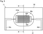
- Fig. 3 is a plan view showing part of the channel chip 11 according to the second embodiment.
- Fig. 4 is a schematic sectional view of the channel chip 11 taken along a line B-B shown in Fig. 3.
- Figs. 3 and 4 show only a liquid reservoir 40a and its surroundings in the channel chip 11.
- the channel chip 11 may include the liquid reservoir 40a in place of or in addition to the liquid reservoir 40 shown in Fig. 1 .
- the liquid reservoir 40a is capable of storing a liquid therein.
- the liquid reservoir 40a is configured with a through hole provided in the channel cover 25.
- the channel cover 25 has an opening 412a for injecting the liquid therethrough into the liquid reservoir 40a.
- the liquid reservoir 40a is configured as a recessed hole with an upper opening, rather than as an elongated tubular channel surrounded by walls on all sides like the inspection channel 41 shown in Fig. 1 or 2 .
- the channel chip 11 includes a pair of inspection electrodes 43c and 43d.
- Each of the inspection electrodes 43c and 43d includes a plurality of second thin line portions 433 arranged in a comb tooth shape.
- the second thin line portions 433 of the inspection electrodes 43c and 43d are arranged in equally spaced relation in the same manner as the second thin line portions 433 of the inspection electrodes 43a and 43b.
- the second thin line portions 433 are disposed between the liquid reservoir 40a and the substrate 21.
- the second thin line portions 433 are arranged so as to vertically overlap the liquid reservoir 40a.
- the inspection electrodes 43c and 43d are inspected for performance, whereby the performance of the main electrodes 33a and 33b is appropriately evaluated.
- the advance evaluation of the performance of the main electrodes 33a and 33b is made without using the main channel 31.
- the second overlapping portions 435 of the inspection electrodes 43c and 43d which vertically overlap the liquid reservoir 40a may be equal in area to the first overlapping portions 335 of the main electrodes 33a and 33b.
- the performance of the main electrodes 33a and 33b is appropriately evaluated from the inspection results of the inspection electrodes 43c and 43d.
- the inspection results of the inspection electrodes 43c and 43d may be corrected in accordance with liquid resistance or capacitance components dependent on the cross-sectional area of the channel immediately over the inspection electrodes 43c and 43d.
- the channel chip 11 may include a plurality of main channels 31 on the single substrate 21.
- the channel chip 11 may include a plurality of pairs of main electrodes 33a and 33b on the single substrate 21.
- the channel chip 11 may include a plurality of liquid reservoirs 40 (or liquid reservoirs 40a) on the single substrate 21. Also, the channel chip 11 may include the inspection electrodes 43a and 43b (or the inspection electrodes 43c and 43d) corresponding to each of the liquid reservoirs 40 (or the liquid reservoirs 40a).
- the shape of the electrode portions in the main electrodes 33a and 33b which exert an electrical action on the main channel 31 is not limited to the comb tooth shape shown in Fig. 1 , but may be changed as desired.
- the shape of the inspection electrodes 43a and 43b and the inspection electrodes 43c and 43d is not limited to the comb tooth shape, but may be changed as desired.
Landscapes
- Chemical & Material Sciences (AREA)
- Health & Medical Sciences (AREA)
- Life Sciences & Earth Sciences (AREA)
- Engineering & Computer Science (AREA)
- General Health & Medical Sciences (AREA)
- Bioinformatics & Cheminformatics (AREA)
- Chemical Kinetics & Catalysis (AREA)
- Molecular Biology (AREA)
- Zoology (AREA)
- Wood Science & Technology (AREA)
- Biotechnology (AREA)
- Organic Chemistry (AREA)
- Electrochemistry (AREA)
- Analytical Chemistry (AREA)
- Biochemistry (AREA)
- General Engineering & Computer Science (AREA)
- Physics & Mathematics (AREA)
- Medicinal Chemistry (AREA)
- Biomedical Technology (AREA)
- Microbiology (AREA)
- Sustainable Development (AREA)
- Genetics & Genomics (AREA)
- Hematology (AREA)
- Dispersion Chemistry (AREA)
- Microelectronics & Electronic Packaging (AREA)
- Clinical Laboratory Science (AREA)
- Fluid Mechanics (AREA)
- General Physics & Mathematics (AREA)
- Immunology (AREA)
- Pathology (AREA)
- Investigating Or Analyzing Materials By The Use Of Electric Means (AREA)
- Apparatus Associated With Microorganisms And Enzymes (AREA)
Abstract
Description
- The present invention relates to a channel chip and a dielectrophoresis device.
- Channel chips that use a dielectrophoretic force to separate and collect objects to be collected have been known in the past. This type of channel chip includes a channel (microchannel) into which a liquid containing the objects to be collected is injected, and electrodes (microelectrode) for electrically capturing the objects in the liquid. Such a channel chip is disclosed, for example, in Patent Literature 1.
- Patent Literature 1:
Japanese Patent Application Laid-Open No. 2017-134020 - Variations can occur in the thickness and relative dielectric constant of an insulating protective film for protecting in-plane electrodes and in the resistivity of electrode metal due to the manufacturing steps of the channel chip. If surface organic contamination occurs in the course of manufacture, organic residue thereof can also affect the dielectrophoretic force. There is a likelihood that these cause a reduction in dielectrophoretic force to such a degree that the objects to be collected cannot be captured or cause an excessive force to such a degree that the objects to be collected are damaged.
- For advance evaluation of the performance of the electrodes, it is also contemplated to inspect the electrodes for performance, with the liquid injected into the channel. However, the injection of the liquid into the channel might cause new surface contamination or cause clogging of the channel due to the presence of particles.
- It is an object of the present invention to provide a technique capable of evaluating the performance of electrodes for a channel for dielectrophoresis without using the channel.
- To solve the aforementioned problem, a first aspect is intended for a channel chip comprising: a substrate; a main channel disposed on one main surface of the substrate and capable of receiving a liquid therein; a liquid reservoir disposed on the main surface of the substrate in spaced apart relation to the main channel and capable of receiving a liquid therein; a pair of main electrodes disposed between the main surface of the substrate and the main channel; and at least one pair of inspection electrodes disposed between the main surface of the substrate and the liquid reservoir.
- A second aspect is intended for the channel chip of the first aspect, wherein the liquid reservoir includes an inspection channel capable of passing a liquid therethrough, and wherein the pair of inspection electrodes are disposed between the main surface of the substrate and the inspection channel.
- A third aspect is intended for the channel chip of the first or second aspect, wherein a first overlapping portion of the pair of main electrodes which overlaps the main channel is equal in area to a second overlapping portion of the pair of inspection electrodes which overlaps the liquid reservoir.
- A fourth aspect is intended for the channel chip of any one of the first to third aspects, wherein the at least one pair of inspection electrode includes not less than two pairs of inspection electrodes.
- A fifth aspect is intended for the channel chip of the fourth aspect, wherein the at least one pair of inspection electrodes include three pairs of inspection electrodes.
- A sixth aspect is intended for the channel chip of any one of the first to fifth aspects, wherein the pair of main electrodes and the pair of inspection electrodes are disposed adjacent to each other.
- A seventh aspect is intended for the channel chip of any one of the first to sixth aspects, wherein the pair of main electrodes and the pair of inspection electrodes have respective surfaces covered with an insulating protective film, and wherein the main channel and the liquid reservoir are disposed on the insulating protective film.
- An eighth aspect is intended for the channel chip of any one of the first to seventh aspects, wherein the pair of main electrodes and the pair of inspection electrodes have a comb tooth shape.
- A ninth aspect is intended for a dielectrophoresis device comprising: a channel chip as recited in any one of the first to eighth aspects; and a power supply part for applying a voltage to the pair of main electrodes and the pair of inspection electrodes.
- According to the channel chip of the first aspect, the pair of main electrodes corresponding to the main channel and the pair of inspection electrodes corresponding to the liquid reservoir are disposed on the same substrate. Thus, with the liquid injected in the liquid reservoir, the pair of inspection electrodes are inspected for performance, whereby the performance of the pair of main electrodes is appropriately evaluated without using the main channel and the pair of main electrodes.
- According to the channel chip of the second aspect, the pair of inspection electrodes overlap the inspection channel of the liquid reservoir, whereby the conditions of the environment in which the pair of inspection electrodes are disposed are brought closer to the conditions of the environment in which the pair of main electrodes are disposed. Thus, the performance of the pair of main electrodes is appropriately evaluated based on the inspection results of the pair of inspection electrodes.
- According to the channel chip of the third aspect, the performance of the pair of inspection electrodes is the same as that of the pair of main electrodes because the area of the second overlapping portion of the pair of inspection electrodes is equal to that of the first overlapping portion of the pair of main electrodes. Thus, the performance of the pair of main electrodes is appropriately evaluated based on the inspection results of the pair of inspection electrodes.
- According to the channel chip of the fourth aspect, even if in-plane variations occur in the manufacturing steps within the same channel chip, the performance of the pair of main electrodes is appropriately evaluated by averaging the measurement results of the plurality of pairs of inspection electrodes.
- According to the channel chip of the fifth aspect, the provision of the three pairs of inspection electrodes ensures the minimum number of samples required to obtain an average error and suppresses an increase in size of the channel chip.
- According to the channel chip of the sixth aspect, the pair of main electrodes and the pair of inspection electrodes are disposed adjacent to each other, so that the conditions of the environment in which the pair of inspection electrodes are disposed are brought closer to the conditions of the environment in which the pair of main electrodes are disposed. Thus, the performance of the pair of main electrodes is appropriately evaluated based on the inspection results of the pair of inspection electrodes.
- According to the channel chip of the seventh aspect, the pair of main electrodes and the pair of inspection electrodes are protected by the insulating protective film.
- According to the channel chip of the eighth aspect, the pair of main electrodes and the inspection electrodes are in a shortened and parallel comb tooth shape, whereby the low-resistance and uniform dielectrophoretic force is applied into the liquid.
-
- [
fig. 1] Fig. 1 is a plan view showing a dielectrophoresis device according to a first embodiment. - [
fig. 2] Fig. 2 is a schematic sectional view of a channel chip taken along a line A-A shown inFig. 1 . - [
fig. 3] Fig. 3 is a plan view showing part of the channel chip according to a second embodiment. - [
fig. 4] Fig. 4 is a schematic sectional view of the channel chip taken along a line B-B shown inFig. 3 . - Embodiments according to the present invention will now be described with reference to the accompanying drawings. Components described in the embodiments are merely illustrative, and there is no intention to limit the scope of the present invention only thereto. In the drawings, the dimensions of components and the number of components are shown in exaggeration or in simplified form, as appropriate, for the sake of easier understanding in some cases.
-
Fig. 1 is a plan view showing a dielectrophoresis device 1 according to a first embodiment.Fig. 2 is a schematic sectional view of achannel chip 11 taken along a line A-A shown inFig. 1 . As shown inFig. 1 , the dielectrophoresis device 1 includes thechannel chip 11, a plurality ofpower supply parts 13, and acontroller 15. - The
channel chip 11 is a device for electrically separating and collecting objects to be collected that are contained in a liquid of a specimen. Conceivable examples of the liquid of the specimen include body fluids such as blood, and physiological saline solution. The objects to be collected are substances present in liquids, and conceivable specific examples thereof include microorganisms, cells, proteins, and nucleic acids. Thepower supply parts 13 apply voltage to respective electrodes disposed in thechannel chip 11. Thecontroller 15 controls the voltage applied by thepower supply parts 13. Thecontroller 15 is configured with a computer having a general-purpose processor such as a CPU, a RAM, and the like. Thecontroller 15 may include a purpose-built circuit (such as an application specific integrated circuit (ASIC)). - As shown in
Fig. 1 , thechannel chip 11 includes asubstrate 21, amain channel 31, a pair ofmain electrodes liquid reservoir 40, and a plurality of pairs (in this embodiment, three pairs) ofinspection electrodes - The
substrate 21 is made of quartz glass, for example. However, the material of thesubstrate 21 is not limited to quartz glass, and may be selected as appropriate. Thesubstrate 21 has a substantially rectangular planar shape. However, the shape of thesubstrate 21 is not limited to the substantially rectangular planar shape. - The
main channel 31 is capable of receiving therein a liquid containing the objects to be collected. As shown inFig. 1 , themain channel 31 includes aseparation channel 311 and a pair ofcollection channels separation channel 311 is an elongated channel extending linearly. Theseparation channel 311 has a first end connected to afirst supply part 315. Thefirst supply part 315 has afirst supply opening 316 for injecting therethrough a liquid to flow into theseparation channel 311. At a second end of theseparation channel 311, themain channel 31 branches into thecollection channel 313a and thecollection channel 313b. - The
collection channel 313a is a channel for collecting the objects to be collected that flow through theseparation channel 311. Thecollection channel 313b is a channel for collecting objects not to be collected that flow through theseparation channel 311. Each of thecollection channels separation channel 311. Thecollection channel 313a has a second end connected to afirst collection part 317a. Thecollection channel 313b has a second end connected afirst collection part 317b. Thefirst collection part 317a has a first collection opening 318 for collecting the liquid flowing through thecollection channel 313a. Thefirst collection part 317b has a first collection opening 318 for collecting the liquid flowing through thecollection channel 313b. - As shown in
Fig. 2 , themain electrodes upper surface 211 of thesubstrate 21. Themain electrodes protective film 23. The insulatingprotective film 23 is, for example, an oxide film (such as a silicon oxide film (SiOx)). It should be noted that the insulatingprotective film 23 may be a nitride film (such as a silicon nitride film). Themain electrodes protective film 23, which in turn suppresses electrochemical reactions occurring at an interface between the electrode metal and the liquid to suppress deterioration and wear of the electrode metal over time. - A
channel cover 25 is disposed on an upper surface of the insulatingprotective film 23. Thechannel cover 25 is made of PDMS (dimethylpolysiloxane), for example. Thechannel cover 25 has a lower surface with an elongated recessedchannel groove 251. The width of thechannel groove 251 is, for example, on a microscale. Thechannel groove 251 of thechannel cover 25 and the upper surface of the insulatingprotective film 23 define themain channel 31 and aninspection channel 41 to be described later. In this manner, thechannel cover 25 is mounted to theupper surface 211 of the substrate 2, whereby themain channel 31 is disposed on theupper surface 211 of thesubstrate 21. As shown inFig. 1 , thesubstrate 21 is wider than thechannel cover 25. - As shown in
Fig. 1 , each of themain electrodes first pad portion 331 spaced apart from themain channel 31, and a plurality of firstthin line portions 333 arranged in a comb tooth shape. At least part of thefirst pad portion 331 of each of themain electrodes channel cover 25. Thefirst pad portion 331 of each of themain electrodes protective film 23. This enables thepower supply parts 13 to be connected to thefirst pad portions 331 or enables thefirst pad portions 331 to be grounded outside thechannel cover 25. - The first
thin line portions 333 of themain electrodes main channel 31. The firstthin line portions 333 of themain electrodes separation channel 311 of themain channel 31. - The first
thin line portions 333 are in the shape of thin lines extending in a direction intersecting theseparation channel 311 of themain channel 31. The firstthin line portions 333 of themain electrodes separation channel 311. The firstthin line portions 333 of themain electrode 33a and the firstthin line portions 333 of themain electrodes 33b are spaced one from another and arranged alternately in the longitudinal direction of theseparation channel 311. Specifically, 20 pairs of the firstthin line portions 333 of themain electrode 33a and themain electrode 33b are arranged alternately at spacings of 50 µm in the longitudinal direction of theseparation channel 311. It should be noted that the spacings at which the firstthin line portions 333 are arranged and the number of pairs of firstthin line portions 333 may be set arbitrarily. - Each of the first
thin line portions 333 of themain electrodes separation channel 311 so as to form an acute angle, for example, in the range of 10° to 60° with respect to the longitudinal direction of theseparation channel 311. - In using the dielectrophoresis device 1, a liquid containing the objects to be collected is supplied from the
first supply part 315 to themain channel 31. Then, as shown inFig. 1 , thefirst pad portion 331 of themain electrode 33a is grounded, and apower supply part 13 is connected to thefirst pad portion 331 of themain electrode 33b. Thepower supply part 13 is configured with a function generator, for example. Thepower supply part 13 applies an AC voltage between themain electrodes controller 15. Specifically, the AC voltage in accordance with the objects to be collected is a voltage with a frequency that generates an electric field specifically exerting a dielectrophoretic force (attraction) on the objects to be collected, and with a magnitude to such a degree as not to destroy the objects to be collected. - When the voltage is applied between the
main electrodes main channel 31 are collected into thecollection channel 313a by flowing through themain channel 31 while being attracted to the firstthin line portions 333 of themain electrodes collection channel 313b. - The
liquid reservoir 40 is capable of storing a liquid therein. As shown inFig. 1 , theliquid reservoir 40 includes theinspection channel 41. Theliquid reservoir 40 and theinspection channel 41 are disposed on the insulatingprotective film 23 in the same manner as themain channel 31 shown inFig. 2 . As shown inFig. 1 , theinspection channel 41 has an elongated linear shape. Theinspection channel 41 has a first end connected to asecond supply part 411. Thesecond supply part 411 has asecond supply opening 412 for supplying a liquid to flow into theinspection channel 41. Theinspection channel 41 has a second end connected to asecond collection part 413. Thesecond collection part 413 has a second collection opening 414 for collecting the liquid flowing through theinspection channel 41. - As shown in
Fig. 1 , the three pairs ofinspection electrodes same substrate 21 as themain electrodes inspection electrodes main electrodes inspection electrodes upper surface 211 of thesubstrate 21 in the same manner as themain electrodes Fig. 2 . Theinspection electrodes upper surface 211 of thesubstrate 21 and theliquid reservoir 40. Theinspection electrodes protective film 23. This suppresses electrochemical reactions occurring at an interface between the electrode metal and the liquid in theinspection electrodes - As shown in
Fig. 1 , each of theinspection electrodes second pad portion 431 spaced apart from themain channel 31, and a plurality of secondthin line portions 433 arranged in a comb tooth shape. As shown inFig. 1 , thesecond pad portion 431 is disposed outside thechannel cover 25. Thesecond pad portion 431 of each of theinspection electrodes protective film 23. This enables thepower supply parts 13 to be connected to thesecond pad portions 431 or enables thesecond pad portions 431 to be grounded outside thechannel cover 25. - The second
thin line portions 433 of theinspection electrodes inspection channel 41. The secondthin line portions 433 of theinspection electrodes inspection channel 41. - The second
thin line portions 433 are in the shape of thin lines extending in a direction intersecting (in this embodiment, orthogonal to) theinspection channel 41. The secondthin line portions 433 of theinspection electrodes inspection channel 41. The secondthin line portions 433 of theinspection electrodes 43a and the secondthin line portions 433 of theinspection electrodes 43b are spaced one from another and arranged alternately in the longitudinal direction of theinspection channel 41. - Portions (first overlapping portions 335) of the
main electrodes main channel 31 are preferably equal in area to portions (second overlapping portions 435) of theinspection electrodes inspection channel 41. The spacings at which theinspection electrodes inspection electrodes portions 335 is equal to the area of the second overlappingportions 435. - Each of the second
thin line portions 433 of theinspection electrodes inspection channel 41 in the same manner as the firstthin line portions 333 of themain electrodes - Subsequently, a method of manufacturing the
channel chip 11 will be described. First, a film of electrode metal having a predetermined thickness (e.g., 100 nm) is deposited on theupper surface 211 of thesubstrate 21 by vacuum evaporation. Then, a predetermined pattern is formed on the film of electrode metal by photolithography and wet etching. This patterning forms themain electrodes inspection electrodes upper surface 211 of thesubstrate 21. After the patterning of the electrodes, the insulatingprotective film 23 is formed. Specifically, a silicon oxide film (SiOx) that is the insulatingprotective film 23 having a predetermined thickness (e.g., 200 nm) is deposited on theupper surface 211 of thesubstrate 21 and on the upper surfaces of the electrodes (including themain electrodes inspection electrodes - After the insulating
protective film 23 is formed, thefirst pad portion 331 of each of themain electrodes second pad portion 431 of each of theinspection electrodes channel cover 25 is mounted to thesubstrate 21. Specifically, thechannel cover 25 and thesubstrate 21 on which the electrodes are formed are plasma-treated and affixed together. Thechannel groove 251 corresponding to themain channel 31 and a channel groove corresponding to the liquid reservoir 40 (the inspection channel 41) are formed in thechannel cover 25. Thus, the mounting of thechannel cover 25 forms themain channel 31 and theliquid reservoir 40 on thesubstrate 21. - In the case of the
channel chip 11, themain electrodes main channel 31 and theinspection electrodes liquid reservoir 40 are disposed on thesame substrate 21. Thus, with the liquid received in theliquid reservoir 40, theinspection electrodes main electrodes main channel 31 is appropriately evaluated without using themain channel 31. This suppresses contamination of themain channel 31 and clogging of the main electrodes 33 in order to evaluate the performance of themain electrodes - In the
channel chip 11, variations in manufacturing steps of the channel chip 11 (variations in the thickness or relative dielectric constant of the insulating protective film, and variations in the resistivity of the electrode metal) and the presence of defects such as surface organic contamination and electrode breakage are detected by inspecting theinspection electrodes good channel chips 11 to be provided to users is increased by inspecting theinspection electrodes - The
inspection electrodes inspection channel 41 of theliquid reservoir 40, whereby the conditions of the environment in which theinspection electrodes main electrodes main electrodes inspection electrodes - As shown in
Fig. 1 , theinspection electrodes main electrodes inspection electrodes main electrodes main electrodes inspection electrodes - If the cross-sectional shape and cross-sectional dimensions of the
inspection channel 41 are the same as those of theseparation channel 311 in themain channel 31, the cross-sectional dimensions between the electrodes including the liquid of theinspection electrodes main electrodes separation channel 311. This allows theinspection electrodes main electrodes main electrodes inspection electrodes - The
main electrodes inspection electrodes - The performance of the
inspection electrodes main electrodes portions 435 of theinspection electrodes portions 335 of themain electrodes main electrodes main channel 31 is appropriately evaluated based on the inspection results of theinspection electrodes - It is not essential that the area of the first overlapping
portions 335 is equal to the area of the second overlappingportions 435. Even if the area of the first overlappingportions 335 is different from the area of the second overlappingportions 435, themain electrodes inspection electrodes - The
channel chip 11 includes the plurality of pairs ofinspection electrodes same channel chip 11, the performance of themain electrodes inspection electrodes inspection electrodes channel chip 11. - In the example shown in
Fig. 1 , thechannel chip 11 includes the three pairs ofinspection electrodes channel chip 11 may include only two pairs ofinspection electrodes inspection electrodes channel chip 11 includes the plurality of pairs ofinspection electrodes channel chip 11 may include only one pair ofinspection electrodes channel chip 11 includes only one pair ofinspection electrodes channel chip 11 is reduced. - It is desirable that the three pairs of
inspection electrodes main electrodes main electrodes inspection electrodes - A correction value for correction of manufacturing variations is obtained based on the inspection results of the
inspection electrodes controller 15 may control thepower supply parts 13 so that thepower supply parts 13 apply a voltage between themain electrodes main channel 31. - Next, a second embodiment will be described. In the following description, components having the same functions as those described above are designated by like reference numerals and characters or like reference numerals and characters with alphabetic characters appended thereto, and will not be described in detail in some cases.
-
Fig. 3 is a plan view showing part of thechannel chip 11 according to the second embodiment.Fig. 4 is a schematic sectional view of thechannel chip 11 taken along a line B-B shown inFig. 3. Figs. 3 and4 show only aliquid reservoir 40a and its surroundings in thechannel chip 11. - As shown in
Figs. 3 and4 , thechannel chip 11 may include theliquid reservoir 40a in place of or in addition to theliquid reservoir 40 shown inFig. 1 . Theliquid reservoir 40a is capable of storing a liquid therein. As shown inFig. 4 , theliquid reservoir 40a is configured with a through hole provided in thechannel cover 25. Thechannel cover 25 has anopening 412a for injecting the liquid therethrough into theliquid reservoir 40a. Theliquid reservoir 40a is configured as a recessed hole with an upper opening, rather than as an elongated tubular channel surrounded by walls on all sides like theinspection channel 41 shown inFig. 1 or2 . - As shown in
Figs. 3 and4 , thechannel chip 11 includes a pair ofinspection electrodes inspection electrodes thin line portions 433 arranged in a comb tooth shape. The secondthin line portions 433 of theinspection electrodes thin line portions 433 of theinspection electrodes thin line portions 433 are disposed between theliquid reservoir 40a and thesubstrate 21. The secondthin line portions 433 are arranged so as to vertically overlap theliquid reservoir 40a. - In the case of the
channel chip 11 according to the second embodiment, with the liquid injected into theliquid reservoir 40a, theinspection electrodes main electrodes main electrodes main channel 31. - The second overlapping
portions 435 of theinspection electrodes liquid reservoir 40a may be equal in area to the first overlappingportions 335 of themain electrodes main electrodes inspection electrodes inspection electrodes inspection electrodes - While the embodiments have been described hereinabove, the present invention is not limited to the aforementioned embodiments, but various modifications may be made.
- For example, the
channel chip 11 may include a plurality ofmain channels 31 on thesingle substrate 21. Alternatively, thechannel chip 11 may include a plurality of pairs ofmain electrodes single substrate 21. - The
channel chip 11 may include a plurality of liquid reservoirs 40 (orliquid reservoirs 40a) on thesingle substrate 21. Also, thechannel chip 11 may include theinspection electrodes inspection electrodes liquid reservoirs 40a). - The shape of the electrode portions in the
main electrodes main channel 31 is not limited to the comb tooth shape shown inFig. 1 , but may be changed as desired. Likewise, the shape of theinspection electrodes inspection electrodes - While the invention has been described in detail, the foregoing description is in all aspects illustrative, and the invention is not limited thereto. It is therefore understood that numerous modifications and variations not illustrated can be devised without departing from the scope of the invention. The components described in the aforementioned embodiments and in the various modifications may be combined together or dispensed with, as appropriate, unless the components are inconsistent with each other.
-
- 1 Dielectrophoresis device
- 11 Channel chip
- 21 Substrate
- 23 Insulating protective film
- 31 Main channel
- 33a, 33b Main electrodes
- 40, 40a Liquid reservoirs
- 41 Inspection channel
- 43a, 43b Inspection electrodes
- 43c, 43d Inspection electrodes
- 211 Upper surface (main surface)
- 335 First overlapping portions
- 412a Opening
- 435 Second overlapping portions
Claims (9)
- A channel chip comprising:a substrate;a main channel disposed on one main surface of said substrate and capable of receiving a liquid therein;a liquid reservoir disposed on said main surface of said substrate in spaced apart relation to said main channel and capable of receiving a liquid therein;a pair of main electrodes disposed between said main surface of said substrate and said main channel; andat least one pair of inspection electrodes disposed between said main surface of said substrate and said liquid reservoir.
- The channel chip according to Claim 1,wherein said liquid reservoir includes an inspection channel capable of passing a liquid therethrough, andwherein said pair of inspection electrodes are disposed between said main surface of said substrate and said inspection channel.
- The channel chip according to Claim 1 or 2,
wherein a first overlapping portion of said pair of main electrodes which overlaps said main channel is equal in area to a second overlapping portion of said pair of inspection electrodes which overlaps said liquid reservoir. - The channel chip according to any one of Claims 1 to 3,
wherein said at least one pair of inspection electrodes include not less than two pairs of inspection electrodes. - The channel chip according to Claim 4,
wherein said at least one pair of inspection electrodes include three pairs of inspection electrodes. - The channel chip according to any one of Claims 1 to 5,
wherein said pair of main electrodes and said pair of inspection electrodes are disposed adjacent to each other. - The channel chip according to any one of Claims 1 to 6,wherein said pair of main electrodes and said pair of inspection electrodes have respective surfaces covered with an insulating protective film, andwherein said main channel and said liquid reservoir are disposed on said insulating protective film.
- The channel chip according to any one of Claims 1 to 7,
wherein said pair of main electrodes and said pair of inspection electrodes have a comb tooth shape. - A dielectrophoresis device comprising:a channel chip as recited in any one of Claims 1 to 8; anda power supply part for applying a voltage to said pair of main electrodes and said pair of inspection electrodes.
Applications Claiming Priority (2)
| Application Number | Priority Date | Filing Date | Title |
|---|---|---|---|
| JP2021108280A JP7662433B2 (en) | 2021-06-30 | 2021-06-30 | Flow channel chip and dielectrophoresis device |
| PCT/JP2022/026048 WO2023277088A1 (en) | 2021-06-30 | 2022-06-29 | Fluidic chip and dielectrophoresis device |
Publications (2)
| Publication Number | Publication Date |
|---|---|
| EP4365581A1 true EP4365581A1 (en) | 2024-05-08 |
| EP4365581A4 EP4365581A4 (en) | 2025-07-02 |
Family
ID=84691822
Family Applications (1)
| Application Number | Title | Priority Date | Filing Date |
|---|---|---|---|
| EP22833234.2A Pending EP4365581A4 (en) | 2021-06-30 | 2022-06-29 | FLUIDIC CHIP AND DIELECTROPHORESIS DEVICE |
Country Status (5)
| Country | Link |
|---|---|
| US (1) | US20260115737A1 (en) |
| EP (1) | EP4365581A4 (en) |
| JP (1) | JP7662433B2 (en) |
| CN (1) | CN117597581A (en) |
| WO (1) | WO2023277088A1 (en) |
Families Citing this family (3)
| Publication number | Priority date | Publication date | Assignee | Title |
|---|---|---|---|---|
| JP2024116726A (en) * | 2023-02-16 | 2024-08-28 | 株式会社Screenホールディングス | Channel chip and method for manufacturing the channel chip |
| JP2025103465A (en) * | 2023-12-27 | 2025-07-09 | 株式会社Screenホールディングス | Separation Chip |
| JP2025148640A (en) | 2024-03-26 | 2025-10-08 | 株式会社Screenホールディングス | Control voltage correction method and dielectrophoresis device |
Family Cites Families (9)
| Publication number | Priority date | Publication date | Assignee | Title |
|---|---|---|---|---|
| US20060177815A1 (en) * | 2004-11-29 | 2006-08-10 | The Regents Of The University Of California | Dielectrophoretic particle sorter |
| JP2006351246A (en) * | 2005-06-13 | 2006-12-28 | Fuji Xerox Co Ltd | Power converter and its manufacturing method |
| JP4517980B2 (en) * | 2005-08-23 | 2010-08-04 | 株式会社島津製作所 | Particle measuring device |
| WO2007046484A1 (en) * | 2005-10-19 | 2007-04-26 | Sharp Kabushiki Kaisha | Electrophoretic chip, electrophoretic device, and electrophoretic system |
| JP6441838B2 (en) | 2016-01-29 | 2018-12-19 | 株式会社Afiテクノロジー | Analysis device and separation device |
| US9873129B1 (en) * | 2016-12-19 | 2018-01-23 | Charlot Biosciences, Inc. | Multi-planar microelectrode array device and methods of making and using same |
| JP6871116B2 (en) * | 2017-09-15 | 2021-05-12 | 株式会社東芝 | Cell sorter |
| JP6941840B2 (en) * | 2018-07-11 | 2021-09-29 | シャープ株式会社 | Particle separator |
| GB2577074B (en) * | 2018-09-12 | 2022-06-01 | Quantumdx Group Ltd | Microfluidic device with DEP arrays |
-
2021
- 2021-06-30 JP JP2021108280A patent/JP7662433B2/en active Active
-
2022
- 2022-06-29 US US18/575,193 patent/US20260115737A1/en active Pending
- 2022-06-29 CN CN202280046916.3A patent/CN117597581A/en active Pending
- 2022-06-29 EP EP22833234.2A patent/EP4365581A4/en active Pending
- 2022-06-29 WO PCT/JP2022/026048 patent/WO2023277088A1/en not_active Ceased
Also Published As
| Publication number | Publication date |
|---|---|
| CN117597581A (en) | 2024-02-23 |
| WO2023277088A1 (en) | 2023-01-05 |
| JP7662433B2 (en) | 2025-04-15 |
| EP4365581A4 (en) | 2025-07-02 |
| US20260115737A1 (en) | 2026-04-30 |
| JP2023005958A (en) | 2023-01-18 |
Similar Documents
| Publication | Publication Date | Title |
|---|---|---|
| US20260115737A1 (en) | Channel chip and dielectrophoresis device | |
| Truman et al. | Monitoring liquid transport and chemical composition in lab on a chip systems using ion sensitive FET devices | |
| KR100316437B1 (en) | Electrochemical detector integrated on microfabricated capillary electrophoresis chips | |
| JP5894798B2 (en) | Detector system and method | |
| US20160290957A1 (en) | Nanoelectronic sensor pixel | |
| US10379102B2 (en) | System and method for single molecule detection | |
| WO2012078340A1 (en) | Reliable nanofet biosensor process with high-k dielectric | |
| MX2015004671A (en) | Wide dynamic range fluid sensor based on nanowire platform. | |
| WO2016009673A1 (en) | Particle inspection system and driving method employed therein | |
| JP2009014342A (en) | Dielectrophoresis chip, dielectrophoresis apparatus, and dielectrophoresis system | |
| Solsona et al. | Gradient in the electric field for particle position detection in microfluidic channels | |
| US7635420B1 (en) | Dielectrophoresis-based particle sensor using nanoelectrode arrays | |
| KR101749600B1 (en) | Sample concentrator and method for extracting sample concentrated using the same | |
| TWI499778B (en) | Micro-fluid device | |
| Li et al. | Changing the Blood Test: Accurate Determination of Mercury (II) in One Microliter of Blood Using Oriented ZnO Nanobelt Array Film Solution‐Gated Transistor Chips | |
| KR20180109647A (en) | Single point detection type microfluidic isoelectric focusing assay and chips using the same | |
| EP4365582A1 (en) | Flow channel chip and separation system | |
| CN100417937C (en) | Chip Capacitively Coupled Non-Contact Conductivity Detector | |
| Qi et al. | A nanofluidic sensor for real-time detection of ultratrace contaminant particles in IC fabrication | |
| CN104620099B (en) | Sample-dependent selection of parameters for use in electrokinetic processing of samples | |
| JP6831521B2 (en) | Analytical element and analyzer | |
| KR20200129850A (en) | Bio-sensing device | |
| JP2023005959A (en) | Flow passage type device | |
| US9250207B2 (en) | Controlled translocation of macromolecules employing a funnel nanopore structure and a gel | |
| EP4563229A1 (en) | Channel chip, dielectrophoretic device, and control voltage correction method |
Legal Events
| Date | Code | Title | Description |
|---|---|---|---|
| STAA | Information on the status of an ep patent application or granted ep patent |
Free format text: STATUS: THE INTERNATIONAL PUBLICATION HAS BEEN MADE |
|
| PUAI | Public reference made under article 153(3) epc to a published international application that has entered the european phase |
Free format text: ORIGINAL CODE: 0009012 |
|
| STAA | Information on the status of an ep patent application or granted ep patent |
Free format text: STATUS: REQUEST FOR EXAMINATION WAS MADE |
|
| 17P | Request for examination filed |
Effective date: 20231211 |
|
| AK | Designated contracting states |
Kind code of ref document: A1 Designated state(s): AL AT BE BG CH CY CZ DE DK EE ES FI FR GB GR HR HU IE IS IT LI LT LU LV MC MK MT NL NO PL PT RO RS SE SI SK SM TR |
|
| DAV | Request for validation of the european patent (deleted) | ||
| DAX | Request for extension of the european patent (deleted) | ||
| A4 | Supplementary search report drawn up and despatched |
Effective date: 20250602 |
|
| RIC1 | Information provided on ipc code assigned before grant |
Ipc: B03C 5/02 20060101ALI20250526BHEP Ipc: B03C 5/00 20060101ALI20250526BHEP Ipc: B01L 3/00 20060101ALI20250526BHEP Ipc: G01N 27/447 20060101ALI20250526BHEP Ipc: C12M 1/34 20060101ALI20250526BHEP Ipc: C12M 1/00 20060101ALI20250526BHEP Ipc: G01N 27/00 20060101AFI20250526BHEP |