EP4365457A1 - Rolling bearing - Google Patents
Rolling bearing Download PDFInfo
- Publication number
- EP4365457A1 EP4365457A1 EP22833338.1A EP22833338A EP4365457A1 EP 4365457 A1 EP4365457 A1 EP 4365457A1 EP 22833338 A EP22833338 A EP 22833338A EP 4365457 A1 EP4365457 A1 EP 4365457A1
- Authority
- EP
- European Patent Office
- Prior art keywords
- resistor
- detector element
- disposed
- circumferential direction
- detector
- Prior art date
- Legal status (The legal status is an assumption and is not a legal conclusion. Google has not performed a legal analysis and makes no representation as to the accuracy of the status listed.)
- Granted
Links
Images




Classifications
-
- F—MECHANICAL ENGINEERING; LIGHTING; HEATING; WEAPONS; BLASTING
- F16—ENGINEERING ELEMENTS AND UNITS; GENERAL MEASURES FOR PRODUCING AND MAINTAINING EFFECTIVE FUNCTIONING OF MACHINES OR INSTALLATIONS; THERMAL INSULATION IN GENERAL
- F16C—SHAFTS; FLEXIBLE SHAFTS; ELEMENTS OR CRANKSHAFT MECHANISMS; ROTARY BODIES OTHER THAN GEARING ELEMENTS; BEARINGS
- F16C41/00—Other accessories, e.g. devices integrated in the bearing not relating to the bearing function as such
-
- F—MECHANICAL ENGINEERING; LIGHTING; HEATING; WEAPONS; BLASTING
- F16—ENGINEERING ELEMENTS AND UNITS; GENERAL MEASURES FOR PRODUCING AND MAINTAINING EFFECTIVE FUNCTIONING OF MACHINES OR INSTALLATIONS; THERMAL INSULATION IN GENERAL
- F16C—SHAFTS; FLEXIBLE SHAFTS; ELEMENTS OR CRANKSHAFT MECHANISMS; ROTARY BODIES OTHER THAN GEARING ELEMENTS; BEARINGS
- F16C19/00—Bearings with rolling contact, for exclusively rotary movement
- F16C19/02—Bearings with rolling contact, for exclusively rotary movement with bearing balls essentially of the same size in one or more circular rows
-
- F—MECHANICAL ENGINEERING; LIGHTING; HEATING; WEAPONS; BLASTING
- F16—ENGINEERING ELEMENTS AND UNITS; GENERAL MEASURES FOR PRODUCING AND MAINTAINING EFFECTIVE FUNCTIONING OF MACHINES OR INSTALLATIONS; THERMAL INSULATION IN GENERAL
- F16C—SHAFTS; FLEXIBLE SHAFTS; ELEMENTS OR CRANKSHAFT MECHANISMS; ROTARY BODIES OTHER THAN GEARING ELEMENTS; BEARINGS
- F16C19/00—Bearings with rolling contact, for exclusively rotary movement
- F16C19/02—Bearings with rolling contact, for exclusively rotary movement with bearing balls essentially of the same size in one or more circular rows
- F16C19/04—Bearings with rolling contact, for exclusively rotary movement with bearing balls essentially of the same size in one or more circular rows for radial load mainly
- F16C19/06—Bearings with rolling contact, for exclusively rotary movement with bearing balls essentially of the same size in one or more circular rows for radial load mainly with a single row or balls
-
- F—MECHANICAL ENGINEERING; LIGHTING; HEATING; WEAPONS; BLASTING
- F16—ENGINEERING ELEMENTS AND UNITS; GENERAL MEASURES FOR PRODUCING AND MAINTAINING EFFECTIVE FUNCTIONING OF MACHINES OR INSTALLATIONS; THERMAL INSULATION IN GENERAL
- F16C—SHAFTS; FLEXIBLE SHAFTS; ELEMENTS OR CRANKSHAFT MECHANISMS; ROTARY BODIES OTHER THAN GEARING ELEMENTS; BEARINGS
- F16C19/00—Bearings with rolling contact, for exclusively rotary movement
- F16C19/52—Bearings with rolling contact, for exclusively rotary movement with devices affected by abnormal or undesired conditions
-
- F—MECHANICAL ENGINEERING; LIGHTING; HEATING; WEAPONS; BLASTING
- F16—ENGINEERING ELEMENTS AND UNITS; GENERAL MEASURES FOR PRODUCING AND MAINTAINING EFFECTIVE FUNCTIONING OF MACHINES OR INSTALLATIONS; THERMAL INSULATION IN GENERAL
- F16C—SHAFTS; FLEXIBLE SHAFTS; ELEMENTS OR CRANKSHAFT MECHANISMS; ROTARY BODIES OTHER THAN GEARING ELEMENTS; BEARINGS
- F16C19/00—Bearings with rolling contact, for exclusively rotary movement
- F16C19/52—Bearings with rolling contact, for exclusively rotary movement with devices affected by abnormal or undesired conditions
- F16C19/522—Bearings with rolling contact, for exclusively rotary movement with devices affected by abnormal or undesired conditions related to load on the bearing, e.g. bearings with load sensors or means to protect the bearing against overload
-
- F—MECHANICAL ENGINEERING; LIGHTING; HEATING; WEAPONS; BLASTING
- F16—ENGINEERING ELEMENTS AND UNITS; GENERAL MEASURES FOR PRODUCING AND MAINTAINING EFFECTIVE FUNCTIONING OF MACHINES OR INSTALLATIONS; THERMAL INSULATION IN GENERAL
- F16C—SHAFTS; FLEXIBLE SHAFTS; ELEMENTS OR CRANKSHAFT MECHANISMS; ROTARY BODIES OTHER THAN GEARING ELEMENTS; BEARINGS
- F16C33/00—Parts of bearings; Special methods for making bearings or parts thereof
- F16C33/30—Parts of ball or roller bearings
- F16C33/58—Raceways; Race rings
-
- F—MECHANICAL ENGINEERING; LIGHTING; HEATING; WEAPONS; BLASTING
- F16—ENGINEERING ELEMENTS AND UNITS; GENERAL MEASURES FOR PRODUCING AND MAINTAINING EFFECTIVE FUNCTIONING OF MACHINES OR INSTALLATIONS; THERMAL INSULATION IN GENERAL
- F16C—SHAFTS; FLEXIBLE SHAFTS; ELEMENTS OR CRANKSHAFT MECHANISMS; ROTARY BODIES OTHER THAN GEARING ELEMENTS; BEARINGS
- F16C33/00—Parts of bearings; Special methods for making bearings or parts thereof
- F16C33/30—Parts of ball or roller bearings
- F16C33/58—Raceways; Race rings
- F16C33/583—Details of specific parts of races
- F16C33/586—Details of specific parts of races outside the space between the races, e.g. end faces or bore of inner ring
-
- G—PHYSICS
- G01—MEASURING; TESTING
- G01L—MEASURING FORCE, STRESS, TORQUE, WORK, MECHANICAL POWER, MECHANICAL EFFICIENCY, OR FLUID PRESSURE
- G01L1/00—Measuring force or stress, in general
- G01L1/20—Measuring force or stress, in general by measuring variations in ohmic resistance of solid materials or of electrically-conductive fluids; by making use of electrokinetic cells, i.e. liquid-containing cells wherein an electrical potential is produced or varied upon the application of stress
- G01L1/22—Measuring force or stress, in general by measuring variations in ohmic resistance of solid materials or of electrically-conductive fluids; by making use of electrokinetic cells, i.e. liquid-containing cells wherein an electrical potential is produced or varied upon the application of stress using resistance strain gauges
-
- G—PHYSICS
- G01—MEASURING; TESTING
- G01L—MEASURING FORCE, STRESS, TORQUE, WORK, MECHANICAL POWER, MECHANICAL EFFICIENCY, OR FLUID PRESSURE
- G01L5/00—Apparatus for, or methods of, measuring force, work, mechanical power, or torque, specially adapted for specific purposes
-
- G—PHYSICS
- G01—MEASURING; TESTING
- G01L—MEASURING FORCE, STRESS, TORQUE, WORK, MECHANICAL POWER, MECHANICAL EFFICIENCY, OR FLUID PRESSURE
- G01L5/00—Apparatus for, or methods of, measuring force, work, mechanical power, or torque, specially adapted for specific purposes
- G01L5/0009—Force sensors associated with a bearing
-
- G—PHYSICS
- G01—MEASURING; TESTING
- G01L—MEASURING FORCE, STRESS, TORQUE, WORK, MECHANICAL POWER, MECHANICAL EFFICIENCY, OR FLUID PRESSURE
- G01L5/00—Apparatus for, or methods of, measuring force, work, mechanical power, or torque, specially adapted for specific purposes
- G01L5/0009—Force sensors associated with a bearing
- G01L5/0019—Force sensors associated with a bearing by using strain gages, piezoelectric, piezo-resistive or other ohmic-resistance based sensors
-
- F—MECHANICAL ENGINEERING; LIGHTING; HEATING; WEAPONS; BLASTING
- F16—ENGINEERING ELEMENTS AND UNITS; GENERAL MEASURES FOR PRODUCING AND MAINTAINING EFFECTIVE FUNCTIONING OF MACHINES OR INSTALLATIONS; THERMAL INSULATION IN GENERAL
- F16C—SHAFTS; FLEXIBLE SHAFTS; ELEMENTS OR CRANKSHAFT MECHANISMS; ROTARY BODIES OTHER THAN GEARING ELEMENTS; BEARINGS
- F16C2233/00—Monitoring condition, e.g. temperature, load, vibration
Definitions
- the present invention relates to a rolling bearing.
- a rolling bearing is known as including an outer ring with a race on an inner peripheral side of the outer ring, an inner ring with a race on an outer peripheral side of the inner ring, rolling elements interposed between the race of the outer ring and the race of the inner ring, and strain gauges capable of being attached to the surface of the outer ring or the inner ring.
- the rolling bearing has two strain gauges that are attached along an axial direction of the outer ring (see Patent Document 1, for example).
- Patent Document 1 Japanese Unexamined Patent Application Publication No. 2005-249594
- a conventional rolling bearing cannot detect a trajectory of the rolling element when rotating.
- an object of the present invention is to provide a rolling bearing capable of detecting a trajectory of a rolling element when the rolling bearing rotates.
- a rolling bearing includes an outer ring having a predetermined rotation axis; an inner ring disposed coaxially with the outer ring, and situated on an inner peripheral side of the outer ring; multiple rolling elements disposed between the outer ring and the inner ring; and a strain gauge disposed on an outer peripheral surface of the outer ring or an inner peripheral surface of the inner ring.
- the strain gauge includes three or more detector elements that are disposed on the outer peripheral surface of the outer ring or the inner peripheral surface of the inner ring, and the three or more detector elements include at least two detector elements at different locations in a circumferential direction of the outer ring or the inner ring, the at least two detector elements being situated at different locations in a direction of the rotation axis.
- a rolling bearing capable of detecting a trajectory of a rolling element when the rolling bearing rotates can be provided.
- FIG. 1 is a perspective view of an example of a rolling bearing according to a first embodiment.
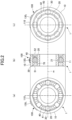
- FIG. 2 is a diagram illustrating an example of the rolling bearing according to the first embodiment.
- FIG. 2 (a) is a front view of the rolling bearing
- FIG. 2 (b) is a cross-sectional view of the rolling bearing
- FIG. 2 (c) is a back view of the rolling bearing.
- a rolling bearing 1 includes an outer ring 10, an inner ring 20, multiple rolling elements 30, a holder 40, seals 51 and 52, and a strain gauge 100.
- FIG. 2 (a) and FIG. 2 (c) illustration of seals 51 and 52 are omitted for the sake of convenience.
- the outer ring 10 has a cylindrical structure of which a central axis is a rotation axis m.
- the inner ring 20 has a cylindrical structure that is disposed coaxially with the outer ring 10 and that is provided on an inner peripheral side of the outer ring 10.
- Each of the rolling elements 30 is a sphere disposed in a race 70 that is formed between the outer ring 10 and the inner ring 20.
- a lubricant (not illustrated) such as grease is applied to the race 70.
- the seals 51 and 52 protrude from the inner peripheral surface of the outer ring 10 toward the inner ring 20 to isolate the race 70 from the outside.
- a recess 11 of which a cross-sectional shape is an arc shape is formed in a circumferential direction of the outer ring 10.
- a recess 21 of which a cross-sectional shape is an arc shape is formed in a circumferential direction of the inner ring 20 and at an outer peripheral surface of the inner ring 20.
- the rolling elements 30 are guided in the circumferential direction by the recesses 11 and 21.
- the holder 40 is disposed in the race 70, and holds the rolling elements 30.
- the holder 40 is an annular portion that is disposed coaxially with the rotation axis m.
- One side of the holder 40 in a direction of the rotation axis m includes recesses 41 for accommodating the respective rolling elements 30, and the other side of the holder 40 includes a back portion 42 that is continuously provided in the circumferential direction of the annular portion.
- FIG. 3 is an enlarged view of an example of a proximate portion of the strain gauge in FIG. 1 .
- the strain gauge 100 illustrated in FIGS. 1 to 3 is a sensor that detects strain in the outer ring 10 or the inner ring 20.
- the strain gauge 100 includes three or more detector elements.
- the strain gauge 100 is a resistive strain gauge that includes one or more resistors used as detector elements.
- the strain gauge 100 includes a first resistor 130 1 , a second resistor 130 2 , and a third resistor 130 3 , which serve as sensitive portions, on a substrate 110.
- the strain gauge 100 is disposed on the outer peripheral surface of the outer ring 10, and detects the strain in the outer ring 10 as changes in a resistance value of the first resistor 130 1 , the second resistor 130 2 , and the third resistor 130 3 .
- the first resistor 130 1 , the second resistor 130 2 , and the third resistor 130 3 are arranged such that a longitudinal direction (grid direction described below) of each of the resistors refers to a circumferential direction of the outer ring 10.
- the outer ring 10 is more likely to expand and contract in the circumferential direction than in the direction of the rotation axis m.
- the first resistor 130 1 , the second resistor 130 2 , and the third resistor 130 3 are each arranged such that the longitudinal direction of the resistor refers to the circumferential direction of the outer ring 10.
- CL is an imaginary line that divides the outer peripheral surface of the outer ring 10 into two portions in the circumferential direction, and CL indicates a centerline of the outer peripheral surface of the outer ring 10.
- the first resistor 130 1 is disposed on the centerline CL.
- the first resistor 130 1 may be disposed, for example, such that a middle portion in a grid-width direction (described below) coincides with the centerline CL.
- the first resistor 130 1 , the second resistor 130 2 , and the third resistor 130 3 differ from one another in a location in the circumferential direction and a location in the direction of the rotation axis m.
- the second resistor 130 2 is disposed on one side of the first resistor 130 1 in the circumferential direction and on one side of the centerline CL in the direction of the rotation axis m.
- the third resistor 130 3 is disposed on the other side of the first resistor 130 1 in the circumferential direction and on the other side of the centerline CL in the direction of the rotation axis m.
- the location of each resistor refers to a position of the center of gravity of a region (hereinafter referred to as a resistor formation region) in which resistors on the substrate 110 are formed, in a plan view.
- the second resistor 130 2 and the third resistor 130 3 are arranged to face each other in a direction oblique to the centerline CL such that the first resistor 130 1 is interposed between the second resistor 130 2 and the third resistor 130 3 .
- a case where the second resistor 1302 and the third resistor 130 3 are disposed to face each other such that the first resistor 130 1 is interposed between the second resistor 130 2 and the third resistor 130 3 means that a straight line, connecting a center of gravity of a resistor formation region of the second resistor 1302 and a center of gravity of a resistor formation region of the third resistor 1303, passes through any portion of the first resistor 130 1 in a plan view.
- a distance between the first resistor 130 1 and the second resistor 130 2 in the circumferential direction of the outer ring 10 is equal to a distance between the first resistor 130 1 and the third resistor 130 3 in the circumferential direction of the outer ring 10, for example.
- a distance between the first resistor 130 1 and the second resistor 130 2 in the direction of the rotation axis m is equal to a distance between the first resistor 130 1 and the third resistor 130 3 in the direction of the rotation axis m, for example.
- a distance between resistors refers to a distance between centers of gravity of resistor formation regions for respective resistors, in a plan view.
- the first resistor 130 1 , the second resistor 130 2 , and the third resistor 130 3 are arranged as illustrated in FIG. 3 .
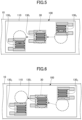
- changes in the output of the rolling elements 30 in the circumferential direction and changes in the output of the rolling elements 30 in the direction of the rotation axis m, in one cycle, can be detected.
- the trajectory of each rolling element 30 during rotation can be detected.
- the output of the second resistor 130 1 and the third resistor 130 3 is smaller than the output of the first resistor 130 1 .
- the trajectory of the rolling element 30 during rotation can be detected using a ratio of the output of the second resistor 130 2 and the third resistor 130 to the output of the first resistor 130 1 .
- the output of the second resistor 130 2 and the third resistor 130 3 is smaller than the output of the first resistor 130 1 , in comparison to the trajectory in FIG. 4 .
- both the trajectories in FIGS. 4 and 5 can be distinguished.
- the output of the first resistor 130 1 is the same as that obtained in the case of FIGS. 4 and 5 , while the output of the second resistor 130 2 and the third resistor 130 3 is approximately zero.
- a trajectory can be detected to be inclined in a direction opposite the direction of the trajectory obtained in FIG. 4 .
- changes in the trajectory of a given rolling element 30 can be identified.
- the trajectory of the rolling element 30 during rotation can be detected based on the output of the strain gauge 100, and thus a lifetime of the rolling bearing 1 can be predicted in consideration of the trajectory of the rolling element 30, the number of rotations and a preload of the rolling element 30. That is, a state of the rolling element 30 during rotation can be accurately identified based on the output of the strain gauge 100, and thus the lifetime can be predicted with higher accuracy. Further, the remaining lifetime can be diagnosed for various products that use the rolling bearing 1. In particular, when a Cr composite film described below is used for each resistor, the Cr composite film has a gauge factor of 10 or more and high sensitivity, thereby allowing for detection of a small displacement. Therefore, the trajectory of the rolling element 30 can be detected with high accuracy.
- resistors 130 When it is not necessary to distinguish the first resistor 130 1 , the second resistor 130 2 , and the third resistor 130 3 from one another, these resistors may be collectively referred to as resistors 130.
- FIG. 7 is a plan view of a proximate portion of one resistor of the strain gauge according to the first embodiment.
- FIG. 8 is a cross-sectional view of the proximate portion of one resistor of the strain gauge according to the first embodiment, and illustrates the cross section along the line A-A in FIG. 7 .
- the strain gauge 100 includes three sets each of which includes the resistor 130, lines 140, electrodes 150, and the cover layer 160, and these sets are disposed on one substrate 110.
- the strain gauge 100 includes three sets each of which includes the resistor 130, lines 140, electrodes 150, and the cover layer 160, and these sets are disposed on one substrate 110.
- FIG. 3 , 7, and 8 the strain gauge 100 includes three sets each of which includes the resistor 130, lines 140, electrodes 150, and the cover layer 160, and these sets are disposed on one substrate 110.
- three strain gauges each of which has one set in which the resistor 130, lines 140, electrodes 150, and the cover layer 160 are situated on one substrate 110 may be disposed on the outer peripheral surface of the outer ring 10.
- FIG. 7 only the outer edge of the cover layer 160 is expressed by a broken line for convenience.
- the cover layer 160 may be provided as necessary.
- the side of the substrate 110 where the resistors 130 are provided is referred to as an upper side or one side, and the side of the substrate 101 where the resistors 130 are not provided is referred to as a lower side or the other side.
- the surface on the side where the resistors 130 are provided is referred to as one surface or an upper surface, and the surface on the side where the resistors 130 are not provided is referred to as the other surface or a lower surface.
- the strain gauge 100 can be used in a state of being upside down, or can be disposed at any angle.
- a plan view means that an object is viewed from a direction normal to an upper surface 110a of the substrate 110, and a planar shape refers to a shape of an object when viewed from the direction normal to the upper surface 110a of the substrate 110.
- the substrate 110 is a member that is a base layer for forming the resistors 130 or the like, and is flexible.
- the thickness of the substrate 110 is not particularly restricted, and can be appropriately selected for any purpose. For example, such a thickness can be approximately from 5 um to 500 um. In particular, when the thickness of the substrate 110 is from 5 um to 200 ⁇ m, it is preferable in terms of strain transfer from a flexure element surface that is bonded to a lower surface of the substrate 110 via an adhesive layer or the like, and dimensional stability with respect to environment, and when the thickness is 10 um or more, it is further preferable in terms of insulation.
- the substrate 110 can be formed of an insulating resin film such as a polyimide (PI) resin, an epoxy resin, a polyether ether ketone (PEEK) resin, a polyethylene naphthalate (PEN) resin, a polyethylene terephthalate (PET) resin, a polyphenylene sulfide (PPS) resin, a liquid crystal polymer (LCP), or a polyolefin resin.
- PI polyimide
- PEEK polyether ether ketone
- PEN polyethylene naphthalate
- PET polyethylene terephthalate
- PPS polyphenylene sulfide
- LCP liquid crystal polymer
- the "formed of an insulating resin film” is not intended to preclude the substrate 110 from containing fillers, impurities, or the like in the insulating resin film.
- the substrate 110 may be formed, for example, of an insulating resin film containing fillers such as silica or alumina.
- Examples of the material of the substrate 110 other than the resin include crystal materials such as SiO 2 , ZrO 2 (including YSZ), Si, Si 2 N 3 , Al 2 O 3 (including sapphire), ZnO, and perovskite-based ceramics (CaTiO 3 , BaTiOs), and the examples further include amorphous glass or the like.
- a metal such as aluminum, an aluminum alloy (duralumin), or titanium may be used as the material of the substrate 110. In this case, for example, an insulating film is formed on the substrate 110 made of the metal.
- the resistor 130 is a thin film that is formed in a predetermined pattern and on the substrate 110.
- the resistor 130 is a sensitive portion where the resistance varies in accordance with strain.
- the resistor 130 may be formed directly on the upper surface 110a of the substrate 110, or may be formed above the upper surface 110a of the substrate 110 via one or more other layers. In FIG. 7 , for the sake of convenience, the resistor 130 is illustrated in a dense crepe pattern.
- the resistor 130 has a structure in which multiple elongated portions, of which longitudinal directions are the same direction (direction defined by the line A-A in FIG. 7 (circumferential direction)), are arranged at predetermined intervals, and in which ends of adjacent elongated portions are alternately coupled to each other, so that the resistor 130 extends with a back-and-forth zigzagging pattern as a whole.
- the longitudinal direction of the elongated portions refers to the grid direction
- a direction perpendicular to the grid direction refers to the grid-width direction (direction perpendicular to the line A-A (direction of the rotation axis m) in FIG. 7 ).
- one end of the elongated portion in the longitudinal direction is bent in the grid-width direction to form a corresponding end among an end 130e 1 and an end 130e 2 of the resistor 130 in the grid-width direction.
- the ends 130e 1 and 130e 2 of the resistor 130 in the grid-width direction are electrically coupled to the electrodes 150 via the lines 140, respectively.
- the lines 140 electrically connect the ends 130e 1 and 130e 2 of the resistor 130 in the grid-width direction to the electrodes 150, respectively.
- the resistor 130 can be each formed, for example, of material including Cr (chromium), material including Ni (nickel), or material including both of Cr and Ni.
- the resistor 130 can be formed of material including at least one of Cr or Ni.
- An example of the material including Cr includes a Cr composite film.
- An example of the material including Ni includes Cu-Ni (copper nickel).
- An example of the material including both of Cr and Ni includes Ni-Cr (nickel chromium).
- the Cr composite film is a composite film of Cr, CrN, and Cr 2 N, and the like.
- the Cr composite film may include incidental impurities such as chromium oxide.
- the thickness of the resistor 130 is not particularly restricted, and can be appropriately selected for any purpose.
- the thickness can be, for example, approximately from 0.05 um to 2 um.
- the thickness of the resistor 130 is 0.1 um or more, it is preferable in terms of increases in crystallinity (e.g., crystallinity of ⁇ -Cr) of a crystal that constitutes the resistor 130.
- the thickness of the resistor 130 is 1 um or less, it is further preferable in terms of reductions in cracks of a given film caused by internal stress of the film that constitutes the resistor 130, or reductions in warp in the substrate 110.
- the width of the resistor 130 is optimized based on required specifications of a resistance value and lateral sensitivity and the like, and the resulting width can be approximately from 10 um to 100 um in consideration of addressing disconnections.
- the resistor 130 is the Cr composite film
- ⁇ -Cr alpha-chromium
- stability of gauge characteristics can be increased.
- the gauge factor of the strain gauge 100 can be 10 or more
- a gauge factor temperature coefficient TCS and temperature coefficient of resistance TCR can be each in the range of -1,000 ppm/°C to +1,000 ppm/°C.
- a main component means that a target substance is at 50% by weight or more of total substances that constitute the resistor.
- the resistor 130 preferably includes ⁇ -Cr at 80% by weight or more, or more preferably at 90% by weight or more, from the viewpoint of increasing the gauge characteristics.
- ⁇ -Cr is Cr having a bcc structure (body-centered cubic structure).
- CrN and Cr 2 N included in the Cr composite film are preferably at 20% by weight or less.
- CrN and Cr 2 N included in the Cr composite film are at 20% by weight or less, reductions in the gauge factor can be suppressed.
- a percentage of Cr 2 N in the CrN and Cr 2 N is preferably greater than or equal to 80% and less than 90%, and more preferably greater than or equal to 90% and less than 95%.
- TCR negative TCR
- Cr 2 N having a semiconductor characteristic Further, with reductions in making of ceramics, brittle fracture is reduced.
- the lines 140 are formed on the substrate 110, and are electrically coupled to the resistor 130 and the electrodes 150.
- Each line 140 includes a first metal layer 141 and a second metal layer 142 that is laminated on the upper surface of the first metal layer 141.
- the linear shape of the line 140 is not restricted, and the line 140 can have any pattern.
- the line 140 can have any width and length. In FIG. 7 , for the sake of convenience, the line 140 and the electrodes 150 are each illustrated in a sparse crepe pattern, compared to the resistor 130.
- Each electrode 150 is formed on the substrate 110, and is electrically coupled to the resistor 130 through the line 140.
- the electrode 150 is wider than the line 140 to have an approximately rectangular shape.
- the electrodes 150 are a pair of electrodes through which changes in the resistance value of the resistor 130 in accordance with strain are externally output. For example, lead wires for external connection are bonded to the electrodes.
- the electrodes 150 include a pair of first metal layers 151, and include second metal layers 152 that are respectively laminated on upper surfaces of the first metal layers 151 in the pair.
- the first metal layer 151 is electrically coupled, at respective ends, to ends 130e 1 and 130e 2 of the resistor 130 via the first metal layer 141 of the line 140.
- the first metal layer 151 is formed to have an approximately rectangular shape in a plan view.
- the first metal layer 151 may be formed to have the same width as that of the line 140.
- the resistor 130, the first metal layer 141, and the first metal layer 151 are expressed by different numerals for the sake of convenience, these components can be integrally formed of the same material in the same process. With this approach, for the resistor 130, the first metal layer 141, and the first metal layer 151, these thicknesses are approximately identical. Further, the second metal layer 142 and the second metal layer 152 are expressed by different numerals for the sake of convenience, but these layers can be integrally formed of the same material in the same process. With this approach, for the second metal layer 142 and the second metal layer 152, the thicknesses are approximately identical.
- the second metal layers 142 and 152 are formed of a material having a resistance lower than that of the resistor 130 (the first metal layers 141 and 151).
- the material of the second metal layers 142 and 152 is not particularly restricted, and may be appropriately selected for any purpose, so long as the material has a lower resistance than the resistor 130.
- examples of the material of the second metal layers 142 and 152 include Cu, Ni, Al, Ag, Au, Pt, or the like; an alloy of any metals of these metals; a compound of any of these metals; or a laminated film that is obtained by appropriately laminating any metals of these metals, alloys, and compounds.
- the thickness of each of the second metal layers 142 and 152 is not particularly restricted, and can be appropriately selected for any purpose.
- the thickness of each of the second metal layers 142 and 152 can be approximately 3 um to 5 ⁇ m.
- the second metal layers 142 and 152 may be respectively formed on portions of the upper surfaces of the first metal layers 141 and 151, or may be respectively formed on the entire upper surfaces of the first metal layers 141 and 151. Any other metal layer(s) may be further laminated on the upper surface of the second metal layer 152.
- the second metal layer 152 may be a copper layer, and a gold layer may be laminated on the upper surface of the copper layer.
- the second metal layer 152 may be a copper layer, and a palladium layer and a gold layer may be sequentially laminated on and above the upper surface of the copper layer.
- the line 140 has a structure in which the second metal layer 142 is laminated on the first metal layer 141 that is made of the same material as the resistor 130. With this arrangement, the line 140 has a lower resistance than the resistor 130, and thus the line 140 can be prevented from functioning as a resistor. As a result, accuracy in detecting the strain by the resistor 130 can be increased.
- a substantial sensitive portion of the strain gauge 100 can be limited to a local region where the resistor 130 is formed. In this arrangement, accuracy in detecting the strain by the resistor 130 can be increased.
- a pattern for drawn lines 140 and locations of the electrodes 150 can be set as appropriate.
- the electrodes 150 coupled to respective resistors may be aligned to be situated at respective predetermined locations.
- the cover layer 160 is formed on and above the substrate 110 such that the resistor 130 and the lines 140 are coated and the electrodes 150 are exposed. A portion of each line 140 may be exposed from the cover layer 160.
- the cover layer 160 may be provided to cover all portions except for the electrodes 150.
- the cover layer 160 can be formed of an insulating resin such as a PI resin, an epoxy resin, a PEEK resin, a PEN resin, a PET resin, or a PPS resin, a composite resin (e.g., a silicone resin or a polyolefin resin).
- the cover layer 160 may contain fillers or pigments.
- the thickness of the cover layer 160 is not particularly restricted and can be appropriately selected for any purpose. For example, the thickness can be approximately from 2 um to 30 ⁇ m.
- the substrate 110 is fist prepared, and then a metal layer (hereinafter referred to as a metal layer A for the sake of convenience) is formed on the upper surface 110a of the substrate 110. Finally, the metal layer A is patterned to become a layer that forms the resistor 130, the first metal layer 141, and the first metal layer 151. The material and the thickness of the metal layer A are set as in the material and the thickness for the resistor 130, the first metal layer 141, and the first metal layer 151.
- the metal layer A can be formed, for example, by magnetron sputtering that uses a raw material capable of forming the metal layer A as a target.
- the metal layer A may be formed by reactive sputtering, vapor deposition, arc ion plating, pulse laser deposition, or the like, instead of using the magnetron sputtering.
- a functional layer having a predetermined film thickness is vacuum-deposited as a base layer on the upper surface 110a of the substrate 110, for example, by conventional sputtering, before the metal layer A is formed.
- the functional layer refers to a layer that has a function of promoting crystal growth of the metal layer A (resistor 130) that is at least an upper layer.
- the functional layer preferably further has a function of preventing oxidation of the resistors caused by oxygen and moisture included in the substrate 110, as well as a function of improving adhesion between the substrate 110 and the metal layer A.
- the functional layer may further have any other functions.
- the insulating resin film that constitutes the substrate 110 contains oxygen and moisture.
- the metal layer A includes Cr
- the material of the functional layer is not particularly restricted as long as it is material having a function of promoting crystal growth of the metal layer A (resistor 130) that is at least an upper layer.
- Such material can be appropriately selected for any purpose, and includes one or more types of metals selected from the group consisting of, for example, Cr (chromium), Ti (titanium), V (vanadium), Nb (niobium), Ta (tantalum), Ni (nickel), Y (yttrium), Zr (zirconium), Hf (hafnium), Si (silicon), C (carbon), Zn (zinc), Cu (copper), Bi (bismuth), Fe (iron), Mo (molybdenum), W (tungsten), Ru (ruthenium), Rh (rhodium), Re (rhenium), Os (osmium), Ir (iridium), Pt (platinum), Pd (palladium), Ag (silver), Au (gold), Co (cobalt), Mn (manganese
- Examples of the above alloy include FeCr, TiAl, FeNi, NiCr, CrCu, and the like.
- Examples of the above compound include TiN, TaN, Si 3 N 4 , TiO 2 , Ta 2 O 5 , SiO 2 , and the like.
- the film thickness of the functional layer is preferably 1/20 or less of the film thickness of the resistor.
- the thickness is in such a range, crystal growth of ⁇ -Cr can be promoted. Also, a portion of the current through the resistor can be prevented from flowing through the functional layer to reduce detection sensitivity of the strain.
- the film thickness of the functional layer is more preferably 1/50 or less of the film thickness of the resistor.
- the thickness is in such a range, crystal growth of ⁇ -Cr can be promoted, and a portion of the current through the resistor can be prevented from flowing through the functional layer to further prevent the detection sensitivity of strain from being reduced.
- the film thickness of the functional layer is more preferably 1/100 or less of the film thickness of the resistor.
- the thickness is in such a range, reductions in the detection sensitivity of the strain due to a portion of the current through the resistor flowing through the functional layer can be further prevented.
- the film thickness of the functional layer is preferably from 1 nm to 1 um.
- the thickness is in such a range, the crystal growth of ⁇ -Cr can be promoted, and the film can be easily formed without causing any cracks in the functional layer.
- the film thickness of the functional layer is more preferably from 1 nm to 0.8 um.
- the thickness is in such a range, the crystal growth of ⁇ -Cr can be promoted, and the film can be more easily formed without causing any cracks in the functional layer.
- the film thickness of the functional layer is more preferably from 1 nm to 0.5 um.
- the thickness is in such a range, the crystal growth of ⁇ -Cr can be promoted, and the functional layer can be more easily formed without causing any cracks in the functional layer.
- a planar shape of the functional layer is patterned to be approximately as same as a planar shape of the resistor illustrated in FIG. 7 , for example.
- the planar shape of the functional layer is not limited to a case where it is approximately the same as the planar shape of the resistor.
- the functional layer may not be patterned to have the same shape as the planar shape of the resistor.
- the functional layer may be formed in a solid state in at least a region where the resistor is formed.
- the functional layer may be formed in a solid manner on the entire upper surface of the substrate 110.
- the functional layer when the functional layer is formed of the insulating material, the functional layer is formed relatively thick to be greater than or equal to 50 nm and less than or equal to 1 um, and is formed in the solid manner. Thus, the thickness and the surface area of the functional layer are increased. Therefore, heat generated by the resistor can be dissipated toward the substrate 110. As a result, in the strain gauge 100, reductions in measurement accuracy due to the self-heating of the resistor can be suppressed.
- the functional layer can be vacuum-deposited, for example, by conventional sputtering in which a raw material capable of forming the functional layer is used as a target and an Ar (argon) gas is introduced into a chamber.
- Ar argon
- the functional layer is deposited while the upper surface 110a of the substrate 110 is etched with Ar. With this approach, the effect of improving adhesion can be obtained by minimizing an amount of the functional layer that is deposited.
- the functional layer may be vacuum-deposited by another method.
- a method may be used in which the upper surface 110a of the substrate 110 is activated by plasma treatment that uses Ar or the like before the formation of the functional layer to obtain the effect of improving adhesion, and in which then the functional layer is vacuum-deposited by magnetron sputtering.
- a combination of the material of the functional layer and the material of the metal layer A is not particularly restricted, and can be appropriately selected for any purpose.
- Ti is used as the functional layer
- a Cr composite film that is formed with ⁇ -Cr (alpha chromium) as the main component can be deposited as the metal layer A.
- the metal layer A can be deposited by magnetron sputtering in which a raw material capable of forming the Cr composite film is used as a target, and in which Ar gas is introduced into a chamber.
- the metal layer A may be deposited by reactive sputtering in which pure Cr is used as a target, and in which an appropriate amount of nitrogen gas, together with an Ar gas, is introduced into the chamber.
- a percentage of CrN and Cr 2 N contained in the Cr composite film, and a percentage of Cr 2 N in CrN and Cr 2 N can be adjusted by changing an introduced amount or pressure (partial pressure of nitrogen gas), or by providing a heating step to adjust a heating temperature.
- a growth face of the Cr composite film is defined by the functional layer made of Ti, and thus the Cr composite film containing ⁇ -Cr as the main component that has a stable crystal structure can be deposited.
- Ti constituting the functional layer diffuses into the Cr composite film, thereby improving the gauge characteristic.
- the gauge factor of the strain gauge 100 can be set to 10 or more, and each of the gauge factor temperature coefficient TCS and the resistance temperature coefficient of resistance TCR can be set to be within the range of -1,000 ppm/°C to +1,000 ppm/°C.
- the Cr composite film may contain Ti or TiN (titanium nitride).
- the functional layer made of Ti has all functions of a function of promoting crystal growth of the metal layer A, a function of preventing oxidation of the metal layer A due to oxygen or moisture that is contained in the substrate 110, and a function of improving adhesion between the substrate 110 and the metal layer A.
- the same functions as described above are implemented in a case where instead of Ti, Ta, Si, Al, or Fe is used as the functional layer.
- the functional layer under the metal layer A by providing the functional layer under the metal layer A, the crystal growth of the metal layer A can be promoted, and the metal layer A having the stable crystal phase can be produced.
- stability of the gauge characteristic can be improved in the strain gauge 100.
- a given material that constitutes the functional layer diffuses into the metal layer A, and thus the gauge characteristic of the strain gauge 100 can be improved.
- the second metal layer 142 and the second metal layer 152 are formed on the upper surface of the metal layer A.
- the second metal layer 142 and the second metal layer 152 can be formed, for example, by photolithography.
- a seed layer is first formed, for example, by sputtering or electroless plating so as to cover the upper surface of the metal layer A.
- a photosensitive resist is formed on the entire upper surface of the seed layer, and the photosensitive resist is exposed and developed to form an opening through which a region where the second metal layer 142 and the second metal layer 152 are to be exposed.
- a pattern of the second metal layer 142 can be formed to have any shape, by adjusting the shape of the opening of the resist.
- the resist for example, a dry film resist or the like can be used.
- the second metal layer 142 and the second metal layer 152 are formed on the seed layer exposed in the opening.
- the electrolytic plating is suitable in that high tact is obtained and an electrolytic plating layer with low stress can be formed as each of the second metal layer 142 and the second metal layer 152.
- the second metal layer 142 and the second metal layer 152 may be formed by electroless plating.
- the resist is removed.
- the resist can be removed, for example, by immersing the substrate in a solution capable of dissolving the material of the resist.
- a photosensitive resist is formed on the entire upper surface of the seed layer, and the photosensitive resist is exposed and developed to be patterned to have the same planar shape as the resistor 130, the lines 140, and the electrodes 150 in FIG. 7 .
- the resist for example, a dry film resist or the like can be used.
- the resist is used as an etching mask to remove the metal layer A and the seed layer that are exposed from the resist.
- the resistor 130, the lines 140, and the electrodes 150 as illustrated in the planar shape in FIG. 7 are formed.
- An unnecessary portion of the metal layer A and the seed layer can be removed, for example, by wet etching.
- the functional layer is formed under the metal layer A, the functional layer is patterned to have the planar shape illustrated in FIG. 7 by etching, as in the resistor 130, the line 140, and the electrodes 150.
- the seed layer is formed on the resistor 130, the first metal layer 141, and the first metal layer 151.
- the second metal layer 142 and the second metal layer 152 are used as etching masks to remove an unnecessary seed layer that is exposed from the second metal layer 142 and the second metal layer 152, thereby forming the second metal layer 142 and the second metal layer 152.
- the seed layer that is immediately below the second metal layer 142 and the second metal layer 152 remains.
- an unnecessary seed layer can be removed by wet etching that uses an etchant with which the seed layer is etched but the functional layer, the resistor 130, the lines 140, and the electrodes 150 are not etched.
- the cover layer 160 with which the resistor 130 and the lines 140 are coated and through which the electrodes 150 are exposed is provided on and above the upper surface 110a of the substrate 110.
- the cover layer 160 can be formed, for example, by laminating a semi-cured insulating film on the upper surface 110a of the substrate 110 so as to cover the resistor 130 and the line 140 and expose the electrodes 150, and by heating and curing the insulating film.
- the cover layer 160 may be formed by applying a liquid or paste heat-curable insulating material to the upper surface 110a of the substrate 110 so as to cover the resistor 130 and the lines 140 and to expose the electrodes 150, and by heating and curing the insulating material.
- FIG. 9 is an enlarged view of the proximate portion of the strain gauge in the first modification of the first embodiment.
- a strain gauge 100A differs from the strain gauge 100 in that the strain gauge 100A includes a fourth resistor 130 4 and a fifth resistor 130 5 .
- the fourth resistor 130 4 and the fifth resistor 130 5 are each arranged such that a grid direction of the resistor refers to the circumferential direction of the outer ring 10.
- the fourth resistor 130 4 is disposed at the same location in the circumferential direction as the second resistor 130 2 , but is disposed at a different location from the second resistor 130 2 in the direction of the rotation axis m.
- the fifth resistor 130 5 is disposed at the same location in the circumferential direction as the third resistor 130 3 , but is disposed at a different location from the third resistor 130 3 in the direction of the rotation axis m. That is, the fourth resistor 130 4 and the fifth resistor 130 5 are at different locations in both the circumferential direction and the direction of the rotation axis m.
- the fourth resistor 130 4 and the fifth resistor 130 5 are arranged to face each other such that the first resistor 130 1 is interposed between the fourth resistor 130 4 and the fifth resistor 130 5 in a direction oblique to the centerline CL.
- the strain gauge includes three or more resistors, and further the three or more resistors include at least two resistors that are situated at different locations in the circumferential direction of the outer ring and in the direction of the rotation axis of the outer ring.
- the trajectory of the rolling element 30 can be detected. Examples of the configuration will be described below, but the examples illustrated below are by no means a limitation.
- FIG. 10 is an enlarged view (first part) of the proximate portion of the strain gauge in the second modification of the first embodiment.
- a strain gauge 100B includes a sixth resistor 130 6 , a seventh resistor 130 7 , an eighth resistor 130 8 , and a ninth resistor 130 9 that are disposed on the substrate 110.
- the sixth resistor 130 6 , the seventh resistor 130 7 , the eighth resistor 130 8 , and the ninth resistor 130 9 are each arranged such that the grid direction of the resistor refers to the circumferential direction of the outer ring 10.
- the sixth resistor 130 6 and the seventh resistor 130 7 are disposed on one side of the centerline CL.
- the eighth resistor 130 8 and the ninth resistor 130 9 are disposed on the other side of the centerline CL.
- the sixth resistor 130 6 and the seventh resistor 130 7 are situated at different locations in the circumferential direction, and the eighth resistor 130 8 and the ninth resistor 130 9 are situated at different locations in the circumferential direction.
- the sixth resistor 130 6 and the eighth resistor 130 8 are situated at the same location in the circumferential direction, and the seventh resistor 130 7 and the ninth resistor 130 9 are situated at the same location in the circumferential direction.
- the trajectory of the rolling element 30 illustrated in FIG. 5 can be detected.
- the trajectory of the rolling element 30 illustrated in FIG. 4 can be detected.
- the output of the sixth resistor 130 6 is smaller than the output of the eighth resistor 130 8
- the output of the ninth resistor 130 9 is smaller than the output of the seventh resistor 130 7
- the trajectory of the rolling element 30 illustrated in FIG. 6 can be detected.
- the output from each resistor can be increased in a case where the trajectory of the rolling element 30 illustrated in FIG. 5 is obtained.
- FIG. 11 is an enlarged view (second part) of the proximate portion of the strain gauge in the second modification of the first embodiment.
- a strain gauge 100C differs from the strain gauge 100B in that the strain gauge 100C includes a tenth resistor 130 10 and an eleventh resistor 130 11 .
- the tenth resistor 130 10 and the eleventh resistor 130 11 are each arranged such that the grid direction of the resistor refers to the circumferential direction of the outer ring 10.
- the tenth resistor 130 10 is disposed on one side of the centerline CL, and the eleventh resistor 130 11 is disposed on the other side of the centerline CL.
- the tenth resistor 130 10 and the eleventh resistor 130 11 are situated at the same location in the circumferential direction.
- the tenth resistor 130 10 and the sixth resistor 130 6 are arranged in parallel to the centerline CL to face each other such that the seventh resistor 130 7 is interposed between the tenth resistor 130 10 and the sixth resistor 130 6 .
- the eleventh resistor 130 11 and the eighth resistor 130 8 are arranged in parallel to the centerline CL to face each other such that the ninth resistor 130 9 is interposed between the eleventh resistor 130 11 and the eighth resistor 130 8 .
- FIG. 12 is an enlarged view (third part) of the proximate portion of the strain gauge in the second modification of the first embodiment.
- a strain gauge 100D includes a twelfth resistor 130 12 , a thirteenth resistor 130 13 , a fourteenth resistor 130 14 , and a fifteenth resistor 130 15 that are arranged on the substrate 110.
- the twelfth resistor 130 12 , the thirteenth resistor 130 13 , the fourteenth resistor 130 14 , and the fifteenth resistor 130 15 are each arranged such that the grid direction of the resistor refers to the circumferential direction of the outer ring 10.
- the twelfth resistor 130 12 and the thirteenth resistor 130 13 are disposed on the centerline CL.
- the twelfth resistor 130 12 and the thirteenth resistor 130 13 may be each disposed, for example, such that a middle portion in the grid-width direction coincides with the centerline CL.
- the fourteenth resistor 130 14 is disposed between the twelfth resistor 130 12 and the thirteenth resistor 130 13 in the circumferential direction, and the fourteenth resistor 130 14 is disposed on one side of the centerline CL.
- the fifteenth resistor 130 15 is located between the twelfth resistor 130 12 and the thirteenth resistor 130 13 in the circumferential direction, and the fifteenth resistor 130 15 is disposed on the other side of the centerline CL.
- the fourteenth resistor 130 14 and the fifteenth resistor 130 15 are situated at the same location in the circumferential direction.
- the trajectory of the rolling element 30 illustrated in FIG. 5 can be detected based on output levels of the twelfth resistor 130 12 and the thirteenth resistor 130 13 . Further, when either a case where outputs of the twelfth resistor 130 12 and the fifteenth resistor 130 15 have an approximate level, or a case where outputs of the thirteenth resistor 130 13 and the fourteenth resistor 130 14 have an approximate level occurs, the trajectory of the rolling element 30 illustrated in FIG. 4 can be detected.
- the example in which a given strain gauge is disposed on the outer peripheral surface of the outer ring to detect the strain in the outer ring is illustrated.
- the given strain gauge may be disposed on the inner peripheral surface of the inner ring to detect the strain in the inner ring.
- the trajectory of the rolling element 30 can be detected by arranging the resistors as illustrated in FIG. 3 or the like.
- the strain gauge 100 in the present disclosure is not limited to the resistive strain gauge.
- the strain gauge 100 may be a strain gauge that includes three or more detector elements that detect a magnetic change occurring in accordance with strain that is generated at the outer peripheral surface of the outer ring or the inner peripheral surface of the inner ring.
- the strain gauge 100 may be a strain gauge with detector elements that use a Villari effect (described below).
- the strain gauge 100 may be a strain gauge with detector elements each of which has a structure of a magnetic tunnel junction (described below).
- the strain gauge 100 with detector elements that use the Villari effect is described below.
- the strain gauge 100 with detector elements each of which has the structure of the magnetic tunnel junction is described below.
- FIG. 13 is a diagram illustrating an example of a detector element 300 included in the strain gauge 100 according to the second embodiment.
- (a) of FIG. 13 is a plan view of the detector element 300 when viewed from the upper surface (that is, a surface opposite an attachment surface) of the detector element in a case where that the detector element is attached to the substrate 110, as in the resistors 130 1 , 130 2 , and 130 3 in FIG. 1 .
- (b) of FIG. 13 is a cross-sectional view of the detector element 300, as illustrated in (a) of FIG. 13 , defined by a plane taken along the line ⁇ - ⁇ '.
- One or more lines for the detector element 300 are not illustrated in all parts of FIG. 13 .
- the detector element 300 may have a line for connecting a drive coil 320 described below and a power source, and may have a line for transmitting the current that is detected using a sensing coil 380.
- the detector element 300 includes the drive coil 320, the sensing coil 380, and a base layer 310.
- the sensing coil 380 is a coil in which the base layer 310 is used as a core material.
- the drive coil 320 is a coil in which the base layer 310 is used as a core material, and that is wound around the outer surface of the sensing coil.
- the drive coil 320 and the sensing coil 380 form a dual structure in which the drive coil 320 is located outside and the sensing coil 380 is located inside.
- an alternating magnetic field (described below) can be uniformly applied to the entire sensing coil 380. This improves the performance of the detector element 300.
- the drive coil 320 is a coil for generating a magnetic field. When an alternating current is supplied from the power source to the drive coil 320, the drive coil 320 generates an alternating magnetic field around the drive coil.
- the base layer 310 is formed by covering an approximately flat metal plate (base metal 370 described below) with an insulating layer (insulating layer 360 described below).
- the metal plate of the base layer 310 is a magnetic material in the detector element 300.
- the metal plate of the base layer 310 is magnetized by the alternating magnetic field that is generated through the drive coil 320.
- the sensing coil 380 is a coil for detecting the strength of magnetism in the base metal 370.
- the material of the drive coil 320 and the sensing coil 380 is desirably a conductive metal such as Cu, Ag, Al, and Au, and an alloy of any metals of these metals.
- the number of turns, and a size of an cross-sectional area, for each of the drive coil 320 and the sensing coil 380 may be appropriately designed in light of the detection sensitivity of the strain required for the detector element 300.
- the detector element 300 will be described in more detail with reference to the cross-sectional view in (b) of FIG. 13 .
- the layers 340 to 360 described below form a structure in which these layers are wound around the base metal 370 as the core material.
- given layers expressed by the same numeral are continuously connected to each other while surrounding the base metal 370.
- the detector element 300 has the structure in which the sensing coil 380 and the drive coil 320 are wound around the base layer 310.
- the base layer 310 has a structure in which the base metal 370 is covered with the insulating layer 360.
- the insulating layer 350 is formed to surround the insulating layer 360.
- the insulating layer 350 is a layer that includes the sensing coil 380, and is a layer in which each space between sensing coils 380 is filled with an insulating material.
- the insulating layer 340 is formed so as to surround the insulating layer 350.
- the insulating layer 340 is a layer with the drive coil 320, and is a layer in which each space between drive coils 320 is filled with an insulating material.
- the base metal 370 is preferably made of a soft magnetic material that includes an Fe-Si-Al alloy such as Sendust, or an Ni-Fe alloy such as Permalloy.
- the insulating layers 340, 350, and 360 are preferably dry films or cured resists such as photosensitive polyimide that do not affect the magnetic field.
- the attachment surface of the detector element 300 is attached to the substrate 110.
- the detector element 300 may be a detector element that has a flat plate shape or a thin film shape as a whole. When the detector element 300 has the flat plate shape or the thin film shape, the detector element can be more easily attached to the substrate 110.
- the detector element 300 includes the base metal 370 that is a magnetic element.
- the base metal 370 that is a magnetic element.
- the magnetic field is generated, and thus the base metal 370 is magnetized.
- the strain is transmitted to the substrate 110, and thus stress is applied to the base metal 370.
- a magnetic permeability of the base metal 370 changes in accordance with the stress, and thus the strength of magnetism changes.
- Such a phenomenon in which the magnetic permeability and the strength of magnetism in the magnetic material change due to the stress applied to the magnetic material is referred to as the "Villari effect.”
- an alternating current voltage corresponding to the strength of magnetism in the base metal 370 is induced in the sensing coil 380 that is a pick-up coil.
- the stress applied to the base metal 370 that is, a degree of strain in the substrate 110
- the grid direction of the detector element 300 refers to the ⁇ - ⁇ ' direction in (a) of FIG. 13 .
- the detector element 300 can detect the strain that is received by the substrate 110. That is, the detector element 300 functions as a detector element of the strain gauge 100.
- the strain gauge 100 includes three or more detector elements 300 as described above. At least two of the detector elements 300 are arranged at different locations in the circumferential direction of the outer ring 10 or the inner ring 20, and at least two of the detector elements 300 are arranged at different locations in the rotation axis direction. In this arrangement, according to the present embodiment, the rolling bearing 1 capable of detecting the trajectory of the rolling element during rotation can be provided.
- the detector elements 300 in the strain gauge 100 according to the present embodiment can be disposed at respective locations described in each of the first embodiment, the first modification of the first embodiment, and the second modifications of the first embodiment. That is, instead of the resistors 130 (resistors 130 1 to 130 15 ) according to the first embodiment, the detector elements 300 can be used. In this arrangement, each detector element 300 that provides the Villari effect can be used to detect the trajectory of the rolling element in the same manner as the case where the resistive strain gauge is used.
- the strain gauge 100 according to the present embodiment provides the same effects as those of the strain gauge 100 described in the first embodiment and the first and second modifications of the first embodiment.
- FIG. 14 is a diagram illustrating an example of a detector element 500 included in the strain gauge 100 according to the third embodiment.
- FIG. 15 is a diagram illustrating another example of the detector element according to the third embodiment.
- FIG. 16 is a diagram illustrating still another example of the detector element according to the third embodiment.
- (a) of each of FIGS. 14 to 16 is a perspective view of a corresponding detector element among detector elements 500, 600, and 700.
- (b) of each of FIGS. 14 to 16 is a plan view of the corresponding detector element among the detector elements 500, 600, and 700, when viewed from a negative z-axis direction, (c) of each of FIGS.
- each of the detector elements 500, 600, and 700 is a cross-sectional view of the corresponding detector element, among the detector elements 500, 600, and 700, taken in a plane parallel to a zy plane.
- the surface of each of the detector elements 500, 600, and 700 to be attached to the outer ring 10 or the inner ring 20 is a flat surface (surface parallel to an xy plane) that is situated on a lower side (in a negative z-axis direction).
- lines of the detector element are not illustrated.
- each of the detector elements 500, 600, and 700 may have one or more lines for coupling an upstream electrode 510 to a power source, and may include one or more lines for connecting a downstream electrode 520 and the power source, as described below.
- each of the detector elements 500, 600, and 700 includes the upstream electrode 510, the downstream electrode 520, magnetic films 530, and an insulating film 540.
- the insulating film 540 is interposed between the magnetic films 530 as illustrated in the figure.
- the magnetic films 530 and the insulating film 540 form a magnetic tunnel junction. That is, the detector element 500 has a structure in which electrodes are coupled to a structure of the magnetic tunnel junction.
- a positive z-axis direction is also referred to as an "upper side”
- a negative z-axis direction is also referred to as a "lower side.”
- a flexible substrate that is formed of a plastic film or the like may be further provided on the lower side of the upstream electrode 510 and/or the downstream electrode 520. The substrate may also serve as the substrate 110.
- the magnetic film 530 is a thin magnetic nanofilm.
- the insulating film 540 is a thin nanofilm of an insulator.
- the materials of the magnetic film 530 and the insulating film 540 are not particularly restricted as long as the structure of the magnetic tunnel junction can be formed.
- the magnetic film 530 cobalt-iron-boron or an alloy or the like containing a ferromagnetic material with 3d transition metal, such as Fe, Co, and Ni, and the above materials.
- the insulating film 540 silicon oxide, silicon nitride, aluminum oxide, magnesium oxide, or the like can be used.
- the upstream electrode 510 and the downstream electrode 520 are electrodes for applying a voltage to the structure of the magnetic tunnel junction.
- the current flows from the upstream electrode 510 to the downstream electrode 520.
- the voltage when the voltage is applied between the upstream electrode 510 and the downstream electrode 520, electrons flow from the upper magnetic film 530 into the lower magnetic film 530 through the insulating film 540. This is a phenomenon called "tunnelling," and the electric resistance obtained in a case where the electrons pass through the insulating film 540 is referred to as "tunnel resistance.”
- a junction of each electrode portion has a structure in which an end of the electrode is processed such that short pass for the current is not created through the structure of the magnetic tunnel junction.
- the detector element 500 When strain is applied to the detector element 500 through the substrate 110 or the like, a magnetic change occurs in the tunnel junction structure. More specifically, magnetization directions of the upper and lower magnetic films 530 do not match. When the magnetization directions of the upper and lower magnetic films 530 do not match, the tunnel resistance becomes large in comparison to a case where the magnetization directions are parallel to each other (tunnel magnetoresistance effect). With this arrangement, in the detector element 500 that has the above configuration, the current flowing between the electrodes decreases in accordance with the magnitude of the strain in the detector element 500 (more strictly, a portion of the magnetic tunnel junction). That is, the electrical resistance increases in accordance with an increasing magnitude of the strain. The detector element 500 can detect the strain based on a current magnitude with respect to an applied voltage. In this arrangement, by attaching the detector elements 500 to the outer ring 10 or the inner ring 20 in the rolling bearing 1, strain applied to the rolling bearing can be measured.
- the detector element having the structure of the magnetic tunnel junction is not limited to the detector element illustrated in the example of FIG. 14 .
- the detector elements 600 and 700 as illustrated in FIGS. 15 and 16 can be adopted.
- each of the detector element 600 illustrated in FIG. 15 and the detector element 700 illustrated in FIG. 16 has a configuration that includes the upstream electrode 510, the downstream electrode 520, the magnetic film 530, and the insulating film 540, and that provides a principle of detecting strain.
- the basic operation of the detector elements 600 and 700 is also the same as that of the detector element 500.
- the grid directions of the detector elements 500, 600, and 700 correspond to the y-axis directions (the positive y-axis direction and the negative y-axis direction) in FIGS.
- the detector element 600 has a structure in which the upper magnetic film 530 and the lower magnetic film 530 are partially connected to each other. That is, the structure of the magnetic tunnel junction is formed in only a partial region of the magnetic film 530, and a tunnel magnetoresistance effect occurs in the structure.
- the detector element 700 illustrated in FIG. 16 is attached to the substrate 110 via the substrate 710.
- design of the detector element may appropriately change according to the required size, durability, the magnitude of stress to be detected, and the like, as long as the principle described above is provided.
- Each of the detector elements 500, 600, and 700 may include approximately the same flat plate shape, such as a plate film shape as a whole. In this arrangement, the detector element 500 can be easily attached to the substrate 110.
- Each of the detector elements 500, 600, and 700 may have a structure for applying a weak magnetic field to a structural portion such as a drive coil of the magnetic tunnel junction. By applying the magnetic field to the structural portion of the magnetic tunnel junction, the above-described tunnel magnetoresistance effect can be measure more stably. Thus, strain can be detected stably.
- the "upstream electrode” and the “downstream electrode” in each of the detector elements 500, 600, and 700 are terms for the sake of convenience, and the direction in which the current flows may be reversed. That is, the detector elements 500, 600, and 700 illustrated in FIGS. 14 to 16 may be designed such that the current flows from the downstream electrode 520 to the upstream electrode 510.
- the strain gauge 100 includes three or more detector elements 500; three or more detector elements 600; or three or more detector elements 700 as described above.
- at least two detector elements 500 of the detector elements 500, at least two detector elements 600 of the detector elements 600, or at least two detector elements 700 of the detector elements 700 are disposed such that locations of the detector elements in the circumferential direction of the outer ring 10 or the inner ring 20 are different from each other, and such that locations of the detector elements in the direction of the rotation axis are different from each other.
- the rolling bearing 1 capable of detecting the trajectory of a given rolling element during rotation can be provided.
- the detector elements 500, 600, and 700 in the strain gauge 100 according to the present embodiment can be disposed at respective arrangement locations described in the first embodiment, the first modification of the first embodiment, and the second modifications of the first embodiment. That is, instead of a set of resistors 130 (resistors 130 1 to 130 15 ) according to the first embodiment, a set of detector elements 500, 600, or 700 can be used. In this arrangement, the detector elements 500, 600, and 700 that utilize the magnetic tunnel effect can be used to detect the trajectory of the rolling element, as in a case where the resistive strain gauge 100 is used.
- the strain gauge 100 according to the present embodiment provides the same effects as described in the strain gauge 100 according to the first embodiment and the first and second modifications of the first embodiment.
- a given strain gauge is disposed on the outer peripheral surface of the outer ring to detect the strain in the outer ring.
- the given strain gauge is disposed on the inner peripheral surface of the inner ring to detect the strain in the inner ring.
- the trajectory of the rolling element 30 can be detected by arranging the resistors as illustrated in FIG. 3 or the like.
Landscapes
- Engineering & Computer Science (AREA)
- General Engineering & Computer Science (AREA)
- Mechanical Engineering (AREA)
- Physics & Mathematics (AREA)
- General Physics & Mathematics (AREA)
- Chemical & Material Sciences (AREA)
- Analytical Chemistry (AREA)
- Measurement Of Length, Angles, Or The Like Using Electric Or Magnetic Means (AREA)
- Rolling Contact Bearings (AREA)
Abstract
Description
- The present invention relates to a rolling bearing.
- A rolling bearing is known as including an outer ring with a race on an inner peripheral side of the outer ring, an inner ring with a race on an outer peripheral side of the inner ring, rolling elements interposed between the race of the outer ring and the race of the inner ring, and strain gauges capable of being attached to the surface of the outer ring or the inner ring. The rolling bearing has two strain gauges that are attached along an axial direction of the outer ring (see
Patent Document 1, for example). - Patent Document 1:
Japanese Unexamined Patent Application Publication No. 2005-249594 - However, a conventional rolling bearing cannot detect a trajectory of the rolling element when rotating.
- In view of the situation described above, an object of the present invention is to provide a rolling bearing capable of detecting a trajectory of a rolling element when the rolling bearing rotates.
- A rolling bearing includes an outer ring having a predetermined rotation axis; an inner ring disposed coaxially with the outer ring, and situated on an inner peripheral side of the outer ring; multiple rolling elements disposed between the outer ring and the inner ring; and a strain gauge disposed on an outer peripheral surface of the outer ring or an inner peripheral surface of the inner ring. The strain gauge includes three or more detector elements that are disposed on the outer peripheral surface of the outer ring or the inner peripheral surface of the inner ring, and the three or more detector elements include at least two detector elements at different locations in a circumferential direction of the outer ring or the inner ring, the at least two detector elements being situated at different locations in a direction of the rotation axis.
- According to a disclosed technique, a rolling bearing capable of detecting a trajectory of a rolling element when the rolling bearing rotates can be provided.
-
- [
FIG. 1] FIG. 1 is a perspective view of an example of a rolling bearing according to a first embodiment. - [
FIG. 2] FIG. 2 is a diagram illustrating an example of the rolling bearing according to the first embodiment. - [
FIG. 3] FIG. 3 is an enlarged view of an example of a proximate portion of a strain gauge inFIG. 1 . - [
FIG. 4] FIG. 4 is a diagram (first part) for describing detection of a trajectory of a rolling element. - [
FIG. 5] FIG. 5 is a diagram (second part) for describing detection of the trajectory of the rolling element. - [
FIG. 6] FIG. 6 is a diagram (third part) for describing detection of the trajectory of the rolling element. - [
FIG. 7] FIG. 7 is a plan view of a proximate portion of one resistor in the strain gauge according to the first embodiment. - [
FIG. 8] FIG. 8 is a cross-sectional view of the proximate portion of one resistor in the strain gauge according to the first embodiment. - [
FIG. 9] FIG. 9 is an enlarged view of the proximate portion of the strain gauge in a first modification of the first embodiment. - [
FIG. 10] FIG. 10 is an enlarged view (first part) of the proximate portion of the strain gauge in a second modification of the first embodiment. - [
FIG. 11] FIG. 11 is an enlarged view (second part) of the proximate portion of the strain gauge in the second modification of the first embodiment. - [
FIG. 12] FIG. 12 is an enlarged view (third part) of the proximate portion of the strain gauge in the second modification of the first embodiment. - [
FIG. 13] FIG. 13 is a plan view and a cross-sectional view of an example of a detector element included in the strain gauge according to a second embodiment. - [
FIG. 14] FIG. 14 is a perspective view, a plan view, and a cross-sectional view of an example of the detector element included in the strain gauge according to a third embodiment. - [
FIG. 15] FIG. 15 is a perspective view, a plan view, and a cross-sectional view of another example of the detector element included in the strain gauge according to the third embodiment. - [
FIG. 16] FIG. 16 is a perspective view, a plan view, and a cross-sectional view of still another example of the detector element included in the strain gauge according to the third embodiment. - Embodiments for carrying out the invention are described below with reference to the drawings. In each drawing, the same components are indicated by the same numerals, and accordingly, duplicate description may be omitted.
-
FIG. 1 is a perspective view of an example of a rolling bearing according to a first embodiment.FIG. 2 is a diagram illustrating an example of the rolling bearing according to the first embodiment.FIG. 2 (a) is a front view of the rolling bearing,FIG. 2 (b) is a cross-sectional view of the rolling bearing, andFIG. 2 (c) is a back view of the rolling bearing. - Referring to
FIG. 1 andFIG. 2 , a rollingbearing 1 includes anouter ring 10, aninner ring 20, multiplerolling elements 30, aholder 40,seals strain gauge 100. InFIG. 2 (a) and FIG. 2 (c) , illustration ofseals - The
outer ring 10 has a cylindrical structure of which a central axis is a rotation axis m. Theinner ring 20 has a cylindrical structure that is disposed coaxially with theouter ring 10 and that is provided on an inner peripheral side of theouter ring 10. Each of therolling elements 30 is a sphere disposed in arace 70 that is formed between theouter ring 10 and theinner ring 20. A lubricant (not illustrated) such as grease is applied to therace 70. Theseals outer ring 10 toward theinner ring 20 to isolate therace 70 from the outside. - At the inner peripheral surface of the
outer ring 10, arecess 11 of which a cross-sectional shape is an arc shape is formed in a circumferential direction of theouter ring 10. Arecess 21 of which a cross-sectional shape is an arc shape is formed in a circumferential direction of theinner ring 20 and at an outer peripheral surface of theinner ring 20. Therolling elements 30 are guided in the circumferential direction by therecesses - The
holder 40 is disposed in therace 70, and holds therolling elements 30. Specifically, theholder 40 is an annular portion that is disposed coaxially with the rotation axis m. One side of theholder 40 in a direction of the rotation axis m includesrecesses 41 for accommodating the respectiverolling elements 30, and the other side of theholder 40 includes aback portion 42 that is continuously provided in the circumferential direction of the annular portion. -
FIG. 3 is an enlarged view of an example of a proximate portion of the strain gauge inFIG. 1 . Thestrain gauge 100 illustrated inFIGS. 1 to 3 is a sensor that detects strain in theouter ring 10 or theinner ring 20. Thestrain gauge 100 includes three or more detector elements. In the present embodiment, thestrain gauge 100 is a resistive strain gauge that includes one or more resistors used as detector elements. Thestrain gauge 100 includes afirst resistor 1301, asecond resistor 1302, and athird resistor 1303, which serve as sensitive portions, on asubstrate 110. In the present embodiment, thestrain gauge 100 is disposed on the outer peripheral surface of theouter ring 10, and detects the strain in theouter ring 10 as changes in a resistance value of thefirst resistor 1301, thesecond resistor 1302, and thethird resistor 1303. - In the
strain gauge 100, thefirst resistor 1301, thesecond resistor 1302, and thethird resistor 1303 are arranged such that a longitudinal direction (grid direction described below) of each of the resistors refers to a circumferential direction of theouter ring 10. Theouter ring 10 is more likely to expand and contract in the circumferential direction than in the direction of the rotation axis m. Thus, in the arrangement in which thefirst resistor 1301, thesecond resistor 1302, and thethird resistor 1303 are each arranged such that the longitudinal direction of the resistor refers to the circumferential direction of theouter ring 10. As a result, a large strain waveform can be obtained. - However, when a sufficient strain waveform can be obtained even in a case where the longitudinal direction of each of the
first resistor 1301, thesecond resistor 1302, and thethird resistor 1303 refers to the direction of the rotation axis m, such arrangement may be adopted. - In
FIGS. 1 and3 , CL is an imaginary line that divides the outer peripheral surface of theouter ring 10 into two portions in the circumferential direction, and CL indicates a centerline of the outer peripheral surface of theouter ring 10. Thefirst resistor 1301 is disposed on the centerline CL. Thefirst resistor 1301 may be disposed, for example, such that a middle portion in a grid-width direction (described below) coincides with the centerline CL. - The
first resistor 1301, thesecond resistor 1302, and thethird resistor 1303 differ from one another in a location in the circumferential direction and a location in the direction of the rotation axis m. Thesecond resistor 1302 is disposed on one side of thefirst resistor 1301 in the circumferential direction and on one side of the centerline CL in the direction of the rotation axis m. Thethird resistor 1303 is disposed on the other side of thefirst resistor 1301 in the circumferential direction and on the other side of the centerline CL in the direction of the rotation axis m. The location of each resistor refers to a position of the center of gravity of a region (hereinafter referred to as a resistor formation region) in which resistors on thesubstrate 110 are formed, in a plan view. - The
second resistor 1302 and thethird resistor 1303 are arranged to face each other in a direction oblique to the centerline CL such that thefirst resistor 1301 is interposed between thesecond resistor 1302 and thethird resistor 1303. Here, a case where thesecond resistor 1302 and thethird resistor 1303 are disposed to face each other such that thefirst resistor 1301 is interposed between thesecond resistor 1302 and thethird resistor 1303 means that a straight line, connecting a center of gravity of a resistor formation region of thesecond resistor 1302 and a center of gravity of a resistor formation region of thethird resistor 1303, passes through any portion of thefirst resistor 1301 in a plan view. - A distance between the
first resistor 1301 and thesecond resistor 1302 in the circumferential direction of theouter ring 10 is equal to a distance between thefirst resistor 1301 and thethird resistor 1303 in the circumferential direction of theouter ring 10, for example. A distance between thefirst resistor 1301 and thesecond resistor 1302 in the direction of the rotation axis m is equal to a distance between thefirst resistor 1301 and thethird resistor 1303 in the direction of the rotation axis m, for example. A distance between resistors refers to a distance between centers of gravity of resistor formation regions for respective resistors, in a plan view. - In the
strain gauge 100, thefirst resistor 1301, thesecond resistor 1302, and thethird resistor 1303 are arranged as illustrated inFIG. 3 . With this arrangement, changes in the output of the rollingelements 30 in the circumferential direction and changes in the output of the rollingelements 30 in the direction of the rotation axis m, in one cycle, can be detected. With this arrangement, the trajectory of each rollingelement 30 during rotation can be detected. - For example, when trajectories as illustrated in
FIGS. 4 and5 are used, the output of thesecond resistor 1301 and thethird resistor 1303 is smaller than the output of thefirst resistor 1301. In this arrangement, the trajectory of the rollingelement 30 during rotation can be detected using a ratio of the output of thesecond resistor 1302 and thethird resistor 130 to the output of thefirst resistor 1301. In the trajectory inFIG. 5 , the output of thesecond resistor 1302 and thethird resistor 1303 is smaller than the output of thefirst resistor 1301, in comparison to the trajectory inFIG. 4 . Thus, both the trajectories inFIGS. 4 and5 can be distinguished. - When the trajectory as illustrated in
FIG. 6 is used, the output of thefirst resistor 1301 is the same as that obtained in the case ofFIGS. 4 and5 , while the output of thesecond resistor 1302 and thethird resistor 1303 is approximately zero. In this case, a trajectory can be detected to be inclined in a direction opposite the direction of the trajectory obtained inFIG. 4 . Further, by continuously monitoring the outputs of thefirst resistor 1301, thesecond resistor 1302, and thethird resistor 1303, changes in the trajectory of a given rollingelement 30 can be identified. - In this arrangement, in the rolling
bearing 1, the trajectory of the rollingelement 30 during rotation can be detected based on the output of thestrain gauge 100, and thus a lifetime of the rollingbearing 1 can be predicted in consideration of the trajectory of the rollingelement 30, the number of rotations and a preload of the rollingelement 30. That is, a state of the rollingelement 30 during rotation can be accurately identified based on the output of thestrain gauge 100, and thus the lifetime can be predicted with higher accuracy. Further, the remaining lifetime can be diagnosed for various products that use the rollingbearing 1. In particular, when a Cr composite film described below is used for each resistor, the Cr composite film has a gauge factor of 10 or more and high sensitivity, thereby allowing for detection of a small displacement. Therefore, the trajectory of the rollingelement 30 can be detected with high accuracy. - Hereinafter, the
strain gauge 100 is described in detail. When it is not necessary to distinguish thefirst resistor 1301, thesecond resistor 1302, and thethird resistor 1303 from one another, these resistors may be collectively referred to asresistors 130. -
FIG. 7 is a plan view of a proximate portion of one resistor of the strain gauge according to the first embodiment.FIG. 8 is a cross-sectional view of the proximate portion of one resistor of the strain gauge according to the first embodiment, and illustrates the cross section along the line A-A inFIG. 7 . Referring toFIGS. 3 ,7, and 8 , thestrain gauge 100 includes three sets each of which includes theresistor 130,lines 140,electrodes 150, and thecover layer 160, and these sets are disposed on onesubstrate 110. However, unlike inFIG. 3 , three strain gauges each of which has one set in which theresistor 130,lines 140,electrodes 150, and thecover layer 160 are situated on onesubstrate 110 may be disposed on the outer peripheral surface of theouter ring 10. InFIG. 7 , only the outer edge of thecover layer 160 is expressed by a broken line for convenience. Thecover layer 160 may be provided as necessary. - In
FIG. 7 and FIG. 8 , for the sake of convenience, in thestrain gauge 100, the side of thesubstrate 110 where theresistors 130 are provided is referred to as an upper side or one side, and the side of the substrate 101 where theresistors 130 are not provided is referred to as a lower side or the other side. Further, for each component, the surface on the side where theresistors 130 are provided is referred to as one surface or an upper surface, and the surface on the side where theresistors 130 are not provided is referred to as the other surface or a lower surface. However, thestrain gauge 100 can be used in a state of being upside down, or can be disposed at any angle. Further, a plan view means that an object is viewed from a direction normal to anupper surface 110a of thesubstrate 110, and a planar shape refers to a shape of an object when viewed from the direction normal to theupper surface 110a of thesubstrate 110. - The
substrate 110 is a member that is a base layer for forming theresistors 130 or the like, and is flexible. The thickness of thesubstrate 110 is not particularly restricted, and can be appropriately selected for any purpose. For example, such a thickness can be approximately from 5 um to 500 um. In particular, when the thickness of thesubstrate 110 is from 5 um to 200 µm, it is preferable in terms of strain transfer from a flexure element surface that is bonded to a lower surface of thesubstrate 110 via an adhesive layer or the like, and dimensional stability with respect to environment, and when the thickness is 10 um or more, it is further preferable in terms of insulation. - The
substrate 110 can be formed of an insulating resin film such as a polyimide (PI) resin, an epoxy resin, a polyether ether ketone (PEEK) resin, a polyethylene naphthalate (PEN) resin, a polyethylene terephthalate (PET) resin, a polyphenylene sulfide (PPS) resin, a liquid crystal polymer (LCP), or a polyolefin resin. The film refers to a flexible member having a thickness of about 500 um or less. - Here, the "formed of an insulating resin film" is not intended to preclude the
substrate 110 from containing fillers, impurities, or the like in the insulating resin film. Thesubstrate 110 may be formed, for example, of an insulating resin film containing fillers such as silica or alumina. - Examples of the material of the
substrate 110 other than the resin include crystal materials such as SiO2, ZrO2 (including YSZ), Si, Si2N3, Al2O3 (including sapphire), ZnO, and perovskite-based ceramics (CaTiO3, BaTiOs), and the examples further include amorphous glass or the like. Also, a metal such as aluminum, an aluminum alloy (duralumin), or titanium may be used as the material of thesubstrate 110. In this case, for example, an insulating film is formed on thesubstrate 110 made of the metal. - The
resistor 130 is a thin film that is formed in a predetermined pattern and on thesubstrate 110. Theresistor 130 is a sensitive portion where the resistance varies in accordance with strain. Theresistor 130 may be formed directly on theupper surface 110a of thesubstrate 110, or may be formed above theupper surface 110a of thesubstrate 110 via one or more other layers. InFIG. 7 , for the sake of convenience, theresistor 130 is illustrated in a dense crepe pattern. - The
resistor 130 has a structure in which multiple elongated portions, of which longitudinal directions are the same direction (direction defined by the line A-A inFIG. 7 (circumferential direction)), are arranged at predetermined intervals, and in which ends of adjacent elongated portions are alternately coupled to each other, so that theresistor 130 extends with a back-and-forth zigzagging pattern as a whole. The longitudinal direction of the elongated portions refers to the grid direction, and a direction perpendicular to the grid direction refers to the grid-width direction (direction perpendicular to the line A-A (direction of the rotation axis m) inFIG. 7 ). - For each of two elongated portions disposed on an outermost side in the grid-width direction, one end of the elongated portion in the longitudinal direction is bent in the grid-width direction to form a corresponding end among an end 130e1 and an end 130e2 of the
resistor 130 in the grid-width direction. The ends 130e1 and 130e2 of theresistor 130 in the grid-width direction are electrically coupled to theelectrodes 150 via thelines 140, respectively. In other words, thelines 140 electrically connect the ends 130e1 and 130e2 of theresistor 130 in the grid-width direction to theelectrodes 150, respectively. - The
resistor 130 can be each formed, for example, of material including Cr (chromium), material including Ni (nickel), or material including both of Cr and Ni. In other words, theresistor 130 can be formed of material including at least one of Cr or Ni. An example of the material including Cr includes a Cr composite film. An example of the material including Ni includes Cu-Ni (copper nickel). An example of the material including both of Cr and Ni includes Ni-Cr (nickel chromium). - Here, the Cr composite film is a composite film of Cr, CrN, and Cr2N, and the like. The Cr composite film may include incidental impurities such as chromium oxide.
- The thickness of the
resistor 130 is not particularly restricted, and can be appropriately selected for any purpose. The thickness can be, for example, approximately from 0.05 um to 2 um. In particular, when the thickness of theresistor 130 is 0.1 um or more, it is preferable in terms of increases in crystallinity (e.g., crystallinity of α-Cr) of a crystal that constitutes theresistor 130. When the thickness of theresistor 130 is 1 um or less, it is further preferable in terms of reductions in cracks of a given film caused by internal stress of the film that constitutes theresistor 130, or reductions in warp in thesubstrate 110. The width of theresistor 130 is optimized based on required specifications of a resistance value and lateral sensitivity and the like, and the resulting width can be approximately from 10 um to 100 um in consideration of addressing disconnections. - For example, when the
resistor 130 is the Cr composite film, in a case where theresistor 130 is formed with α-Cr (alpha-chromium) that has a stable crystalline phase and is used as a main component, stability of gauge characteristics can be increased. Also, by forming theresistor 130 with α-Cr as the main component, the gauge factor of thestrain gauge 100 can be 10 or more, and a gauge factor temperature coefficient TCS and temperature coefficient of resistance TCR can be each in the range of -1,000 ppm/°C to +1,000 ppm/°C. Here, a main component means that a target substance is at 50% by weight or more of total substances that constitute the resistor. Theresistor 130 preferably includes α-Cr at 80% by weight or more, or more preferably at 90% by weight or more, from the viewpoint of increasing the gauge characteristics. Note that α-Cr is Cr having a bcc structure (body-centered cubic structure). - When the
resistor 130 is the Cr composite film, CrN and Cr2N included in the Cr composite film are preferably at 20% by weight or less. When CrN and Cr2N included in the Cr composite film are at 20% by weight or less, reductions in the gauge factor can be suppressed. - A percentage of Cr2N in the CrN and Cr2N is preferably greater than or equal to 80% and less than 90%, and more preferably greater than or equal to 90% and less than 95%. When the percentage of Cr2N in the CrN and Cr2N is greater than or equal to 90% and less than 95%, TCR (negative TCR) is further reduced significantly by Cr2N having a semiconductor characteristic. Further, with reductions in making of ceramics, brittle fracture is reduced.
- When a small amount of N2 or atomic N, which is mixed into a given film, is present, an external environment (e.g., in a high temperature environment) causes the N2 or the N to escape from the given film, thereby resulting in changes in film stress. By creating chemically stable CrN, a stable strain gauge can be obtained without forming the unstable N.
- The
lines 140 are formed on thesubstrate 110, and are electrically coupled to theresistor 130 and theelectrodes 150. Eachline 140 includes afirst metal layer 141 and asecond metal layer 142 that is laminated on the upper surface of thefirst metal layer 141. The linear shape of theline 140 is not restricted, and theline 140 can have any pattern. Theline 140 can have any width and length. InFIG. 7 , for the sake of convenience, theline 140 and theelectrodes 150 are each illustrated in a sparse crepe pattern, compared to theresistor 130. - Each
electrode 150 is formed on thesubstrate 110, and is electrically coupled to theresistor 130 through theline 140. For example, theelectrode 150 is wider than theline 140 to have an approximately rectangular shape. Theelectrodes 150 are a pair of electrodes through which changes in the resistance value of theresistor 130 in accordance with strain are externally output. For example, lead wires for external connection are bonded to the electrodes. - The
electrodes 150 include a pair offirst metal layers 151, and includesecond metal layers 152 that are respectively laminated on upper surfaces of thefirst metal layers 151 in the pair. Thefirst metal layer 151 is electrically coupled, at respective ends, to ends 130e1 and 130e2 of theresistor 130 via thefirst metal layer 141 of theline 140. Thefirst metal layer 151 is formed to have an approximately rectangular shape in a plan view. Thefirst metal layer 151 may be formed to have the same width as that of theline 140. - Although the
resistor 130, thefirst metal layer 141, and thefirst metal layer 151 are expressed by different numerals for the sake of convenience, these components can be integrally formed of the same material in the same process. With this approach, for theresistor 130, thefirst metal layer 141, and thefirst metal layer 151, these thicknesses are approximately identical. Further, thesecond metal layer 142 and thesecond metal layer 152 are expressed by different numerals for the sake of convenience, but these layers can be integrally formed of the same material in the same process. With this approach, for thesecond metal layer 142 and thesecond metal layer 152, the thicknesses are approximately identical. - The
second metal layers first metal layers 141 and 151). The material of thesecond metal layers resistor 130. For example, when theresistor 130 is the Cr composite film, examples of the material of thesecond metal layers second metal layers second metal layers - The
second metal layers first metal layers first metal layers second metal layer 152. For example, thesecond metal layer 152 may be a copper layer, and a gold layer may be laminated on the upper surface of the copper layer. Alternatively, thesecond metal layer 152 may be a copper layer, and a palladium layer and a gold layer may be sequentially laminated on and above the upper surface of the copper layer. By forming an uppermost layer of theelectrode 150 as the gold layer, solder wettability of theelectrodes 150 can be improved. - As described above, the
line 140 has a structure in which thesecond metal layer 142 is laminated on thefirst metal layer 141 that is made of the same material as theresistor 130. With this arrangement, theline 140 has a lower resistance than theresistor 130, and thus theline 140 can be prevented from functioning as a resistor. As a result, accuracy in detecting the strain by theresistor 130 can be increased. - In other words, by providing the
line 140 having a lower resistance than theresistor 130, a substantial sensitive portion of thestrain gauge 100 can be limited to a local region where theresistor 130 is formed. In this arrangement, accuracy in detecting the strain by theresistor 130 can be increased. - In particular, in a high sensitivity strain gauge that has a gauge factor of 10 or more and that uses a Cr composite film as each
resistor 130, when the resistance of eachline 140 is set to be lower than the resistance of theresistor 130, and a given sensitive portion is limited to the local region where one ormore resistors 130 are formed, remarkable effects on improvement in detection accuracy of the strain are obtained. Further, by providing theline 140 with a lower resistance than theresistor 130, effects of reducing the lateral sensitivity are obtained. - A pattern for drawn
lines 140 and locations of theelectrodes 150 can be set as appropriate. For example, theelectrodes 150 coupled to respective resistors may be aligned to be situated at respective predetermined locations. - The
cover layer 160 is formed on and above thesubstrate 110 such that theresistor 130 and thelines 140 are coated and theelectrodes 150 are exposed. A portion of eachline 140 may be exposed from thecover layer 160. By providing thecover layer 160 with which theresistor 130 and thelines 140 are coated, mechanical damage and the like can be prevented from occurring in theresistor 130 and thelines 140. In addition, by providing thecover layer 160, theresistor 130 and thelines 140 can be protected against moisture and the like. Thecover layer 160 may be provided to cover all portions except for theelectrodes 150. - The
cover layer 160 can be formed of an insulating resin such as a PI resin, an epoxy resin, a PEEK resin, a PEN resin, a PET resin, or a PPS resin, a composite resin (e.g., a silicone resin or a polyolefin resin). Thecover layer 160 may contain fillers or pigments. The thickness of thecover layer 160 is not particularly restricted and can be appropriately selected for any purpose. For example, the thickness can be approximately from 2 um to 30 µm. - In order to manufacture the
strain gauge 100, thesubstrate 110 is fist prepared, and then a metal layer (hereinafter referred to as a metal layer A for the sake of convenience) is formed on theupper surface 110a of thesubstrate 110. Finally, the metal layer A is patterned to become a layer that forms theresistor 130, thefirst metal layer 141, and thefirst metal layer 151. The material and the thickness of the metal layer A are set as in the material and the thickness for theresistor 130, thefirst metal layer 141, and thefirst metal layer 151. - The metal layer A can be formed, for example, by magnetron sputtering that uses a raw material capable of forming the metal layer A as a target. The metal layer A may be formed by reactive sputtering, vapor deposition, arc ion plating, pulse laser deposition, or the like, instead of using the magnetron sputtering.
- From the viewpoint of stabilizing a gauge characteristic, preferably, a functional layer having a predetermined film thickness is vacuum-deposited as a base layer on the
upper surface 110a of thesubstrate 110, for example, by conventional sputtering, before the metal layer A is formed. - In the present application, the functional layer refers to a layer that has a function of promoting crystal growth of the metal layer A (resistor 130) that is at least an upper layer. The functional layer preferably further has a function of preventing oxidation of the resistors caused by oxygen and moisture included in the
substrate 110, as well as a function of improving adhesion between thesubstrate 110 and the metal layer A. The functional layer may further have any other functions. - The insulating resin film that constitutes the
substrate 110 contains oxygen and moisture. In this regard, particularly when the metal layer A includes Cr, it is effective for the functional layer to have a function of preventing oxidation of the metal layer A, because Cr forms an autoxidized film. - The material of the functional layer is not particularly restricted as long as it is material having a function of promoting crystal growth of the metal layer A (resistor 130) that is at least an upper layer. Such material can be appropriately selected for any purpose, and includes one or more types of metals selected from the group consisting of, for example, Cr (chromium), Ti (titanium), V (vanadium), Nb (niobium), Ta (tantalum), Ni (nickel), Y (yttrium), Zr (zirconium), Hf (hafnium), Si (silicon), C (carbon), Zn (zinc), Cu (copper), Bi (bismuth), Fe (iron), Mo (molybdenum), W (tungsten), Ru (ruthenium), Rh (rhodium), Re (rhenium), Os (osmium), Ir (iridium), Pt (platinum), Pd (palladium), Ag (silver), Au (gold), Co (cobalt), Mn (manganese), and Al (aluminum); an alloy of any metals from among the group; or a compound of any metal from among the group.
- Examples of the above alloy include FeCr, TiAl, FeNi, NiCr, CrCu, and the like. Examples of the above compound include TiN, TaN, Si3N4, TiO2, Ta2O5, SiO2, and the like.
- When the functional layer is formed of a conductive material such as a metal or an alloy, the film thickness of the functional layer is preferably 1/20 or less of the film thickness of the resistor. When the thickness is in such a range, crystal growth of α-Cr can be promoted. Also, a portion of the current through the resistor can be prevented from flowing through the functional layer to reduce detection sensitivity of the strain.
- When the functional layer is formed of a conductive material such as a metal or an alloy, the film thickness of the functional layer is more preferably 1/50 or less of the film thickness of the resistor. When the thickness is in such a range, crystal growth of α-Cr can be promoted, and a portion of the current through the resistor can be prevented from flowing through the functional layer to further prevent the detection sensitivity of strain from being reduced.
- When the functional layer is formed of a conductive material such as a metal or an alloy, the film thickness of the functional layer is more preferably 1/100 or less of the film thickness of the resistor. When the thickness is in such a range, reductions in the detection sensitivity of the strain due to a portion of the current through the resistor flowing through the functional layer can be further prevented.
- When the functional layer is formed of an insulating material such as an oxide or a nitride, the film thickness of the functional layer is preferably from 1 nm to 1 um. When the thickness is in such a range, the crystal growth of α-Cr can be promoted, and the film can be easily formed without causing any cracks in the functional layer.
- When the functional layer is formed of an insulating material such as an oxide and a nitride, the film thickness of the functional layer is more preferably from 1 nm to 0.8 um. When the thickness is in such a range, the crystal growth of α-Cr can be promoted, and the film can be more easily formed without causing any cracks in the functional layer.
- When the functional layer is formed of an insulating material such as an oxide and a nitride, the film thickness of the functional layer is more preferably from 1 nm to 0.5 um. When the thickness is in such a range, the crystal growth of α-Cr can be promoted, and the functional layer can be more easily formed without causing any cracks in the functional layer.
- A planar shape of the functional layer is patterned to be approximately as same as a planar shape of the resistor illustrated in
FIG. 7 , for example. However, the planar shape of the functional layer is not limited to a case where it is approximately the same as the planar shape of the resistor. When the functional layer is formed of an insulating material, the functional layer may not be patterned to have the same shape as the planar shape of the resistor. In this case, the functional layer may be formed in a solid state in at least a region where the resistor is formed. Alternatively, the functional layer may be formed in a solid manner on the entire upper surface of thesubstrate 110. - In addition, when the functional layer is formed of the insulating material, the functional layer is formed relatively thick to be greater than or equal to 50 nm and less than or equal to 1 um, and is formed in the solid manner. Thus, the thickness and the surface area of the functional layer are increased. Therefore, heat generated by the resistor can be dissipated toward the
substrate 110. As a result, in thestrain gauge 100, reductions in measurement accuracy due to the self-heating of the resistor can be suppressed. - The functional layer can be vacuum-deposited, for example, by conventional sputtering in which a raw material capable of forming the functional layer is used as a target and an Ar (argon) gas is introduced into a chamber. By using the conventional sputtering, the functional layer is deposited while the
upper surface 110a of thesubstrate 110 is etched with Ar. With this approach, the effect of improving adhesion can be obtained by minimizing an amount of the functional layer that is deposited. - However, this is an example of a method for depositing the functional layer, and the functional layer may be vacuum-deposited by another method. For example, a method may be used in which the
upper surface 110a of thesubstrate 110 is activated by plasma treatment that uses Ar or the like before the formation of the functional layer to obtain the effect of improving adhesion, and in which then the functional layer is vacuum-deposited by magnetron sputtering. - A combination of the material of the functional layer and the material of the metal layer A is not particularly restricted, and can be appropriately selected for any purpose. For example, Ti is used as the functional layer, and a Cr composite film that is formed with α-Cr (alpha chromium) as the main component can be deposited as the metal layer A.
- In this case, for example, the metal layer A can be deposited by magnetron sputtering in which a raw material capable of forming the Cr composite film is used as a target, and in which Ar gas is introduced into a chamber. Alternatively, the metal layer A may be deposited by reactive sputtering in which pure Cr is used as a target, and in which an appropriate amount of nitrogen gas, together with an Ar gas, is introduced into the chamber. In this case, a percentage of CrN and Cr2N contained in the Cr composite film, and a percentage of Cr2N in CrN and Cr2N can be adjusted by changing an introduced amount or pressure (partial pressure of nitrogen gas), or by providing a heating step to adjust a heating temperature.
- In these methods, a growth face of the Cr composite film is defined by the functional layer made of Ti, and thus the Cr composite film containing α-Cr as the main component that has a stable crystal structure can be deposited. In addition, Ti constituting the functional layer diffuses into the Cr composite film, thereby improving the gauge characteristic. For example, the gauge factor of the
strain gauge 100 can be set to 10 or more, and each of the gauge factor temperature coefficient TCS and the resistance temperature coefficient of resistance TCR can be set to be within the range of -1,000 ppm/°C to +1,000 ppm/°C. When the functional layer is formed of Ti, the Cr composite film may contain Ti or TiN (titanium nitride). - When the metal layer A is a Cr composite film, the functional layer made of Ti has all functions of a function of promoting crystal growth of the metal layer A, a function of preventing oxidation of the metal layer A due to oxygen or moisture that is contained in the
substrate 110, and a function of improving adhesion between thesubstrate 110 and the metal layer A. The same functions as described above are implemented in a case where instead of Ti, Ta, Si, Al, or Fe is used as the functional layer. - In this arrangement, by providing the functional layer under the metal layer A, the crystal growth of the metal layer A can be promoted, and the metal layer A having the stable crystal phase can be produced. As a result, stability of the gauge characteristic can be improved in the
strain gauge 100. In addition, a given material that constitutes the functional layer diffuses into the metal layer A, and thus the gauge characteristic of thestrain gauge 100 can be improved. - Then, the
second metal layer 142 and thesecond metal layer 152 are formed on the upper surface of the metal layer A. Thesecond metal layer 142 and thesecond metal layer 152 can be formed, for example, by photolithography. - Specifically, a seed layer is first formed, for example, by sputtering or electroless plating so as to cover the upper surface of the metal layer A. Next, a photosensitive resist is formed on the entire upper surface of the seed layer, and the photosensitive resist is exposed and developed to form an opening through which a region where the
second metal layer 142 and thesecond metal layer 152 are to be exposed. At this time, a pattern of thesecond metal layer 142 can be formed to have any shape, by adjusting the shape of the opening of the resist. As the resist, for example, a dry film resist or the like can be used. - Then, for example, by electrolytic plating that uses the seed layer as a power-feeding path, the
second metal layer 142 and thesecond metal layer 152 are formed on the seed layer exposed in the opening. The electrolytic plating is suitable in that high tact is obtained and an electrolytic plating layer with low stress can be formed as each of thesecond metal layer 142 and thesecond metal layer 152. By setting the electrolytic plating layer with a great film thickness to have low stress, thestrain gauge 100 can be prevented from being warped. Thesecond metal layer 142 and thesecond metal layer 152 may be formed by electroless plating. - Then, the resist is removed. The resist can be removed, for example, by immersing the substrate in a solution capable of dissolving the material of the resist.
- Then, a photosensitive resist is formed on the entire upper surface of the seed layer, and the photosensitive resist is exposed and developed to be patterned to have the same planar shape as the
resistor 130, thelines 140, and theelectrodes 150 inFIG. 7 . As the resist, for example, a dry film resist or the like can be used. Then, the resist is used as an etching mask to remove the metal layer A and the seed layer that are exposed from the resist. As a result, theresistor 130, thelines 140, and theelectrodes 150 as illustrated in the planar shape inFIG. 7 are formed. - An unnecessary portion of the metal layer A and the seed layer can be removed, for example, by wet etching. When the functional layer is formed under the metal layer A, the functional layer is patterned to have the planar shape illustrated in
FIG. 7 by etching, as in theresistor 130, theline 140, and theelectrodes 150. At this point, the seed layer is formed on theresistor 130, thefirst metal layer 141, and thefirst metal layer 151. - Then, the
second metal layer 142 and thesecond metal layer 152 are used as etching masks to remove an unnecessary seed layer that is exposed from thesecond metal layer 142 and thesecond metal layer 152, thereby forming thesecond metal layer 142 and thesecond metal layer 152. The seed layer that is immediately below thesecond metal layer 142 and thesecond metal layer 152 remains. For example, an unnecessary seed layer can be removed by wet etching that uses an etchant with which the seed layer is etched but the functional layer, theresistor 130, thelines 140, and theelectrodes 150 are not etched. - Thereafter, as necessary, the
cover layer 160 with which theresistor 130 and thelines 140 are coated and through which theelectrodes 150 are exposed is provided on and above theupper surface 110a of thesubstrate 110. As a result, thestrain gauge 100 is completed. Thecover layer 160 can be formed, for example, by laminating a semi-cured insulating film on theupper surface 110a of thesubstrate 110 so as to cover theresistor 130 and theline 140 and expose theelectrodes 150, and by heating and curing the insulating film. Thecover layer 160 may be formed by applying a liquid or paste heat-curable insulating material to theupper surface 110a of thesubstrate 110 so as to cover theresistor 130 and thelines 140 and to expose theelectrodes 150, and by heating and curing the insulating material. - In a first modification of the first embodiment, an example of the strain gauge in which the arrangement of the resistors is different from that described in the first embodiment is illustrated. In the first modification of the first embodiment, description for the same components as those described in the above embodiments may not be omitted.
-
FIG. 9 is an enlarged view of the proximate portion of the strain gauge in the first modification of the first embodiment. Referring toFIG. 9 , astrain gauge 100A differs from thestrain gauge 100 in that thestrain gauge 100A includes afourth resistor 1304 and afifth resistor 1305. Thefourth resistor 1304 and thefifth resistor 1305 are each arranged such that a grid direction of the resistor refers to the circumferential direction of theouter ring 10. - The
fourth resistor 1304 is disposed at the same location in the circumferential direction as thesecond resistor 1302, but is disposed at a different location from thesecond resistor 1302 in the direction of the rotation axis m. Thefifth resistor 1305 is disposed at the same location in the circumferential direction as thethird resistor 1303, but is disposed at a different location from thethird resistor 1303 in the direction of the rotation axis m. That is, thefourth resistor 1304 and thefifth resistor 1305 are at different locations in both the circumferential direction and the direction of the rotation axis m. Thefourth resistor 1304 and thefifth resistor 1305 are arranged to face each other such that thefirst resistor 1301 is interposed between thefourth resistor 1304 and thefifth resistor 1305 in a direction oblique to the centerline CL. - In this arrangement, by adding the
fourth resistor 1304 and thefifth resistor 1305, in the case where the trajectory of the rollingelement 30 illustrated inFIG. 6 is obtained, outputs from thefourth resistor 1304 and thefifth resistor 1305 are obtained, and thus accuracy in detecting the trajectory of the rollingelement 30 can be increased. - In second modifications of the first embodiment, variations in the arrangement of the resistors are described. In the second modifications of the first embodiment, description for the same components as those of the above embodiments may be omitted.
- In a configuration of the rolling bearing according to the present invention, it is sufficient when the strain gauge includes three or more resistors, and further the three or more resistors include at least two resistors that are situated at different locations in the circumferential direction of the outer ring and in the direction of the rotation axis of the outer ring. In such a configuration, the trajectory of the rolling
element 30 can be detected. Examples of the configuration will be described below, but the examples illustrated below are by no means a limitation. -
FIG. 10 is an enlarged view (first part) of the proximate portion of the strain gauge in the second modification of the first embodiment. Referring toFIG. 10 , astrain gauge 100B includes asixth resistor 1306, aseventh resistor 1307, aneighth resistor 1308, and aninth resistor 1309 that are disposed on thesubstrate 110. Thesixth resistor 1306, theseventh resistor 1307, theeighth resistor 1308, and theninth resistor 1309 are each arranged such that the grid direction of the resistor refers to the circumferential direction of theouter ring 10. - The
sixth resistor 1306 and theseventh resistor 1307 are disposed on one side of the centerline CL. Theeighth resistor 1308 and theninth resistor 1309 are disposed on the other side of the centerline CL. Thesixth resistor 1306 and theseventh resistor 1307 are situated at different locations in the circumferential direction, and theeighth resistor 1308 and theninth resistor 1309 are situated at different locations in the circumferential direction. Thesixth resistor 1306 and theeighth resistor 1308 are situated at the same location in the circumferential direction, and theseventh resistor 1307 and theninth resistor 1309 are situated at the same location in the circumferential direction. - In the
strain gauge 100B, when outputs of thesixth resistor 1306, theseventh resistor 1307, theeighth resistor 1308, and theninth resistor 1309 are approximately identical, the trajectory of the rollingelement 30 illustrated inFIG. 5 can be detected. When the output of thesixth resistor 1306 is larger than the output of theeighth resistor 1308, and the output of theninth resistor 1309 is larger than the output of theseventh resistor 1307, the trajectory of the rollingelement 30 illustrated inFIG. 4 can be detected. When the output of thesixth resistor 1306 is smaller than the output of theeighth resistor 1308, and the output of theninth resistor 1309 is smaller than the output of theseventh resistor 1307, the trajectory of the rollingelement 30 illustrated inFIG. 6 can be detected. - As a distance between the
sixth resistor 1306 and theeighth resistor 1308 and a distance between theseventh resistor 1307 and theninth resistor 1309 are reduced, the output from each resistor can be increased in a case where the trajectory of the rollingelement 30 illustrated inFIG. 5 is obtained. -
FIG. 11 is an enlarged view (second part) of the proximate portion of the strain gauge in the second modification of the first embodiment. Referring toFIG. 11 , astrain gauge 100C differs from thestrain gauge 100B in that thestrain gauge 100C includes atenth resistor 13010 and aneleventh resistor 13011. Thetenth resistor 13010 and theeleventh resistor 13011 are each arranged such that the grid direction of the resistor refers to the circumferential direction of theouter ring 10. - The
tenth resistor 13010 is disposed on one side of the centerline CL, and theeleventh resistor 13011 is disposed on the other side of the centerline CL. Thetenth resistor 13010 and theeleventh resistor 13011 are situated at the same location in the circumferential direction. Thetenth resistor 13010 and thesixth resistor 1306 are arranged in parallel to the centerline CL to face each other such that theseventh resistor 1307 is interposed between thetenth resistor 13010 and thesixth resistor 1306. Theeleventh resistor 13011 and theeighth resistor 1308 are arranged in parallel to the centerline CL to face each other such that theninth resistor 1309 is interposed between theeleventh resistor 13011 and theeighth resistor 1308. - In this arrangement, by adding the
tenth resistor 13010 and theeleventh resistor 13011, outputs from thetenth resistor 13010 and theeleventh resistor 13011 are obtained in any case where the trajectory of the rollingelement 30 illustrated inFIGS. 4 to 6 is obtained. Thus, accuracy in detecting the trajectory of the rollingelement 30 can be increased. -
FIG. 12 is an enlarged view (third part) of the proximate portion of the strain gauge in the second modification of the first embodiment. Referring toFIG. 12 , astrain gauge 100D includes atwelfth resistor 13012, athirteenth resistor 13013, afourteenth resistor 13014, and afifteenth resistor 13015 that are arranged on thesubstrate 110. Thetwelfth resistor 13012, thethirteenth resistor 13013, thefourteenth resistor 13014, and thefifteenth resistor 13015 are each arranged such that the grid direction of the resistor refers to the circumferential direction of theouter ring 10. - The
twelfth resistor 13012 and thethirteenth resistor 13013 are disposed on the centerline CL. Thetwelfth resistor 13012 and thethirteenth resistor 13013 may be each disposed, for example, such that a middle portion in the grid-width direction coincides with the centerline CL. - The
fourteenth resistor 13014 is disposed between thetwelfth resistor 13012 and thethirteenth resistor 13013 in the circumferential direction, and thefourteenth resistor 13014 is disposed on one side of the centerline CL. Thefifteenth resistor 13015 is located between thetwelfth resistor 13012 and thethirteenth resistor 13013 in the circumferential direction, and thefifteenth resistor 13015 is disposed on the other side of the centerline CL. Thefourteenth resistor 13014 and thefifteenth resistor 13015 are situated at the same location in the circumferential direction. - In the
strain gauge 100D, the trajectory of the rollingelement 30 illustrated inFIG. 5 can be detected based on output levels of thetwelfth resistor 13012 and thethirteenth resistor 13013. Further, when either a case where outputs of thetwelfth resistor 13012 and thefifteenth resistor 13015 have an approximate level, or a case where outputs of thethirteenth resistor 13013 and thefourteenth resistor 13014 have an approximate level occurs, the trajectory of the rollingelement 30 illustrated inFIG. 4 can be detected. When either a case where outputs of thetwelfth resistor 13012 and thefourteenth resistor 13014 have an approximate level or a case where outputs of thethirteenth resistor 13013 and thefifteenth resistor 13015 have an approximate level occurs, the trajectory of the rollingelement 30 illustrated inFIG. 6 can be detected. - Although the preferred embodiments and the like are described above in detail, the above embodiments and the like are by no means a limitation, and various modifications and substitutions to the above-described embodiments and the like can be made without departing from the scope set forth in the claims.
- For example, in the above embodiments and the like, the example in which a given strain gauge is disposed on the outer peripheral surface of the outer ring to detect the strain in the outer ring is illustrated. However, the given strain gauge may be disposed on the inner peripheral surface of the inner ring to detect the strain in the inner ring. In this case, the trajectory of the rolling
element 30 can be detected by arranging the resistors as illustrated inFIG. 3 or the like. - As described above, in the first embodiment and the modifications of the first embodiment, the example in which the resistor is used as each detector element of the
strain gauge 100 is described. That is, in the first embodiment, the case where thestrain gauge 100 is what is known as a "resistive strain gauge" is described. However, thestrain gauge 100 in the present disclosure is not limited to the resistive strain gauge. For example, thestrain gauge 100 may be a strain gauge that includes three or more detector elements that detect a magnetic change occurring in accordance with strain that is generated at the outer peripheral surface of the outer ring or the inner peripheral surface of the inner ring. - Specifically, the
strain gauge 100 may be a strain gauge with detector elements that use a Villari effect (described below). Thestrain gauge 100 may be a strain gauge with detector elements each of which has a structure of a magnetic tunnel junction (described below). In the second embodiment, thestrain gauge 100 with detector elements that use the Villari effect is described below. In the third embodiment, thestrain gauge 100 with detector elements each of which has the structure of the magnetic tunnel junction is described below. -
FIG. 13 is a diagram illustrating an example of adetector element 300 included in thestrain gauge 100 according to the second embodiment. (a) ofFIG. 13 is a plan view of thedetector element 300 when viewed from the upper surface (that is, a surface opposite an attachment surface) of the detector element in a case where that the detector element is attached to thesubstrate 110, as in theresistors FIG. 1 . Also, (b) ofFIG. 13 is a cross-sectional view of thedetector element 300, as illustrated in (a) ofFIG. 13 , defined by a plane taken along the line α-α'. One or more lines for thedetector element 300 are not illustrated in all parts ofFIG. 13 . However, thedetector element 300 may have a line for connecting adrive coil 320 described below and a power source, and may have a line for transmitting the current that is detected using asensing coil 380. - As illustrated in (a) of
FIG. 13 , thedetector element 300 includes thedrive coil 320, thesensing coil 380, and abase layer 310. Thesensing coil 380 is a coil in which thebase layer 310 is used as a core material. Thedrive coil 320 is a coil in which thebase layer 310 is used as a core material, and that is wound around the outer surface of the sensing coil. In this arrangement, thedrive coil 320 and thesensing coil 380 form a dual structure in which thedrive coil 320 is located outside and thesensing coil 380 is located inside. In this arrangement, by winding thesensing coil 380 inside thedrive coil 320, an alternating magnetic field (described below) can be uniformly applied to theentire sensing coil 380. This improves the performance of thedetector element 300. - The
drive coil 320 is a coil for generating a magnetic field. When an alternating current is supplied from the power source to thedrive coil 320, thedrive coil 320 generates an alternating magnetic field around the drive coil. Thebase layer 310 is formed by covering an approximately flat metal plate (base metal 370 described below) with an insulating layer (insulatinglayer 360 described below). The metal plate of thebase layer 310 is a magnetic material in thedetector element 300. The metal plate of thebase layer 310 is magnetized by the alternating magnetic field that is generated through thedrive coil 320. Thesensing coil 380 is a coil for detecting the strength of magnetism in thebase metal 370. The material of thedrive coil 320 and thesensing coil 380 is desirably a conductive metal such as Cu, Ag, Al, and Au, and an alloy of any metals of these metals. The number of turns, and a size of an cross-sectional area, for each of thedrive coil 320 and thesensing coil 380 may be appropriately designed in light of the detection sensitivity of the strain required for thedetector element 300. - The
detector element 300 will be described in more detail with reference to the cross-sectional view in (b) ofFIG. 13 . Thelayers 340 to 360 described below form a structure in which these layers are wound around thebase metal 370 as the core material. In (b) ofFIG. 13 , given layers expressed by the same numeral are continuously connected to each other while surrounding thebase metal 370. - As described above, the
detector element 300 has the structure in which thesensing coil 380 and thedrive coil 320 are wound around thebase layer 310. Thebase layer 310 has a structure in which thebase metal 370 is covered with the insulatinglayer 360. The insulatinglayer 350 is formed to surround the insulatinglayer 360. The insulatinglayer 350 is a layer that includes thesensing coil 380, and is a layer in which each space between sensing coils 380 is filled with an insulating material. Further, the insulatinglayer 340 is formed so as to surround the insulatinglayer 350. The insulatinglayer 340 is a layer with thedrive coil 320, and is a layer in which each space between drive coils 320 is filled with an insulating material. - The
base metal 370 is preferably made of a soft magnetic material that includes an Fe-Si-Al alloy such as Sendust, or an Ni-Fe alloy such as Permalloy. The insulatinglayers - As illustrated in the cross-sectional view in (b) of
FIG. 13 , the attachment surface of thedetector element 300 is attached to thesubstrate 110. Thedetector element 300 may be a detector element that has a flat plate shape or a thin film shape as a whole. When thedetector element 300 has the flat plate shape or the thin film shape, the detector element can be more easily attached to thesubstrate 110. - As described above, the
detector element 300 according to the present embodiment includes thebase metal 370 that is a magnetic element. When the current flows through thedrive coil 320, the magnetic field is generated, and thus thebase metal 370 is magnetized. In such a state, when strain is generated at the outer peripheral surface of theouter ring 10 or the inner peripheral surface of theinner ring 20 of the rollingbearing 1, the strain is transmitted to thesubstrate 110, and thus stress is applied to thebase metal 370. When the stress is applied to thebase metal 370, a magnetic permeability of thebase metal 370 changes in accordance with the stress, and thus the strength of magnetism changes. Such a phenomenon in which the magnetic permeability and the strength of magnetism in the magnetic material change due to the stress applied to the magnetic material is referred to as the "Villari effect." In the configuration of thedetector element 300, an alternating current voltage corresponding to the strength of magnetism in thebase metal 370 is induced in thesensing coil 380 that is a pick-up coil. In this arrangement, in light of the principle of the Villari effect, the stress applied to the base metal 370 (that is, a degree of strain in the substrate 110) can be calculated based on a magnitude of the alternating current voltage. In the example illustrated in (a) ofFIG. 13 , the grid direction of thedetector element 300 refers to the α-α' direction in (a) ofFIG. 13 . - In such a principle, the
detector element 300 can detect the strain that is received by thesubstrate 110. That is, thedetector element 300 functions as a detector element of thestrain gauge 100. - The
strain gauge 100 according to the present embodiment includes three ormore detector elements 300 as described above. At least two of thedetector elements 300 are arranged at different locations in the circumferential direction of theouter ring 10 or theinner ring 20, and at least two of thedetector elements 300 are arranged at different locations in the rotation axis direction. In this arrangement, according to the present embodiment, the rollingbearing 1 capable of detecting the trajectory of the rolling element during rotation can be provided. - The
detector elements 300 in thestrain gauge 100 according to the present embodiment can be disposed at respective locations described in each of the first embodiment, the first modification of the first embodiment, and the second modifications of the first embodiment. That is, instead of the resistors 130 (resistors 1301 to 13015) according to the first embodiment, thedetector elements 300 can be used. In this arrangement, eachdetector element 300 that provides the Villari effect can be used to detect the trajectory of the rolling element in the same manner as the case where the resistive strain gauge is used. Thus, thestrain gauge 100 according to the present embodiment provides the same effects as those of thestrain gauge 100 described in the first embodiment and the first and second modifications of the first embodiment. -
FIG. 14 is a diagram illustrating an example of adetector element 500 included in thestrain gauge 100 according to the third embodiment.FIG. 15 is a diagram illustrating another example of the detector element according to the third embodiment.FIG. 16 is a diagram illustrating still another example of the detector element according to the third embodiment. (a) of each ofFIGS. 14 to 16 is a perspective view of a corresponding detector element amongdetector elements FIGS. 14 to 16 is a plan view of the corresponding detector element among thedetector elements FIGS. 14 to 16 is a cross-sectional view of the corresponding detector element, among thedetector elements detector elements outer ring 10 or theinner ring 20 is a flat surface (surface parallel to an xy plane) that is situated on a lower side (in a negative z-axis direction). In all ofFIGS. 14 to 16 , lines of the detector element are not illustrated. However, each of thedetector elements upstream electrode 510 to a power source, and may include one or more lines for connecting adownstream electrode 520 and the power source, as described below. - As illustrated in (a) of
FIG. 14 , each of thedetector elements upstream electrode 510, thedownstream electrode 520,magnetic films 530, and an insulatingfilm 540. The insulatingfilm 540 is interposed between themagnetic films 530 as illustrated in the figure. Themagnetic films 530 and the insulatingfilm 540 form a magnetic tunnel junction. That is, thedetector element 500 has a structure in which electrodes are coupled to a structure of the magnetic tunnel junction. - In the following description, a positive z-axis direction is also referred to as an "upper side," and a negative z-axis direction is also referred to as a "lower side." A flexible substrate that is formed of a plastic film or the like may be further provided on the lower side of the
upstream electrode 510 and/or thedownstream electrode 520. The substrate may also serve as thesubstrate 110. - The
magnetic film 530 is a thin magnetic nanofilm. The insulatingfilm 540 is a thin nanofilm of an insulator. The materials of themagnetic film 530 and the insulatingfilm 540 are not particularly restricted as long as the structure of the magnetic tunnel junction can be formed. For example, as themagnetic film 530, cobalt-iron-boron or an alloy or the like containing a ferromagnetic material with 3d transition metal, such as Fe, Co, and Ni, and the above materials. For the insulatingfilm 540, silicon oxide, silicon nitride, aluminum oxide, magnesium oxide, or the like can be used. - The
upstream electrode 510 and thedownstream electrode 520 are electrodes for applying a voltage to the structure of the magnetic tunnel junction. In the examples ofFIGS. 14 to 16 , the current flows from theupstream electrode 510 to thedownstream electrode 520. For example, in the case in (c) ofFIG. 14 , when the voltage is applied between theupstream electrode 510 and thedownstream electrode 520, electrons flow from the uppermagnetic film 530 into the lowermagnetic film 530 through the insulatingfilm 540. This is a phenomenon called "tunnelling," and the electric resistance obtained in a case where the electrons pass through the insulatingfilm 540 is referred to as "tunnel resistance." In the examples inFIGS. 14 to 16 , a junction of each electrode portion has a structure in which an end of the electrode is processed such that short pass for the current is not created through the structure of the magnetic tunnel junction. - When strain is applied to the
detector element 500 through thesubstrate 110 or the like, a magnetic change occurs in the tunnel junction structure. More specifically, magnetization directions of the upper and lowermagnetic films 530 do not match. When the magnetization directions of the upper and lowermagnetic films 530 do not match, the tunnel resistance becomes large in comparison to a case where the magnetization directions are parallel to each other (tunnel magnetoresistance effect). With this arrangement, in thedetector element 500 that has the above configuration, the current flowing between the electrodes decreases in accordance with the magnitude of the strain in the detector element 500 (more strictly, a portion of the magnetic tunnel junction). That is, the electrical resistance increases in accordance with an increasing magnitude of the strain. Thedetector element 500 can detect the strain based on a current magnitude with respect to an applied voltage. In this arrangement, by attaching thedetector elements 500 to theouter ring 10 or theinner ring 20 in the rollingbearing 1, strain applied to the rolling bearing can be measured. - The detector element having the structure of the magnetic tunnel junction is not limited to the detector element illustrated in the example of
FIG. 14 . For example, thedetector elements FIGS. 15 and16 can be adopted. As in thedetector element 500, each of thedetector element 600 illustrated inFIG. 15 and thedetector element 700 illustrated inFIG. 16 has a configuration that includes theupstream electrode 510, thedownstream electrode 520, themagnetic film 530, and the insulatingfilm 540, and that provides a principle of detecting strain. The basic operation of thedetector elements detector element 500. The grid directions of thedetector elements FIGS. 14 to 16 . As illustrated inFIG. 15 , thedetector element 600 has a structure in which the uppermagnetic film 530 and the lowermagnetic film 530 are partially connected to each other. That is, the structure of the magnetic tunnel junction is formed in only a partial region of themagnetic film 530, and a tunnel magnetoresistance effect occurs in the structure. On the other hand, thedetector element 700 illustrated inFIG. 16 is attached to thesubstrate 110 via thesubstrate 710. As illustrated inFIGS. 14 to 16 , design of the detector element may appropriately change according to the required size, durability, the magnitude of stress to be detected, and the like, as long as the principle described above is provided. - Each of the
detector elements detector element 500 can be easily attached to thesubstrate 110. Each of thedetector elements - The "upstream electrode" and the "downstream electrode" in each of the
detector elements detector elements FIGS. 14 to 16 may be designed such that the current flows from thedownstream electrode 520 to theupstream electrode 510. - The
strain gauge 100 according to the present embodiment includes three ormore detector elements 500; three ormore detector elements 600; or three ormore detector elements 700 as described above. In this case, at least twodetector elements 500 of thedetector elements 500, at least twodetector elements 600 of thedetector elements 600, or at least twodetector elements 700 of thedetector elements 700 are disposed such that locations of the detector elements in the circumferential direction of theouter ring 10 or theinner ring 20 are different from each other, and such that locations of the detector elements in the direction of the rotation axis are different from each other. In this arrangement, according to the present embodiment, the rollingbearing 1 capable of detecting the trajectory of a given rolling element during rotation can be provided. - The
detector elements strain gauge 100 according to the present embodiment can be disposed at respective arrangement locations described in the first embodiment, the first modification of the first embodiment, and the second modifications of the first embodiment. That is, instead of a set of resistors 130 (resistors 1301 to 13015) according to the first embodiment, a set ofdetector elements detector elements resistive strain gauge 100 is used. Thus, thestrain gauge 100 according to the present embodiment provides the same effects as described in thestrain gauge 100 according to the first embodiment and the first and second modifications of the first embodiment. - Although the preferred embodiments and the like are described above in detail, the described embodiments and the like are by no means a limitation. Various modifications and substitutions can be made to the above embodiments and the like without departing from the scope described in the claims.
- For example, in the above embodiments and the like, an example in which a given strain gauge is disposed on the outer peripheral surface of the outer ring to detect the strain in the outer ring is illustrated. However, the given strain gauge is disposed on the inner peripheral surface of the inner ring to detect the strain in the inner ring. In this case, the trajectory of the rolling
element 30 can be detected by arranging the resistors as illustrated inFIG. 3 or the like. - This International Application claims priority to
Japanese Patent Application No. 2021-111064, filed July 2, 2021 - 1 rolling bearing, 10 outer ring, 11, 21, 41 recess, 20 inner ring, 30 rolling element, 40 holder, 42 back portion, 51, 52, seal, 60 housing, 70 race, 100 100A, 100B, 100C, 100D strain gauge, 110 substrate, 110a upper surface, 1301 first resistor (detector element), 1302 second resistor (detector element), 1303 third resistor (detector element), 1304 fourth resistor (detector element), 1305 fifth resistor (detector element), 1306 sixth resistor (detector element), 1307 seventh resistor (detector element), 1308 eighth resistor (detector element), 1309 ninth resistor (detector element), 13010 tenth resistor (detector element), 13011 eleventh resistor (detector element), 13012 twelfth resistor (detector element), 13013 thirteenth resistor (detector element), 13014 fourteenth resistor (detector element), 13015 fifteenth resistor (detector element), 130e1, 130e2 end, 140 line, 141, 151 first metal layer, 142, 152 second metal layer, 150 electrode, 160 cover layer, 300, 500, 600, 700 detector element, 310 base layer, 320 drive coil, 340, 350, 360 insulating layer, 370 base metal, 380 sensing coil, 510 upstream electrode, 520 downstream electrode, 530 magnetic film, 540 insulating film, 710 substrate
Claims (24)
- A rolling bearing comprising:an outer ring having a predetermined rotation axis;an inner ring disposed coaxially with the outer ring, and situated on an inner peripheral side of the outer ring;multiple rolling elements disposed between the outer ring and the inner ring; anda strain gauge disposed on an outer peripheral surface of the outer ring or an inner peripheral surface of the inner ring,wherein the strain gauge includes three or more detector elements that are disposed on the outer peripheral surface of the outer ring or the inner peripheral surface of the inner ring, andwherein the three or more detector elements include at least two detector elements at different locations in a circumferential direction of the outer ring or the inner ring, the at least two detector elements being situated at different locations in a direction of the rotation axis.
- The rolling bearing according to claim 1, wherein the three or more detector elements are three or more resistors.
- The rolling bearing according to claim 2, wherein the three or more resistors are each disposed such that a grid direction of the resistor refers to the circumferential direction.
- The rolling bearing according to claim 2, wherein the three or more resistors include at least three resistors at different locations in the circumferential direction and the direction of the rotation axis.
- The rolling bearing according to claim 3, wherein the at least three resistors at the different locations in the circumferential direction and the direction of the rotation axis include:a first resistor disposed on an imaginary line that divides the outer peripheral surface of the outer ring or the inner peripheral surface of the inner ring into two portions in the circumferential direction,a second resistor disposed on one side of the first resistor in the circumferential direction and on one side of the imaginary line in the direction of the rotation axis, anda third resistor disposed on the other side of the first resistor in the circumferential direction and on the other side of the imaginary line in the direction of the rotation axis, andwherein the second resistor and the third resistor are disposed to face each other such that the first resistor is interposed between the second resistor and the third resistor.
- The rolling bearing according to claim 5, wherein the at least three resistors at the different locations in the circumferential direction and the direction of the rotation axis include:a fourth resistor disposed at a same location as the second resistor in the circumferential direction and at a different location from the second resistor in the direction of the rotation axis, anda fifth resistor disposed at a same location as the third resistor in the circumferential direction and at a different location from the third resistor in the direction of the rotation axis, andwherein the fourth resistor and the fifth resistor are disposed to face each other such that the first resistor is interposed between the fourth resistor and the fifth resistor.
- The rolling bearing according to claim 2, wherein the three resistors include:a sixth resistor and a seventh resistor that are disposed on one side of an imaginary line that divides the outer peripheral surface of the outer ring or the inner peripheral surface of the inner ring into two portions in the circumferential direction, andan eighth resistor and a ninth resistor that are disposed on the other side of the imaginary line,wherein the sixth resistor and the seventh resistor are situated at different locations in the circumferential direction, and the eighth resistor and the ninth resistor are situated at different locations in the circumferential direction, andwherein the sixth resistor and the eighth resistor are at a same location in the circumferential direction, and the seventh resistor and the ninth resistor are at a same location in the circumferential direction.
- The rolling bearing according to claim 7, wherein the three resistors include:a tenth resistor disposed on the one side of the imaginary line, andan eleventh resistor disposed on the other side of the imaginary line,wherein the tenth resistor and the eleventh resistor are at a same location in the circumferential direction,wherein the tenth resistor and the sixth resistor are disposed to face each other such that the seventh resistor is interposed between the tenth resistor and the sixth resistor, andwherein the eleventh resistor and the eighth resistor are disposed to face each other such that the ninth resistor is interposed between the eleventh resistor and the eighth resistor.
- The rolling bearing according to claim 2, wherein the three or more resistors include:a twelfth resistor and a thirteenth resistor that are disposed on an imaginary line that divides the outer peripheral surface of the outer ring or the inner peripheral surface of the inner ring into two portions in the circumferential direction,a fourteenth resistor disposed between the twelfth resistor and the thirteenth resistor in the circumferential direction, the fourteenth resistor being situated on one side of the imaginary line, anda fifteenth resistor disposed on the other side of the imaginary line, andwherein the fourteenth resistor and the fifteenth resistor are disposed at a same location in the circumferential direction.
- The rolling bearing according to any one of claims 2 to 8, wherein each of the resistors is formed of a film including Cr, CrN, and Cr2N.
- The rolling bearing according to any one of claims 2 to 10, wherein a gauge factor is 10 or more.
- The rolling bearing according to any one of claims 2 to 11, wherein each of the resistors includes CrN and Cr2N at 20 wt% or less.
- The rolling bearing according to claim 12, wherein a percentage of Cr2N in CrN and Cr2N is greater than or equal to 80 wt% and less than 90 wt%.
- The rolling bearing according to claim 1, wherein each of the multiple detector elements is a detector element configured to detect a magnetic change that occurs in accordance with strain that is generated at the outer peripheral surface of the outer ring or the inner peripheral surface of the inner ring, and
wherein the three or more detector elements include at least two detector elements at different locations in the circumferential direction of the outer ring or the inner ring, the at least two detector elements being situated at different locations in the direction of the rotation axis. - The rolling bearing according to claim 14, wherein the three or more detector elements are each disposed such that a grid direction of the detector element refers to the circumferential direction.
- The rolling bearing according to claim 14 or 15, wherein the three or more detector elements include at least three detector elements at different locations in the circumferential direction and the direction of the rotation axis.
- The rolling bearing according to claim 16, wherein the at least three detector elements at the different locations in the circumferential direction and the direction of the rotation axis include:a first detector element disposed on an imaginary line that divides the outer peripheral surface of the outer ring or the inner peripheral surface of the inner ring into two portion in the circumferential direction,a second detector element disposed on one side of the first detector element in the circumferential direction, the second detector element being situated on one side of the imaginary line in the direction of the rotational axis, anda third detector element disposed on the other side of the first detector element in the circumferential direction, the third detector element being situated on the other side of the imaginary line in the direction of the rotational axis, andwherein the second detector element and the third detector element are disposed to face each other such that the first detector element is interposed between the second detector element and the third detector element.
- The rolling bearing according to claim 17, wherein the at least three detector elements at the different locations in the circumferential direction and the direction of the rotation axis include:a fourth detector element that is situated at a same location as the second detector element in the circumferential direction, the fourth detector element being at a different location from the second detector element in the direction of the rotation axis, anda fifth detector element that is situated at a same location as the third detector element in the circumferential direction, the fifth detector element being situated at a different location from the third detector element in the direction of the rotation axis, andwherein the fourth detector element and the fifth detector element are disposed to face each other such that the first detector element is interposed between the fourth detector element and the fifth detector element.
- The rolling bearing according to claim 14 or 15, wherein the three or more detector elements include:a sixth detector element and a seventh detector element that are disposed on one side of an imaginary line that divides the outer peripheral surface of the outer ring or the inner peripheral surface of the inner ring into two portion in the circumferential direction, andan eighth detector element and a ninth detector element that are disposed on the other side of the imaginary line,wherein the sixth detector element and the seventh detector element are situated at different locations in the circumferential direction, and the eighth detector element and the ninth detector element are situated at different locations in the circumferential direction, andwherein the sixth detector element and the eighth detector element are situated at a same location in the circumferential direction, and the seventh detector element and the ninth detector element are situated at a same location in the circumferential direction.
- The rolling bearing according to claim 19, wherein the three or more detector elements include:a tenth detector element disposed on the one side of the imaginary line, andan eleventh detector element disposed on the other side of the imaginary line,wherein the tenth detector element and the eleventh detector element are situated at a same location in the circumferential direction,wherein the tenth detector element and the sixth detector element are disposed to face each other such that the seventh detector element is interposed between the tenth detector element and the sixth detector element, andwherein the eleventh detector element and the eighth detector element are disposed to face each other such that the ninth detector element is interposed between the eleventh detector element and the eighth detector element.
- The rolling bearing according to claim 14 or 15, wherein the three or more detector elements include:a twelfth resistor and a thirteenth resistor that are disposed on an imaginary line that divides the outer peripheral surface of the outer ring or the inner peripheral surface of the inner ring into two portions in the circumferential direction,a fourteenth resistor disposed between the twelfth resistor and the thirteenth resistor in the circumferential direction, the fourteenth resistor being situated on one side of the imaginary line, anda fifteenth resistor disposed on the other side of the imaginary line, andwherein the fourteenth resistor and the fifteenth resistor are situated at a same location in the circumferential direction.
- The rolling bearing according to any one of claims 14 to 21, wherein a gauge factor is 10 or more.
- The rolling bearing according to any one of claims 14 to 22, wherein each of the detector elements includes a magnetic element, and
wherein each detector element is a detector element configured to detect a change in strength of magnetism in the magnetic element in a case where pressure is applied to the magnetic element due to strain that is generated at the outer peripheral surface of the outer ring or the inner peripheral surface of the inner ring. - The rolling bearing according to any one of claims 14 to 22, wherein each of the detector elements includes a structure of a magnetic tunnel junction in which an insulating film is interposed between magnetic films, and
wherein each detector element includes a detector element configured to detect a magnetic change that occurs in the structure in accordance with strain that is generated at the outer peripheral surface of the outer ring or the inner peripheral surface of the inner ring.
Applications Claiming Priority (2)
| Application Number | Priority Date | Filing Date | Title |
|---|---|---|---|
| JP2021111064 | 2021-07-02 | ||
| PCT/JP2022/026531 WO2023277193A1 (en) | 2021-07-02 | 2022-07-01 | Rolling bearing |
Publications (3)
| Publication Number | Publication Date |
|---|---|
| EP4365457A1 true EP4365457A1 (en) | 2024-05-08 |
| EP4365457A4 EP4365457A4 (en) | 2024-07-31 |
| EP4365457B1 EP4365457B1 (en) | 2025-10-08 |
Family
ID=84692659
Family Applications (1)
| Application Number | Title | Priority Date | Filing Date |
|---|---|---|---|
| EP22833338.1A Active EP4365457B1 (en) | 2021-07-02 | 2022-07-01 | Rolling bearing |
Country Status (5)
| Country | Link |
|---|---|
| US (1) | US12366266B2 (en) |
| EP (1) | EP4365457B1 (en) |
| JP (1) | JP7317245B2 (en) |
| CN (1) | CN117545935B (en) |
| WO (2) | WO2023276365A1 (en) |
Families Citing this family (1)
| Publication number | Priority date | Publication date | Assignee | Title |
|---|---|---|---|---|
| DE102024101658A1 (en) * | 2024-01-22 | 2025-07-24 | Schaeffler Technologies AG & Co. KG | Wheel bearing unit for supporting a vehicle wheel with a measuring device and method for mounting a measuring device |
Family Cites Families (24)
| Publication number | Priority date | Publication date | Assignee | Title |
|---|---|---|---|---|
| DE2746937C2 (en) * | 1977-10-17 | 1986-11-06 | Gerhard Dr.-Ing. 1000 Berlin Lechler | Force measuring device |
| DE2911479C2 (en) | 1979-03-22 | 1983-09-29 | Lechler, Gerhard, Dr.-Ing., 1000 Berlin | Force measuring device |
| JP2001254742A (en) * | 2000-03-08 | 2001-09-21 | Ntn Corp | Bearing device |
| EP1358453B1 (en) | 2000-04-10 | 2007-11-21 | The Timken Company | Bearing assembly with sensors for monitoring loads |
| DE10136438A1 (en) * | 2000-08-22 | 2002-03-07 | Bosch Gmbh Robert | Sensor arrangement for direct measurement of forces and moments acting on bearing box and derivation from these of other values useful in automatic vehicle control systems |
| DE10303876A1 (en) | 2003-01-31 | 2004-08-12 | Fag Kugelfischer Ag | Measuring arrangement, rolling bearing and method for determining the direction of movement of a rolling bearing component |
| JP2005249594A (en) * | 2004-03-04 | 2005-09-15 | Nsk Ltd | Rolling element load measuring method and load measuring bearing |
| FR2869966B1 (en) * | 2004-05-04 | 2006-07-14 | Snr Roulements Sa | DEFORMATION SENSOR BEARING COMPRISING AT LEAST THREE SAMPLING GAUGES OF A DISCRETE FOURIER TRANSFORMATION |
| JP5099245B2 (en) * | 2004-05-26 | 2012-12-19 | 日本精工株式会社 | Rolling bearing unit with load measuring device |
| JP2006307935A (en) * | 2005-04-27 | 2006-11-09 | Jtekt Corp | Rolling bearing device with sensor |
| US7665372B2 (en) * | 2005-04-27 | 2010-02-23 | Jtekt Corporation | Rolling bearing device with sensor and strain sensor |
| FR2893106B1 (en) * | 2005-11-09 | 2008-01-04 | Snr Roulements Sa | DEFORMATION SENSOR BEARING COMPRISING AT LEAST THREE STRAIN GAUGES |
| EP2006653B1 (en) * | 2006-03-08 | 2018-05-02 | NTN Corporation | Bearing for wheel with sensor |
| JP5440205B2 (en) * | 2010-01-22 | 2014-03-12 | 株式会社ジェイテクト | Displacement sensor device and rolling bearing device |
| JP5764608B2 (en) | 2013-05-08 | 2015-08-19 | 富士重工業株式会社 | Bush component force detector |
| DE102014204025A1 (en) * | 2014-03-05 | 2015-09-10 | Schaeffler Technologies AG & Co. KG | Component with a at least one sensor having measuring element |
| JP6686388B2 (en) | 2015-11-26 | 2020-04-22 | 日本精工株式会社 | Rolling bearing with sensor |
| CN106438727A (en) * | 2016-09-08 | 2017-02-22 | 南京工业大学 | Slewing bearing with overload alarm function |
| JP2019066453A (en) * | 2017-09-29 | 2019-04-25 | ミネベアミツミ株式会社 | Strain gauge |
| JP2019184284A (en) * | 2018-04-03 | 2019-10-24 | ミネベアミツミ株式会社 | Strain gauge |
| JP6986050B2 (en) | 2019-06-21 | 2021-12-22 | ミネベアミツミ株式会社 | Bearing monitoring device, bearing monitoring method |
| IT201900023355A1 (en) * | 2019-12-09 | 2021-06-09 | Skf Ab | VEHICLE SENSORIZED SUSPENSION ASSEMBLY, INCLUDING A WHEEL HUB UNIT AND A SUSPENSION POST OR JOINT, ASSOCIATED METHOD AND WHEEL HUB UNIT |
| JP7250409B2 (en) | 2020-01-08 | 2023-04-03 | Kddi株式会社 | Program, apparatus and method for analyzing commercial assets according to correlation with stock prices of companies |
| JP2021183867A (en) * | 2020-03-06 | 2021-12-02 | 株式会社ジェイテクト | Rolling bearing device |
-
2022
- 2022-03-25 WO PCT/JP2022/014730 patent/WO2023276365A1/en not_active Ceased
- 2022-07-01 EP EP22833338.1A patent/EP4365457B1/en active Active
- 2022-07-01 CN CN202280045058.0A patent/CN117545935B/en active Active
- 2022-07-01 JP JP2022561003A patent/JP7317245B2/en active Active
- 2022-07-01 WO PCT/JP2022/026531 patent/WO2023277193A1/en not_active Ceased
- 2022-07-01 US US18/572,528 patent/US12366266B2/en active Active
Also Published As
| Publication number | Publication date |
|---|---|
| WO2023277193A1 (en) | 2023-01-05 |
| CN117545935A (en) | 2024-02-09 |
| WO2023276365A1 (en) | 2023-01-05 |
| EP4365457A4 (en) | 2024-07-31 |
| JPWO2023277193A1 (en) | 2023-01-05 |
| JP7317245B2 (en) | 2023-07-28 |
| US20240264017A1 (en) | 2024-08-08 |
| US12366266B2 (en) | 2025-07-22 |
| CN117545935B (en) | 2024-11-29 |
| EP4365457B1 (en) | 2025-10-08 |
Similar Documents
| Publication | Publication Date | Title |
|---|---|---|
| JP7832402B2 (en) | Strain gauge | |
| US11499877B2 (en) | Strain gauge | |
| US11454488B2 (en) | Strain gauge with improved stability | |
| EP4269936B1 (en) | Strain gauge | |
| US12379268B2 (en) | Strain gauge | |
| US10921110B2 (en) | Strain gauge | |
| US11796404B2 (en) | Strain gauge | |
| US11448560B2 (en) | Strain gauge and sensor module | |
| EP4261494B1 (en) | Strain gauge | |
| US11262181B2 (en) | Strain gauge with increased resistor protection | |
| US11300398B2 (en) | Strain gauge with improved distortion of measured object | |
| US12523461B2 (en) | Strain gauge | |
| EP4365457B1 (en) | Rolling bearing | |
| US12085457B2 (en) | Sensor module and strain detecting device | |
| JP2025142294A (en) | strain gauge | |
| US12595998B2 (en) | Strain gauge | |
| US20260029284A1 (en) | Strain gauge | |
| US20250155306A1 (en) | Pulse wave sensor | |
| JP2024006486A (en) | vital sensor | |
| WO2023214537A1 (en) | Strain gauge |
Legal Events
| Date | Code | Title | Description |
|---|---|---|---|
| STAA | Information on the status of an ep patent application or granted ep patent |
Free format text: STATUS: THE INTERNATIONAL PUBLICATION HAS BEEN MADE |
|
| PUAI | Public reference made under article 153(3) epc to a published international application that has entered the european phase |
Free format text: ORIGINAL CODE: 0009012 |
|
| STAA | Information on the status of an ep patent application or granted ep patent |
Free format text: STATUS: REQUEST FOR EXAMINATION WAS MADE |
|
| 17P | Request for examination filed |
Effective date: 20231222 |
|
| AK | Designated contracting states |
Kind code of ref document: A1 Designated state(s): AL AT BE BG CH CY CZ DE DK EE ES FI FR GB GR HR HU IE IS IT LI LT LU LV MC MK MT NL NO PL PT RO RS SE SI SK SM TR |
|
| A4 | Supplementary search report drawn up and despatched |
Effective date: 20240627 |
|
| RIC1 | Information provided on ipc code assigned before grant |
Ipc: G01L 1/22 20060101ALI20240621BHEP Ipc: F16C 19/52 20060101ALI20240621BHEP Ipc: F16C 19/02 20060101ALI20240621BHEP Ipc: G01L 5/00 20060101ALI20240621BHEP Ipc: F16C 33/58 20060101ALI20240621BHEP Ipc: F16C 19/06 20060101ALI20240621BHEP Ipc: F16C 41/00 20060101AFI20240621BHEP |
|
| DAV | Request for validation of the european patent (deleted) | ||
| DAX | Request for extension of the european patent (deleted) | ||
| P01 | Opt-out of the competence of the unified patent court (upc) registered |
Free format text: CASE NUMBER: APP_52587/2024 Effective date: 20240919 |
|
| GRAP | Despatch of communication of intention to grant a patent |
Free format text: ORIGINAL CODE: EPIDOSNIGR1 |
|
| STAA | Information on the status of an ep patent application or granted ep patent |
Free format text: STATUS: GRANT OF PATENT IS INTENDED |
|
| RIC1 | Information provided on ipc code assigned before grant |
Ipc: G01L 1/22 20060101ALI20250411BHEP Ipc: F16C 19/52 20060101ALI20250411BHEP Ipc: F16C 19/02 20060101ALI20250411BHEP Ipc: G01L 5/00 20060101ALI20250411BHEP Ipc: F16C 33/58 20060101ALI20250411BHEP Ipc: F16C 19/06 20060101ALI20250411BHEP Ipc: F16C 41/00 20060101AFI20250411BHEP |
|
| INTG | Intention to grant announced |
Effective date: 20250514 |
|
| GRAS | Grant fee paid |
Free format text: ORIGINAL CODE: EPIDOSNIGR3 |
|
| GRAA | (expected) grant |
Free format text: ORIGINAL CODE: 0009210 |
|
| STAA | Information on the status of an ep patent application or granted ep patent |
Free format text: STATUS: THE PATENT HAS BEEN GRANTED |
|
| AK | Designated contracting states |
Kind code of ref document: B1 Designated state(s): AL AT BE BG CH CY CZ DE DK EE ES FI FR GB GR HR HU IE IS IT LI LT LU LV MC MK MT NL NO PL PT RO RS SE SI SK SM TR |
|
| REG | Reference to a national code |
Ref country code: GB Ref legal event code: FG4D Ref country code: CH Ref legal event code: F10 Free format text: ST27 STATUS EVENT CODE: U-0-0-F10-F00 (AS PROVIDED BY THE NATIONAL OFFICE) Effective date: 20251008 |
|
| REG | Reference to a national code |
Ref country code: DE Ref legal event code: R096 Ref document number: 602022022820 Country of ref document: DE |
|
| REG | Reference to a national code |
Ref country code: IE Ref legal event code: FG4D |
|
| REG | Reference to a national code |
Ref country code: NL Ref legal event code: MP Effective date: 20251008 |
|
| REG | Reference to a national code |
Ref country code: AT Ref legal event code: MK05 Ref document number: 1845022 Country of ref document: AT Kind code of ref document: T Effective date: 20251008 |
|
| PG25 | Lapsed in a contracting state [announced via postgrant information from national office to epo] |
Ref country code: NL Free format text: LAPSE BECAUSE OF FAILURE TO SUBMIT A TRANSLATION OF THE DESCRIPTION OR TO PAY THE FEE WITHIN THE PRESCRIBED TIME-LIMIT Effective date: 20251008 |
|
| PG25 | Lapsed in a contracting state [announced via postgrant information from national office to epo] |
Ref country code: ES Free format text: LAPSE BECAUSE OF FAILURE TO SUBMIT A TRANSLATION OF THE DESCRIPTION OR TO PAY THE FEE WITHIN THE PRESCRIBED TIME-LIMIT Effective date: 20251008 |
|
| REG | Reference to a national code |
Ref country code: LT Ref legal event code: MG9D |
|
| PG25 | Lapsed in a contracting state [announced via postgrant information from national office to epo] |
Ref country code: NO Free format text: LAPSE BECAUSE OF FAILURE TO SUBMIT A TRANSLATION OF THE DESCRIPTION OR TO PAY THE FEE WITHIN THE PRESCRIBED TIME-LIMIT Effective date: 20260108 |
|
| PG25 | Lapsed in a contracting state [announced via postgrant information from national office to epo] |
Ref country code: AT Free format text: LAPSE BECAUSE OF FAILURE TO SUBMIT A TRANSLATION OF THE DESCRIPTION OR TO PAY THE FEE WITHIN THE PRESCRIBED TIME-LIMIT Effective date: 20251008 Ref country code: FI Free format text: LAPSE BECAUSE OF FAILURE TO SUBMIT A TRANSLATION OF THE DESCRIPTION OR TO PAY THE FEE WITHIN THE PRESCRIBED TIME-LIMIT Effective date: 20251008 Ref country code: HR Free format text: LAPSE BECAUSE OF FAILURE TO SUBMIT A TRANSLATION OF THE DESCRIPTION OR TO PAY THE FEE WITHIN THE PRESCRIBED TIME-LIMIT Effective date: 20251008 |
|
| PG25 | Lapsed in a contracting state [announced via postgrant information from national office to epo] |
Ref country code: RS Free format text: LAPSE BECAUSE OF FAILURE TO SUBMIT A TRANSLATION OF THE DESCRIPTION OR TO PAY THE FEE WITHIN THE PRESCRIBED TIME-LIMIT Effective date: 20260108 |
|
| PG25 | Lapsed in a contracting state [announced via postgrant information from national office to epo] |
Ref country code: IS Free format text: LAPSE BECAUSE OF FAILURE TO SUBMIT A TRANSLATION OF THE DESCRIPTION OR TO PAY THE FEE WITHIN THE PRESCRIBED TIME-LIMIT Effective date: 20260208 |
|
| PG25 | Lapsed in a contracting state [announced via postgrant information from national office to epo] |
Ref country code: PT Free format text: LAPSE BECAUSE OF FAILURE TO SUBMIT A TRANSLATION OF THE DESCRIPTION OR TO PAY THE FEE WITHIN THE PRESCRIBED TIME-LIMIT Effective date: 20260209 |
|
| PG25 | Lapsed in a contracting state [announced via postgrant information from national office to epo] |
Ref country code: PL Free format text: LAPSE BECAUSE OF FAILURE TO SUBMIT A TRANSLATION OF THE DESCRIPTION OR TO PAY THE FEE WITHIN THE PRESCRIBED TIME-LIMIT Effective date: 20251008 |
|
| PG25 | Lapsed in a contracting state [announced via postgrant information from national office to epo] |
Ref country code: LV Free format text: LAPSE BECAUSE OF FAILURE TO SUBMIT A TRANSLATION OF THE DESCRIPTION OR TO PAY THE FEE WITHIN THE PRESCRIBED TIME-LIMIT Effective date: 20251008 |
|
| PG25 | Lapsed in a contracting state [announced via postgrant information from national office to epo] |
Ref country code: BG Free format text: LAPSE BECAUSE OF FAILURE TO SUBMIT A TRANSLATION OF THE DESCRIPTION OR TO PAY THE FEE WITHIN THE PRESCRIBED TIME-LIMIT Effective date: 20251008 |