EP4365264A1 - Fluorescent substance, light-emitting device, light source for sensing system, and illumination system for sensing system - Google Patents
Fluorescent substance, light-emitting device, light source for sensing system, and illumination system for sensing system Download PDFInfo
- Publication number
- EP4365264A1 EP4365264A1 EP22832698.9A EP22832698A EP4365264A1 EP 4365264 A1 EP4365264 A1 EP 4365264A1 EP 22832698 A EP22832698 A EP 22832698A EP 4365264 A1 EP4365264 A1 EP 4365264A1
- Authority
- EP
- European Patent Office
- Prior art keywords
- light
- emitting device
- light emitting
- wavelength
- sensing system
- Prior art date
- Legal status (The legal status is an assumption and is not a legal conclusion. Google has not performed a legal analysis and makes no representation as to the accuracy of the status listed.)
- Granted
Links
Images











Classifications
-
- H—ELECTRICITY
- H10—SEMICONDUCTOR DEVICES; ELECTRIC SOLID-STATE DEVICES NOT OTHERWISE PROVIDED FOR
- H10H—INORGANIC LIGHT-EMITTING SEMICONDUCTOR DEVICES HAVING POTENTIAL BARRIERS
- H10H20/00—Individual inorganic light-emitting semiconductor devices having potential barriers, e.g. light-emitting diodes [LED]
- H10H20/80—Constructional details
- H10H20/85—Packages
- H10H20/851—Wavelength conversion means
-
- C—CHEMISTRY; METALLURGY
- C09—DYES; PAINTS; POLISHES; NATURAL RESINS; ADHESIVES; COMPOSITIONS NOT OTHERWISE PROVIDED FOR; APPLICATIONS OF MATERIALS NOT OTHERWISE PROVIDED FOR
- C09K—MATERIALS FOR MISCELLANEOUS APPLICATIONS, NOT PROVIDED FOR ELSEWHERE
- C09K11/00—Luminescent materials, e.g. electroluminescent or chemiluminescent
- C09K11/08—Luminescent materials, e.g. electroluminescent or chemiluminescent containing inorganic luminescent materials
- C09K11/77—Luminescent materials, e.g. electroluminescent or chemiluminescent containing inorganic luminescent materials containing rare earth metals
- C09K11/7708—Vanadates; Chromates; Molybdates; Tungstates
-
- C—CHEMISTRY; METALLURGY
- C01—INORGANIC CHEMISTRY
- C01B—NON-METALLIC ELEMENTS; COMPOUNDS THEREOF; METALLOIDS OR COMPOUNDS THEREOF NOT COVERED BY SUBCLASS C01C
- C01B33/00—Silicon; Compounds thereof
- C01B33/20—Silicates
- C01B33/24—Alkaline-earth metal silicates
-
- C—CHEMISTRY; METALLURGY
- C09—DYES; PAINTS; POLISHES; NATURAL RESINS; ADHESIVES; COMPOSITIONS NOT OTHERWISE PROVIDED FOR; APPLICATIONS OF MATERIALS NOT OTHERWISE PROVIDED FOR
- C09K—MATERIALS FOR MISCELLANEOUS APPLICATIONS, NOT PROVIDED FOR ELSEWHERE
- C09K11/00—Luminescent materials, e.g. electroluminescent or chemiluminescent
- C09K11/08—Luminescent materials, e.g. electroluminescent or chemiluminescent containing inorganic luminescent materials
- C09K11/77—Luminescent materials, e.g. electroluminescent or chemiluminescent containing inorganic luminescent materials containing rare earth metals
-
- C—CHEMISTRY; METALLURGY
- C09—DYES; PAINTS; POLISHES; NATURAL RESINS; ADHESIVES; COMPOSITIONS NOT OTHERWISE PROVIDED FOR; APPLICATIONS OF MATERIALS NOT OTHERWISE PROVIDED FOR
- C09K—MATERIALS FOR MISCELLANEOUS APPLICATIONS, NOT PROVIDED FOR ELSEWHERE
- C09K11/00—Luminescent materials, e.g. electroluminescent or chemiluminescent
- C09K11/08—Luminescent materials, e.g. electroluminescent or chemiluminescent containing inorganic luminescent materials
- C09K11/77—Luminescent materials, e.g. electroluminescent or chemiluminescent containing inorganic luminescent materials containing rare earth metals
- C09K11/7766—Luminescent materials, e.g. electroluminescent or chemiluminescent containing inorganic luminescent materials containing rare earth metals containing two or more rare earth metals
- C09K11/7767—Chalcogenides
- C09K11/7769—Oxides
-
- C—CHEMISTRY; METALLURGY
- C09—DYES; PAINTS; POLISHES; NATURAL RESINS; ADHESIVES; COMPOSITIONS NOT OTHERWISE PROVIDED FOR; APPLICATIONS OF MATERIALS NOT OTHERWISE PROVIDED FOR
- C09K—MATERIALS FOR MISCELLANEOUS APPLICATIONS, NOT PROVIDED FOR ELSEWHERE
- C09K11/00—Luminescent materials, e.g. electroluminescent or chemiluminescent
- C09K11/08—Luminescent materials, e.g. electroluminescent or chemiluminescent containing inorganic luminescent materials
- C09K11/77—Luminescent materials, e.g. electroluminescent or chemiluminescent containing inorganic luminescent materials containing rare earth metals
- C09K11/7766—Luminescent materials, e.g. electroluminescent or chemiluminescent containing inorganic luminescent materials containing rare earth metals containing two or more rare earth metals
- C09K11/7774—Aluminates
-
- C—CHEMISTRY; METALLURGY
- C09—DYES; PAINTS; POLISHES; NATURAL RESINS; ADHESIVES; COMPOSITIONS NOT OTHERWISE PROVIDED FOR; APPLICATIONS OF MATERIALS NOT OTHERWISE PROVIDED FOR
- C09K—MATERIALS FOR MISCELLANEOUS APPLICATIONS, NOT PROVIDED FOR ELSEWHERE
- C09K11/00—Luminescent materials, e.g. electroluminescent or chemiluminescent
- C09K11/08—Luminescent materials, e.g. electroluminescent or chemiluminescent containing inorganic luminescent materials
- C09K11/77—Luminescent materials, e.g. electroluminescent or chemiluminescent containing inorganic luminescent materials containing rare earth metals
- C09K11/7766—Luminescent materials, e.g. electroluminescent or chemiluminescent containing inorganic luminescent materials containing rare earth metals containing two or more rare earth metals
- C09K11/7776—Vanadates; Chromates; Molybdates; Tungstates
-
- F—MECHANICAL ENGINEERING; LIGHTING; HEATING; WEAPONS; BLASTING
- F21—LIGHTING
- F21V—FUNCTIONAL FEATURES OR DETAILS OF LIGHTING DEVICES OR SYSTEMS THEREOF; STRUCTURAL COMBINATIONS OF LIGHTING DEVICES WITH OTHER ARTICLES, NOT OTHERWISE PROVIDED FOR
- F21V9/00—Elements for modifying spectral properties, polarisation or intensity of the light emitted, e.g. filters
- F21V9/30—Elements containing photoluminescent material distinct from or spaced from the light source
-
- F—MECHANICAL ENGINEERING; LIGHTING; HEATING; WEAPONS; BLASTING
- F21—LIGHTING
- F21V—FUNCTIONAL FEATURES OR DETAILS OF LIGHTING DEVICES OR SYSTEMS THEREOF; STRUCTURAL COMBINATIONS OF LIGHTING DEVICES WITH OTHER ARTICLES, NOT OTHERWISE PROVIDED FOR
- F21V9/00—Elements for modifying spectral properties, polarisation or intensity of the light emitted, e.g. filters
- F21V9/30—Elements containing photoluminescent material distinct from or spaced from the light source
- F21V9/38—Combination of two or more photoluminescent elements of different materials
-
- H—ELECTRICITY
- H10—SEMICONDUCTOR DEVICES; ELECTRIC SOLID-STATE DEVICES NOT OTHERWISE PROVIDED FOR
- H10H—INORGANIC LIGHT-EMITTING SEMICONDUCTOR DEVICES HAVING POTENTIAL BARRIERS
- H10H20/00—Individual inorganic light-emitting semiconductor devices having potential barriers, e.g. light-emitting diodes [LED]
- H10H20/80—Constructional details
- H10H20/85—Packages
- H10H20/851—Wavelength conversion means
- H10H20/8511—Wavelength conversion means characterised by their material, e.g. binder
- H10H20/8512—Wavelength conversion materials
-
- C—CHEMISTRY; METALLURGY
- C01—INORGANIC CHEMISTRY
- C01P—INDEXING SCHEME RELATING TO STRUCTURAL AND PHYSICAL ASPECTS OF SOLID INORGANIC COMPOUNDS
- C01P2002/00—Crystal-structural characteristics
- C01P2002/50—Solid solutions
- C01P2002/52—Solid solutions containing elements as dopants
-
- C—CHEMISTRY; METALLURGY
- C01—INORGANIC CHEMISTRY
- C01P—INDEXING SCHEME RELATING TO STRUCTURAL AND PHYSICAL ASPECTS OF SOLID INORGANIC COMPOUNDS
- C01P2002/00—Crystal-structural characteristics
- C01P2002/70—Crystal-structural characteristics defined by measured X-ray, neutron or electron diffraction data
- C01P2002/72—Crystal-structural characteristics defined by measured X-ray, neutron or electron diffraction data by d-values or two theta-values, e.g. as X-ray diagram
-
- C—CHEMISTRY; METALLURGY
- C01—INORGANIC CHEMISTRY
- C01P—INDEXING SCHEME RELATING TO STRUCTURAL AND PHYSICAL ASPECTS OF SOLID INORGANIC COMPOUNDS
- C01P2006/00—Physical properties of inorganic compounds
- C01P2006/60—Optical properties, e.g. expressed in CIELAB-values
-
- F—MECHANICAL ENGINEERING; LIGHTING; HEATING; WEAPONS; BLASTING
- F21—LIGHTING
- F21Y—INDEXING SCHEME ASSOCIATED WITH SUBCLASSES F21K, F21L, F21S and F21V, RELATING TO THE FORM OR THE KIND OF THE LIGHT SOURCES OR OF THE COLOUR OF THE LIGHT EMITTED
- F21Y2113/00—Combination of light sources
- F21Y2113/30—Combination of light sources of visible and non-visible spectrum
-
- F—MECHANICAL ENGINEERING; LIGHTING; HEATING; WEAPONS; BLASTING
- F21—LIGHTING
- F21Y—INDEXING SCHEME ASSOCIATED WITH SUBCLASSES F21K, F21L, F21S and F21V, RELATING TO THE FORM OR THE KIND OF THE LIGHT SOURCES OR OF THE COLOUR OF THE LIGHT EMITTED
- F21Y2115/00—Light-generating elements of semiconductor light sources
- F21Y2115/10—Light-emitting diodes [LED]
Definitions
- the present invention relates to a phosphor, a light emitting device, a sensing system light source, and a sensing system illumination system.
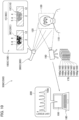
- Noncontact vital sensing is a system that uses a light emitting device to irradiate a subject with visible radiation, near-infrared radiation, or the like, photographs a photographing area of the subject using a camera to obtain image data, and processes this image data using a computer to obtain vital information, for example.
- Vital information includes information on SpO 2 (oxygen saturation measured using a pulse oximeter), blood pressure, pulse waves, and blood vessels deep in a living body, for example.
- the system including a light emitting devices, a camera, and a computer, used for noncontact vital sensing is generally also referred to as a sensing system.
- a conventional light emitting device a device outputting visible radiation, a device outputting visible radiation and near-infrared radiation, and the like are known.
- a camera an RGB camera, a near-infrared camera, or the like is used.
- Vital information obtained using noncontact vital sensing differs depending on the emission spectrum of the output light of the light emitting device. For example, in order to obtain blood pressure information, output light having a high intensity of optical components of a wavelength of 850 nm is preferable. In order to obtain pulse wave information, output light having a high intensity of optical components of a wavelength of 940 nm is preferable. Thus, in noncontact vital sensing, it is preferable to obtain output light having a high intensity of optical components in the near-infrared range.
- Oxygen saturation % C HbO 2 / C HbO 2 + C Hb ⁇ 100 (C (HbO 2 ): concentration of oxyhemoglobin, HbO 2 ; C (Hb): concentration of deoxyhemoglobin Hb)
- Fig. 14 is a diagram illustrating the relationship between wavelengths and extinction coefficients of oxyhemoglobin HbO 2 and deoxyhemoglobin Hb.
- the absorption spectrum of HbO 2 has a small extinction coefficient for red light at a wavelength of around 660 nm, while the absorption spectrum of Hb has a small extinction coefficient in a wavelength range for near-infrared light at a wavelength of around 850 nm.
- the ratio of HbO 2 and Hb can be calculated by measuring the transmitted light in these red light and near-infrared light and calculating the transmission ratio between red light and near-infrared light.
- the red light it is considered also possible to use red light at a wavelength of about 750 nm, for example, instead of red light at a wavelength of about 660 nm.
- the accuracy of vital information obtained using noncontact vital sensing differs depending on the combination of the light emitting device and the camera. Specifically, the accuracy of vital information differs depending on characteristics of the emission spectrum of the output light of the light emitting device and characteristics of the light receiving sensitivity of the camera.
- the combination of a light emitting device that outputs only visible radiation and an RGB camera may not obtain vital information in a dark place, such as at night, and may be susceptible to external disturbances such as body movement and illumination changes.
- a sensing system that combines a light emitting device outputting visible radiation and near-infrared radiation with an RGB camera and a near-infrared camera is known.
- the receiving wavelength range is wider than that of an RGB camera alone, and it is possible to receive light of wavelengths from the visible range to the near-infrared range.
- the reason for combining an RGB camera and a near-infrared camera is that a CMOS image sensor used in an inexpensive RGB camera generally has a low light receiving sensitivity for near-infrared radiation.
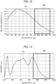
- Fig. 12 is a graph illustrating an example of a light receiving sensitivity curve LR of a CMOS image sensor included in a general RGB camera. As illustrated in Fig. 12 , a general CMOS image sensor has a low light receiving sensitivity in a red to near-infrared range NIR of wavelengths from 750 to 950 nm.
- the sensing system using an RGB camera and a near-infrared camera it becomes possible in a dark place to estimate a heart rate and to obtain vital information such as information on blood vessels deep in a living body.
- vital information such as information on blood vessels deep in a living body.
- this sensing system uses two types of cameras having different configurations, the accuracy of the obtained vital information may easily degrade due to changes in the lighting environment. Specifically, the accuracy of the obtained vital information easily degrades due to a gap in synchronization between the near-infrared radiation output from the near-infrared LED in the light emitting device and the two types of cameras.
- a sensing system combining a light emitting device and one type of CMOS image sensor in demand.
- the sensing system is preferably low-cost. Therefore, the use of a multispectral camera, a hyperspectral camera, and the like that include a general and inexpensive CMOS image sensor and acquire an image including more wavelengths than RGB is being considered.
- a light emitting device having a high emission intensity in the near-infrared range to cover the characteristic of a general CMOS image sensor of the light receiving sensitivity being low in the red to near-infrared range NIR of wavelengths of 750 to 950 nm.
- a light emitting device having the characteristic of an emission spectrum EP 1 illustrated in Fig. 13 is known.
- the emission spectrum EP 1 of this light emitting device the intensity in the red to near-infrared range NIR of wavelengths from 750 to 950 nm is low and decreases at the longer wavelength side.
- the characteristic of the general CMOS image sensor of the light receiving sensitivity being low in the red to near-infrared range NIR as illustrated in Fig. 12 cannot be covered.
- Patent Literature 1 discloses a light emitting device that contains at least Tm or Cr as an active element and has a sharp emission spectrum where the emission peak wavelength is 700 to 1000 nm and the half width of the emission peak waveform is less than 60 nm.
- Patent Literature 1 International Publication No. 2018/143198
- the half width of the emission peak waveform is sharp as less than 60 nm, and thus the overall emission intensity in the near-infrared range cannot be made sufficiently high. Therefore, even when this light emitting device is used, it is not possible to cover the characteristic of the general CMOS image sensor in Fig. 12 of the light receiving sensitivity being low in the near-infrared range. Note that for example, when a phosphor having a fluorescence peak within a wavelength range of 750 nm or more and less than 900 nm is used, it is considered that the intensity of the red to near-infrared range NIR of wavelengths of 750 to 950 nm in the light emitting device can be sufficiently increased.
- An object of the present invention is to provide a phosphor, a light emitting device, a sensing system light source, and a sensing system illumination system, each having a high fluorescence intensity in the red to near-infrared range NIR of wavelengths of 750 to 950 nm.
- a phosphor according to an aspect of the present invention is represented by general formula (1) below.
- Ln is one or more elements selected from La, Pr, Nd, Sm, Eu, Tb, Dy, Ho, Er, Yb, and Lu
- M II is a divalent element
- M III is a trivalent element
- M IV is a tetravalent element
- x, y, and z satisfy 0 ⁇ x ⁇ 0.5, 0 ⁇ y ⁇ 0.5, and 0 ⁇ z ⁇ 0.5.
- a light emitting device includes the phosphor and a solid-state light source having an emission peak on a shorter wavelength side of a fluorescence peak of the phosphor.
- a sensing system light source includes the light emitting device.
- a sensing system illumination system includes the light emitting device.
- a phosphor and a light emitting device will be described below with reference to the drawings.
- a sensing system including a sensing system light source and a sensing system illumination system according to embodiments will also be described with reference to the drawings. Note that dimensional ratios in the drawings are exaggerated for convenience of the description and are sometimes different from actual ratios.
- Fig. 1 is a schematic cross-sectional view illustrating an example of a light emitting device according to a first embodiment.
- Fig. 2 is a schematic cross-sectional view illustrating an example of a light emitting device according to a second embodiment.
- Fig. 3 is a schematic cross-sectional view illustrating an example of a light emitting device according to a third embodiment.
- Fig. 4 is a schematic cross-sectional view illustrating an example of a light emitting device according to a fourth embodiment.
- Fig. 5 is a schematic cross-sectional view illustrating an example of a light emitting device according to a fifth embodiment.
- Fig. 6 is a schematic cross-sectional view illustrating an example of a light emitting device according to a sixth embodiment.
- Fig. 7 is a schematic cross-sectional view illustrating an example of a light emitting device according to a seventh embodiment.
- the light emitting devices 1E to 1G according to the fifth to seventh embodiments further include a light guiding member 15 that guides primary light 6 to a wavelength converter 3, but otherwise respectively have the same configurations as the light emitting devices 1A to 1C according to the first to third embodiments.
- a near-infrared light emitting device 10D of the light emitting device 1D according to the fourth embodiment can further include the light guiding member 15 that guides primary light 6 to the wavelength converter 3.
- the light emitting devices 1A to 1G according to the first to seventh embodiments include: in common a solid-state light source 2 emitting primary light 6; and the wavelength converter 3 including a first phosphor 4 that absorbs the primary light 6 and emits first wavelength-converted light 7 including a near-infrared light component.
- the light emitting devices 1A to 1G according to the first to seventh embodiments can emit output light 90 that includes the first wavelength-converted light 7 including at least the near-infrared light component.
- a phosphor such as the first phosphor 4 included in the wavelength converter 3 emits fluorescence.
- the first phosphor 4 emits the first wavelength-converted light 7 including a near-infrared light component when receiving the primary light 6.
- wavelength converters 3A to 3G of the light emitting devices 1A to 1G can receive primary light 6 and emit output light 90 including at least the primary light 6 and first wavelength-converted light 7 including a near-infrared light component.
- the wavelength converters 3A to 3G included in the light emitting devices 1A to 1G emit near-infrared light-including light 50 or NIR+ ⁇ light 80.
- the near-infrared light-including light 50 is light including the primary light 6 and the first wavelength-converted light 7 including a near-infrared light component.
- the NIR+ ⁇ light 80 is light including the primary light 6, the first wavelength-converted light 7 including a near-infrared light component, and second wavelength-converted light 9.
- the NIR+ ⁇ light 80 is light including the near-infrared light-including light 50 and the second wavelength-converted light 9.
- the light emitting devices 1A to 1G according to the first to seventh embodiments can emit output light 90 including near-infrared light-including light 50 or NIR+ ⁇ light 80, and thus can emit output light 90 including at least the near-infrared light-including light 50.
- the light emitting devices 1C, 1D, and 1G can independently control the light emission of the near-infrared light emitting devices 10C, 10D, or 10G, and the light emission of a white light emitting device 30C, a white light source 35, or a white light emitting device 30G.
- the light emitting devices 1C, 1D, and 1G can emit output light 90 including at least the near-infrared light-including light 50, and can also emit only white light 70 that is derived from the white light emitting device 30C or the like, as output light 90.
- a visible light emitting device 20C, a visible light source 25, and the like are used instead of the white light emitting device 30C, the white light source 35, and the like in the light emitting devices 1C, 1D, and 1G, it becomes possible to emit only visible light 60 that is derived from the visible light emitting device 20C or the like, as output light 90.
- the light emitting device 1D is a light emitting device that combines the near-infrared light emitting device 10D (10) which is a light emitting device emitting near-infrared light, and the white light source 35 which emits white light.
- the light emitting device 1A (1) according to the first embodiment will be described.
- the light emitting device 1A according to the first embodiment includes the solid-state light source 2 and the wavelength converter 3A (3).
- the solid-state light source 2 and the wavelength converter 3A are arranged spaced apart, and this can cause a subject to be irradiated, with a high degree of freedom, with output light 90 including first wavelength-converted light 7 emitted from the wavelength converter 3A.
- Output light 90 includes near-infrared light-including light 50.
- the light emitting device 1A emits near-infrared light-including light 50 that includes primary light 6 and first wavelength-converted light 7 including a near-infrared light component, as output light 90.
- the light emitting device 1A can be said to be a near-infrared light emitting device 10A (10) that emits near-infrared light-including light 50.
- the solid-state light source 2 emits primary light 6.
- Light having a high emission intensity is used as the primary light 6.
- the light having a high emission intensity for example, laser light, light radiated from a high power LED, or the like is used.
- the primary light 6 light including blue light having a spectral distribution maximum intensity within a wavelength range of 400 nm or more and less than 500 nm is used, for example.
- the blue light light having a spectral distribution maximum intensity within a wavelength range of 420 nm or more and less than 480 nm is preferably used.
- the solid-state light source 2 a solid-state light emitting element is used, for example. It is preferable that the solid-state light source 2 be a solid-state light emitting element because of its excellent durability and long life. As the solid-state light source 2, a solid-state light emitting element such as an LED or a laser element is used.
- the solid-state light source 2 emits light in which an emission spectrum E LS has an emission peak EP LS on the shorter wavelength side of a fluorescence peak FP 1 of a fluorescence spectrum F 1 of first wavelength-converted light of the first phosphor 4 included in the wavelength converter 3A (3).
- a having an emission peak EP A on the shorter wavelength side of a fluorescence peak FP B of a fluorescence spectrum F B of B means that the emission peak wavelength of the emission peak EP A of A exists on the shorter wavelength side of the fluorescence peak wavelength of the fluorescence peak FP B of B.
- the fluorescence peak FP 1 means a portion indicating the maximum value when the fluorescence spectrum F 1 of the first phosphor 4 is an aggregate of spectral intensities in increments of 10 nm or less.
- the wavelength converter 3A (3) includes the first phosphor 4 and a sealant 5.
- the first phosphor 4 is included in the sealant 5.
- the first phosphor 4 is represented by general formula (1) below.
- Ln is one or more elements selected from La, Pr, Nd, Sm, Eu, Tb, Dy, Ho, Er, Yb, and Lu
- M II is a divalent element
- M III is a trivalent element
- M IV is a tetravalent element
- x, y, and z satisfy 0 ⁇ x ⁇ 0.5, 0 ⁇ y ⁇ 0.5, and 0 ⁇ z ⁇ 0.5.
- A', B', and C' are atoms constituting the host crystal of the garnet crystal structure.
- A' is an "A-site”
- the structure including the "A-site” is an A-site structure in which oxygen atoms O are dodecahedrally coordinated around an atom A'.
- B' is a "B-site”
- the structure including the "B-site” is a B-site structure in which oxygen atoms O are octahedrally coordinated around an atom B'.
- C' is a "C-site”
- the structure including the "C-site” is a C-site structure in which oxygen atoms O are tetrahedrally coordinated around an atom C'.
- General formula (1) corresponds to general formula (2) in which Gd is included in the "A site”, M III is included in the “B site”, and Ga is included in the "C site” as essential components.
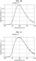
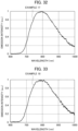
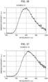
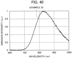
- the first wavelength-converted light 7 has a fluorescence peak within a wavelength range of 750 nm or more and less than 900 nm.
- Ln, M II, M III , and M IV be the above elements in general formula (1) because highly accurate sensing can be achieved by compensating for the low sensitivity in the near-infrared range of an image sensor with a CMOS using Si, or the like.
- M II is preferably a divalent element, and more preferably contains at least one of Ca or Sr. It is preferable that M II be one of these elements because the internal quantum efficiency IQE of the first wavelength-converted light 7 tends to be high.
- M III is preferably a trivalent element other than Gd and Ln, and more preferably contains at least one of Ga or Sc. It is preferable that M III be one of these elements because the internal quantum efficiency IQE of the first wavelength-converted light 7 tends to be high.
- M IV is preferably a tetravalent element, and more preferably contains at least one of Si or Ge. It is preferable that M IV be one of these elements because the internal quantum efficiency IQE of the first wavelength-converted light 7 tends to be high.
- M II be a divalent element
- M III be a trivalent element other than Gd and Ln
- M IV be a tetravalent element. It is preferable that general formula (1) have a combination of these elements, the internal quantum efficiency IQE of the first wavelength-converted light 7 tends to be high.
- M II contain at least one of Ca or Sr
- M III contain at least one of Ga or Sc
- M IV contain at least one of Si or Ge. It is preferable that general formula (1) have a combination of these elements because the internal quantum efficiency IQE of the first wavelength-converted light 7 tends to be higher.
- M II contain at least one of Ca or Sr
- M IV contain Ge. It is preferable that general formula (1) have a combination of these elements because the internal quantum efficiency IQE of the first wavelength-converted light 7 tends to be even higher.
- M II contain Sr and M IV contain at least one of Si or Ge. It is preferable that general formula (1) have a combination of these elements because the internal quantum efficiency IQE of the first wavelength-converted light 7 tends to be even higher.
- M II contain Sr and M IV contain Ge. It is preferable that general formula (1) have a combination of these elements because the internal quantum efficiency IQE of the first wavelength-converted light 7 tends to be particularly high.
- x and z satisfy x - 0.1 ⁇ z ⁇ x + 0.1 in general formula (1) because the charge balance of the first phosphor 4 represented by general formula (1) is maintained and the structure of the first phosphor 4 is stable.
- Ln is one or more elements selected from La, Pr, Nd, Sm, Eu, Tb, Dy, Ho, Er, Yb, and Lu
- M II is a divalent element
- M III is a trivalent element
- M IV is a tetravalent element
- x, y, and z satisfy 0 ⁇ x ⁇ 0.5, 0 ⁇ y ⁇ 0.5, and 0 ⁇ z ⁇ 0.5, and 0.001 ⁇ p ⁇ 0.1.
- p preferably satisfies 0.005 ⁇ p ⁇ 0.08, and more preferably satisfies 0.01 ⁇ p ⁇ 0.05. It is preferable that p be within the above ranges because the external quantum efficiency EQE tends to be high.
- the first wavelength-converted light 7 has the fluorescence peak FP 1 within a wavelength range of 750 nm or more and less than 900 nm.
- the first wavelength-converted light 7 has the fluorescence peak FP 1 preferably within a wavelength range of 770 nm or more and less than 900 nm, and more preferably within a wavelength range of 780 nm or more and less than 900 nm.
- the fluorescence spectrum F 1 of the first wavelength-converted light 7 have the fluorescence peak FP 1 within the above wavelength ranges because only light in the red to near-infrared range is emitted which is suitable for acquiring vital information, such as information about blood pressure, pulse waves, and blood vessels deep in a living body.
- the fluorescence spectrum F 1 of the first wavelength-converted light 7 have the fluorescence peak FP 1 within a wavelength range of 900 nm or more because light energy is easily wasted by emitting light in a wavelength range where the light receiving sensitivity of a general CMOS image sensor is very low.
- the full width at half maximum of the fluorescence peak FP 1 within a wavelength range of 750 nm or more and less than 900 nm is usually 110 nm or more and less than 250 nm.
- the full width at half maximum of the fluorescence peak FP 1 is preferably 120 nm or more and less than 220 nm.
- the full width at half maximum of the fluorescence peak FP 1 be within the above ranges because the fluorescence peak FP 1 is broad and thus highly accurate sensing can be achieved by widely compensating for the low sensitivity in the near-infrared range of an image sensor with a CMOS using Si, or the like.
- the full width at half maximum of the fluorescence peak FP 1 exceeds 250 nm, the efficiency of light use may be reduced.
- the 1/e afterglow value is generally 1 ⁇ s or more and less than 100 ⁇ s. In the first wavelength-converted light 7, the 1/e afterglow value is preferably 1 ⁇ s or more and less than 80 ⁇ s.
- the 1/e afterglow value means a time until the emission intensity becomes 1/e. It is preferable that the 1/e afterglow value of the first wavelength-converted light 7 be within the above ranges because the output and stop of the near-infrared light can be controlled with good responsiveness to the output and stop operation of the primary light 6 emitted from the solid-state light source 2.
- the first phosphor 4 is included in the sealant 5.
- the first phosphor 4 is dispersed in the sealant 5.
- the first phosphor 4 it becomes possible to efficiently absorb the primary light 6 emitted by the solid-state light source 2 and efficiently convert the wavelength thereof to that of near-infrared light.
- the first phosphor 4 it becomes easier to form the wavelength converter 3 into a sheet or film shape.
- the sealant 5 is made from at least one of an organic material or an inorganic material.
- the sealant 5 is preferably made from at least one of a transparent (translucent) organic material or a transparent (translucent) inorganic material.
- An example of the organic material sealant is a transparent organic material, such as silicone resin.
- An example of the inorganic material sealant is a transparent inorganic material, such as low melting point glass.
- the wavelength converter 3 is preferably made from an inorganic material.
- An inorganic material here means a material other than an organic material, and includes ceramics and metals as a concept.
- the thermal conductivity thereof is higher than that of the wavelength converter including an organic material such as a sealing resin, and this facilitates the heat dissipation design.
- the temperature rise of the wavelength converter 3 can be effectively suppressed. Consequently, the temperature quenching of the first phosphor 4 in the wavelength converter 3 is suppressed, and it becomes possible to achieve high output of emitted light.
- the sealant 5 is preferably made from an inorganic material.
- the inorganic material for the sealant 5 is preferably zinc oxide (ZnO).
- ZnO zinc oxide
- a wavelength converter without the sealant 5 can be used instead of the wavelength converter 3.
- particles of the first phosphor 4 be fixed to each other using an organic or inorganic binder.
- Particles of the first phosphor 4 can also be fixed to each other through a heating reaction of the first phosphor 4.
- a generally used resin-based adhesive, ceramic fine particles, low-melting-point glass, or the like can be used as the binder.
- the primary light 6 emitted from the solid-state light source 2 is emitted on a front surface 3a of the wavelength converter 3A.
- the emitted primary light 6 penetrates the wavelength converter 3A.
- the first phosphor 4 included in the wavelength converter 3A absorbs part of the primary light 6 and emits the first wavelength-converted light 7.
- the output light 90 including the primary light 6 and the first wavelength-converted light 7 is emitted from a back surface 3b of the wavelength converter 3A.
- the first wavelength-converted light 7 includes a near-infrared light component having a fluorescence peak within a wavelength range of 750 nm or more and less than 900 nm.
- the output light 90 output from the light emitting device 1A is near-infrared light-including light 50 which is light including primary light 6 and first wavelength-converted light 7 including a near-infrared light component.
- the first phosphor 4 included in the wavelength converter 3A of the light emitting device 1A emits first wavelength-converted light 7 including a large amount of a near-infrared light component.
- the wavelength converter 3A of the light emitting device 1A emits near-infrared light-including light 50 including a near-infrared light component, as output light 90.
- the light emitting device 1A can provide a phosphor and a light emitting device that have a high fluorescence intensity in the red to near-infrared range NIR of wavelengths of 750 to 950 nm.
- the light emitting device 1A can be used for a sensing system light source 100A and a sensing system illumination system 300A described below.
- the light emitting device 1A can provide a sensing system light source and a sensing system illumination system that have a high fluorescence intensity in the red to near-infrared range NIR of wavelengths of 750 to 950 nm.
- the light emitting device 1B (1) according to a second embodiment will be described.
- the light emitting device 1B according to the second embodiment includes the solid-state light source 2 and the wavelength converter 3B (3).
- the light emitting device 1B according to the second embodiment uses the wavelength converter 3B instead of the wavelength converter 3A of the light emitting device 1A according to the first embodiment.
- the wavelength converter 3B further includes a second phosphor 8.
- the light emitting device 1B emits NIR+ ⁇ light 80 that includes near-infrared light-including light 50 including primary light 6 and first wavelength-converted light 7, and second wavelength-converted light 9 which is a light component other than the near-infrared light-including light 50.
- the light emitting device 1B can be said to be an NIR+ ⁇ light emitting device 40B (40) that emits NIR+ ⁇ light 80.
- the wavelength converter 3B includes the first phosphor 4, the second phosphor 8, and the sealant 5.
- the first phosphor 4 and the second phosphor 8 are included in the sealant 5. That is, the wavelength converter 3B of the light emitting device 1B further includes the second phosphor 8 that absorbs primary light 6 and converts it into second wavelength-converted light 9 different from the first wavelength-converted light 7.
- the wavelength converter 3B includes the first phosphor 4 and the second phosphor 8 having an emission peak wavelength different from the emission peak wavelength of the first phosphor 4.
- the wavelength converter 3B is the same as the wavelength converter 3A of the light emitting device 1 according to the first embodiment except that it further includes the second phosphor 8.
- the second phosphor 8 is mainly described below, and the description of other configurations and actions will be omitted or simplified.
- the light emitting device 1B including the wavelength converter 3B includes the wavelength converter 3B and the solid-state light source 2 having an emission peak on the shorter wavelength side of the emission peak of the first phosphor 4 and the emission peak of the second phosphor 8.
- the light emitting device 1B includes the first phosphor 4, the second phosphor 8, and the solid-state light source 2.
- the second phosphor 8 is a phosphor having a fluorescence peak wavelength different from the fluorescence peak wavelength of the first phosphor 4.
- the fluorescence peak wavelength of the first phosphor 4 is the wavelength of the fluorescence peak FP 1 in the fluorescence spectrum F 1 of the first wavelength-converted light 7.
- the fluorescence peak wavelength of the second phosphor 8 is the wavelength of the fluorescence peak FP 2 in the fluorescence spectrum E 2 of the second wavelength-converted light 9.
- the second phosphor 8 is a phosphor having the peak wavelength of the fluorescence peak FP 2 of the second wavelength-converted light 9, which is different from the peak wavelength of the fluorescence peak FP 1 of the first wavelength-converted light 7 of the first phosphor 4.
- the second phosphor 8 for example, a phosphor is used in which the peak wavelength of the fluorescence peak FP 2 of the second wavelength-converted light 9 is on the shorter wavelength side of the peak wavelength of the fluorescence peak FP 1 of the first wavelength-converted light 7 of the first phosphor 4.
- the second wavelength-converted light 9 emitted from such a second phosphor 8 for example, visible light, white light, or the like is used.
- NIR+ ⁇ light 80 that includes near-infrared light-including light 50 including the primary light 6 and the first wavelength-converted light 7, and second wavelength-converted light 9 which is a light component other than the near-infrared light-including light 50.
- NIR+ ⁇ light 80 means light including near-infrared light-including light 50 and a light component other than the near-infrared light-including light 50.
- the second wavelength-converted light 9 is visible light 60 such as white light 70
- NIR+ ⁇ light 80 is light including the near-infrared light-including light 50 and the visible light 60 such as the white light 70.
- the light emitting device 1B can emit, as output light 90, NIR+ ⁇ light 80 including near-infrared light-including light 50 and a light component other than the near-infrared light-including light 50.
- the wavelength converter 3B further includes the second phosphor 8 in addition to the first phosphor 4, the shape and excitation characteristics of the fluorescence spectrum emitted from the wavelength converter 3B can be controlled.
- the obtained light emitting device 1B it becomes possible for the obtained light emitting device 1B to easily adjust the spectral distribution of the output light according to the application.
- the second phosphor 8 is not particularly limited as long as the fluorescence peak wavelength of the fluorescence peak FP 2 in the fluorescence spectrum F 2 of the second wavelength-converted light 9 is different from the fluorescence peak wavelength of the fluorescence peak FP 1 in the fluorescence spectrum F 1 of the first wavelength-converted light 7 of the first phosphor 4.
- the second phosphor 8 preferably includes a phosphor of a garnet crystal structure containing Ce 3+ . It is preferable that the second phosphor 8 include a phosphor of a garnet crystal structure containing Ce 3+ because it has a fluorescence peak wavelength from 500 to 600 nm, resulting in broad emission in a wide band.
- the phosphor of a garnet crystal structure containing Ce 3+ for example, Y 3 Al 5 O 12 :Ce 3+ , Y 3 (Al, Ga) 5 O 12 :Ce 3+ , Lu 3 Al 5 O 12 :Ce 3+ , Lu 2 CaMg 2 Si 3 O 12 :Ce 3+ , or the like is used.
- a second phosphor 8 including such a phosphor of a garnet crystal structure containing Ce 3+ is used, it becomes possible to obtain output light having a large amount of light components from green-based to yellow-based light components.
- Such a second phosphor 8 absorbs light well within a wavelength range of 430 or more and 480 nm or less to convert it with high efficiency to green-based to yellow-based light having the maximum intensity value within a wavelength range of 500 or more and less than 600 nm.
- a solid-state light source 2 that emits blue light as the primary light 6 and then using the second phosphor 8.
- the first phosphor 4 emit the first wavelength-converted light 7 by absorbing at least one of the primary light 6 emitted by the solid-state light source 2 or the second wavelength-converted light 9 emitted by the second phosphor 8.
- the first phosphor 4 be a phosphor that absorbs the primary light 6 emitted by the solid-state light source 2 and emits the first wavelength-converted light 7, which is near-infrared light.
- the first phosphor 4 may be a phosphor that absorbs the second wavelength-converted light 9 emitted by the second phosphor 8 and emits the first wavelength-converted light 7, which is near-infrared light. That is, the second phosphor 8 may be excited by the primary light 6 to emit the second wavelength-converted light 9, and the first phosphor 4 may be excited by the second wavelength-converted light 9 to emit the first wavelength-converted light 7. In this case, even when the first phosphor 4 is a phosphor that is hardly excited by the primary light 6, by means of the second phosphor 8, it becomes possible for the first phosphor 4 to be excited by the fluorescence emitted by the second phosphor 8.
- the first phosphor 4 absorbs the second wavelength-converted light 9 and emits the first wavelength-converted light 7, it becomes possible to select as the first phosphor 4 a phosphor that absorbs the visible light, and this broadens the choice of the first phosphor 4 and facilitates the industrial production of the light emitting device 1B.
- the first phosphor 4 absorbs the second wavelength-converted light 9 and emits the first wavelength-converted light 7, it becomes possible for the light emitting device 1B to emit first wavelength-converted light 7 having a large near-infrared light component intensity.
- the second phosphor 8 may include two or more types of phosphor of a garnet crystal structure containing Ce 3+ . It is preferable that the second phosphor 8 contain two or more types of Ce 3+ -activated phosphor because a more broadband light emission is achieved.
- the primary light 6 emitted from the solid-state light source 2 is emitted on the front surface 3a of the wavelength converter 3B.
- the emitted primary light 6 penetrates the wavelength converter 3B.
- the second phosphor 8 included in the wavelength converter 3B absorbs part of the primary light 6 and emits the second wavelength-converted light 9.
- the first phosphor 4 included in the wavelength converter 3B absorbs part of the primary light 6 and/or part of the second wavelength-converted light 9 and emits the first wavelength-converted light 7.
- the output light 90 including the primary light 6, the first wavelength-converted light 7, and the second wavelength-converted light 9 is emitted from the back surface 3b of the wavelength converter 3B.
- the first wavelength-converted light 7 includes a near-infrared light component having a fluorescence peak within a wavelength range of 750 nm or more and less than 900 nm.
- the output light 90 output from the light emitting device 1B is NIR+ ⁇ light 80 that is light including primary light 6, first wavelength-converted light 7 including the near-infrared light component, and second wavelength-converted light 9.
- the first phosphor 4 included in the wavelength converter 3B of the light emitting device 1B emits first wavelength-converted light 7 including a large amount of the near-infrared light component.
- the wavelength converter 3B of the light emitting device 1B emits NIR+ ⁇ light 80 including the near-infrared light component, as output light 90.
- the light emitting device 1B achieves the same effect as that of the light emitting device 1A according to the first embodiment.
- the wavelength converter 3B of the light emitting device 1B further includes the second phosphor 8
- the light emitting device 1B emits, as output light 90, NIR+ ⁇ light 80 including near-infrared light-including light 50 and visible light 60 such as white light 70.
- the light emitting device 1B can be used as an illumination device.
- the light emitting device 1B can output near-infrared light-including light 50 having a wider band by combining visible light 60 such as white light 70 and the near-infrared light-including light 50.
- the light emitting device 1C (1) according to the third embodiment will be described.
- the light emitting device 1C according to the third embodiment includes the near-infrared light emitting device 10C (10) that is a device emitting near-infrared light-including light 50, and the white light emitting device 30C (30) that is a device emitting white light 70.
- the light emitting device 1C is a light emitting device including the near-infrared light emitting device 10C (10) that is a light emitting device emitting near-infrared light, and the white light emitting device 30C (30) that is a light emitting device emitting white light.
- the light emitting device 1C emits, as output light 90, NIR+ ⁇ light 80 that includes: near-infrared light-including light 50 including primary light 6 and first wavelength-converted light 7; and second wavelength-converted light 9 that is a light component other than the near-infrared light-including light 50.
- the light emitting device 1C can be said to be an NIR+ ⁇ light emitting device 40C (40) that emits NIR+ ⁇ light 80.
- the near-infrared light emitting device 10C is a device that emits near-infrared light-including light 50.
- the near-infrared light emitting device 10C includes the solid-state light source 2 and the wavelength converter 3C (3). Note that the solid-state light source 2 and the wavelength converter 3C of the near-infrared light emitting device 10C have the same structures as those of the solid-state light source 2 and the wavelength converter 3A of the light emitting device 1A according to the first embodiment, respectively. That is, the near-infrared light emitting device 10C has the same structure as that of the light emitting device 1A according to the first embodiment.
- the output light 90 output from the near-infrared light emitting device 10C is near-infrared light-including light 50 that is light including primary light 6 and first wavelength-converted light 7 including a near-infrared light component.
- the white light emitting device 30C is a device that emits white light 70.
- the white light emitting device 30C includes the solid-state light source 2 and a white light wavelength converter 33C (33).
- the solid-state light source 2 of the white light emitting device 30C has the same configuration as that of the solid-state light source 2 of the light emitting device 1A according to the first embodiment.
- the solid-state light source 2 included in the near-infrared light emitting device 10C and the solid-state light source 2 included in the white light emitting device 30C may have the same characteristic or different characteristics.
- the white light emitting device 30C is a device that emits white light 70
- the visible light emitting device 20C (20) emitting visible light 60 may be used, as necessary, instead of the white light emitting device 30C, as a modified example.
- the visible light emitting device 20C includes the solid-state light source 2 and a visible light wavelength converter 23C (23).
- the visible light emitting device 20C can be manufactured by changing, for example, the solid-state light source 2, the second phosphor 8 in the white light wavelength converter 33C, and the like, making up the white light emitting device 30C.
- the white light wavelength converter 33C (33) includes the second phosphor 8 and the sealant 5.
- the white light wavelength converter 33C corresponds to one obtained by replacing all of the first phosphor 4 with the second phosphor 8 in the wavelength converter 3B included in the light emitting device 1B according to the second embodiment.
- the white light wavelength converter 33C is the same as the wavelength converter 3B included in the light emitting device 1B according to the second embodiment except that all of the first phosphor 4 is replace with the second phosphor 8. Thus, the description of the structure and action will be omitted or simplified hereinafter.
- the visible light wavelength converter 23C (23) may be used instead of the white light wavelength converter 33C.
- the visible light wavelength converter 23C like the white light wavelength converter 33C, includes the second phosphor 8 and the sealant 5.
- the visible light wavelength converter 23C can be manufactured by changing the second phosphor 8 and the like in the white light wavelength converter 33C.
- the action of the light emitting device 1C will be described. As illustrated in Fig. 3 , the action of the light emitting device 1C is a combination of the action of the near-infrared light emitting device 10C and the action of the white light emitting device 30C.
- the action of the near-infrared light emitting device 10C is the same as that of the light emitting device 1A according to the first embodiment except that output light 90 is not emitted. That is, first, the primary light 6 emitted from the solid-state light source 2 is emitted on a front surface 3a of the wavelength converter 3C. The emitted primary light 6 penetrates the wavelength converter 3C. When the primary light 6 penetrates the wavelength converter 3C, the first phosphor 4 included in the wavelength converter 3C absorbs part of the primary light 6 and emits the first wavelength-converted light 7. In this way, near-infrared light-including light 50 including the primary light 6 and the first wavelength-converted light 7 is emitted from a back surface 3b of the wavelength converter 3C.
- the action of the white light wavelength converter 33C is the same as that of the light emitting device 1B according to the second embodiment except that there is no action by the first phosphor 4 and output light 90 is not emitted. That is, first, primary light 6 emitted from the solid-state light source 2 is emitted on a front face 3a of the white light wavelength converter 33C. The emitted primary light 6 penetrates the white light wavelength converter 33C. When the primary light 6 penetrates the white light wavelength converter 33C, the second phosphor 8 included in the white light wavelength converter 33C absorbs part of the primary light 6 and emits the second wavelength-converted light 9. In this way, white light 70 that is light including the primary light 6 and the second wavelength-converted light 9 is emitted from a back surface 3b of the white light wavelength converter 33C.
- the action of the light emitting device 1C is a combination of the action of the near-infrared light emitting device 10C and the action of the white light emitting device 30C.
- the action of the light emitting device 1C is the sum of the action of the near-infrared light emitting device 10C and the action of the white light emitting device 30C.
- the action of the light emitting device 1C is the action of the near-infrared light emitting device 10C or the action of the white light emitting device 30C.
- the light emitting device 1C emits NIR+ ⁇ light 80 that includes: near-infrared light-including light 50 which includes primary light 6 and first wavelength-converted light 7; and white light 70 which is light including primary light 6 and second wavelength-converted light 9.
- the action of the visible light wavelength converter 23C is as follows. That is, first, primary light 6 emitted from the solid-state light source 2 is emitted on a front face 3a of the visible light wavelength converter 23C. The emitted primary light 6 penetrates the visible light wavelength converter 23C. When the primary light 6 penetrates the visible light wavelength converter 23C, the second phosphor 8 included in the visible light wavelength converter 23C absorbs part of the primary light 6 and emits second wavelength-converted light 9. Thus, visible light 60 that is light including the primary light 6 and the second wavelength-converted light 9 is emitted from a back surface 3b of the visible light wavelength converter 23C.
- the light emitting device 1C emits NIR+ ⁇ light 80 that includes: near-infrared light-including light 50 which includes primary light 6 and first wavelength-converted light 7; and visible light 60 which is light including primary light 6 and second wavelength-converted light 9.
- the first wavelength-converted light 7 includes a near-infrared light component having a fluorescence peak within a wavelength range of 750 nm or more and less than 900 nm.
- output light 90 output from the light emitting device 1C is NIR+ ⁇ light 80 that is light including primary light 6, first wavelength-converted light 7 including the near-infrared light component, and second wavelength-converted light 9.
- the first phosphor 4 contained in the wavelength converter 3C included in the near-infrared light emitting device 10C of the light emitting device 1C emits first wavelength-converted light 7 including a large amount of a near-infrared light component.
- the white light wavelength converter 33C included in the white light emitting device 30C of the light emitting device 1C emits white light 70.
- the light emitting device 1C emits NIR+ ⁇ light 80 including the near-infrared light component, as output light 90.
- the visible light wavelength converter 23C included in the visible light emitting device 20C of the light emitting device 1C emits visible light 60.
- the light emitting device 1C emits NIR+ ⁇ light 80 including the near-infrared light component, as output light 90.
- the light emitting device 1C achieves the same effect as that of the light emitting device 1A according to the first embodiment.
- the light emitting device 1C can be used as an illumination device as the light emitting device 1B according to the second embodiment, and can output near-infrared light-including light 50 having a wider band.
- the light emitting device 1C at least one of the near-infrared light emitting device 10C or the white light emitting device 30C can be operated.
- the light emitting device 1C can change the intensity ratio between near-infrared light-including light 50 and white light 70.
- the visible light emitting device 20C when used instead of the white light emitting device 30C, at least one of the near-infrared light emitting device 10C or the visible light emitting device 20C can be operated in the light emitting device 1C.
- the light emitting device 1C using the visible light emitting device 20C instead of the white light emitting device 30C can change the intensity ratio between near-infrared light-including light 50 and visible light 60.
- the light emitting device 1D (1) according to the fourth embodiment will be described.
- the light emitting device 1D according to the fourth embodiment includes the near-infrared light emitting device 10D (10) that is a device emitting near-infrared light-including light 50, and the white light source 35 that is a light source emitting white light 70.
- the light emitting device 1D is a light emitting device including: the near-infrared light emitting device 10D (10) that is a light emitting device emitting near-infrared light; and the white light source 35 that is a light source emitting white light 70.
- the light emitting device 1D differs from the light emitting device 1C according to the third embodiment in that the white light source 35 is used instead of the white light emitting device 30C, and the other points are the same.
- the white light source 35 will be mainly described below, and the description of other configurations and actions will be omitted or simplified.
- the light emitting device 1D emits, as output light 90, NIR+ ⁇ light 80 that includes: near-infrared light-including light 50 which includes primary light 6 and first wavelength-converted light 7; and second wavelength-converted light 9 which is a light component other than the near-infrared light-including light 50.
- the light emitting device 1D can be said to be an NIR+ ⁇ light emitting device 40D (40) that emits the NIR+ ⁇ light 80.
- the near-infrared light emitting device 10D includes the solid-state light source 2 and the wavelength converter 3D (3).
- the solid-state light source 2 and the wavelength converter 3D of the near-infrared light emitting device 10D have the same structures as those of the solid-state light source 2 and the wavelength converter 3C of the near-infrared light emitting device 10C included in the light emitting device 1C according to the third embodiment, respectively.
- the solid-state light source 2 and the wavelength converter 3D of the near-infrared light emitting device 10D have the same structures as those of the solid-state light source 2 and the wavelength converter 3A of the light emitting device 1A according to the first embodiment.
- Output light 90 output from the near-infrared light emitting device 10D is near-infrared light-including light 50 that is light including primary light 6 and first wavelength-converted light 7 including a near-infrared light component.
- the white light source 35 is a light source that emits white light 70.
- a known light source can be used.
- the white light source 35 is a light source that emits white light 70, as necessary, the visible light source 25 that emits visible light 60 may be used instead of the white light source 35, as a modified example.
- the visible light source 25 a known light source can be used.
- the action of the light emitting device 1D will be described. As illustrated in Fig. 4 , the action of the light emitting device 1D is a combination of the action of the light emitting device 1C according to the third embodiment and the action of the white light source 35.
- the action of the near-infrared light emitting device 10D is the same as that of the near-infrared light emitting device 10C included in the light emitting device 1C according to the third embodiment. That is, first, primary light 6 emitted from the solid-state light source 2 is emitted on a front face 3a of the wavelength converter 3D. The emitted primary light 6 penetrates the wavelength converter 3D. When the primary light 6 penetrates the wavelength converter 3D, the first phosphor 4 included in the wavelength converter 3D absorbs part of the primary light 6 and emits first wavelength-converted light 7. Thus, the near-infrared light-including light 50 including the primary light 6 and the first wavelength-converted light 7 is emitted from a back surface 3b of the wavelength converter 3D.
- the action of the white light source 35 is an action of emitting white light 70.
- the action of the light emitting device 1D is a combination of the action of the near-infrared light emitting device 10D and the action of the white light source 35.
- the action of the light emitting device 1D is the sum of the action of the near-infrared light emitting device 10D and the action of the white light source 35.
- the action of the light emitting device 1D is the action of the near-infrared light emitting device 10D or the action of the white light source 35.
- the light emitting device 1D When the near-infrared light emitting device 10D and the white light source 35 are operated together, the light emitting device 1D emits NIR+ ⁇ light 80 that includes: near-infrared light-including light 50 including the primary light 6 and the first wavelength-converted light 7; and the white light 70.
- the action of the visible light source 25 is the action of emitting visible light 60.
- the light emitting device 1D emits the NIR+ ⁇ light 80 that includes: near-infrared light-including light 50 including primary light 6 and first wavelength-converted light 7; and visible light 60.
- the first wavelength-converted light 7 includes a near-infrared light component having a fluorescence peak within a wavelength range of 750 nm or more and less than 900 nm.
- output light 90 output from the light emitting device 1D is NIR+ ⁇ light 80 that includes primary light 6, first wavelength-converted light 7 including the near-infrared light component, and white light 70.
- output light 90 output from the light emitting device 1D is NIR+ ⁇ light 80 that includes primary light 6, first wavelength-converted light 7 including the near-infrared light component, and visible light 60.
- the first phosphor 4 contained in the wavelength converter 3D included in the near-infrared light emitting device 10D of the light emitting device 1D emits first wavelength-converted light 7 including a large amount of the near-infrared light component.
- the white light source 35 of the light emitting device 1D emits white light 70.
- the light emitting device 1D emits NIR+ ⁇ light 80 including the near-infrared light component, as output light 90.
- the visible light source 25 When the visible light source 25 is used instead of the white light source 35 in the light emitting device 1D, the visible light source 25 of the light emitting device 1D emits visible light 60.
- the light emitting device 1D when the near-infrared light emitting device 10D and the visible light source 25 are operated together, the light emitting device 1D emits NIR+ ⁇ light 80 including the near-infrared light component, as output light 90.
- the light emitting device 1D achieves the same effect as that of the light emitting device 1A according to the first embodiment.
- the light emitting device 1D can be used as an illumination device as the light emitting device 1B according to the second embodiment, and can output near-infrared light-including light 50 having a wider band.
- the light emitting device 1D at least one of the near-infrared light emitting device 10D or the white light source 35 can be operated.
- the light emitting device 1D can change the intensity ratio between the near-infrared light-including light 50 and the white light 70.
- the visible light source 25 is used instead of the white light source 35
- at least one of the near-infrared light emitting device 10D or the visible light source 25 can be operated in the light emitting device 1D.
- the light emitting device 1D using the visible light source 25 instead of the white light source 35 can change the intensity ratio between near-infrared light-including light 50 and visible light 60.
- the light emitting device 1E (1) according to the fifth embodiment will be described.
- the light emitting device 1E according to the fifth embodiment includes the solid-state light source 2, the wavelength converter 3E (3), and a light guiding member 15.
- the light emitting device 1E according to the fifth embodiment is obtained by adding the light guiding member 15 to the light emitting device 1A according to the first embodiment.
- the light emitting device 1E according to the fifth embodiment differs from the light emitting device 1A according to the first embodiment only in the light guiding member 15.
- the light guiding member 15 will be mainly described below, and the description of configurations and actions of other members will be omitted or simplified.
- the solid-state light source 2 and the wavelength converter 3E are arranged spaced apart in such a manner that the primary light 6 emitted from the solid-state light source 2 passes through the inside of the light guiding member 15 to be emitted to the wavelength converter 3E.
- the light guiding member 15 is a member arranged between the solid-state light source 2 and the wavelength converter 3E to guide primary light 6 to the wavelength converter 3E.
- the primary light 6 is to pass through the inside of the light guiding member 15.
- the solid-state light source 2 and the wavelength converter 3E are arranged spaced apart.
- the light guiding member 15 allows the primary light 6 emitted by the solid-state light source 2 to pass through the inside of the light guiding member 15 to be emitted on the wavelength converter 3E.
- the primary light 6 can be efficiently guided to the wavelength converter 3E even when the solid-state light source 2 and the wavelength converter 3E are arranged spaced apart.
- an optical fiber or the like is used as the light guiding member 15.
- the light emitting device 1E will be described. As illustrated in Fig. 5 , first, primary light 6 emitted from the solid-state light source 2 passes through the inside of the light guiding member 15 to be emitted on a front face 3a of the wavelength converter 3E. The emitted primary light 6 penetrates the wavelength converter 3E. When the primary light 6 penetrates the wavelength converter 3E, the first phosphor 4 included in the wavelength converter 3E absorbs part of the primary light 6 and emits the first wavelength-converted light 7. In this way, the output light 90 including the primary light 6 and the first wavelength-converted light 7 is emitted from the back surface 3b of the wavelength converter 3E.
- the first wavelength-converted light 7 includes a near-infrared light component having a fluorescence peak within a wavelength range of 750 nm or more and less than 900 nm.
- output light 90 output from the light emitting device 1E is near-infrared light-including light 50 that includes primary light 6 and first wavelength-converted light 7 including the near-infrared light component.
- the wavelength converter 3E of the light emitting device 1E Since the first phosphor 4 included in the wavelength converter 3E of the light emitting device 1E emits the first wavelength-converted light 7 including a large amount of a near-infrared light component, the wavelength converter 3E of the light emitting device 1E emits output light 90 including the near-infrared light component.
- the light emitting device 1E achieves the same effect as that of the light emitting device 1A according to the first embodiment.
- the light emitting device 1E includes the light guiding member 15, it is possible to have a configuration in which the solid-state light source 2 and the wavelength converter 3 are separated in distance. Thus, with the light emitting device 1E, the degree of freedom in designing the arrangement of the solid-state light source 2 and the wavelength converter 3 in the light emitting device 1 becomes relatively large.
- the light emitting device 1F (1) according to the sixth embodiment will be described.
- the light emitting device 1F according to the sixth embodiment includes the solid-state light source 2, the wavelength converter 3F (3), and the light guiding member 15.
- the light emitting device 1F according to the sixth embodiment is obtained by adding the light guiding member 15 to the light emitting device 1B according to the second embodiment.
- the light emitting device 1F according to the sixth embodiment differs from the light emitting device 1B according to the second embodiment only in the light guiding member 15.
- the light guiding member 15 is the same as that used in the light emitting device 1E according to the fifth embodiment. Thus, only the action of the light emitting device 1F will be described below, and the description of constituent members will be omitted or simplified.
- the solid-state light source 2 and the wavelength converter 3F are arranged spaced apart in such a manner that the primary light 6 emitted from the solid-state light source 2 passes through the inside of the light guiding member 15 to be emitted to the wavelength converter 3F.
- the light emitting device 1F emits, as output light 90, NIR+ ⁇ light 80 that includes: near-infrared light-including light 50 which includes primary light 6 and first wavelength-converted light 7; and second wavelength-converted light 9 which is a light component other than the near-infrared light-including light 50.
- the light emitting device 1F can be said to be an NIR+ ⁇ light emitting device 40F (40) that emits the NIR+ ⁇ light 80.
- the primary light 6 emitted from the solid-state light source 2 passes through the inside of the light guiding member 15 to be emitted on a front face 3a of the wavelength converter 3F.
- the emitted primary light 6 penetrates the wavelength converter 3F.
- the second phosphor 8 included in the wavelength converter 3F absorbs part of the primary light 6 and emits the second wavelength-converted light 9.
- the first phosphor 4 included in the wavelength converter 3F absorbs part of the primary light 6 and/or part of the second wavelength-converted light 9 to emit the first wavelength-converted light 7.
- the output light 90 including the primary light 6, the first wavelength-converted light 7, and the second wavelength-converted light 9 is emitted from a back surface 3b of the wavelength converter 3F.
- the first wavelength-converted light 7 includes a near-infrared light component having a fluorescence peak within a wavelength range of 750 nm or more and less than 900 nm.
- output light 90 output from the light emitting device 1F is NIR+ ⁇ light 80 that includes the primary light 6, the first wavelength-converted light 7 including the near-infrared light component, and the second wavelength-converted light 9.
- the first phosphor 4 included in the wavelength converter 3F of the light emitting device 1F emits the first wavelength-converted light 7 including a large amount of the near-infrared light component, and thus the wavelength converter 3F of the light emitting device 1F emits the NIR+ ⁇ light 80 including the near-infrared light component, as output light 90.
- the light emitting device 1F achieves the same effect as that of the light emitting device 1A according to the first embodiment.
- the wavelength converter 3F of the light emitting device 1F further includes the second phosphor 8, it becomes possible for the light emitting device 1F to easily adjust the spectral distribution of the output light according to the application.
- the light emitting device 1F includes the light guiding member 15, it is possible to have a configuration in which the solid-state light source 2 and the wavelength converter 3 are separated in distance. Thus, with the light emitting device 1F, the degree of freedom in designing the arrangement of the solid-state light source 2 and the wavelength converter 3 in the light emitting device 1 becomes relatively large.
- the light emitting device 1G (1) according to the seventh embodiment will be described.
- the light emitting device 1G according to the seventh embodiment includes the near-infrared light emitting device 10G (10) that is a device emitting near-infrared light-including light 50, and the white light emitting device 30G (30) that is a device emitting white light 70.
- the near-infrared light emitting device 10G is obtained by adding the light guiding member 15 to the near-infrared light emitting device 10C of the light emitting device 1C according to the third embodiment.
- the white light emitting device 30G is obtained by adding the light guiding member 15 to the white light emitting device 30C of the light emitting device 1C according to the third embodiment.
- the light emitting device 1G according to the seventh embodiment differs from the light emitting device 1C according to the third embodiment only in the light guiding member 15.
- the light guiding member 15 is the same as that used in the light emitting device 1E according to the fifth embodiment. Thus, only the action of the light emitting device 1G will be mainly described below, and the description of constituent members will be omitted or simplified.
- the light emitting device 1G emits NIR+ ⁇ light 80 that includes: near-infrared light-including light 50 which includes primary light 6 and first wavelength-converted light 7; and second wavelength-converted light 9 which is a light component other than the near-infrared light-including light 50.
- the light emitting device 1G can be said to be an NIR+ ⁇ light emitting device 40G (40) that is a device emitting the NIR+ ⁇ light 80.
- the near-infrared light emitting device 10G includes the solid-state light source 2, the wavelength converter 3G (3), and the light guiding member 15.
- the solid-state light source 2, the wavelength converter 3G, and the light guiding member 15 of the near-infrared light emitting device 10G have the same structures as those of the solid-state light source 2, the wavelength converter 3E, and the light guiding member 15 of the light emitting device 1E according to the fifth embodiment.
- the solid-state light source 2 and the wavelength converter 3E are arranged spaced apart in such a manner that the primary light 6 emitted from the solid-state light source 2 passes through the inside of the light guiding member 15 to be emitted to the wavelength converter 3G.
- the white light emitting device 30G includes the solid-state light source 2, a white light wavelength converter 33G (33), and the light guiding member 15.
- the solid-state light source 2 and the white light wavelength converter 33G of the white light emitting device 30G have the same structures as those of the solid-state light source 2 and the white light wavelength converter 33C of the light emitting device 1C according to the third embodiment, respectively.
- the solid-state light source 2 and the white light wavelength converter 33G (33) are arranged spaced apart in such a manner that the primary light 6 emitted from the solid-state light source 2 passes through the inside of the light guiding member 15 to be emitted to the white light wavelength converter 33G.
- the solid-state light source 2 included in the near-infrared light emitting device 10G and the solid-state light source 2 included in the white light emitting device 30G may have the same characteristic or different characteristics.
- the white light emitting device 30G is a device that emits white light 70
- the visible light emitting device 20G (20) emitting visible light 60 may be used, as necessary, instead of the white light emitting device 30G, as a modified example.
- the visible light emitting device 20G includes a solid-state light source 2 and a visible light wavelength converter 23G (23).
- the visible light emitting device 20G can be manufactured by changing, for example, the solid-state light source 2, a second phosphor 8 in the white light wavelength converter 33G, and the like, making up the white light emitting device 30G.
- the action of the light emitting device 1G will be described. As illustrated in Fig. 7 , the action of the light emitting device 1G is a combination of the action of the near-infrared light emitting device 10G and the action of the white light emitting device 30G.
- the action of the near-infrared light emitting device 10G is the same as that of the light emitting device 1C according to the third embodiment except that primary light 6 emitted from the solid-state light source 2 passes through the inside of the light guiding member 15 to be emitted to a front face 3a of the wavelength converter 3G. That is, first, the primary light 6 emitted from the solid-state light source 2 passes through the inside of the light guiding member 15 to be emitted on the front face 3 a of the wavelength converter 3G. The emitted primary light 6 penetrates the wavelength converter 3G. When the primary light 6 penetrates the wavelength converter 3G, the first phosphor 4 included in the wavelength converter 3G absorbs part of the primary light 6 and emits the first wavelength-converted light 7. In this way, near-infrared light-including light 50 including the primary light 6 and the first wavelength-converted light 7 is emitted from a back surface 3b of the wavelength converter 3G.
- the action of the white light emitting device 30G is the same as that of the light emitting device 1C according to the third embodiment except that the primary light 6 emitted from the solid-state light source 2 passes through the inside of the light guiding member 15 to be emitted on a front face 3a of the white light wavelength converter 33G. That is, first, the primary light 6 emitted from the solid-state light source 2 passes through the inside of the light guiding member 15 to be emitted on the front face 3a of the white light wavelength converter 33G. The emitted primary light 6 penetrates the white light wavelength converter 33G.
- the second phosphor 8 included in the white light wavelength converter 33G absorbs part of the primary light 6 and emits the second wavelength-converted light 9. In this way, white light 70 that is light including the primary light 6 and the second wavelength-converted light 9 is emitted from a back surface 3b of the white light wavelength converter 33G.
- the action of the light emitting device 1G is a combination of the action of the near-infrared light emitting device 10G and the action of the white light emitting device 30G. Since the action of the light emitting device 1G is the same as that of the light emitting device 1C except that the primary light 6 emitted from the solid-state light source 2 passes through the inside of the light guiding member 15, the description thereof will be omitted.
- the first phosphor 4 contained in the wavelength converter 3G included in the near-infrared light emitting device 10G of the light emitting device 1G emits first wavelength-converted light 7 including a large amount of the near-infrared light component.
- the white light wavelength converter 33G included in the white light emitting device 30G of the light emitting device 1G emits white light 70.
- the light emitting device 1G emits NIR+ ⁇ light 80 including the near-infrared light component, as output light 90.
- the visible light wavelength converter 23G included in the visible light emitting device 20G of the light emitting device 1G emits visible light 60.
- the light emitting device 1G emits NIR+ ⁇ light 80 including the near-infrared light component, as output light 90.
- the light emitting device 1G achieves the same effect as that of the light emitting device 1A according to the first embodiment.
- the light emitting device 1G can be used as an illumination device as the light emitting device 1B according to the second embodiment, and can output near-infrared light-including light 50 having a wider band.
- the light emitting device 1G at least one of the near-infrared light emitting device 10G or the white light emitting device 30G can be operated.
- the light emitting device 1G can change the intensity ratio between the near-infrared light-including light 50 and the white light 70.
- the visible light emitting device 20G is used instead of the white light emitting device 30G
- at least one of the near-infrared light emitting device 10G or the visible light emitting device 20G can be operated in the light emitting device 1G.
- the light emitting device 1G using the visible light emitting device 20G instead of the white light emitting device 30G can change the intensity ratio between the near-infrared light-including light 50 and the visible light 60.
- the light emitting device 1G includes the light guiding member 15, it is possible to have a configuration in which the solid-state light source 2 and the wavelength converter 3 are separated in distance.
- the degree of freedom in designing the arrangement of the solid-state light source 2 and the wavelength converter 3 in the light emitting device 1 becomes relatively large.
- the light emitting device 1G includes the light guiding member 15, it is possible to have a configuration in which the solid-state light source 2 and the white light wavelength converter 33 are separated in distance.
- the degree of freedom in designing the arrangement of the solid-state light source 2 and the white light wavelength converter 33 in the light emitting device 1 becomes relatively large.
- sensing systems 500 (500A to 500D) according to embodiments are illustrated in Figs. 8 to 11 .
- Fig. 8 is a diagram illustrating an example of a sensing system according to the first embodiment.
- Fig. 9 is a diagram illustrating an example of a sensing system according to the second embodiment.
- Fig. 10 is a diagram illustrating an example of a sensing system according to the third embodiment.
- Fig. 11 is a diagram illustrating an example of a sensing system according to the fourth embodiment.
- Fig. 8 illustrates the sensing system 500A (500) according to the first embodiment.
- Fig. 9 illustrates the sensing system 500B (500) according to the second embodiment.
- Fig. 10 illustrates the sensing system 500C (500) according to the third embodiment.
- Fig. 11 illustrates the sensing system 500D (500) according to the fourth embodiment.
- the sensing systems 500A to 500D according to the first to fourth embodiments include the light emitting devices 1A to 1D according to the first to fourth embodiments, respectively.
- the sensing system 500A according to the first embodiment includes the sensing system illumination system 300A (300).
- the sensing system illumination system 300A includes the light emitting device 1A according to the first embodiment as the sensing system light source 100A (100). That is, the sensing system light source 100 A includes the light emitting device 1A according to the first embodiment.
- the sensing system illumination system 300A includes the light emitting device 1A according to the first embodiment. Note that the light emitting device 1A can be said to be the near-infrared light emitting device 10A (10) that is a device emitting near-infrared light-including light 50.
- the sensing system 500B according to the second embodiment includes a sensing system illumination system 300B (300).
- the sensing system illumination system 300B includes the light emitting device 1B according to the second embodiment as a sensing system light source 100B (100). That is, the sensing system light source 100B includes the light emitting device 1B according to the second embodiment.
- the sensing system illumination system 300B includes the light emitting device 1B according to the second embodiment. Note that the light emitting device 1B can be said to be the NIR+ ⁇ light emitting device 40B (40) that is a device emitting NIR+ ⁇ light 80.
- the sensing system 500C according to the third embodiment includes a sensing system illumination system 300C (300).
- the sensing system illumination system 300C includes the light emitting device 1C according to the third embodiment as a sensing system light source 100C (100). That is, the sensing system light source 100C includes the light emitting device 1C according to the third embodiment.
- the sensing system illumination system 300C includes the light emitting device 1C according to the third embodiment. Note that the light emitting device 1C can be said to be the NIR+ ⁇ light emitting device 40C (40) that is a device emitting NIR+ ⁇ light 80.
- the sensing system 500D according to the fourth embodiment includes a sensing system illumination system 300D (300).
- the sensing system illumination system 300D includes the light emitting device 1D according to the fourth embodiment as a sensing system light source 100D (100). That is, the sensing system light source 100D includes the light emitting device 1D according to the fourth embodiment.
- the sensing system illumination system 300D includes the light emitting device 1D according to the fourth embodiment. Note that the light emitting device 1D can be said to be the NIR+ ⁇ light emitting device 40D (40) that is a device emitting NIR+ ⁇ light 80.
- the sensing system 500A according to the first embodiment will be described.
- the sensing system 500A according to the first embodiment illustrated in Fig. 8 includes the sensing system illumination system 300A, a spectral camera 150, and a computer 180.
- the sensing system illumination system 300A is an illumination system using the sensing system light source 100A (100) including the light emitting device 1A according to the first embodiment.
- the sensing system illumination system 300A is an illumination system including the sensing system light source 100A (100) therein, the sensing system light source 100A (100) being made from a base member 12 and the light emitting device 1A according to the first embodiment formed in a recess part of the base member 12.
- the sensing system illumination system 300A includes the sensing system light source 100A, and the sensing system light source 100A includes the light emitting device 1A according to the first embodiment. That is, the sensing system illumination system 300A and the sensing system light source 100A include the light emitting device 1A.
- the sensing system illumination system 300A emits output light 90 from the light emitting device 1A in the sensing system light source 100A as irradiation light 120.
- the irradiation light 120 is light derived from the output light 90.
- the output light 90 is typically not emitted as it is, but is emitted as the irradiation light 120 after penetrating a transparent plate or the like.
- the characteristics of light may change between the output light 90 before penetrating a transparent plate or the like and the irradiation light 120 after penetrating a transparent plate or the like, and thus the irradiation light 120 and the output light 90 are separately described for convenience.
- the output light 90 and the irradiation light 120 are usually the same light.
- the spectral camera 150 is, for example, a camera capable of acquiring image data 170 including four or more spectral images 160 having different wavelengths.
- the spectral camera 150 is not particularly limited as long as it is capable of acquiring image data 170 including four or more spectral images 160.
- a multispectral camera, a hyperspectral camera, or the like is used, for example.
- a spectral camera such as a multispectral camera, a hyperspectral camera, or the like is preferable because it is easy to obtain highly accurate vital information 200 by comparing fine differences among four or more spectral images 160.
- the spectral camera 150 be a CMOS multispectral camera, a CMOS hyperspectral camera, or the like using an inexpensive CMOS image sensor because the sensing system 500A can be made low-cost.
- the sensing system illumination system 300A irradiates a subject 110 with the irradiation light 120, and the spectral camera 150 photographs a photographing area 130 of the subject 110 to acquire the image data 170.
- the spectral camera 150 illustrated in Fig. 8 is an example of a CMOS hyperspectral camera capable of acquiring image data 170 including seven spectral images 160 (160a, 160b, 160c, 160d, 160e, 160f, 160g).
- the light receiving sensitivity of the CMOS image sensor is likely to be low in the red to near-infrared range NIR of wavelengths of 750 nm or more and less than 900 nm.
- the light emitting device 1A included in the sensing system illumination system 300A emits light including first wavelength-converted light 7 that has the fluorescence peak FP 1 within a wavelength range of 750 nm or more and less than 900 nm and includes a large amount of near-infrared light.
- the sensing system illumination system 300A emits the irradiation light 120 derived from the output light 90 including the first wavelength-converted light 7 toward the subject 110.
- the sensing system 500A can cover the shortcoming of the spectral camera 150. That is, even when an inexpensive spectral camera 150 including an inexpensive CMOS image sensor is used, the sensing system 500A can acquire high-quality image data 170 to obtain highly accurate vital information 200.
- the computer 180 is a device capable of calculating vital information 200 based on image data 170 acquired from the spectral camera 150.
- Software including a vital data calculation algorithm capable of calculating vital information 200 based on image data 170 is installed in the computer 180.
- the computer 180 usually includes a display unit 190 capable of displaying vital information 200, as illustrated in Fig. 12 .
- the display unit 190 is included in the computer 180.
- Software installed in the computer 180 calculates vital information 200 using a vital data calculation algorithm and image data 170.
- the vital information 200 include information on SpO 2 , blood pressure, pulse waves, and blood vessels deep in a living body.
- Fig. 12 illustrates an example where the vital information 200 is a pulse wave.
- the image data 170 includes seven spectral images 160a, 160b, 160c, 160d, 160e, 160f, and 160g, and thus the amount of information is larger than that obtained by a conventional RGB camera.
- the sensing system 500A it is possible to calculate highly accurate vital information 200 using image data 170 having a large amount of information.
- the irradiation light 120 is emitted from the sensing system illumination system 300A on the subject 110.
- the irradiation light 120 is light that is derived from the output light 90 including the first wavelength-converted light 7 and includes a large amount of a light component in the red to near-infrared range with the fluorescence peak FP 1 within a wavelength range of 750 nm or more and less than 900 nm.
- the spectral camera 150 photographs the photographing area 130 of the subject 110 on which the irradiation light 120 is emitted, and thus acquires the image data 170.
- the spectral camera 150 is an inexpensive spectral camera including an inexpensive CMOS image sensor
- the light receiving sensitivity of the CMOS image sensor is likely to be low in the red to near-infrared range NIR of wavelengths of 750 to 950 nm.
- the irradiation light 120 emitted from the sensing system illumination system 300A is light derived from the output light 90 including the first wavelength-converted light 7 and thus includes a large amount of a light component in the red to near-infrared range.
- the spectral camera 150 is an inexpensive spectral camera, it is possible to acquire high-quality image data 170 by using it in combination with the sensing system illumination system 300A.
- the image data 170 obtained from the spectral camera 150 has a large amount of information, including seven spectral images 160a, 160b, 160c, 160d, 160e, 160f, and 160g.
- the sensing system 500A can acquire high-quality and information-rich image data 170.
- the computer 180 acquires the image data 170 from the spectral camera 150 and calculates the vital information 200 based on the image data 170.
- the vital information 200 is calculated, for example, by inputting the seven spectral images 160a, 160b, 160c, 160d, 160e, 160f, and 160g included in the image data 170 to a vital data calculation algorithm in the computer 180. Since the computer 180 uses the high-quality and information-rich image data 170, it is possible to calculate vital information 200 having high accuracy.
- the calculated vital information 200 is displayed on the display unit 190 of the computer 180.
- the sensing system light source 100A and the sensing system illumination system 300A include the light emitting device 1A.
- the sensing system light source 100A can provide a sensing system light source having a high fluorescence intensity in the red to near-infrared range NIR of wavelengths of 750 to 950 nm.
- the sensing system illumination system 300A can provide a sensing system illumination system having a high fluorescence intensity in the red to near-infrared range NIR of wavelengths of 750 to 950 nm.
- the sensing system light source 100A and the sensing system illumination system 300A of the sensing system 500A include the light emitting device 1A and thus have a high fluorescence intensity in the red to near-infrared range NIR of wavelengths of 750 to 950 nm.
- the sensing system 500A even when the spectral camera 150 is an inexpensive spectral camera, high-quality image data 170 can be acquired, and thus it is possible to calculate highly accurate vital information 200.
- the sensing system 500 can include the light emitting device 1E instead of the light emitting device 1A.
- the light emitting device 1E differs from the light emitting device 1A in that the light guiding member 15 is arranged between the solid-state light source 2 and the wavelength converter 3E. According to the modified example of the sensing system 500A, even when the solid-state light source 2 and the wavelength converter 3E in the light emitting device 1E are arranged spaced apart, it becomes possible to efficiently guide the primary light 6 to the wavelength converter 3E.
- the action of the modified example of the sensing system 500A is the same as that of the sensing system 500A except that it becomes possible to efficiently guide the primary light 6 to the wavelength converter 3E even when the solid-state light source 2 and the wavelength converter 3E in the light emitting device 1E are arranged spaced apart. Thus, the description of the action of the modified example of the sensing system 500A will be omitted.
- the effect of the modified example of the sensing system 500A is the same as that of the sensing system 500A except that it becomes possible to efficiently guide the primary light 6 to the wavelength converter 3E even when the solid-state light source 2 and the wavelength converter 3E in the light emitting device 1E are arranged spaced apart.
- the sensing system 500B (500) according to the second embodiment will be described.
- the sensing system 500B according to the second embodiment which is illustrated in Fig. 9 , includes the sensing system illumination system 300B, the spectral camera 150, and the computer 180.
- the sensing system 500B according to the second embodiment uses the sensing system illumination system 300B instead of the sensing system illumination system 300A in the sensing system 500A according to the first embodiment.
- the sensing system 500B has the same configuration as that of the sensing system 500A except for the sensing system illumination system 300B.
- the same components of the sensing system 500B and the sensing system 500A are denoted by the same reference signs, and the description of configurations and operations thereof will be omitted.
- the sensing system illumination system 300B uses the light emitting device 1B instead of the light emitting device 1A of the sensing system illumination system 300A. Specifically, the light emitting device 1B uses the wavelength converter 3B instead of the wavelength converter 3A of the light emitting device 1A. In contrast to the wavelength converter 3A, the wavelength converter 3B further includes the second phosphor 8. Configurations and differences of the light emitting devices 1A and 1B, and those of the wavelength converters 3A and 3B have been described above. Thus, description of the configuration of the sensing system illumination system 300B will be omitted.
- the irradiation light 120 is emitted from the sensing system illumination system 300B on a subject 110.
- the irradiation light 120 is light derived from output light 90 including first wavelength-converted light 7 and second wavelength-converted light 9, and includes a large amount of a light component in the red to near-infrared range having the fluorescence peak FP 1 within a wavelength range of 750 nm or more and less than 900 nm.
- the spectral camera 150 photographs the photographing area 130 of the subject 110 on which the irradiation light 120 is emitted, and thus acquires the image data 170.
- the spectral camera 150 is an inexpensive spectral camera including an inexpensive CMOS image sensor
- the light receiving sensitivity of the CMOS image sensor is likely to be low in the red to near-infrared range NIR of wavelengths of 750 to 950 nm.
- the irradiation light 120 emitted from the sensing system illumination system 300B is light derived from the output light 90 including the first wavelength-converted light 7 and the second wavelength-converted light 9 and thus includes a large amount of a light component in the red to near-infrared range.
- the spectral camera 150 is an inexpensive spectral camera, it is possible to acquire high-quality image data 170 by using it in combination with the sensing system illumination system 300B.
- the sensing system light source 100B and the sensing system illumination system 300B include the light emitting device 1B.
- the sensing system light source 100B can provide a sensing system light source having a high fluorescence intensity in the red to near-infrared range NIR of wavelengths of 750 to 950 nm.
- the sensing system light source 100B and the sensing system illumination system 300B can provide a sensing system light source and a sensing system illumination system having a high fluorescence intensity in the red to near-infrared range NIR of wavelengths of 750 to 950 nm.
- the sensing system light source 100B and the sensing system illumination system 300B of the sensing system 500B include the light emitting device 1B and thus have a high fluorescence intensity in the red to near-infrared range NIR of wavelengths of 750 to 950 nm.
- the sensing system 500B even when the spectral camera 150 is an inexpensive spectral camera, high-quality image data 170 can be acquired, and thus it is possible to calculate highly accurate vital information 200.
- the wavelength converter 3B of the light emitting device 1B further includes the second phosphor 8.
- the sensing system light source 100B, the sensing system illumination system 300B, and the sensing system 500B it becomes possible to easily adjust the spectral distribution of the output light according to the application.
- the sensing system 500 can include the light emitting device 1F instead of the light emitting device 1B.
- the light emitting device 1F differs from the light emitting device 1B in that a light guiding member 15 is arranged between the solid-state light source 2 and the wavelength converter 3F. According to the modified example of the sensing system 500B, even when the solid-state light source 2 and the wavelength converter 3F in the light emitting device 1F are arranged spaced apart, it becomes possible to efficiently guide the primary light 6 to the wavelength converter 3F.
- the action of the modified example of the sensing system 500B is the same as that of the sensing system 500B except that it becomes possible to efficiently guide the primary light 6 to the wavelength converter 3F even when the solid-state light source 2 and the wavelength converter 3F in the light emitting device 1F are arranged spaced apart.
- the effect of the modified example of the sensing system 500B is the same as that of the sensing system 500B except that it becomes possible to efficiently guide the primary light 6 to the wavelength converter 3F even when the solid-state light source 2 and the wavelength converter 3F in the light emitting device 1F are arranged spaced apart.
- the sensing system 500C (500) according to the third embodiment will be described.
- the sensing system 500C according to the third embodiment illustrated in Fig. 10 includes the sensing system illumination system 300C, the spectral camera 150, and the computer 180.
- the sensing system 500C according to the third embodiment uses the sensing system illumination system 300C instead of the sensing system illumination system 300A in the sensing system 500A according to the first embodiment.
- the sensing system 500C has the same configuration as that of the sensing system 500A except for the sensing system illumination system 300C.
- the same components of the sensing system 500C and the sensing system 500A are denoted by the same reference signs, and the description of configurations and operations thereof will be omitted.
- the sensing system illumination system 300C uses the light emitting device 1C instead of the light emitting device 1A of the sensing system illumination system 300A.
- the light emitting device 1C is a light emitting device that includes the near-infrared light emitting device 10C which is a light emitting device emitting near infrared light, and the white light emitting device 30C which is a light emitting device emitting white light 70.
- the configuration and the difference between the light emitting device 1A and the light emitting device 1C have been described above. Thus, the description of the configuration of the sensing system illumination system 300C will be omitted.
- the irradiation light 120 is emitted from the sensing system illumination system 300C on a subject 110.
- the irradiation light 120 is light derived from output light 90 that includes: first wavelength-converted light 7 which has a fluorescence peak FP 1 within a range of 750 nm or more and less than 900 nm; and white light 70 which is second wavelength-converted light 9.
- the irradiation light 120 is light derived from output light 90 including the first wavelength-converted light 7.
- the irradiation light 120 is light derived from output light 90 including white light 70 which is the second wavelength-converted light 9.
- the spectral camera 150 photographs the photographing area 130 of the subject 110 on which the irradiation light 120 is emitted, and thus acquires the image data 170.
- the spectral camera 150 is an inexpensive spectral camera including an inexpensive CMOS image sensor
- the light receiving sensitivity of the CMOS image sensor is likely to be low in the red to near-infrared range NIR of wavelengths of 750 to 950 nm.
- the emitted irradiation light 120 is at least light derived from output light 90 that includes first wavelength-converted light 7 having a fluorescence peak FP 1 within a range of 750 nm or more and less than 900 nm.
- the output light 90 includes a large amount of the light component in the red to near-infrared range.
- the sensing system light source 100C and the sensing system illumination system 300C include the light emitting device 1C.
- the sensing system light source 100C can provide a sensing system light source having a high fluorescence intensity in the red to near-infrared range NIR of wavelengths of 750 to 950 nm.
- the sensing system illumination system 300C can provide a sensing system illumination system having a high fluorescence intensity in the red to near-infrared range NIR of wavelengths of 750 to 950 nm.
- the sensing system light source 100C and the sensing system illumination system 300C of the sensing system 500C include the light emitting device 1C and thus can increase the fluorescence intensity in the red to near-infrared range NIR of wavelengths of 750 to 950 nm.
- the sensing system 500C even when the spectral camera 150 is an inexpensive spectral camera, high-quality image data 170 can be acquired, and thus it is possible to calculate highly accurate vital information 200.
- the white light wavelength converter 33C of the white light emitting device 30C of the light emitting device 1C further includes the second phosphor 8 emitting white light 70.
- the sensing system 500 may include the light emitting device 1G instead of the light emitting device 1C.
- the light emitting device 1G differs from the light emitting device 1C in that the light guiding member 15 is arranged between the solid-state light source 2 and the wavelength converter 3G and that the light guiding member 15 is arranged between the solid-state light source 2 and the white light wavelength converter 33G.
- the action of the modified example of the sensing system 500C is that it becomes possible to efficiently guide the primary light 6 to the wavelength converter 3G even when the solid-state light source 2 and the wavelength converter 3G are arranged spaced apart and the solid-state light source 2 and the white light wavelength converter 33G are arranged spaced apart in the light emitting device 1G.
- Other actions are the same as those of the sensing system 500C.
- the effect of the modified example of the sensing system 500C is that the primary light 6 can be efficiently guided to the wavelength converter 3G even when the solid-state light source 2 and the wavelength converter 3G are arranged spaced apart in the light emitting device 1G.
- Other effects are the same as those of the sensing system 500C.
- the sensing system 500D (500) according to the fourth embodiment will be described.
- the sensing system 500D according to the fourth embodiment illustrated in Fig. 10 includes the sensing system illumination system 300D, the spectral camera 150, and the computer 180.
- the sensing system 500D according to the fourth embodiment uses the sensing system illumination system 300D instead of the sensing system illumination system 300A in the sensing system 500A according to the first embodiment.
- the sensing system 500D has the same configuration as that of the sensing system 500A except for the sensing system illumination system 300D.
- the same components of the sensing system 500D and the sensing system 500A are denoted by the same reference signs, and the description of configurations and operations thereof will be omitted.
- the sensing system illumination system 300D uses the light emitting device 1D instead of the light emitting device 1A of the sensing system illumination system 300A.
- the light emitting device 1D is a light emitting device that includes the near-infrared light emitting device 10D which is a light emitting device emitting near infrared light, and the white light source 35 which emits white light 70.
- the configuration and the difference between the light emitting device 1A and the light emitting device 1D have been described above. Thus, the description of the configuration of the sensing system illumination system 300D will be omitted.
- the irradiation light 120 is emitted from the sensing system illumination system 300D on a subject 110.
- the irradiation light 120 is light derived from output light 90 that includes; first wavelength-converted light 7 which has a fluorescence peak FP 1 within a range of 750 nm or more and less than 900 nm; and white light 70 which is second wavelength-converted light 9.
- the irradiation light 120 is light derived from output light 90 including the first wavelength-converted light 7.
- the irradiation light 120 is light derived from output light 90 including white light 70 which is second wavelength-converted light 9.
- the spectral camera 150 photographs the photographing area 130 of the subject 110 on which the irradiation light 120 is emitted, and thus acquires the image data 170.
- the spectral camera 150 is an inexpensive spectral camera including an inexpensive CMOS image sensor
- the light receiving sensitivity of the CMOS image sensor is likely to be low in the red to near-infrared range NIR of wavelengths of 750 to 950 nm.
- the emitted irradiation light 120 is at least light derived from output light 90 that includes first wavelength-converted light 7 having a fluorescence peak FP 1 within a range of 750 nm or more and less than 900 nm.
- the output light 90 includes a large amount of the light component in the red to near-infrared range.
- the sensing system light source 100D and the sensing system illumination system 300D include the light emitting device 1D.
- the sensing system light source 100D can provide a sensing system light source having a high fluorescence intensity in the red to near-infrared range NIR of wavelengths of 750 to 950 nm.
- the sensing system illumination system 300D can provide a sensing system illumination system having a high fluorescence intensity in the red to near-infrared range NIR of wavelengths of 750 to 950 nm.
- the sensing system light source 100D and the sensing system illumination system 300D of the sensing system 500D include the light emitting device 1D and thus can increase the fluorescence intensity in the red to near-infrared range NIR of wavelengths of 750 to 950 nm.
- the sensing system 500D even when the spectral camera 150 is an inexpensive spectral camera, high-quality image data 170 can be acquired, and thus it is possible to calculate highly accurate vital information 200.
- the light emitting device 1D further includes the white light source 35.
- the sensing system light source 100D, the sensing system illumination system 300B, and the sensing system 500B it becomes possible to easily adjust the spectral distribution of the output light according to the application.
- An oxide phosphor was synthesized using a preparation procedure using a solid-state reaction. Specifically, an oxide phosphor represented by the composition formula of (Gd 2 Ca)Ga 1.94 Cr 0.06 (Ga 2 Si)O 12 was synthesized.
- Example No. A1 The above calcination raw material was moved to an alumina crucible having a lid and was calcined for 2 hours in a CO atmosphere at 1400 °C using a box-type electric furnace, and then the calcined material was lightly cracked to obtain a phosphor of example 1 (sample No. A1). Note that the sample after calcination was confirmed to be (Gd 2 Ca)Ga 1.94 Cr 0.06 (Ga 2 Si)O 12 using an X-ray diffraction method.
- Table 1 shows manufacturing conditions and composition formulae of oxide phosphors.
- Table 2 details compositions of the oxide phosphors.
- Fig. 41 illustrates the results of X-ray diffraction.
- oxide phosphor (Gd 2 Ca)Ga 1.94 Cr 0.06 (Ga 2 Si)O 12 of sample No. A1 corresponds to the oxide phosphor Gd 3 Ga 1.94 Cr 0.06 Ga 3 O 12 of sample No. B1 of comparative example 1, which is a reference material, with some of the elements replaced by Ca and Si.
- Ca-Si is noted in the remarks column of sample No. A1.
- the fluorescence spectrum of the phosphor upon excitation at an excitation wavelength of 450 nm was measured using a Quantaurus-QY Plus (extended absolute PL quantum yield measuring device) C13534-02 (manufactured by Hamamatsu Photonics K.K.).
- Fig. 16 illustrates the fluorescence spectrum.
- the wavelength of the fluorescence peak and the full width at half maximum of the fluorescence peak were measured.
- Table 3 shows the results of wavelengths of fluorescence peaks and full widths at half maximum of fluorescence peaks.
- the internal quantum efficiency IQE and external quantum efficiency EQE were measured using a Quantaurus-QY Plus (extended absolute PL quantum yield measuring device) C13534-02 (manufactured by Hamamatsu Photonics K.K.). Specifically, the internal quantum efficiency IQE and external quantum efficiency EQE were measured based on the fluorescence spectrum measured upon excitation at an excitation wavelength of 450 nm using a sample solution including the phosphor.
- Table 3 shows the results of the internal quantum efficiency and the external quantum efficiency.
- Absorbance Abs was measured using a Quantaurus-QY Plus (extended absolute PL quantum yield measuring device) C13534-02 (manufactured by Hamamatsu Photonics K.K.). Specifically, absorbance Abs at a monitor wavelength of 770 nm was measured based on the fluorescence spectrum measured upon excitation at an excitation wavelength of 450 nm using a sample solution including the phosphor.
- the fluorescence lifetime of the phosphor was measured using a Quantaurus-Tau (compact fluorescence lifetime measuring device) C11367-24 (manufactured by Hamamatsu Photonics K.K.) at an excitation wavelength of 450 nm and a monitor wavelength of 770 nm, and the 1/e afterglow value was measured.
- Quantaurus-Tau compact fluorescence lifetime measuring device
- Table 3 shows the results of the 1/e afterglow value.
- nm Fluorescence peak wavelength
- nm FWHM of fluorescence peak
- ⁇ s Internal quantum efficiency
- IQE(%) Absorbance Abs.(%)
- Table 2 shows the detail of the compositions of oxide phosphors.
- Fig. 41 shows the results of X-ray diffraction.
- sample No. A1 to 25 other oxide phosphors (samples No. A1 to 25) other than sample No. B1 are the same as the oxide phosphor Gd 3 Ga 1.94 Cr 0.06 Ga 3 O 12 of sample No. B1 with a part of the elements replaced.
- the oxide phosphor Gd 3 Ga 1.94 Cr 0.06 Ga 3 O 12 of sample No. B1 was used as the reference material.
- the fluorescence spectrum of the phosphor, the wavelength of the fluorescence peak, and the full width at half maximum of the fluorescence peak were measured in the same manner as in example 1.
- Fig. 15 illustrates the fluorescence spectrum.
- Table 3 shows the results of wavelengths of fluorescence peaks and full widths at half maximum of fluorescence peaks.
- Oxide phosphors were synthesized in the same manner as in example 1 except that oxide phosphors (samples No. A2 to A25) having compositions illustrated in Table 1 were synthesized under the manufacturing conditions illustrated in Table 1.
- Table 2 shows the detail of the compositions of oxide phosphors (samples No. A2 to A25).
- Fig. 41 to 46 show the results of X-ray diffraction of the oxide phosphors (samples No. A2 to A25).
- Figs. 17 to 40 illustrate the fluorescence spectra of the phosphors (samples No. A2 to A25).
- Table 3 shows the results of the wavelengths of the fluorescence peaks and the full widths at half maximum of the fluorescence peaks of the phosphors (samples No. A2 to A25).
- Table 3 shows the measurement results of phosphors (samples No. A2 to A25).
- the present disclosure makes it possible to provide a phosphor, a light emitting device, a sensing system light source, and a sensing system illumination system, each having a high fluorescence intensity in the red to near-infrared range NIR of wavelengths of 750 to 950 nm.
Landscapes
- Chemical & Material Sciences (AREA)
- Engineering & Computer Science (AREA)
- Organic Chemistry (AREA)
- Inorganic Chemistry (AREA)
- Materials Engineering (AREA)
- Spectroscopy & Molecular Physics (AREA)
- Physics & Mathematics (AREA)
- General Engineering & Computer Science (AREA)
- General Life Sciences & Earth Sciences (AREA)
- Geology (AREA)
- Life Sciences & Earth Sciences (AREA)
- Luminescent Compositions (AREA)
- Led Device Packages (AREA)
Abstract
[Chemical formula 1]
(Gd1-x-y, Lny, MII x)3MIII 2(Ga1-z, MIV z)3O12:Cr3+ ... (1)
(In the formula, Ln is one or more elements selected from La, Pr, Nd, Sm, Eu, Tb, Dy, Ho, Er, Yb, and Lu, MII is a divalent element, MIII is a trivalent element, MIV is a tetravalent element, and x, y, and z satisfy 0 < x < 0.5, 0 ≤ y < 0.5, and 0 < z < 0.5.)
Description
- The present invention relates to a phosphor, a light emitting device, a sensing system light source, and a sensing system illumination system.
- In recent years, the demand for noncontact vital sensing is increasing. Noncontact vital sensing is a system that uses a light emitting device to irradiate a subject with visible radiation, near-infrared radiation, or the like, photographs a photographing area of the subject using a camera to obtain image data, and processes this image data using a computer to obtain vital information, for example. Vital information includes information on SpO2 (oxygen saturation measured using a pulse oximeter), blood pressure, pulse waves, and blood vessels deep in a living body, for example.
- The system including a light emitting devices, a camera, and a computer, used for noncontact vital sensing, is generally also referred to as a sensing system. As a conventional light emitting device, a device outputting visible radiation, a device outputting visible radiation and near-infrared radiation, and the like are known. Also, as a camera, an RGB camera, a near-infrared camera, or the like is used.
- Vital information obtained using noncontact vital sensing differs depending on the emission spectrum of the output light of the light emitting device. For example, in order to obtain blood pressure information, output light having a high intensity of optical components of a wavelength of 850 nm is preferable. In order to obtain pulse wave information, output light having a high intensity of optical components of a wavelength of 940 nm is preferable. Thus, in noncontact vital sensing, it is preferable to obtain output light having a high intensity of optical components in the near-infrared range.
- Specifically, a light component used for the measurement of SpO2 will be described. The oxygen saturation (%) measured as SpO2 is calculated using the following formula (S1).
[Mathematical formula 1]
- The extinction coefficients of HbO2 and Hb change with wavelengths, respectively.
Fig. 14 is a diagram illustrating the relationship between wavelengths and extinction coefficients of oxyhemoglobin HbO2 and deoxyhemoglobin Hb. - As illustrated in
Fig. 14 , the absorption spectrum of HbO2 has a small extinction coefficient for red light at a wavelength of around 660 nm, while the absorption spectrum of Hb has a small extinction coefficient in a wavelength range for near-infrared light at a wavelength of around 850 nm. Thus, the ratio of HbO2 and Hb can be calculated by measuring the transmitted light in these red light and near-infrared light and calculating the transmission ratio between red light and near-infrared light. Note that as the red light, it is considered also possible to use red light at a wavelength of about 750 nm, for example, instead of red light at a wavelength of about 660 nm. - Incidentally, the accuracy of vital information obtained using noncontact vital sensing differs depending on the combination of the light emitting device and the camera. Specifically, the accuracy of vital information differs depending on characteristics of the emission spectrum of the output light of the light emitting device and characteristics of the light receiving sensitivity of the camera.
- For example, the combination of a light emitting device that outputs only visible radiation and an RGB camera may not obtain vital information in a dark place, such as at night, and may be susceptible to external disturbances such as body movement and illumination changes.
- In contrast, a sensing system that combines a light emitting device outputting visible radiation and near-infrared radiation with an RGB camera and a near-infrared camera is known. When a near-infrared camera is used, the receiving wavelength range is wider than that of an RGB camera alone, and it is possible to receive light of wavelengths from the visible range to the near-infrared range. Note that the reason for combining an RGB camera and a near-infrared camera is that a CMOS image sensor used in an inexpensive RGB camera generally has a low light receiving sensitivity for near-infrared radiation.
-
Fig. 12 is a graph illustrating an example of a light receiving sensitivity curve LR of a CMOS image sensor included in a general RGB camera. As illustrated inFig. 12 , a general CMOS image sensor has a low light receiving sensitivity in a red to near-infrared range NIR of wavelengths from 750 to 950 nm. - With the sensing system using an RGB camera and a near-infrared camera, it becomes possible in a dark place to estimate a heart rate and to obtain vital information such as information on blood vessels deep in a living body. However, since this sensing system uses two types of cameras having different configurations, the accuracy of the obtained vital information may easily degrade due to changes in the lighting environment. Specifically, the accuracy of the obtained vital information easily degrades due to a gap in synchronization between the near-infrared radiation output from the near-infrared LED in the light emitting device and the two types of cameras.
- Thus, a sensing system combining a light emitting device and one type of CMOS image sensor in demand. In addition, when an image including more wavelengths than RGB is acquired, it is easy to obtain a different amount of information for each wavelength, and the accuracy of the obtained vital information is expected to improve. In addition, the sensing system is preferably low-cost. Therefore, the use of a multispectral camera, a hyperspectral camera, and the like that include a general and inexpensive CMOS image sensor and acquire an image including more wavelengths than RGB is being considered.
- In this sensing system, it is desired to use a light emitting device having a high emission intensity in the near-infrared range to cover the characteristic of a general CMOS image sensor of the light receiving sensitivity being low in the red to near-infrared range NIR of wavelengths of 750 to 950 nm.
- As a sensing system light emitting device using a general CMOS image sensor, a light emitting device having the characteristic of an emission spectrum EP1 illustrated in
Fig. 13 is known. However, with the emission spectrum EP1 of this light emitting device, the intensity in the red to near-infrared range NIR of wavelengths from 750 to 950 nm is low and decreases at the longer wavelength side. Thus, even when this light emitting device is used, the characteristic of the general CMOS image sensor of the light receiving sensitivity being low in the red to near-infrared range NIR as illustrated inFig. 12 cannot be covered. - In addition, a light emitting device having a high light emission intensity in the near-infrared range is investigated. Specifically,
Patent Literature 1 discloses a light emitting device that contains at least Tm or Cr as an active element and has a sharp emission spectrum where the emission peak wavelength is 700 to 1000 nm and the half width of the emission peak waveform is less than 60 nm. - Patent Literature 1: International Publication No.
2018/143198 - However, in the light emitting device disclosed in
Patent Literature 1, the half width of the emission peak waveform is sharp as less than 60 nm, and thus the overall emission intensity in the near-infrared range cannot be made sufficiently high. Therefore, even when this light emitting device is used, it is not possible to cover the characteristic of the general CMOS image sensor inFig. 12 of the light receiving sensitivity being low in the near-infrared range. Note that for example, when a phosphor having a fluorescence peak within a wavelength range of 750 nm or more and less than 900 nm is used, it is considered that the intensity of the red to near-infrared range NIR of wavelengths of 750 to 950 nm in the light emitting device can be sufficiently increased. - The present invention has been made in consideration of such issues as described above, which are inherent in related art. An object of the present invention is to provide a phosphor, a light emitting device, a sensing system light source, and a sensing system illumination system, each having a high fluorescence intensity in the red to near-infrared range NIR of wavelengths of 750 to 950 nm.
- In response to the above issues, a phosphor according to an aspect of the present invention is represented by general formula (1) below.
[Chemical formula 1]
(Gd1-x-y, Lny, MII x)3MIII 2(Ga1-z, MIV z)3O12:Cr3+ ... (1)
(In the formula, Ln is one or more elements selected from La, Pr, Nd, Sm, Eu, Tb, Dy, Ho, Er, Yb, and Lu, MII is a divalent element, MIII is a trivalent element, MIV is a tetravalent element, and x, y, and z satisfy 0 < x < 0.5, 0 ≤ y < 0.5, and 0 < z < 0.5.) - A light emitting device according to an aspect of the present invention includes the phosphor and a solid-state light source having an emission peak on a shorter wavelength side of a fluorescence peak of the phosphor.
- A sensing system light source according to an aspect of the present invention includes the light emitting device.
- A sensing system illumination system according to an aspect of the present invention includes the light emitting device.
-
- [
Fig. 1] Fig. 1 is a schematic cross-sectional view illustrating an example of a light emitting device according to a first embodiment. - [
Fig. 2] Fig. 2 is a schematic cross-sectional view illustrating an example of a light emitting device according to a second embodiment. - [
Fig. 3] Fig. 3 is a schematic cross-sectional view illustrating an example of a light emitting device according to a third embodiment. - [
Fig. 4] Fig. 4 is a schematic cross-sectional view illustrating an example of a light emitting device according to a fourth embodiment. - [
Fig. 5] Fig. 5 is a schematic cross-sectional view illustrating an example of a light emitting device according to a fifth embodiment. - [
Fig. 6] Fig. 6 is a schematic cross-sectional view illustrating an example of a light emitting device according to a sixth embodiment. - [
Fig. 7] Fig. 7 is a schematic cross-sectional view illustrating an example of a light emitting device according to a seventh embodiment. - [
Fig. 8] Fig. 8 is a diagram illustrating an example of a sensing system according to the first embodiment. - [
Fig. 9] Fig. 9 is a diagram illustrating an example of a sensing system according to the second embodiment. - [
Fig. 10] Fig. 10 is a diagram illustrating an example of a sensing system according to the third embodiment. - [
Fig. 11] Fig. 11 is a diagram illustrating an example of a sensing system according to the fourth embodiment. - [
Fig. 12] Fig. 12 is a graph illustrating an example of a light receiving sensitivity curve LR of a CMOS image sensor included in a general CMOS camera. - [
Fig. 13] Fig. 13 is a graph illustrating an example of an emission spectrum of a solid-state light source using a conventional phosphor. - [
Fig. 14] Fig. 14 is a diagram illustrating the relationship between wavelengths and extinction coefficients of oxyhemoglobin HbO2 and deoxyhemoglobin Hb. - [
Fig. 15] Fig. 15 is a diagram illustrating the emission spectrum of comparative example 1. - [
Fig. 16] Fig. 16 is a diagram illustrating the emission spectrum of example 1. - [
Fig. 17] Fig. 17 is a diagram illustrating the emission spectrum of example 2. - [
Fig. 18] Fig. 18 is a diagram illustrating the emission spectrum of example 3. - [
Fig. 19] Fig. 19 is a diagram illustrating the emission spectrum of example 4. - [
Fig. 20] Fig. 20 is a diagram illustrating the emission spectrum of example 5. - [
Fig. 21] Fig. 21 is a diagram illustrating the emission spectrum of example 6. - [
Fig. 22] Fig. 22 is a diagram illustrating the emission spectrum of example 7. - [
Fig. 23] Fig. 23 is a diagram illustrating the emission spectrum of example 8. - [
Fig. 24] Fig. 24 is a diagram illustrating the emission spectrum of example 9. - [
Fig. 25] Fig. 25 is a diagram illustrating the emission spectrum of example 10. - [
Fig. 26] Fig. 26 is a diagram illustrating the emission spectrum of example 11. - [
Fig. 27] Fig. 27 is a diagram illustrating the emission spectrum of example 12. - [
Fig. 28] Fig. 28 is a diagram illustrating the emission spectrum of example 13. - [
Fig. 29] Fig. 29 is a diagram illustrating the emission spectrum of example 14. - [
Fig. 30] Fig. 30 is a diagram illustrating the emission spectrum of example 15. - [
Fig. 31] Fig. 31 is a diagram illustrating the emission spectrum of example 16. - [
Fig. 32] Fig. 32 is a diagram illustrating the emission spectrum of example 17. - [
Fig. 33] Fig. 33 is a diagram illustrating the emission spectrum of example 18. - [
Fig. 34] Fig. 34 is a diagram illustrating the emission spectrum of example 19. - [
Fig. 35] Fig. 35 is a diagram illustrating the emission spectrum of example 20. - [
Fig. 36] Fig. 36 is a diagram illustrating the emission spectrum of example 21. - [
Fig. 37] Fig. 37 is a diagram illustrating the emission spectrum of example 22. - [
Fig. 38] Fig. 38 is a diagram illustrating the emission spectrum of example 23. - [
Fig. 39] Fig. 39 is a diagram illustrating the emission spectrum of example 24. - [
Fig. 40] Fig. 40 is a diagram illustrating the emission spectrum of example 25. - [
Fig. 41] Fig. 41 is a diagram illustrating X-ray diffraction results of comparative example 1, and examples 1 to 4. - [
Fig. 42] Fig. 42 is a diagram illustrating X-ray diffraction results of examples 5 to 9. - [
Fig. 43] Fig. 43 is a diagram illustrating X-ray diffraction results of examples 10 to 14. - [
Fig. 44] Fig. 44 is a diagram illustrating X-ray diffraction results of examples 15 to 19. - [
Fig. 45] Fig. 45 is a diagram illustrating X-ray diffraction results of examples 20 to 24. - [
Fig. 46] Fig. 46 is a diagram illustrating an X-ray diffraction result of example 25. - A phosphor and a light emitting device according to embodiments will be described below with reference to the drawings. A sensing system including a sensing system light source and a sensing system illumination system according to embodiments will also be described with reference to the drawings. Note that dimensional ratios in the drawings are exaggerated for convenience of the description and are sometimes different from actual ratios.
- Light emitting devices 1 (lA to 1G) according to embodiments are illustrated in
Figs. 1 to 7 .Fig. 1 is a schematic cross-sectional view illustrating an example of a light emitting device according to a first embodiment.Fig. 2 is a schematic cross-sectional view illustrating an example of a light emitting device according to a second embodiment.Fig. 3 is a schematic cross-sectional view illustrating an example of a light emitting device according to a third embodiment.Fig. 4 is a schematic cross-sectional view illustrating an example of a light emitting device according to a fourth embodiment.Fig. 5 is a schematic cross-sectional view illustrating an example of a light emitting device according to a fifth embodiment.Fig. 6 is a schematic cross-sectional view illustrating an example of a light emitting device according to a sixth embodiment.Fig. 7 is a schematic cross-sectional view illustrating an example of a light emitting device according to a seventh embodiment. - The light emitting devices 1E to 1G according to the fifth to seventh embodiments further include a
light guiding member 15 that guidesprimary light 6 to awavelength converter 3, but otherwise respectively have the same configurations as thelight emitting devices 1A to 1C according to the first to third embodiments. Note that although not illustrated, as a modified example, a near-infraredlight emitting device 10D of thelight emitting device 1D according to the fourth embodiment can further include thelight guiding member 15 that guidesprimary light 6 to thewavelength converter 3. - The
light emitting devices 1A to 1G according to the first to seventh embodiments include: in common a solid-state light source 2 emittingprimary light 6; and thewavelength converter 3 including afirst phosphor 4 that absorbs theprimary light 6 and emits first wavelength-convertedlight 7 including a near-infrared light component. Thus, thelight emitting devices 1A to 1G according to the first to seventh embodiments can emitoutput light 90 that includes the first wavelength-convertedlight 7 including at least the near-infrared light component. - Specifically, in the
light emitting devices 1A to 1G according to the first to seventh embodiments, when theprimary light 6 emitted from the solid-state light source 2 enters thewavelength converter 3, a phosphor such as thefirst phosphor 4 included in thewavelength converter 3 emits fluorescence. Thefirst phosphor 4 emits the first wavelength-convertedlight 7 including a near-infrared light component when receiving theprimary light 6. - More specifically,
wavelength converters 3A to 3G of thelight emitting devices 1A to 1G according to the first to seventh embodiments can receiveprimary light 6 and emitoutput light 90 including at least theprimary light 6 and first wavelength-convertedlight 7 including a near-infrared light component. Thewavelength converters 3A to 3G included in thelight emitting devices 1A to 1G emit near-infrared light-includinglight 50 or NIR+α light 80. Here, the near-infrared light-includinglight 50 is light including theprimary light 6 and the first wavelength-convertedlight 7 including a near-infrared light component. The NIR+α light 80 is light including theprimary light 6, the first wavelength-convertedlight 7 including a near-infrared light component, and second wavelength-convertedlight 9. In other words, the NIR+α light 80 is light including the near-infrared light-includinglight 50 and the second wavelength-convertedlight 9. - The
light emitting devices 1A to 1G according to the first to seventh embodiments can emitoutput light 90 including near-infrared light-includinglight 50 or NIR+α light 80, and thus can emitoutput light 90 including at least the near-infrared light-includinglight 50. - Note that the
light emitting devices light emitting devices light emitting device 30C, awhite light source 35, or a white light emitting device 30G. Thus, thelight emitting devices output light 90 including at least the near-infrared light-includinglight 50, and can also emit onlywhite light 70 that is derived from the whitelight emitting device 30C or the like, asoutput light 90. In a modified example where a visiblelight emitting device 20C, a visiblelight source 25, and the like are used instead of the whitelight emitting device 30C, thewhite light source 35, and the like in thelight emitting devices visible light 60 that is derived from the visiblelight emitting device 20C or the like, asoutput light 90. - The
light emitting device 1D according to the fourth embodiment is a light emitting device that combines the near-infraredlight emitting device 10D (10) which is a light emitting device emitting near-infrared light, and thewhite light source 35 which emits white light. - The
light emitting device 1A (1) according to the first embodiment will be described. Thelight emitting device 1A according to the first embodiment includes the solid-state light source 2 and thewavelength converter 3A (3). - In the
light emitting device 1A, the solid-state light source 2 and thewavelength converter 3A are arranged spaced apart, and this can cause a subject to be irradiated, with a high degree of freedom, withoutput light 90 including first wavelength-convertedlight 7 emitted from thewavelength converter 3A.Output light 90 includes near-infrared light-includinglight 50. - The
light emitting device 1A emits near-infrared light-includinglight 50 that includesprimary light 6 and first wavelength-convertedlight 7 including a near-infrared light component, asoutput light 90. Thus, in detail, thelight emitting device 1A can be said to be a near-infraredlight emitting device 10A (10) that emits near-infrared light-includinglight 50. - The solid-
state light source 2 emitsprimary light 6. Light having a high emission intensity is used as theprimary light 6. As the light having a high emission intensity, for example, laser light, light radiated from a high power LED, or the like is used. As theprimary light 6, light including blue light having a spectral distribution maximum intensity within a wavelength range of 400 nm or more and less than 500 nm is used, for example. As the blue light, light having a spectral distribution maximum intensity within a wavelength range of 420 nm or more and less than 480 nm is preferably used. - As the solid-
state light source 2, a solid-state light emitting element is used, for example. It is preferable that the solid-state light source 2 be a solid-state light emitting element because of its excellent durability and long life. As the solid-state light source 2, a solid-state light emitting element such as an LED or a laser element is used. - The solid-
state light source 2 emits light in which an emission spectrum ELS has an emission peak EPLS on the shorter wavelength side of a fluorescence peak FP1 of a fluorescence spectrum F1 of first wavelength-converted light of thefirst phosphor 4 included in thewavelength converter 3A (3). Here, A having an emission peak EPA on the shorter wavelength side of a fluorescence peak FPB of a fluorescence spectrum FB of B means that the emission peak wavelength of the emission peak EPA of A exists on the shorter wavelength side of the fluorescence peak wavelength of the fluorescence peak FP B of B. In addition, the fluorescence peak FP1 means a portion indicating the maximum value when the fluorescence spectrum F1 of thefirst phosphor 4 is an aggregate of spectral intensities in increments of 10 nm or less. - The
wavelength converter 3A (3) includes thefirst phosphor 4 and asealant 5. In thewavelength converter 3A, thefirst phosphor 4 is included in thesealant 5. - The
first phosphor 4 is represented by general formula (1) below.
[Chemical formula 2]
(Gd1-x-y, Lny, MII x)3MIII 2(Ga1-z, MIV z)3O12:Cr3+ ... (1)
(In the formula, Ln is one or more elements selected from La, Pr, Nd, Sm, Eu, Tb, Dy, Ho, Er, Yb, and Lu, MII is a divalent element, MIII is a trivalent element, MIV is a tetravalent element, and x, y, and z satisfy 0 < x < 0.5, 0 ≤ y < 0.5, and 0 < z < 0.5.) - In general formula (1), a part of the crystal structure of garnet represented by general formula (2) below is replaced with Cr3+.
[Chemical formula 3]
A'3B'2(C'O4)3 ... (2)
- In general formula (2), A', B', and C' are atoms constituting the host crystal of the garnet crystal structure. Specifically, A' is an "A-site", and the structure including the "A-site" is an A-site structure in which oxygen atoms O are dodecahedrally coordinated around an atom A'. B' is a "B-site", and the structure including the "B-site" is a B-site structure in which oxygen atoms O are octahedrally coordinated around an atom B'. C' is a "C-site", and the structure including the "C-site" is a C-site structure in which oxygen atoms O are tetrahedrally coordinated around an atom C'.
- General formula (1) corresponds to general formula (2) in which Gd is included in the "A site", MIII is included in the "B site", and Ga is included in the "C site" as essential components.
- When Ln, MII, MIII, and MIV are the above elements in general formula (1), the first wavelength-converted
light 7 has a fluorescence peak within a wavelength range of 750 nm or more and less than 900 nm. Thus, it is preferable that Ln, MII, MIII, and MIV be the above elements in general formula (1) because highly accurate sensing can be achieved by compensating for the low sensitivity in the near-infrared range of an image sensor with a CMOS using Si, or the like. - In general formula (1), MII is preferably a divalent element, and more preferably contains at least one of Ca or Sr. It is preferable that MII be one of these elements because the internal quantum efficiency IQE of the first wavelength-converted
light 7 tends to be high. - In general formula (1), MIII is preferably a trivalent element other than Gd and Ln, and more preferably contains at least one of Ga or Sc. It is preferable that MIII be one of these elements because the internal quantum efficiency IQE of the first wavelength-converted
light 7 tends to be high. - In general formula (1), MIV is preferably a tetravalent element, and more preferably contains at least one of Si or Ge. It is preferable that MIV be one of these elements because the internal quantum efficiency IQE of the first wavelength-converted
light 7 tends to be high. - In general formula (1), it is preferable that MII be a divalent element, MIII be a trivalent element other than Gd and Ln, and MIV be a tetravalent element. It is preferable that general formula (1) have a combination of these elements, the internal quantum efficiency IQE of the first wavelength-converted
light 7 tends to be high. - In general formula (1), it is more preferable that MII contain at least one of Ca or Sr, MIII contain at least one of Ga or Sc, and MIV contain at least one of Si or Ge. It is preferable that general formula (1) have a combination of these elements because the internal quantum efficiency IQE of the first wavelength-converted
light 7 tends to be higher. - In general formula (1), it is even more preferable that MII contain at least one of Ca or Sr, and MIV contain Ge. It is preferable that general formula (1) have a combination of these elements because the internal quantum efficiency IQE of the first wavelength-converted
light 7 tends to be even higher. - In general formula (1), it is even more preferable that MII contain Sr and MIV contain at least one of Si or Ge. It is preferable that general formula (1) have a combination of these elements because the internal quantum efficiency IQE of the first wavelength-converted
light 7 tends to be even higher. - In general formula (1), it is particularly preferable that MII contain Sr and MIV contain Ge. It is preferable that general formula (1) have a combination of these elements because the internal quantum efficiency IQE of the first wavelength-converted
light 7 tends to be particularly high. - It is preferable that x and z satisfy x - 0.1 ≤ z ≤ x + 0.1 in general formula (1) because the charge balance of the
first phosphor 4 represented by general formula (1) is maintained and the structure of thefirst phosphor 4 is stable. - In the
first phosphor 4 represented by general formula (1), Cr3+ is replaced, for example, with a part of MIII (B site). In this case, general formula (1) can be represented by general formula (3) below.
[Chemical formula 4]
(Gd1-x-y, Lny, MII x)3(MIII 1-p, Crp)2(Ga1-z, MIV z)3O12 ... (3)
(In the formula, Ln is one or more elements selected from La, Pr, Nd, Sm, Eu, Tb, Dy, Ho, Er, Yb, and Lu, MII is a divalent element, MIII is a trivalent element, MIV is a tetravalent element, and x, y, and z satisfy 0 < x < 0.5, 0 ≤ y < 0.5, and 0 < z < 0.5, and 0.001 <p<0.1.) - In general formula (3), p preferably satisfies 0.005 < p < 0.08, and more preferably satisfies 0.01 < p < 0.05. It is preferable that p be within the above ranges because the external quantum efficiency EQE tends to be high.
- The first wavelength-converted
light 7 has the fluorescence peak FP1 within a wavelength range of 750 nm or more and less than 900 nm. The first wavelength-convertedlight 7 has the fluorescence peak FP1 preferably within a wavelength range of 770 nm or more and less than 900 nm, and more preferably within a wavelength range of 780 nm or more and less than 900 nm. - It is preferable that the fluorescence spectrum F1 of the first wavelength-converted
light 7 have the fluorescence peak FP1 within the above wavelength ranges because only light in the red to near-infrared range is emitted which is suitable for acquiring vital information, such as information about blood pressure, pulse waves, and blood vessels deep in a living body. - It is not preferable that the fluorescence spectrum F1 of the first wavelength-converted
light 7 have the fluorescence peak FP1 within a wavelength range of 900 nm or more because light energy is easily wasted by emitting light in a wavelength range where the light receiving sensitivity of a general CMOS image sensor is very low. - In the first wavelength-converted
light 7, the full width at half maximum of the fluorescence peak FP1 within a wavelength range of 750 nm or more and less than 900 nm is usually 110 nm or more and less than 250 nm. In the first wavelength-convertedlight 7, the full width at half maximum of the fluorescence peak FP1 is preferably 120 nm or more and less than 220 nm. - It is preferable that the full width at half maximum of the fluorescence peak FP1 be within the above ranges because the fluorescence peak FP1 is broad and thus highly accurate sensing can be achieved by widely compensating for the low sensitivity in the near-infrared range of an image sensor with a CMOS using Si, or the like. In contrast, when the full width at half maximum of the fluorescence peak FP1 exceeds 250 nm, the efficiency of light use may be reduced.
- In the first wavelength-converted
light 7, the 1/e afterglow value is generally 1 µs or more and less than 100 µs. In the first wavelength-convertedlight 7, the 1/e afterglow value is preferably 1 µs or more and less than 80 µs. Here, the 1/e afterglow value means a time until the emission intensity becomes 1/e. It is preferable that the 1/e afterglow value of the first wavelength-convertedlight 7 be within the above ranges because the output and stop of the near-infrared light can be controlled with good responsiveness to the output and stop operation of theprimary light 6 emitted from the solid-state light source 2. - In the
wavelength converter 3, thefirst phosphor 4 is included in thesealant 5. Preferably, thefirst phosphor 4 is dispersed in thesealant 5. When thefirst phosphor 4 is dispersed in thesealant 5, it becomes possible to efficiently absorb theprimary light 6 emitted by the solid-state light source 2 and efficiently convert the wavelength thereof to that of near-infrared light. When thefirst phosphor 4 is dispersed in thesealant 5, it becomes easier to form thewavelength converter 3 into a sheet or film shape. - The
sealant 5 is made from at least one of an organic material or an inorganic material. Thesealant 5 is preferably made from at least one of a transparent (translucent) organic material or a transparent (translucent) inorganic material. An example of the organic material sealant is a transparent organic material, such as silicone resin. An example of the inorganic material sealant is a transparent inorganic material, such as low melting point glass. - Note that the
wavelength converter 3 is preferably made from an inorganic material. An inorganic material here means a material other than an organic material, and includes ceramics and metals as a concept. When thewavelength converter 3 is made from an inorganic material, the thermal conductivity thereof is higher than that of the wavelength converter including an organic material such as a sealing resin, and this facilitates the heat dissipation design. Thus, even when thefirst phosphor 4 is photoexcited at high density by theprimary light 6 emitted from the solid-state light source 2, the temperature rise of thewavelength converter 3 can be effectively suppressed. Consequently, the temperature quenching of thefirst phosphor 4 in thewavelength converter 3 is suppressed, and it becomes possible to achieve high output of emitted light. - When the
wavelength converter 3 is made from an inorganic material, thesealant 5 is preferably made from an inorganic material. The inorganic material for thesealant 5 is preferably zinc oxide (ZnO). When thesealant 5 is made from an inorganic material, the heat dissipation of thefirst phosphor 4 is further enhanced and thus a decrease in output of thefirst phosphor 4 due to temperature quenching is suppressed, and this makes it possible to emit high-output near-infrared light. - Note that as a modified example of the
light emitting device 1A, a wavelength converter without thesealant 5 can be used instead of thewavelength converter 3. In this case, it is sufficient that particles of thefirst phosphor 4 be fixed to each other using an organic or inorganic binder. Particles of thefirst phosphor 4 can also be fixed to each other through a heating reaction of thefirst phosphor 4. A generally used resin-based adhesive, ceramic fine particles, low-melting-point glass, or the like can be used as the binder. With a wavelength converter without thesealant 5, the thickness of the wavelength converter can be reduced. - The action of the
light emitting device 1A will be described. As illustrated inFig. 1 , first, theprimary light 6 emitted from the solid-state light source 2 is emitted on afront surface 3a of thewavelength converter 3A. The emittedprimary light 6 penetrates thewavelength converter 3A. When theprimary light 6 penetrates thewavelength converter 3A, thefirst phosphor 4 included in thewavelength converter 3A absorbs part of theprimary light 6 and emits the first wavelength-convertedlight 7. In this way, theoutput light 90 including theprimary light 6 and the first wavelength-convertedlight 7 is emitted from aback surface 3b of thewavelength converter 3A. - The first wavelength-converted
light 7 includes a near-infrared light component having a fluorescence peak within a wavelength range of 750 nm or more and less than 900 nm. Thus, theoutput light 90 output from thelight emitting device 1A is near-infrared light-includinglight 50 which is light includingprimary light 6 and first wavelength-convertedlight 7 including a near-infrared light component. - The
first phosphor 4 included in thewavelength converter 3A of thelight emitting device 1A emits first wavelength-convertedlight 7 including a large amount of a near-infrared light component. Thus, thewavelength converter 3A of thelight emitting device 1A emits near-infrared light-includinglight 50 including a near-infrared light component, asoutput light 90. - Therefore, by irradiating a subject 110 with the
output light 90 of thelight emitting device 1A, even when acamera 150 using a CMOS image sensor having a low light receiving sensitivity in the red to near-infrared range is used, high-quality image data 170 with the near-infrared range compensated can be obtained. Thus, thelight emitting device 1A can provide a phosphor and a light emitting device that have a high fluorescence intensity in the red to near-infrared range NIR of wavelengths of 750 to 950 nm. - In addition, the
light emitting device 1A can be used for a sensing systemlight source 100A and a sensingsystem illumination system 300A described below. - Thus, the
light emitting device 1A can provide a sensing system light source and a sensing system illumination system that have a high fluorescence intensity in the red to near-infrared range NIR of wavelengths of 750 to 950 nm. - The
light emitting device 1B (1) according to a second embodiment will be described. Thelight emitting device 1B according to the second embodiment includes the solid-state light source 2 and thewavelength converter 3B (3). Thelight emitting device 1B according to the second embodiment uses thewavelength converter 3B instead of thewavelength converter 3A of thelight emitting device 1A according to the first embodiment. In contrast to thewavelength converter 3A, thewavelength converter 3B further includes asecond phosphor 8. - As
output light 90, thelight emitting device 1B emits NIR+α light 80 that includes near-infrared light-includinglight 50 includingprimary light 6 and first wavelength-convertedlight 7, and second wavelength-convertedlight 9 which is a light component other than the near-infrared light-includinglight 50. Thus, in detail, thelight emitting device 1B can be said to be an NIR+α light emittingdevice 40B (40) that emits NIR+α light 80. - The
wavelength converter 3B includes thefirst phosphor 4, thesecond phosphor 8, and thesealant 5. In thewavelength converter 3B, thefirst phosphor 4 and thesecond phosphor 8 are included in thesealant 5. That is, thewavelength converter 3B of thelight emitting device 1B further includes thesecond phosphor 8 that absorbsprimary light 6 and converts it into second wavelength-convertedlight 9 different from the first wavelength-convertedlight 7. - That is, the
wavelength converter 3B includes thefirst phosphor 4 and thesecond phosphor 8 having an emission peak wavelength different from the emission peak wavelength of thefirst phosphor 4. - The
wavelength converter 3B is the same as thewavelength converter 3A of thelight emitting device 1 according to the first embodiment except that it further includes thesecond phosphor 8. Thus, thesecond phosphor 8 is mainly described below, and the description of other configurations and actions will be omitted or simplified. - The
light emitting device 1B including thewavelength converter 3B includes thewavelength converter 3B and the solid-state light source 2 having an emission peak on the shorter wavelength side of the emission peak of thefirst phosphor 4 and the emission peak of thesecond phosphor 8. Thus, thelight emitting device 1B includes thefirst phosphor 4, thesecond phosphor 8, and the solid-state light source 2. - The
second phosphor 8 is a phosphor having a fluorescence peak wavelength different from the fluorescence peak wavelength of thefirst phosphor 4. Here, the fluorescence peak wavelength of thefirst phosphor 4 is the wavelength of the fluorescence peak FP1 in the fluorescence spectrum F1 of the first wavelength-convertedlight 7. The fluorescence peak wavelength of thesecond phosphor 8 is the wavelength of the fluorescence peak FP2 in the fluorescence spectrum E2 of the second wavelength-convertedlight 9. Thus, thesecond phosphor 8 is a phosphor having the peak wavelength of the fluorescence peak FP2 of the second wavelength-convertedlight 9, which is different from the peak wavelength of the fluorescence peak FP1 of the first wavelength-convertedlight 7 of thefirst phosphor 4. - As the
second phosphor 8, for example, a phosphor is used in which the peak wavelength of the fluorescence peak FP2 of the second wavelength-convertedlight 9 is on the shorter wavelength side of the peak wavelength of the fluorescence peak FP1 of the first wavelength-convertedlight 7 of thefirst phosphor 4. As the second wavelength-convertedlight 9 emitted from such asecond phosphor 8, for example, visible light, white light, or the like is used. -
Output light 90 output from thelight emitting device 1B is NIR+α light 80 that includes near-infrared light-includinglight 50 including theprimary light 6 and the first wavelength-convertedlight 7, and second wavelength-convertedlight 9 which is a light component other than the near-infrared light-includinglight 50. Here, NIR+α light 80 means light including near-infrared light-includinglight 50 and a light component other than the near-infrared light-includinglight 50. When the second wavelength-convertedlight 9 is visible light 60 such aswhite light 70, NIR+α light 80 is light including the near-infrared light-includinglight 50 and thevisible light 60 such as thewhite light 70. - Since the
wavelength converter 3B further includes thesecond phosphor 8 in addition to thefirst phosphor 4, thelight emitting device 1B can emit, asoutput light 90, NIR+α light 80 including near-infrared light-includinglight 50 and a light component other than the near-infrared light-includinglight 50. - As described above, when the
wavelength converter 3B further includes thesecond phosphor 8 in addition to thefirst phosphor 4, the shape and excitation characteristics of the fluorescence spectrum emitted from thewavelength converter 3B can be controlled. Thus, it becomes possible for the obtained light emittingdevice 1B to easily adjust the spectral distribution of the output light according to the application. - The
second phosphor 8 is not particularly limited as long as the fluorescence peak wavelength of the fluorescence peak FP2 in the fluorescence spectrum F2 of the second wavelength-convertedlight 9 is different from the fluorescence peak wavelength of the fluorescence peak FP1 in the fluorescence spectrum F1 of the first wavelength-convertedlight 7 of thefirst phosphor 4. - The
second phosphor 8 preferably includes a phosphor of a garnet crystal structure containing Ce3+. It is preferable that thesecond phosphor 8 include a phosphor of a garnet crystal structure containing Ce3+ because it has a fluorescence peak wavelength from 500 to 600 nm, resulting in broad emission in a wide band. - As the phosphor of a garnet crystal structure containing Ce3+, for example, Y3Al5O12:Ce3+, Y3(Al, Ga)5O12:Ce3+, Lu3Al5O12:Ce3+, Lu2CaMg2Si3O12:Ce3+, or the like is used. When a
second phosphor 8 including such a phosphor of a garnet crystal structure containing Ce3+ is used, it becomes possible to obtain output light having a large amount of light components from green-based to yellow-based light components. - Such a
second phosphor 8 absorbs light well within a wavelength range of 430 or more and 480 nm or less to convert it with high efficiency to green-based to yellow-based light having the maximum intensity value within a wavelength range of 500 or more and less than 600 nm. Thus, it becomes possible to easily obtain visible light components by having a solid-state light source 2 that emits blue light as theprimary light 6 and then using thesecond phosphor 8. - When the
wavelength converter 3B includes thefirst phosphor 4 and thesecond phosphor 8, it is preferable that thefirst phosphor 4 emit the first wavelength-convertedlight 7 by absorbing at least one of theprimary light 6 emitted by the solid-state light source 2 or the second wavelength-convertedlight 9 emitted by thesecond phosphor 8. As described above, it is preferable that thefirst phosphor 4 be a phosphor that absorbs theprimary light 6 emitted by the solid-state light source 2 and emits the first wavelength-convertedlight 7, which is near-infrared light. - The
first phosphor 4 may be a phosphor that absorbs the second wavelength-convertedlight 9 emitted by thesecond phosphor 8 and emits the first wavelength-convertedlight 7, which is near-infrared light. That is, thesecond phosphor 8 may be excited by theprimary light 6 to emit the second wavelength-convertedlight 9, and thefirst phosphor 4 may be excited by the second wavelength-convertedlight 9 to emit the first wavelength-convertedlight 7. In this case, even when thefirst phosphor 4 is a phosphor that is hardly excited by theprimary light 6, by means of thesecond phosphor 8, it becomes possible for thefirst phosphor 4 to be excited by the fluorescence emitted by thesecond phosphor 8. - Therefore, when the
first phosphor 4 absorbs the second wavelength-convertedlight 9 and emits the first wavelength-convertedlight 7, it becomes possible to select as the first phosphor 4 a phosphor that absorbs the visible light, and this broadens the choice of thefirst phosphor 4 and facilitates the industrial production of thelight emitting device 1B. In addition, when thefirst phosphor 4 absorbs the second wavelength-convertedlight 9 and emits the first wavelength-convertedlight 7, it becomes possible for thelight emitting device 1B to emit first wavelength-convertedlight 7 having a large near-infrared light component intensity. - Note that the
second phosphor 8 may include two or more types of phosphor of a garnet crystal structure containing Ce3+. It is preferable that thesecond phosphor 8 contain two or more types of Ce3+-activated phosphor because a more broadband light emission is achieved. - The action of the
light emitting device 1B will be described. As illustrated inFig. 2 , first, theprimary light 6 emitted from the solid-state light source 2 is emitted on thefront surface 3a of thewavelength converter 3B. The emittedprimary light 6 penetrates thewavelength converter 3B. Then, when theprimary light 6 penetrates thewavelength converter 3B, thesecond phosphor 8 included in thewavelength converter 3B absorbs part of theprimary light 6 and emits the second wavelength-convertedlight 9. Furthermore, thefirst phosphor 4 included in thewavelength converter 3B absorbs part of theprimary light 6 and/or part of the second wavelength-convertedlight 9 and emits the first wavelength-convertedlight 7. In this way, theoutput light 90 including theprimary light 6, the first wavelength-convertedlight 7, and the second wavelength-convertedlight 9 is emitted from theback surface 3b of thewavelength converter 3B. - The first wavelength-converted
light 7 includes a near-infrared light component having a fluorescence peak within a wavelength range of 750 nm or more and less than 900 nm. Thus, theoutput light 90 output from thelight emitting device 1B is NIR+α light 80 that is light includingprimary light 6, first wavelength-convertedlight 7 including the near-infrared light component, and second wavelength-convertedlight 9. - The
first phosphor 4 included in thewavelength converter 3B of thelight emitting device 1B emits first wavelength-convertedlight 7 including a large amount of the near-infrared light component. Thus, thewavelength converter 3B of thelight emitting device 1B emits NIR+α light 80 including the near-infrared light component, asoutput light 90. - Therefore, the
light emitting device 1B achieves the same effect as that of thelight emitting device 1A according to the first embodiment. - In addition, since the
wavelength converter 3B of thelight emitting device 1B further includes thesecond phosphor 8, it becomes possible for thelight emitting device 1B to easily adjust the spectral distribution of the output light according to the application. - In addition, the
light emitting device 1B emits, asoutput light 90, NIR+α light 80 including near-infrared light-includinglight 50 andvisible light 60 such aswhite light 70. Thus, thelight emitting device 1B can be used as an illumination device. - Furthermore, the
light emitting device 1B can output near-infrared light-includinglight 50 having a wider band by combiningvisible light 60 such aswhite light 70 and the near-infrared light-includinglight 50. - The
light emitting device 1C (1) according to the third embodiment will be described. Thelight emitting device 1C according to the third embodiment includes the near-infraredlight emitting device 10C (10) that is a device emitting near-infrared light-includinglight 50, and the whitelight emitting device 30C (30) that is a device emittingwhite light 70. - That is, the
light emitting device 1C is a light emitting device including the near-infraredlight emitting device 10C (10) that is a light emitting device emitting near-infrared light, and the whitelight emitting device 30C (30) that is a light emitting device emitting white light. - The
light emitting device 1C emits, asoutput light 90, NIR+α light 80 that includes: near-infrared light-includinglight 50 includingprimary light 6 and first wavelength-convertedlight 7; and second wavelength-convertedlight 9 that is a light component other than the near-infrared light-includinglight 50. Thus, in detail, thelight emitting device 1C can be said to be an NIR+α light emittingdevice 40C (40) that emits NIR+α light 80. - The near-infrared
light emitting device 10C is a device that emits near-infrared light-includinglight 50. The near-infraredlight emitting device 10C includes the solid-state light source 2 and thewavelength converter 3C (3). Note that the solid-state light source 2 and thewavelength converter 3C of the near-infraredlight emitting device 10C have the same structures as those of the solid-state light source 2 and thewavelength converter 3A of thelight emitting device 1A according to the first embodiment, respectively. That is, the near-infraredlight emitting device 10C has the same structure as that of thelight emitting device 1A according to the first embodiment. - The
output light 90 output from the near-infraredlight emitting device 10C, like theoutput light 90 output from thelight emitting device 1A, is near-infrared light-includinglight 50 that is light includingprimary light 6 and first wavelength-convertedlight 7 including a near-infrared light component. - The white
light emitting device 30C is a device that emitswhite light 70. The whitelight emitting device 30C includes the solid-state light source 2 and a white light wavelength converter 33C (33). The solid-state light source 2 of the whitelight emitting device 30C has the same configuration as that of the solid-state light source 2 of thelight emitting device 1A according to the first embodiment. - The solid-
state light source 2 included in the near-infraredlight emitting device 10C and the solid-state light source 2 included in the whitelight emitting device 30C may have the same characteristic or different characteristics. - Note that although the white
light emitting device 30C is a device that emitswhite light 70, the visiblelight emitting device 20C (20) emittingvisible light 60 may be used, as necessary, instead of the whitelight emitting device 30C, as a modified example. The visiblelight emitting device 20C includes the solid-state light source 2 and a visible light wavelength converter 23C (23). The visiblelight emitting device 20C can be manufactured by changing, for example, the solid-state light source 2, thesecond phosphor 8 in the white light wavelength converter 33C, and the like, making up the whitelight emitting device 30C. - The white light wavelength converter 33C (33) includes the
second phosphor 8 and thesealant 5. The white light wavelength converter 33C corresponds to one obtained by replacing all of thefirst phosphor 4 with thesecond phosphor 8 in thewavelength converter 3B included in thelight emitting device 1B according to the second embodiment. - The white light wavelength converter 33C is the same as the
wavelength converter 3B included in thelight emitting device 1B according to the second embodiment except that all of thefirst phosphor 4 is replace with thesecond phosphor 8. Thus, the description of the structure and action will be omitted or simplified hereinafter. - Note that as necessary, the visible light wavelength converter 23C (23) may be used instead of the white light wavelength converter 33C. The visible light wavelength converter 23C, like the white light wavelength converter 33C, includes the
second phosphor 8 and thesealant 5. The visible light wavelength converter 23C can be manufactured by changing thesecond phosphor 8 and the like in the white light wavelength converter 33C. - The action of the
light emitting device 1C will be described. As illustrated inFig. 3 , the action of thelight emitting device 1C is a combination of the action of the near-infraredlight emitting device 10C and the action of the whitelight emitting device 30C. - The action of the near-infrared
light emitting device 10C is the same as that of thelight emitting device 1A according to the first embodiment except thatoutput light 90 is not emitted. That is, first, theprimary light 6 emitted from the solid-state light source 2 is emitted on afront surface 3a of thewavelength converter 3C. The emittedprimary light 6 penetrates thewavelength converter 3C. When theprimary light 6 penetrates thewavelength converter 3C, thefirst phosphor 4 included in thewavelength converter 3C absorbs part of theprimary light 6 and emits the first wavelength-convertedlight 7. In this way, near-infrared light-includinglight 50 including theprimary light 6 and the first wavelength-convertedlight 7 is emitted from aback surface 3b of thewavelength converter 3C. - The action of the white light wavelength converter 33C is the same as that of the
light emitting device 1B according to the second embodiment except that there is no action by thefirst phosphor 4 andoutput light 90 is not emitted. That is, first,primary light 6 emitted from the solid-state light source 2 is emitted on afront face 3a of the white light wavelength converter 33C. The emittedprimary light 6 penetrates the white light wavelength converter 33C. When theprimary light 6 penetrates the white light wavelength converter 33C, thesecond phosphor 8 included in the white light wavelength converter 33C absorbs part of theprimary light 6 and emits the second wavelength-convertedlight 9. In this way,white light 70 that is light including theprimary light 6 and the second wavelength-convertedlight 9 is emitted from aback surface 3b of the white light wavelength converter 33C. - The action of the
light emitting device 1C is a combination of the action of the near-infraredlight emitting device 10C and the action of the whitelight emitting device 30C. When the near-infraredlight emitting device 10C and the whitelight emitting device 30C are operated together, the action of thelight emitting device 1C is the sum of the action of the near-infraredlight emitting device 10C and the action of the whitelight emitting device 30C. When only one of the near-infraredlight emitting device 10C and the whitelight emitting device 30C is operated, the action of thelight emitting device 1C is the action of the near-infraredlight emitting device 10C or the action of the whitelight emitting device 30C. - When the near-infrared
light emitting device 10C and the whitelight emitting device 30C are operated together, thelight emitting device 1C emits NIR+α light 80 that includes: near-infrared light-includinglight 50 which includesprimary light 6 and first wavelength-convertedlight 7; andwhite light 70 which is light includingprimary light 6 and second wavelength-convertedlight 9. - Note that when the visible
light emitting device 20C using the visible light wavelength converter 23C instead of the white light wavelength converter 33C is used, the action of the visible light wavelength converter 23C is as follows. That is, first,primary light 6 emitted from the solid-state light source 2 is emitted on afront face 3a of the visible light wavelength converter 23C. The emittedprimary light 6 penetrates the visible light wavelength converter 23C. When theprimary light 6 penetrates the visible light wavelength converter 23C, thesecond phosphor 8 included in the visible light wavelength converter 23C absorbs part of theprimary light 6 and emits second wavelength-convertedlight 9. Thus,visible light 60 that is light including theprimary light 6 and the second wavelength-convertedlight 9 is emitted from aback surface 3b of the visible light wavelength converter 23C. - When the near-infrared
light emitting device 10C and the visiblelight emitting device 20C are operated together, thelight emitting device 1C emits NIR+α light 80 that includes: near-infrared light-includinglight 50 which includesprimary light 6 and first wavelength-convertedlight 7; andvisible light 60 which is light includingprimary light 6 and second wavelength-convertedlight 9. - The first wavelength-converted
light 7 includes a near-infrared light component having a fluorescence peak within a wavelength range of 750 nm or more and less than 900 nm. Thus, when the near-infraredlight emitting device 10C and the whitelight emitting device 30C are operated together,output light 90 output from thelight emitting device 1C is NIR+α light 80 that is light includingprimary light 6, first wavelength-convertedlight 7 including the near-infrared light component, and second wavelength-convertedlight 9. - The
first phosphor 4 contained in thewavelength converter 3C included in the near-infraredlight emitting device 10C of thelight emitting device 1C emits first wavelength-convertedlight 7 including a large amount of a near-infrared light component. The white light wavelength converter 33C included in the whitelight emitting device 30C of thelight emitting device 1C emitswhite light 70. Thus, when the near-infraredlight emitting device 10C and the whitelight emitting device 30C are operated together, thelight emitting device 1C emits NIR+α light 80 including the near-infrared light component, asoutput light 90. - When the visible
light emitting device 20C is used instead of the whitelight emitting device 30C in thelight emitting device 1C, the visible light wavelength converter 23C included in the visiblelight emitting device 20C of thelight emitting device 1C emitsvisible light 60. Thus, when the near-infraredlight emitting device 10C and the visiblelight emitting device 20C are operated together, thelight emitting device 1C emits NIR+α light 80 including the near-infrared light component, asoutput light 90. - As described above, the
light emitting device 1C achieves the same effect as that of thelight emitting device 1A according to the first embodiment. - In addition, the
light emitting device 1C can be used as an illumination device as thelight emitting device 1B according to the second embodiment, and can output near-infrared light-includinglight 50 having a wider band. - Furthermore, in the
light emitting device 1C, at least one of the near-infraredlight emitting device 10C or the whitelight emitting device 30C can be operated. Thus, thelight emitting device 1C can change the intensity ratio between near-infrared light-includinglight 50 andwhite light 70. - Furthermore, when the visible
light emitting device 20C is used instead of the whitelight emitting device 30C, at least one of the near-infraredlight emitting device 10C or the visiblelight emitting device 20C can be operated in thelight emitting device 1C. Thus, thelight emitting device 1C using the visiblelight emitting device 20C instead of the whitelight emitting device 30C can change the intensity ratio between near-infrared light-includinglight 50 andvisible light 60. - The
light emitting device 1D (1) according to the fourth embodiment will be described. Thelight emitting device 1D according to the fourth embodiment includes the near-infraredlight emitting device 10D (10) that is a device emitting near-infrared light-includinglight 50, and thewhite light source 35 that is a light source emittingwhite light 70. - That is, the
light emitting device 1D is a light emitting device including: the near-infraredlight emitting device 10D (10) that is a light emitting device emitting near-infrared light; and thewhite light source 35 that is a light source emittingwhite light 70. - The
light emitting device 1D differs from thelight emitting device 1C according to the third embodiment in that thewhite light source 35 is used instead of the whitelight emitting device 30C, and the other points are the same. Thus, thewhite light source 35 will be mainly described below, and the description of other configurations and actions will be omitted or simplified. - The
light emitting device 1D emits, asoutput light 90, NIR+α light 80 that includes: near-infrared light-includinglight 50 which includesprimary light 6 and first wavelength-convertedlight 7; and second wavelength-convertedlight 9 which is a light component other than the near-infrared light-includinglight 50. Thus, in detail, thelight emitting device 1D can be said to be an NIR+α light emittingdevice 40D (40) that emits the NIR+α light 80. - The near-infrared
light emitting device 10D includes the solid-state light source 2 and thewavelength converter 3D (3). The solid-state light source 2 and thewavelength converter 3D of the near-infraredlight emitting device 10D have the same structures as those of the solid-state light source 2 and thewavelength converter 3C of the near-infraredlight emitting device 10C included in thelight emitting device 1C according to the third embodiment, respectively. Thus, the solid-state light source 2 and thewavelength converter 3D of the near-infraredlight emitting device 10D have the same structures as those of the solid-state light source 2 and thewavelength converter 3A of thelight emitting device 1A according to the first embodiment. -
Output light 90 output from the near-infraredlight emitting device 10D, like theoutput light 90 output from the near-infraredlight emitting device 10C and thelight emitting device 1A, is near-infrared light-includinglight 50 that is light includingprimary light 6 and first wavelength-convertedlight 7 including a near-infrared light component. - The
white light source 35 is a light source that emitswhite light 70. As thewhite light source 35, a known light source can be used. - Note that although the
white light source 35 is a light source that emitswhite light 70, as necessary, the visiblelight source 25 that emitsvisible light 60 may be used instead of thewhite light source 35, as a modified example. As the visiblelight source 25, a known light source can be used. - The action of the
light emitting device 1D will be described. As illustrated inFig. 4 , the action of thelight emitting device 1D is a combination of the action of thelight emitting device 1C according to the third embodiment and the action of thewhite light source 35. - The action of the near-infrared
light emitting device 10D is the same as that of the near-infraredlight emitting device 10C included in thelight emitting device 1C according to the third embodiment. That is, first,primary light 6 emitted from the solid-state light source 2 is emitted on afront face 3a of thewavelength converter 3D. The emittedprimary light 6 penetrates thewavelength converter 3D. When theprimary light 6 penetrates thewavelength converter 3D, thefirst phosphor 4 included in thewavelength converter 3D absorbs part of theprimary light 6 and emits first wavelength-convertedlight 7. Thus, the near-infrared light-includinglight 50 including theprimary light 6 and the first wavelength-convertedlight 7 is emitted from aback surface 3b of thewavelength converter 3D. - The action of the
white light source 35 is an action of emittingwhite light 70. - The action of the
light emitting device 1D is a combination of the action of the near-infraredlight emitting device 10D and the action of thewhite light source 35. When the near-infraredlight emitting device 10D and thewhite light source 35 are operated together, the action of thelight emitting device 1D is the sum of the action of the near-infraredlight emitting device 10D and the action of thewhite light source 35. When only one of the near-infraredlight emitting device 10D and thewhite light source 35 is operated, the action of thelight emitting device 1D is the action of the near-infraredlight emitting device 10D or the action of thewhite light source 35. - When the near-infrared
light emitting device 10D and thewhite light source 35 are operated together, thelight emitting device 1D emits NIR+α light 80 that includes: near-infrared light-includinglight 50 including theprimary light 6 and the first wavelength-convertedlight 7; and thewhite light 70. - Note that when the visible
light emitting device 20C using the visiblelight source 25 instead of thewhite light source 35 is used, the action of the visiblelight source 25 is the action of emittingvisible light 60. - When the near-infrared
light emitting device 10D and the visiblelight source 25 are operated together, thelight emitting device 1D emits the NIR+α light 80 that includes: near-infrared light-includinglight 50 includingprimary light 6 and first wavelength-convertedlight 7; andvisible light 60. - The first wavelength-converted
light 7 includes a near-infrared light component having a fluorescence peak within a wavelength range of 750 nm or more and less than 900 nm. Thus, when the near-infraredlight emitting device 10D and thewhite light source 35 are operated together,output light 90 output from thelight emitting device 1D is NIR+α light 80 that includesprimary light 6, first wavelength-convertedlight 7 including the near-infrared light component, andwhite light 70. - When the near-infrared
light emitting device 10D and the visiblelight source 25 are operated together,output light 90 output from thelight emitting device 1D is NIR+α light 80 that includesprimary light 6, first wavelength-convertedlight 7 including the near-infrared light component, andvisible light 60. - The
first phosphor 4 contained in thewavelength converter 3D included in the near-infraredlight emitting device 10D of thelight emitting device 1D emits first wavelength-convertedlight 7 including a large amount of the near-infrared light component. Thewhite light source 35 of thelight emitting device 1D emitswhite light 70. Thus, when the near-infraredlight emitting device 10D and thewhite light source 35 are operated together, thelight emitting device 1D emits NIR+α light 80 including the near-infrared light component, asoutput light 90. - When the visible
light source 25 is used instead of thewhite light source 35 in thelight emitting device 1D, the visiblelight source 25 of thelight emitting device 1D emitsvisible light 60. Thus, when the near-infraredlight emitting device 10D and the visiblelight source 25 are operated together, thelight emitting device 1D emits NIR+α light 80 including the near-infrared light component, asoutput light 90. - Thus, the
light emitting device 1D achieves the same effect as that of thelight emitting device 1A according to the first embodiment. - In addition, the
light emitting device 1D can be used as an illumination device as thelight emitting device 1B according to the second embodiment, and can output near-infrared light-includinglight 50 having a wider band. - Furthermore, in the
light emitting device 1D, at least one of the near-infraredlight emitting device 10D or thewhite light source 35 can be operated. Thus, thelight emitting device 1D can change the intensity ratio between the near-infrared light-includinglight 50 and thewhite light 70. - Furthermore, when the visible
light source 25 is used instead of thewhite light source 35, at least one of the near-infraredlight emitting device 10D or the visiblelight source 25 can be operated in thelight emitting device 1D. Thus, thelight emitting device 1D using the visiblelight source 25 instead of thewhite light source 35 can change the intensity ratio between near-infrared light-includinglight 50 andvisible light 60. - The light emitting device 1E (1) according to the fifth embodiment will be described. The light emitting device 1E according to the fifth embodiment includes the solid-
state light source 2, thewavelength converter 3E (3), and alight guiding member 15. The light emitting device 1E according to the fifth embodiment is obtained by adding thelight guiding member 15 to thelight emitting device 1A according to the first embodiment. - The light emitting device 1E according to the fifth embodiment differs from the
light emitting device 1A according to the first embodiment only in thelight guiding member 15. Thus, thelight guiding member 15 will be mainly described below, and the description of configurations and actions of other members will be omitted or simplified. - In the light emitting device 1E, the solid-
state light source 2 and thewavelength converter 3E are arranged spaced apart in such a manner that theprimary light 6 emitted from the solid-state light source 2 passes through the inside of thelight guiding member 15 to be emitted to thewavelength converter 3E. - The
light guiding member 15 is a member arranged between the solid-state light source 2 and thewavelength converter 3E to guideprimary light 6 to thewavelength converter 3E. Theprimary light 6 is to pass through the inside of thelight guiding member 15. - In the light emitting device 1E, the solid-
state light source 2 and thewavelength converter 3E are arranged spaced apart. However, thelight guiding member 15 allows theprimary light 6 emitted by the solid-state light source 2 to pass through the inside of thelight guiding member 15 to be emitted on thewavelength converter 3E. In the light emitting device 1E, by providing thelight guiding member 15, theprimary light 6 can be efficiently guided to thewavelength converter 3E even when the solid-state light source 2 and thewavelength converter 3E are arranged spaced apart. - For example, an optical fiber or the like is used as the
light guiding member 15. - The action of the light emitting device 1E will be described. As illustrated in
Fig. 5 , first,primary light 6 emitted from the solid-state light source 2 passes through the inside of thelight guiding member 15 to be emitted on afront face 3a of thewavelength converter 3E. The emittedprimary light 6 penetrates thewavelength converter 3E. When theprimary light 6 penetrates thewavelength converter 3E, thefirst phosphor 4 included in thewavelength converter 3E absorbs part of theprimary light 6 and emits the first wavelength-convertedlight 7. In this way, theoutput light 90 including theprimary light 6 and the first wavelength-convertedlight 7 is emitted from theback surface 3b of thewavelength converter 3E. - The first wavelength-converted
light 7 includes a near-infrared light component having a fluorescence peak within a wavelength range of 750 nm or more and less than 900 nm. Thus,output light 90 output from the light emitting device 1E is near-infrared light-includinglight 50 that includesprimary light 6 and first wavelength-convertedlight 7 including the near-infrared light component. - Since the
first phosphor 4 included in thewavelength converter 3E of the light emitting device 1E emits the first wavelength-convertedlight 7 including a large amount of a near-infrared light component, thewavelength converter 3E of the light emitting device 1E emitsoutput light 90 including the near-infrared light component. - Thus, the light emitting device 1E achieves the same effect as that of the
light emitting device 1A according to the first embodiment. - Since the light emitting device 1E includes the
light guiding member 15, it is possible to have a configuration in which the solid-state light source 2 and thewavelength converter 3 are separated in distance. Thus, with the light emitting device 1E, the degree of freedom in designing the arrangement of the solid-state light source 2 and thewavelength converter 3 in thelight emitting device 1 becomes relatively large. - The light emitting device 1F (1) according to the sixth embodiment will be described. The light emitting device 1F according to the sixth embodiment includes the solid-
state light source 2, thewavelength converter 3F (3), and thelight guiding member 15. The light emitting device 1F according to the sixth embodiment is obtained by adding thelight guiding member 15 to thelight emitting device 1B according to the second embodiment. - The light emitting device 1F according to the sixth embodiment differs from the
light emitting device 1B according to the second embodiment only in thelight guiding member 15. Thelight guiding member 15 is the same as that used in the light emitting device 1E according to the fifth embodiment. Thus, only the action of the light emitting device 1F will be described below, and the description of constituent members will be omitted or simplified. - In the light emitting device 1F, the solid-
state light source 2 and thewavelength converter 3F are arranged spaced apart in such a manner that theprimary light 6 emitted from the solid-state light source 2 passes through the inside of thelight guiding member 15 to be emitted to thewavelength converter 3F. - The light emitting device 1F emits, as
output light 90, NIR+α light 80 that includes: near-infrared light-includinglight 50 which includesprimary light 6 and first wavelength-convertedlight 7; and second wavelength-convertedlight 9 which is a light component other than the near-infrared light-includinglight 50. Thus, in detail, the light emitting device 1F can be said to be an NIR+α light emitting device 40F (40) that emits the NIR+α light 80. - The action of the light emitting device 1F will be described. As illustrated in
Fig. 6 , first, theprimary light 6 emitted from the solid-state light source 2 passes through the inside of thelight guiding member 15 to be emitted on afront face 3a of thewavelength converter 3F. The emittedprimary light 6 penetrates thewavelength converter 3F. When theprimary light 6 penetrates thewavelength converter 3F, thesecond phosphor 8 included in thewavelength converter 3F absorbs part of theprimary light 6 and emits the second wavelength-convertedlight 9. Furthermore, thefirst phosphor 4 included in thewavelength converter 3F absorbs part of theprimary light 6 and/or part of the second wavelength-convertedlight 9 to emit the first wavelength-convertedlight 7. In this way, theoutput light 90 including theprimary light 6, the first wavelength-convertedlight 7, and the second wavelength-convertedlight 9 is emitted from aback surface 3b of thewavelength converter 3F. - The first wavelength-converted
light 7 includes a near-infrared light component having a fluorescence peak within a wavelength range of 750 nm or more and less than 900 nm. Thus,output light 90 output from the light emitting device 1F is NIR+α light 80 that includes theprimary light 6, the first wavelength-convertedlight 7 including the near-infrared light component, and the second wavelength-convertedlight 9. - The
first phosphor 4 included in thewavelength converter 3F of the light emitting device 1F emits the first wavelength-convertedlight 7 including a large amount of the near-infrared light component, and thus thewavelength converter 3F of the light emitting device 1F emits the NIR+α light 80 including the near-infrared light component, asoutput light 90. - Thus, the light emitting device 1F achieves the same effect as that of the
light emitting device 1A according to the first embodiment. - Since the
wavelength converter 3F of the light emitting device 1F further includes thesecond phosphor 8, it becomes possible for the light emitting device 1F to easily adjust the spectral distribution of the output light according to the application. - Since the light emitting device 1F includes the
light guiding member 15, it is possible to have a configuration in which the solid-state light source 2 and thewavelength converter 3 are separated in distance. Thus, with the light emitting device 1F, the degree of freedom in designing the arrangement of the solid-state light source 2 and thewavelength converter 3 in thelight emitting device 1 becomes relatively large. - The light emitting device 1G (1) according to the seventh embodiment will be described. The light emitting device 1G according to the seventh embodiment includes the near-infrared light emitting device 10G (10) that is a device emitting near-infrared light-including
light 50, and the white light emitting device 30G (30) that is a device emittingwhite light 70. The near-infrared light emitting device 10G is obtained by adding thelight guiding member 15 to the near-infraredlight emitting device 10C of thelight emitting device 1C according to the third embodiment. The white light emitting device 30G is obtained by adding thelight guiding member 15 to the whitelight emitting device 30C of thelight emitting device 1C according to the third embodiment. - The light emitting device 1G according to the seventh embodiment differs from the
light emitting device 1C according to the third embodiment only in thelight guiding member 15. Thelight guiding member 15 is the same as that used in the light emitting device 1E according to the fifth embodiment. Thus, only the action of the light emitting device 1G will be mainly described below, and the description of constituent members will be omitted or simplified. - As
output light 90, the light emitting device 1G emits NIR+α light 80 that includes: near-infrared light-includinglight 50 which includesprimary light 6 and first wavelength-convertedlight 7; and second wavelength-convertedlight 9 which is a light component other than the near-infrared light-includinglight 50. Thus, in detail, the light emitting device 1G can be said to be an NIR+α light emitting device 40G (40) that is a device emitting the NIR+α light 80. - The near-infrared light emitting device 10G includes the solid-
state light source 2, thewavelength converter 3G (3), and thelight guiding member 15. The solid-state light source 2, thewavelength converter 3G, and thelight guiding member 15 of the near-infrared light emitting device 10G have the same structures as those of the solid-state light source 2, thewavelength converter 3E, and thelight guiding member 15 of the light emitting device 1E according to the fifth embodiment. In the near-infrared light emitting device 10G of the light emitting device 1G, the solid-state light source 2 and thewavelength converter 3E are arranged spaced apart in such a manner that theprimary light 6 emitted from the solid-state light source 2 passes through the inside of thelight guiding member 15 to be emitted to thewavelength converter 3G. - The white light emitting device 30G includes the solid-
state light source 2, a white light wavelength converter 33G (33), and thelight guiding member 15. The solid-state light source 2 and the white light wavelength converter 33G of the white light emitting device 30G have the same structures as those of the solid-state light source 2 and the white light wavelength converter 33C of thelight emitting device 1C according to the third embodiment, respectively. In the white light emitting device 30G of the light emitting device 1G, the solid-state light source 2 and the white light wavelength converter 33G (33) are arranged spaced apart in such a manner that theprimary light 6 emitted from the solid-state light source 2 passes through the inside of thelight guiding member 15 to be emitted to the white light wavelength converter 33G. - The solid-
state light source 2 included in the near-infrared light emitting device 10G and the solid-state light source 2 included in the white light emitting device 30G may have the same characteristic or different characteristics. - Note that although the white light emitting device 30G is a device that emits
white light 70, the visible light emitting device 20G (20) emittingvisible light 60 may be used, as necessary, instead of the white light emitting device 30G, as a modified example. The visible light emitting device 20G includes a solid-state light source 2 and a visible light wavelength converter 23G (23). The visible light emitting device 20G can be manufactured by changing, for example, the solid-state light source 2, asecond phosphor 8 in the white light wavelength converter 33G, and the like, making up the white light emitting device 30G. - The action of the light emitting device 1G will be described. As illustrated in
Fig. 7 , the action of the light emitting device 1G is a combination of the action of the near-infrared light emitting device 10G and the action of the white light emitting device 30G. - The action of the near-infrared light emitting device 10G is the same as that of the
light emitting device 1C according to the third embodiment except thatprimary light 6 emitted from the solid-state light source 2 passes through the inside of thelight guiding member 15 to be emitted to afront face 3a of thewavelength converter 3G. That is, first, theprimary light 6 emitted from the solid-state light source 2 passes through the inside of thelight guiding member 15 to be emitted on thefront face 3 a of thewavelength converter 3G. The emittedprimary light 6 penetrates thewavelength converter 3G. When theprimary light 6 penetrates thewavelength converter 3G, thefirst phosphor 4 included in thewavelength converter 3G absorbs part of theprimary light 6 and emits the first wavelength-convertedlight 7. In this way, near-infrared light-includinglight 50 including theprimary light 6 and the first wavelength-convertedlight 7 is emitted from aback surface 3b of thewavelength converter 3G. - The action of the white light emitting device 30G is the same as that of the
light emitting device 1C according to the third embodiment except that theprimary light 6 emitted from the solid-state light source 2 passes through the inside of thelight guiding member 15 to be emitted on afront face 3a of the white light wavelength converter 33G. That is, first, theprimary light 6 emitted from the solid-state light source 2 passes through the inside of thelight guiding member 15 to be emitted on thefront face 3a of the white light wavelength converter 33G. The emittedprimary light 6 penetrates the white light wavelength converter 33G. When theprimary light 6 penetrates the white light wavelength converter 33G, thesecond phosphor 8 included in the white light wavelength converter 33G absorbs part of theprimary light 6 and emits the second wavelength-convertedlight 9. In this way,white light 70 that is light including theprimary light 6 and the second wavelength-convertedlight 9 is emitted from aback surface 3b of the white light wavelength converter 33G. - The action of the light emitting device 1G is a combination of the action of the near-infrared light emitting device 10G and the action of the white light emitting device 30G. Since the action of the light emitting device 1G is the same as that of the
light emitting device 1C except that theprimary light 6 emitted from the solid-state light source 2 passes through the inside of thelight guiding member 15, the description thereof will be omitted. - The
first phosphor 4 contained in thewavelength converter 3G included in the near-infrared light emitting device 10G of the light emitting device 1G emits first wavelength-convertedlight 7 including a large amount of the near-infrared light component. The white light wavelength converter 33G included in the white light emitting device 30G of the light emitting device 1G emitswhite light 70. Thus, when the near-infrared light emitting device 10G and the white light emitting device 30G are operated together, the light emitting device 1G emits NIR+α light 80 including the near-infrared light component, asoutput light 90. - When the visible light emitting device 20G is used instead of the white light emitting device 30G in the light emitting device 1G, the visible light wavelength converter 23G included in the visible light emitting device 20G of the light emitting device 1G emits
visible light 60. Thus, when the near-infrared light emitting device 10G and the visible light emitting device 20G are operated together, the light emitting device 1G emits NIR+α light 80 including the near-infrared light component, asoutput light 90. - As described above, the light emitting device 1G achieves the same effect as that of the
light emitting device 1A according to the first embodiment. - In addition, the light emitting device 1G can be used as an illumination device as the
light emitting device 1B according to the second embodiment, and can output near-infrared light-includinglight 50 having a wider band. - Furthermore, in the light emitting device 1G, at least one of the near-infrared light emitting device 10G or the white light emitting device 30G can be operated. Thus, the light emitting device 1G can change the intensity ratio between the near-infrared light-including
light 50 and thewhite light 70. - Furthermore, when the visible light emitting device 20G is used instead of the white light emitting device 30G, at least one of the near-infrared light emitting device 10G or the visible light emitting device 20G can be operated in the light emitting device 1G. Thus, the light emitting device 1G using the visible light emitting device 20G instead of the white light emitting device 30G can change the intensity ratio between the near-infrared light-including
light 50 and thevisible light 60. - Since the light emitting device 1G includes the
light guiding member 15, it is possible to have a configuration in which the solid-state light source 2 and thewavelength converter 3 are separated in distance. Thus, with the light emitting device 1G, the degree of freedom in designing the arrangement of the solid-state light source 2 and thewavelength converter 3 in thelight emitting device 1 becomes relatively large. - Since the light emitting device 1G includes the
light guiding member 15, it is possible to have a configuration in which the solid-state light source 2 and the white light wavelength converter 33 are separated in distance. Thus, with the light emitting device 1G, the degree of freedom in designing the arrangement of the solid-state light source 2 and the white light wavelength converter 33 in thelight emitting device 1 becomes relatively large. - Next, sensing systems 500 (500A to 500D) according to embodiments are illustrated in
Figs. 8 to 11 .Fig. 8 is a diagram illustrating an example of a sensing system according to the first embodiment.Fig. 9 is a diagram illustrating an example of a sensing system according to the second embodiment.Fig. 10 is a diagram illustrating an example of a sensing system according to the third embodiment.Fig. 11 is a diagram illustrating an example of a sensing system according to the fourth embodiment. - Specifically,
Fig. 8 illustrates thesensing system 500A (500) according to the first embodiment.Fig. 9 illustrates thesensing system 500B (500) according to the second embodiment.Fig. 10 illustrates thesensing system 500C (500) according to the third embodiment.Fig. 11 illustrates thesensing system 500D (500) according to the fourth embodiment. - The
sensing systems 500A to 500D according to the first to fourth embodiments include thelight emitting devices 1A to 1D according to the first to fourth embodiments, respectively. - Specifically, the
sensing system 500A according to the first embodiment includes the sensingsystem illumination system 300A (300). The sensingsystem illumination system 300A includes thelight emitting device 1A according to the first embodiment as the sensing systemlight source 100A (100). That is, the sensing systemlight source 100 A includes thelight emitting device 1A according to the first embodiment. The sensingsystem illumination system 300A includes thelight emitting device 1A according to the first embodiment. Note that thelight emitting device 1A can be said to be the near-infraredlight emitting device 10A (10) that is a device emitting near-infrared light-includinglight 50. - The
sensing system 500B according to the second embodiment includes a sensingsystem illumination system 300B (300). The sensingsystem illumination system 300B includes thelight emitting device 1B according to the second embodiment as a sensing systemlight source 100B (100). That is, the sensing systemlight source 100B includes thelight emitting device 1B according to the second embodiment. The sensingsystem illumination system 300B includes thelight emitting device 1B according to the second embodiment. Note that thelight emitting device 1B can be said to be the NIR+α light emittingdevice 40B (40) that is a device emitting NIR+α light 80. - The
sensing system 500C according to the third embodiment includes a sensingsystem illumination system 300C (300). The sensingsystem illumination system 300C includes thelight emitting device 1C according to the third embodiment as a sensing systemlight source 100C (100). That is, the sensing systemlight source 100C includes thelight emitting device 1C according to the third embodiment. The sensingsystem illumination system 300C includes thelight emitting device 1C according to the third embodiment. Note that thelight emitting device 1C can be said to be the NIR+α light emittingdevice 40C (40) that is a device emitting NIR+α light 80. - The
sensing system 500D according to the fourth embodiment includes a sensingsystem illumination system 300D (300). The sensingsystem illumination system 300D includes thelight emitting device 1D according to the fourth embodiment as a sensing systemlight source 100D (100). That is, the sensing systemlight source 100D includes thelight emitting device 1D according to the fourth embodiment. The sensingsystem illumination system 300D includes thelight emitting device 1D according to the fourth embodiment. Note that thelight emitting device 1D can be said to be the NIR+α light emittingdevice 40D (40) that is a device emitting NIR+α light 80. - The
sensing system 500A according to the first embodiment will be described. Thesensing system 500A according to the first embodiment illustrated inFig. 8 includes the sensingsystem illumination system 300A, aspectral camera 150, and acomputer 180. - The sensing
system illumination system 300A is an illumination system using the sensing systemlight source 100A (100) including thelight emitting device 1A according to the first embodiment. Specifically, the sensingsystem illumination system 300A is an illumination system including the sensing systemlight source 100A (100) therein, the sensing systemlight source 100A (100) being made from abase member 12 and thelight emitting device 1A according to the first embodiment formed in a recess part of thebase member 12. - The sensing
system illumination system 300A includes the sensing systemlight source 100A, and the sensing systemlight source 100A includes thelight emitting device 1A according to the first embodiment. That is, the sensingsystem illumination system 300A and the sensing systemlight source 100A include thelight emitting device 1A. - The sensing
system illumination system 300A emits output light 90 from thelight emitting device 1A in the sensing systemlight source 100A asirradiation light 120. - Note that the
irradiation light 120 is light derived from theoutput light 90. In the sensingsystem illumination system 300A, theoutput light 90 is typically not emitted as it is, but is emitted as theirradiation light 120 after penetrating a transparent plate or the like. The characteristics of light may change between theoutput light 90 before penetrating a transparent plate or the like and theirradiation light 120 after penetrating a transparent plate or the like, and thus theirradiation light 120 and theoutput light 90 are separately described for convenience. Note that when there is no member or field that changes physical characteristics of light between theoutput light 90 and theirradiation light 120, theoutput light 90 and theirradiation light 120 are usually the same light. - The
spectral camera 150 is, for example, a camera capable of acquiring image data 170 including four or morespectral images 160 having different wavelengths. Thespectral camera 150 is not particularly limited as long as it is capable of acquiring image data 170 including four or morespectral images 160. As thespectral camera 150, a multispectral camera, a hyperspectral camera, or the like is used, for example. A spectral camera such as a multispectral camera, a hyperspectral camera, or the like is preferable because it is easy to obtain highly accuratevital information 200 by comparing fine differences among four or morespectral images 160. It is also preferable that thespectral camera 150 be a CMOS multispectral camera, a CMOS hyperspectral camera, or the like using an inexpensive CMOS image sensor because thesensing system 500A can be made low-cost. - For example, as illustrated in
Fig. 8 , the sensingsystem illumination system 300A irradiates a subject 110 with theirradiation light 120, and thespectral camera 150 photographs a photographingarea 130 of the subject 110 to acquire the image data 170. Thespectral camera 150 illustrated inFig. 8 is an example of a CMOS hyperspectral camera capable of acquiring image data 170 including seven spectral images 160 (160a, 160b, 160c, 160d, 160e, 160f, 160g). - Note that when the CMOS image sensor used for the
spectral camera 150 is an inexpensive one, as illustrated inFig. 12 , the light receiving sensitivity of the CMOS image sensor is likely to be low in the red to near-infrared range NIR of wavelengths of 750 nm or more and less than 900 nm. However, in thesensing system 500A, thelight emitting device 1A included in the sensingsystem illumination system 300A emits light including first wavelength-convertedlight 7 that has the fluorescence peak FP1 within a wavelength range of 750 nm or more and less than 900 nm and includes a large amount of near-infrared light. Specifically, the sensingsystem illumination system 300A emits theirradiation light 120 derived from theoutput light 90 including the first wavelength-convertedlight 7 toward the subject 110. - Thus, even when a
spectral camera 150 using an inexpensive CMOS image sensor is used, thesensing system 500A can cover the shortcoming of thespectral camera 150. That is, even when an inexpensivespectral camera 150 including an inexpensive CMOS image sensor is used, thesensing system 500A can acquire high-quality image data 170 to obtain highly accuratevital information 200. - The
computer 180 is a device capable of calculatingvital information 200 based on image data 170 acquired from thespectral camera 150. Software including a vital data calculation algorithm capable of calculatingvital information 200 based on image data 170 is installed in thecomputer 180. Also, thecomputer 180 usually includes adisplay unit 190 capable of displayingvital information 200, as illustrated inFig. 12 . In thesensing system 500A, thedisplay unit 190 is included in thecomputer 180. However, as a modified example of thesensing system 500A, it is also possible to use asensing system 500 where thedisplay unit 190 is separate from thecomputer 180. - Software installed in the
computer 180 calculatesvital information 200 using a vital data calculation algorithm and image data 170. Examples of thevital information 200 include information on SpO2, blood pressure, pulse waves, and blood vessels deep in a living body.Fig. 12 illustrates an example where thevital information 200 is a pulse wave. - The image data 170 includes seven
spectral images sensing system 500A, it is possible to calculate highly accuratevital information 200 using image data 170 having a large amount of information. - The action of the
sensing system 500A will be described. As illustrated inFig. 8 , first, theirradiation light 120 is emitted from the sensingsystem illumination system 300A on the subject 110. Theirradiation light 120 is light that is derived from theoutput light 90 including the first wavelength-convertedlight 7 and includes a large amount of a light component in the red to near-infrared range with the fluorescence peak FP1 within a wavelength range of 750 nm or more and less than 900 nm. - Next, the
spectral camera 150 photographs the photographingarea 130 of the subject 110 on which theirradiation light 120 is emitted, and thus acquires the image data 170. Note that when thespectral camera 150 is an inexpensive spectral camera including an inexpensive CMOS image sensor, the light receiving sensitivity of the CMOS image sensor is likely to be low in the red to near-infrared range NIR of wavelengths of 750 to 950 nm. - However, in the
sensing system 500A, theirradiation light 120 emitted from the sensingsystem illumination system 300A is light derived from theoutput light 90 including the first wavelength-convertedlight 7 and thus includes a large amount of a light component in the red to near-infrared range. Thus, in thesensing system 500A, even when thespectral camera 150 is an inexpensive spectral camera, it is possible to acquire high-quality image data 170 by using it in combination with the sensingsystem illumination system 300A. - In addition, the image data 170 obtained from the
spectral camera 150 has a large amount of information, including sevenspectral images sensing system 500A can acquire high-quality and information-rich image data 170. - Furthermore, the
computer 180 acquires the image data 170 from thespectral camera 150 and calculates thevital information 200 based on the image data 170. Thevital information 200 is calculated, for example, by inputting the sevenspectral images computer 180. Since thecomputer 180 uses the high-quality and information-rich image data 170, it is possible to calculatevital information 200 having high accuracy. The calculatedvital information 200 is displayed on thedisplay unit 190 of thecomputer 180. - In the
sensing system 500A, the sensing systemlight source 100A and the sensingsystem illumination system 300A include thelight emitting device 1A. Thus, the sensing systemlight source 100A can provide a sensing system light source having a high fluorescence intensity in the red to near-infrared range NIR of wavelengths of 750 to 950 nm. The sensingsystem illumination system 300A can provide a sensing system illumination system having a high fluorescence intensity in the red to near-infrared range NIR of wavelengths of 750 to 950 nm. - The sensing system
light source 100A and the sensingsystem illumination system 300A of thesensing system 500A include thelight emitting device 1A and thus have a high fluorescence intensity in the red to near-infrared range NIR of wavelengths of 750 to 950 nm. Hence, with thesensing system 500A, even when thespectral camera 150 is an inexpensive spectral camera, high-quality image data 170 can be acquired, and thus it is possible to calculate highly accuratevital information 200. - As a modified example of the
sensing system 500A according to the first embodiment, thesensing system 500 can include the light emitting device 1E instead of thelight emitting device 1A. The light emitting device 1E differs from thelight emitting device 1A in that thelight guiding member 15 is arranged between the solid-state light source 2 and thewavelength converter 3E. According to the modified example of thesensing system 500A, even when the solid-state light source 2 and thewavelength converter 3E in the light emitting device 1E are arranged spaced apart, it becomes possible to efficiently guide theprimary light 6 to thewavelength converter 3E. - The action of the modified example of the
sensing system 500A is the same as that of thesensing system 500A except that it becomes possible to efficiently guide theprimary light 6 to thewavelength converter 3E even when the solid-state light source 2 and thewavelength converter 3E in the light emitting device 1E are arranged spaced apart. Thus, the description of the action of the modified example of thesensing system 500A will be omitted. - The effect of the modified example of the
sensing system 500A is the same as that of thesensing system 500A except that it becomes possible to efficiently guide theprimary light 6 to thewavelength converter 3E even when the solid-state light source 2 and thewavelength converter 3E in the light emitting device 1E are arranged spaced apart. - The
sensing system 500B (500) according to the second embodiment will be described. Thesensing system 500B according to the second embodiment, which is illustrated inFig. 9 , includes the sensingsystem illumination system 300B, thespectral camera 150, and thecomputer 180. - The
sensing system 500B according to the second embodiment uses the sensingsystem illumination system 300B instead of the sensingsystem illumination system 300A in thesensing system 500A according to the first embodiment. Thus, thesensing system 500B has the same configuration as that of thesensing system 500A except for the sensingsystem illumination system 300B. Hereinafter, the same components of thesensing system 500B and thesensing system 500A are denoted by the same reference signs, and the description of configurations and operations thereof will be omitted. - The sensing
system illumination system 300B uses thelight emitting device 1B instead of thelight emitting device 1A of the sensingsystem illumination system 300A. Specifically, thelight emitting device 1B uses thewavelength converter 3B instead of thewavelength converter 3A of thelight emitting device 1A. In contrast to thewavelength converter 3A, thewavelength converter 3B further includes thesecond phosphor 8. Configurations and differences of thelight emitting devices wavelength converters system illumination system 300B will be omitted. - The action of the
sensing system 500B will be described. As illustrated inFig. 9 , first, theirradiation light 120 is emitted from the sensingsystem illumination system 300B on a subject 110. Theirradiation light 120 is light derived fromoutput light 90 including first wavelength-convertedlight 7 and second wavelength-convertedlight 9, and includes a large amount of a light component in the red to near-infrared range having the fluorescence peak FP1 within a wavelength range of 750 nm or more and less than 900 nm. - Next, the
spectral camera 150 photographs the photographingarea 130 of the subject 110 on which theirradiation light 120 is emitted, and thus acquires the image data 170. Note that when thespectral camera 150 is an inexpensive spectral camera including an inexpensive CMOS image sensor, the light receiving sensitivity of the CMOS image sensor is likely to be low in the red to near-infrared range NIR of wavelengths of 750 to 950 nm. - However, in the
sensing system 500B, theirradiation light 120 emitted from the sensingsystem illumination system 300B is light derived from theoutput light 90 including the first wavelength-convertedlight 7 and the second wavelength-convertedlight 9 and thus includes a large amount of a light component in the red to near-infrared range. Thus, in thesensing system 500B, even when thespectral camera 150 is an inexpensive spectral camera, it is possible to acquire high-quality image data 170 by using it in combination with the sensingsystem illumination system 300B. - Since the action of the
sensing system 500B after acquiring the image data 170 is the same as that of thesensing system 500A after acquiring the image data 170, the description will be omitted. - In the
sensing system 500B, the sensing systemlight source 100B and the sensingsystem illumination system 300B include thelight emitting device 1B. Thus, the sensing systemlight source 100B can provide a sensing system light source having a high fluorescence intensity in the red to near-infrared range NIR of wavelengths of 750 to 950 nm. The sensing systemlight source 100B and the sensingsystem illumination system 300B can provide a sensing system light source and a sensing system illumination system having a high fluorescence intensity in the red to near-infrared range NIR of wavelengths of 750 to 950 nm. - The sensing system
light source 100B and the sensingsystem illumination system 300B of thesensing system 500B include thelight emitting device 1B and thus have a high fluorescence intensity in the red to near-infrared range NIR of wavelengths of 750 to 950 nm. Hence, with thesensing system 500B, even when thespectral camera 150 is an inexpensive spectral camera, high-quality image data 170 can be acquired, and thus it is possible to calculate highly accuratevital information 200. - Furthermore, the
wavelength converter 3B of thelight emitting device 1B further includes thesecond phosphor 8. Thus, with the sensing systemlight source 100B, the sensingsystem illumination system 300B, and thesensing system 500B, it becomes possible to easily adjust the spectral distribution of the output light according to the application. - As a modified example of the
sensing system 500B according to the second embodiment, thesensing system 500 can include the light emitting device 1F instead of thelight emitting device 1B. The light emitting device 1F differs from thelight emitting device 1B in that alight guiding member 15 is arranged between the solid-state light source 2 and thewavelength converter 3F. According to the modified example of thesensing system 500B, even when the solid-state light source 2 and thewavelength converter 3F in the light emitting device 1F are arranged spaced apart, it becomes possible to efficiently guide theprimary light 6 to thewavelength converter 3F. - The action of the modified example of the
sensing system 500B is the same as that of thesensing system 500B except that it becomes possible to efficiently guide theprimary light 6 to thewavelength converter 3F even when the solid-state light source 2 and thewavelength converter 3F in the light emitting device 1F are arranged spaced apart. - The effect of the modified example of the
sensing system 500B is the same as that of thesensing system 500B except that it becomes possible to efficiently guide theprimary light 6 to thewavelength converter 3F even when the solid-state light source 2 and thewavelength converter 3F in the light emitting device 1F are arranged spaced apart. - The
sensing system 500C (500) according to the third embodiment will be described. Thesensing system 500C according to the third embodiment illustrated inFig. 10 includes the sensingsystem illumination system 300C, thespectral camera 150, and thecomputer 180. - The
sensing system 500C according to the third embodiment uses the sensingsystem illumination system 300C instead of the sensingsystem illumination system 300A in thesensing system 500A according to the first embodiment. Thus, thesensing system 500C has the same configuration as that of thesensing system 500A except for the sensingsystem illumination system 300C. Hereinafter, the same components of thesensing system 500C and thesensing system 500A are denoted by the same reference signs, and the description of configurations and operations thereof will be omitted. - The sensing
system illumination system 300C uses thelight emitting device 1C instead of thelight emitting device 1A of the sensingsystem illumination system 300A. Specifically, thelight emitting device 1C is a light emitting device that includes the near-infraredlight emitting device 10C which is a light emitting device emitting near infrared light, and the whitelight emitting device 30C which is a light emitting device emittingwhite light 70. The configuration and the difference between the light emittingdevice 1A and thelight emitting device 1C have been described above. Thus, the description of the configuration of the sensingsystem illumination system 300C will be omitted. - The action of the
sensing system 500C will be described. As illustrated inFig. 10 , first, theirradiation light 120 is emitted from the sensingsystem illumination system 300C on a subject 110. When the near-infraredlight emitting device 10C and the whitelight emitting device 30C are operated together, theirradiation light 120 is light derived fromoutput light 90 that includes: first wavelength-convertedlight 7 which has a fluorescence peak FP1 within a range of 750 nm or more and less than 900 nm; andwhite light 70 which is second wavelength-convertedlight 9. When only the near-infraredlight emitting device 10C is operated, theirradiation light 120 is light derived fromoutput light 90 including the first wavelength-convertedlight 7. When only the whitelight emitting device 30C is operated, theirradiation light 120 is light derived fromoutput light 90 includingwhite light 70 which is the second wavelength-convertedlight 9. - Next, the
spectral camera 150 photographs the photographingarea 130 of the subject 110 on which theirradiation light 120 is emitted, and thus acquires the image data 170. Note that when thespectral camera 150 is an inexpensive spectral camera including an inexpensive CMOS image sensor, the light receiving sensitivity of the CMOS image sensor is likely to be low in the red to near-infrared range NIR of wavelengths of 750 to 950 nm. - However, when at least the near-infrared
light emitting device 10C is operated, the emittedirradiation light 120 is at least light derived fromoutput light 90 that includes first wavelength-convertedlight 7 having a fluorescence peak FP1 within a range of 750 nm or more and less than 900 nm. Thus, theoutput light 90 includes a large amount of the light component in the red to near-infrared range. Hence, in thesensing system 500C, even when thespectral camera 150 is an inexpensive spectral camera, it is possible to acquire high-quality image data 170 by using it in combination with the sensingsystem illumination system 300C. - Since the action of the
sensing system 500C after acquiring the image data 170 is the same as that of thesensing system 500A after acquiring the image data 170, the description will be omitted. - In the
sensing system 500C, the sensing systemlight source 100C and the sensingsystem illumination system 300C include thelight emitting device 1C. Thus, the sensing systemlight source 100C can provide a sensing system light source having a high fluorescence intensity in the red to near-infrared range NIR of wavelengths of 750 to 950 nm. The sensingsystem illumination system 300C can provide a sensing system illumination system having a high fluorescence intensity in the red to near-infrared range NIR of wavelengths of 750 to 950 nm. - The sensing system
light source 100C and the sensingsystem illumination system 300C of thesensing system 500C include thelight emitting device 1C and thus can increase the fluorescence intensity in the red to near-infrared range NIR of wavelengths of 750 to 950 nm. Hence, with thesensing system 500C, even when thespectral camera 150 is an inexpensive spectral camera, high-quality image data 170 can be acquired, and thus it is possible to calculate highly accuratevital information 200. - Furthermore, the white light wavelength converter 33C of the white
light emitting device 30C of thelight emitting device 1C further includes thesecond phosphor 8 emittingwhite light 70. Thus, with the sensing systemlight source 100C, the sensingsystem illumination system 300B, and thesensing system 500B, it becomes possible to easily adjust the spectral distribution of the output light according to the application. - As a modified example of the
sensing system 500C according to the third embodiment, thesensing system 500 may include the light emitting device 1G instead of thelight emitting device 1C. The light emitting device 1G differs from thelight emitting device 1C in that thelight guiding member 15 is arranged between the solid-state light source 2 and thewavelength converter 3G and that thelight guiding member 15 is arranged between the solid-state light source 2 and the white light wavelength converter 33G. According to the modified example of thesensing system 500C, it becomes possible to efficiently guide theprimary light 6 even when the solid-state light source 2 and thewavelength converter 3G are arranged spaced apart and the solid-state light source 2 and the white light wavelength converter 33G are arranged spaced apart in the light emitting device 1G. That is, theprimary light 6 can be efficiently guided to thewavelength converter 3G and the white light wavelength converter 33G. - The action of the modified example of the
sensing system 500C is that it becomes possible to efficiently guide theprimary light 6 to thewavelength converter 3G even when the solid-state light source 2 and thewavelength converter 3G are arranged spaced apart and the solid-state light source 2 and the white light wavelength converter 33G are arranged spaced apart in the light emitting device 1G. Other actions are the same as those of thesensing system 500C. - The effect of the modified example of the
sensing system 500C is that theprimary light 6 can be efficiently guided to thewavelength converter 3G even when the solid-state light source 2 and thewavelength converter 3G are arranged spaced apart in the light emitting device 1G. Other effects are the same as those of thesensing system 500C. - The
sensing system 500D (500) according to the fourth embodiment will be described. Thesensing system 500D according to the fourth embodiment illustrated inFig. 10 includes the sensingsystem illumination system 300D, thespectral camera 150, and thecomputer 180. - The
sensing system 500D according to the fourth embodiment uses the sensingsystem illumination system 300D instead of the sensingsystem illumination system 300A in thesensing system 500A according to the first embodiment. Thus, thesensing system 500D has the same configuration as that of thesensing system 500A except for the sensingsystem illumination system 300D. Hereinafter, the same components of thesensing system 500D and thesensing system 500A are denoted by the same reference signs, and the description of configurations and operations thereof will be omitted. - The sensing
system illumination system 300D uses thelight emitting device 1D instead of thelight emitting device 1A of the sensingsystem illumination system 300A. Specifically, thelight emitting device 1D is a light emitting device that includes the near-infraredlight emitting device 10D which is a light emitting device emitting near infrared light, and thewhite light source 35 which emitswhite light 70. The configuration and the difference between the light emittingdevice 1A and thelight emitting device 1D have been described above. Thus, the description of the configuration of the sensingsystem illumination system 300D will be omitted. - The action of the
sensing system 500D will be described. As illustrated inFig. 11 , first, theirradiation light 120 is emitted from the sensingsystem illumination system 300D on a subject 110. When the near-infraredlight emitting device 10D and thewhite light source 35 are operated together, theirradiation light 120 is light derived fromoutput light 90 that includes; first wavelength-convertedlight 7 which has a fluorescence peak FP1 within a range of 750 nm or more and less than 900 nm; andwhite light 70 which is second wavelength-convertedlight 9. When only the near-infraredlight emitting device 10D is operated, theirradiation light 120 is light derived fromoutput light 90 including the first wavelength-convertedlight 7. When only thewhite light source 35 is operated, theirradiation light 120 is light derived fromoutput light 90 includingwhite light 70 which is second wavelength-convertedlight 9. - Next, the
spectral camera 150 photographs the photographingarea 130 of the subject 110 on which theirradiation light 120 is emitted, and thus acquires the image data 170. Note that when thespectral camera 150 is an inexpensive spectral camera including an inexpensive CMOS image sensor, the light receiving sensitivity of the CMOS image sensor is likely to be low in the red to near-infrared range NIR of wavelengths of 750 to 950 nm. - However, when at least the near-infrared
light emitting device 10C is operated, the emittedirradiation light 120 is at least light derived fromoutput light 90 that includes first wavelength-convertedlight 7 having a fluorescence peak FP1 within a range of 750 nm or more and less than 900 nm. Thus, theoutput light 90 includes a large amount of the light component in the red to near-infrared range. Hence, in thesensing system 500D, even when thespectral camera 150 is an inexpensive spectral camera, it is possible to acquire high-quality image data 170 by using it in combination with the sensingsystem illumination system 300D. - Since the action of the
sensing system 500D after acquiring the image data 170 is the same as that of thesensing system 500A after acquiring the image data 170, the description will be omitted. - In the
sensing system 500D, the sensing systemlight source 100D and the sensingsystem illumination system 300D include thelight emitting device 1D. Thus, the sensing systemlight source 100D can provide a sensing system light source having a high fluorescence intensity in the red to near-infrared range NIR of wavelengths of 750 to 950 nm. The sensingsystem illumination system 300D can provide a sensing system illumination system having a high fluorescence intensity in the red to near-infrared range NIR of wavelengths of 750 to 950 nm. - The sensing system
light source 100D and the sensingsystem illumination system 300D of thesensing system 500D include thelight emitting device 1D and thus can increase the fluorescence intensity in the red to near-infrared range NIR of wavelengths of 750 to 950 nm. Hence, with thesensing system 500D, even when thespectral camera 150 is an inexpensive spectral camera, high-quality image data 170 can be acquired, and thus it is possible to calculate highly accuratevital information 200. - Furthermore, the
light emitting device 1D further includes thewhite light source 35. Thus, with the sensing systemlight source 100D, the sensingsystem illumination system 300B, and thesensing system 500B, it becomes possible to easily adjust the spectral distribution of the output light according to the application. - Light emitting devices according to the above embodiments will be described in more detail below with examples and comparative examples, but the embodiments are not limited to these examples.
- In the following examples and comparative examples, the following compound powders were used as raw materials.
- · Gadolinium oxide (Gd2O3): purity 4N, manufactured by Nippon Yttrium Co., Ltd.
- · Lanthanum hydroxide (La(OH)3): purity 3N, manufactured by Shin-Etsu Chemical Co., Ltd.
- · Gallium oxide (Ga2O3): purity 4N, manufactured by Nippon Rare Metal, Inc.
- · Scandium oxide (Sc2O3): purity 4N, manufactured by Shin-Etsu Chemical Co., Ltd.
- · Chromium oxide (Cr2O3): purity 3N, manufactured by Kojundo Chemical Lab. Co., Ltd.
- · Calcium carbonate (CaCO3): purity 3N, manufactured by Kojundo Chemical Lab. Co., Ltd.
- · Strontium carbonate (SrCO3): purity 3N, manufactured by Kojundo Chemical Lab. Co., Ltd.
- · Silicon oxide (SiO2): purity 3N, manufactured by Kojundo Chemical Lab. Co., Ltd.
- · Germanium oxide (GeO2): purity 3N, manufactured by Kojundo Chemical Lab. Co., Ltd.
- An oxide phosphor was synthesized using a preparation procedure using a solid-state reaction. Specifically, an oxide phosphor represented by the composition formula of (Gd2Ca)Ga1.94Cr0.06(Ga2Si)O12 was synthesized.
- First, the above raw materials were weighed to give the compound (Gd2Ca)Ga1.94Cr0.06(Ga2Si)O12 of a stoichiometric composition. Then, dry mixing was performed using a mortar and pestle, and a raw material for calcination was obtained.
- The above calcination raw material was moved to an alumina crucible having a lid and was calcined for 2 hours in a CO atmosphere at 1400 °C using a box-type electric furnace, and then the calcined material was lightly cracked to obtain a phosphor of example 1 (sample No. A1). Note that the sample after calcination was confirmed to be (Gd2Ca)Ga1.94Cr0.06 (Ga2Si)O12 using an X-ray diffraction method.
- Table 1 shows manufacturing conditions and composition formulae of oxide phosphors. Table 2 details compositions of the oxide phosphors.
Fig. 41 illustrates the results of X-ray diffraction. - Note that the oxide phosphor (Gd2Ca)Ga1.94Cr0.06(Ga2Si)O12 of sample No. A1 corresponds to the oxide phosphor Gd3Ga1.94Cr0.06Ga3O12 of sample No. B1 of comparative example 1, which is a reference material, with some of the elements replaced by Ca and Si. Thus, "Ca-Si" is noted in the remarks column of sample No. A1.
[Table 1] Example No. Sample No. Calcination condition Composition formula Remarks Atmosphere Temperature (°C) Com. Ex. 1 B1 Air 1550 Gd3Ga1.94Cr0.06Ga3O12 Reference material Example 1 A1 CO 1400 (Gd2Ca)Ga1.94Cr0.06(Ga2Si)O12 Ca-Si Example 2 A2 Air 1400 (Gd2Sr)Ga1.94Cr0.06(Ga2Ge)O12 Sr-Ge Example 3 A3 CO 1400 (Gd2Ca)Ga1.94Cr0.06(Ga2Ge)O12 Ca-Ge Example 4 A4 Air 1300 (Gd2Sr)Ga1.94Cr0.06(Ga2Si)O12 Sr-Si Example 5 A5 Air 1300 (Gd2.25Sr0.75)Ga1.94Cr0.06(Ga2Si)O12 Sr0.75-Si Example 6 A6 Air 1300 (Gd2.50Sr0.50)Ga1.94Cr0.06(Ga2Si)O12 Sr0.50-Si Example 7 A7 Air 1300 (Gd2.25Sr0.75)Ga1.94Cr0.06(Ga2Ge)O12 Sr0.75-Ge Example 8 A8 Air 1300 (Gd2.50Sr0.50)Ga1.94Cr0.06(Ga2Ge)O12 Sr0.50-Ge Example 9 A9 Air 1300 (Gd2.75Sr0.25)Ga1.94Cr0.06(Ga2Ge)O12 Sr0.25-Ge Example 10 A10 Air 1300 (Gd2.25Sr0.75)Ga1.94Cr0.06(Ga2.25Si0.75)O12 Sr0.75-Si0.75 Example 11 A11 Air 1300 (Gd2.50Sr0.50)Ga1.94Cr0.06(Ga2.50Si0.50)O12 Sr0.50-Si0.50 Example 12 A12 Air 1300 (Gd2.75Sr0.25)Ga1.94Cr0.06(Ga2.75Si0.25)O12 Sr0.25-Si0.25 Example 13 A13 Air 1300 (Gd2.25Sr0.75)Ga1.94Cr0.06(Ga2.25Ge0.75)O12 Sr0.75-G0.75 Example 14 A14 Air 1300 (Gd2.50Sr0.50)Ga1.94Cr0.06(Ga2.50Ge0.50)O12 Sr0.50-Ge0.50 Example 15 A15 Air 1300 (Gd2.75Sr0.25)Ga1.94Cr0.06(Ga2.75Ge0.25)O12 Sr0.25-Ge0.25 Example 16 A16 Air 1300 (Gd1.85La0.15Sr)Ga1.94Cr0.06(Ga2Si)O12 La5%-Sr-Si Example 17 A17 Air 1300 (Gd1.70La0.30Sr)Ga1.94Cr0.06(Ga2Si)O12 La10%-Sr-Si Example 18 A18 Air 1400 (Gd1.40La0.60Sr)Ga1.94Cr0.06(Ga2Si)O12 La20%-Sr-Si Example 19 A19 Air 1400 (Gd1.85La0.15Sr)Ga1.94Cr0.06(Ga2Ge)O12 La5%-Sr-Ge Example 20 A20 Air 1400 (Gd1.70La0.30Sr)Ga1.94Cr0.06(Ga2Ge)O12 La 10%-Sr-Ge Example 21 A21 Air 1300 (Gd1.40La0.60Sr)Ga1.94Cr0.06(Ga2Ge)O12 La20%-Sr-Ge Example 22 A22 Air 1300 (Gd1.25La0.75Sr)(Ga0.97Sc0.97)Cr0.06(Ga2Si)O12 La25%-Sc50%-Sr-Si Example 23 A23 Air 1300 (Gd1.25La0.75Sr)(Ga0.97Sc0.97)Cr0.06(Ga2Ge)O12 La25%-Sc50%-Sr-Ge Example 24 A24 Air 1300 (Gd2Sr)(Ga0.97Sc0.97)Cr0.06(Ga2Si)O12 Sc50%-Sr-Si Example 25 A25 Air 1400 (Gd2Sr)(Ga0.97Sc0.97)Cr0.06(Ga2Ge)O12 Sc50%-Sr-Ge [Table 2] Example No. Sample No. Composition formula Composition (Gd1-x-y, Lny, MII x)3,MIII 1.94Cr0.06(Ga1-z, MIV z)3O12 A-site B-site C-site Gd Ln MII MIII MIV 3(1-x-y) La Ca Sr Ga Sc Ga Si Ge 3v 3x 3x - - 3(1-z) 3z 3z Com. Ex. 1 B1 Gd3Ga1.94Cr0.06Ga3O12 3.00 - - - 1.94 - - - - Example 1 A1 (Gd2Ca)Ga1.94Cr0.06(Ga2Si)O12 2.00 - 1.00 - 1.94 - 2.00 1.00 - Example 2 A2 (Gd2Sr) Ga1.94Cr0.06(Ga2Ge)O12 2.00 - - 1.00 1.94 - 2.00 - 1.00 Example 3 A3 (Gd2Ca)Ga1.94Cr0.06(Ga2Ge)O12 2.00 - 1.00 - 1.94 - 2.00 - 1.00 Example 4 A4 (Gd2Sr)Ga1.94Cr0.06(Ga2Si)O12 2.00 - - 1.00 1.94 - 2.00 1.00 - Example 5 A5 (Gd2.25Sr0.75)Ga1.94Cr0.06(Ga2Si)O12 2.25 - - 0.75 1.94 - 2.00 1.00 - Example 6 A6 (Gd2.50Sr0.50)Ga1.94Cr0.06(Ga2Si)O12 2.50 - - 0.50 1.94 - 2.00 1.00 - Example 7 A7 (Gd2.25Sr0.75)Ga1.94Cr0.06(Ga2Ge)O12 2.25 - - 0.75 1.94 - 2.00 - 1.00 Example 8 A8 (Gd2.50Sr0.50)Ga1.94Cr0.06(Ga2Ge)O12 2.50 - - 0.50 1.94 - 2.00 - 1.00 Example 9 A9 (Gd2.75Sr0.25)Ga1.94Cr0.06(Ga2Ge)O12 2.75 - - 0.25 1.94 3.0 2.00 - 1.00 Example 10 A10 (Gd2.25Sr0.75)Ga1.94Cr0.06(Ga2.25Si0.75)O12 2.25 - - 0.75 1.94 - 2.25 0.75 - Example 11 A11 (Gd2.50Sr0.50)Ga1.94Cr0.06(Ga2.50Si0.50)O12 2.50 - - 0.50 1.94 - 2.50 0.50 - Example 12 A12 (Gd2.75Sr0.25)Ga1.94Cr0.06(Ga2.75Si0.25)O12 2.75 - - 0.25 1.94 - 2.75 0.25 - Example 13 A13 (Gd2.25Sr0.75)Ga1.94Cr0.06(Ga2.25Ge0.75)O12 2.25 - - 0.75 1.94 - 2.25 - 0.75 Example 14 A14 (Gd2.50Sr0.50)Ga1.94Cr0.06(Ga2.50Ge0.50)O12 2.50 - - 0.50 1.94 - 2.50 - 0.50 Example 15 A15 (Gd2.75Sr0.25)Ga1.94Cr0.06(Ga2.75Ge0.25)O12 2.75 - - 0.25 1.94 - 2.75 - 0.25 Example 16 A16 (Gd1.85La0.15Sr)Ga1.94Cr0.06(Ga2Si)O12 1.85 0.15 - 1.00 1.94 - 2.00 1.00 - Example 17 A17 (Gd1.70La0.30Sr)Ga1.94Cr0.06(Ga2Si)O12 1.70 0.30 - 1.00 1.94 - 2.00 1.00 - Example 18 A18 (Gd1.40La0.60Sr)Ga1.94Cr0.06(Ga2Si)O12 1.40 0.60 - 1.00 1.94 - 2.00 1.00 - Example 19 A19 (Gd1.85La0.15Sr)Ga1.94Cr0.06(Ga2Ge)O12 1.85 0.15 - 1.00 1.94 - 2.00 - 1.00 Example 20 A20 (Gd1.70La0.30Sr)Ga1.94Cr0.06(Ga2Ge)O12 1.70 0.30 - 1.00 1.94 - 2.00 - 1.00 Example 21 A21 (Gd1.40La0.60Sr)Ga1.94Cr0.06(Ga2Ge)O12 1.40 0.60 - 1.00 1.94 - 2.00 - 1.00 Example 22 A22 (Gd1.25La0.75Sr)(Ga0.97Sc0.97)Cr0.06(Ga2Si)O12 1.25 0.75 - 1.00 0.97 0.97 2.00 1.00 - Example 23 A23 (Gd1.25La0.75Sr)(Ga0.97Sc0.97)Cr0.06(Ga2Ge)O12 1.25 0.75 - 1.00 0.97 0.97 2.00 - 1.00 Example 24 A24 (Gd2Sr)(Ga0.97Sc0.97)Cr0.06(Ga2Si)O12 2.00 - - 1.00 0.97 0.97 2.00 1.00 - Example 25 A25 (Gd2Sr)(Ga0.97Sc0.97)Cr0.06(Ga2Ge)O12 2.00 - - 1.00 0.97 0.97 2.00 - 1.00 - The fluorescence spectrum of the phosphor upon excitation at an excitation wavelength of 450 nm was measured using a Quantaurus-QY Plus (extended absolute PL quantum yield measuring device) C13534-02 (manufactured by Hamamatsu Photonics K.K.).
-
Fig. 16 illustrates the fluorescence spectrum. - The wavelength of the fluorescence peak and the full width at half maximum of the fluorescence peak were measured.
- Table 3 shows the results of wavelengths of fluorescence peaks and full widths at half maximum of fluorescence peaks.
- The internal quantum efficiency IQE and external quantum efficiency EQE were measured using a Quantaurus-QY Plus (extended absolute PL quantum yield measuring device) C13534-02 (manufactured by Hamamatsu Photonics K.K.). Specifically, the internal quantum efficiency IQE and external quantum efficiency EQE were measured based on the fluorescence spectrum measured upon excitation at an excitation wavelength of 450 nm using a sample solution including the phosphor.
- Table 3 shows the results of the internal quantum efficiency and the external quantum efficiency.
- Absorbance Abs was measured using a Quantaurus-QY Plus (extended absolute PL quantum yield measuring device) C13534-02 (manufactured by Hamamatsu Photonics K.K.). Specifically, absorbance Abs at a monitor wavelength of 770 nm was measured based on the fluorescence spectrum measured upon excitation at an excitation wavelength of 450 nm using a sample solution including the phosphor.
- Table 3 shows the absorbance results.
- The fluorescence lifetime of the phosphor was measured using a Quantaurus-Tau (compact fluorescence lifetime measuring device) C11367-24 (manufactured by Hamamatsu Photonics K.K.) at an excitation wavelength of 450 nm and a monitor wavelength of 770 nm, and the 1/e afterglow value was measured.
- Table 3 shows the results of the 1/e afterglow value.
Example No. Sample No. Light emitting characteristics Remarks Fluorescence peak wavelength (nm) FWHM of fluorescence peak (nm) 1/e afterglow value (µs) Internal quantum efficiency IQE(%) Absorbance Abs.(%) External quantum efficiency EQE(%) Com. Ex. 1 B1 731 95 163.2 66 37 24 Reference material Example 1 A1 834 183 23.2 23 42 10 Ca-Si Example 2 A2 804 166 55.9 49 46 22 Sr-Ge Example 3 A3 792 169 56.8 41 49 20 Ca-Ge Example 4 A4 817 186 48.1 63 41 26 Sr-Si Example 5 A5 823 182 51.0 62 42 26 Sr0.75-Si Example 6 A6 804 186 60.0 68 41 28 Sr0.50-Si Example 7 A7 804 167 56.8 42 44 19 Sr0.75-Ge Example 8 A8 806 163 60.2 51 44 23 Sr0.50-Ge Example 9 A9 784 171 62.9 56 44 25 Sr0.25-Ge Example 10 A10 815 184 56.0 66 51 33 Sr0.75-Si0.75 Example 11 A11 792 184 64.8 70 52 37 Sr0.50-Si0.50 Example 12 A12 785 179 73.1 70 53 37 Sr0.25-Si0.25 Example 13 A13 806 164 58.4 51 53 27 Sr0.75-Ge0.75 Example 14 A14 804 161 63.3 63 50 31 Sr0.50-Ge0.50 Example 15 A15 789 157 66.1 73 52 38 Sr0.25-Ge0.25 Example 16 A16 804 189 66.4 76 32 25 La5%-Sr-Si Example 17 A17 792 193 66.9 66 37 24 La10%-Sr-Si Example 18 A18 791 198 64.6 46 33 15 La20%-Sr-Si Example 19 A19 784 164 68.6 51 40 20 La5%-Sr-Ge Example 20 A20 796 166 67.5 50 36 18 La 10%-Sr-Ge Example 21 A21 802 165 74.3 21 39 8 La20%-Sr-Ge Example 22 A22 824 198 32.8 33 39 13 La25%-Sc50%-Sr-Si Example 23 A23 817 175 49.8 25 33 8 La25%-Sc50%-Sr-Ge Example 24 A24 832 188 36.1 43 49 21 Sc50%-Sr-Si Example 25 A25 828 173 37.7 36 54 19 Sc50%-Sr-Ge - Table 2 shows the detail of the compositions of oxide phosphors.
Fig. 41 shows the results of X-ray diffraction. - Note that other oxide phosphors (samples No. A1 to 25) other than sample No. B1 are the same as the oxide phosphor Gd3Ga1.94Cr0.06Ga3O12 of sample No. B1 with a part of the elements replaced. Thus, the oxide phosphor Gd3Ga1.94Cr0.06Ga3O12 of sample No. B1 was used as the reference material.
- The fluorescence spectrum of the phosphor, the wavelength of the fluorescence peak, and the full width at half maximum of the fluorescence peak were measured in the same manner as in example 1.
-
Fig. 15 illustrates the fluorescence spectrum. - Table 3 shows the results of wavelengths of fluorescence peaks and full widths at half maximum of fluorescence peaks.
- In the same manner as in example 1, the internal quantum efficiency IQE, external quantum efficiency EQE, absorbance Abs, and 1/e afterglow value of phosphors were measured.
- Table 3 shows the measurement results.
- Oxide phosphors were synthesized in the same manner as in example 1 except that oxide phosphors (samples No. A2 to A25) having compositions illustrated in Table 1 were synthesized under the manufacturing conditions illustrated in Table 1.
- Table 2 shows the detail of the compositions of oxide phosphors (samples No. A2 to A25).
Fig. 41 to 46 show the results of X-ray diffraction of the oxide phosphors (samples No. A2 to A25). - The fluorescence spectra of phosphors (samples No. A2 to A25), wavelengths of fluorescence peaks, and the full widths at half maximum of the fluorescence peaks were measured in the same manner as in example 1.
-
Figs. 17 to 40 illustrate the fluorescence spectra of the phosphors (samples No. A2 to A25). - Table 3 shows the results of the wavelengths of the fluorescence peaks and the full widths at half maximum of the fluorescence peaks of the phosphors (samples No. A2 to A25).
- In the same manner as in example 1, the internal quantum efficiency IQE, external quantum efficiency EQE, absorbance Abs, and 1/e afterglow value of the phosphors (samples No. A2 to A25) were measured.
- Table 3 shows the measurement results of phosphors (samples No. A2 to A25).
- From Tables 2 and 3, it was found that a phosphor having a high fluorescence intensity in the red to near-infrared range NIR of wavelengths of 750 to 950 nm can be manufactured.
- The entire contents of
Japanese Patent Application No. 2021-106680 (filed June 28, 2021 - Although embodiments have been described above, the present embodiment is not limited these descriptions, and various modifications are possible within the scope of the gist according to the embodiments.
- The present disclosure makes it possible to provide a phosphor, a light emitting device, a sensing system light source, and a sensing system illumination system, each having a high fluorescence intensity in the red to near-infrared range NIR of wavelengths of 750 to 950 nm.
-
- 1, 1A, 1B, 1C, 1D, 1E, 1F, 1G Light emitting device
- 2 Solid-state light source
- 3, 3A, 3B, 3C, 3D, 3E, 3F, 3G Wavelength converter
- 4 First phosphor
- 6 Primary light
- 8 Second phosphor
- 10, 10A, 10C, 10D, 10E, 10G Near-infrared light emitting device
- 20, 20C, 20G Visible light emitting device
- 23, 23C Visible light wavelength converter
- 25 Visible light source
- 30, 30C, 30G White light emitting device
- 33, 33C White light wavelength converter
- 35 White light source
- 40, 40B, 40C, 40D, 40F, 40G NIR+α light emitting device
- 100, 100A, 100B, 100C, 100D Sensing system light source
- 300, 300A, 300B, 300C, 300D Sensing system illumination system
Claims (12)
- A phosphor represented by general formula (1) below,
[Chemical formula 1]
(Gd1-x-y, Lny, MII x)3MIII 2(Ga1-z, MIV z)3O12:Cr3+ ... (1)
(In the formula, Ln is one or more elements selected from La, Pr, Nd, Sm, Eu, Tb, Dy, Ho, Er, Yb, and Lu, MII is a divalent element, MIII is a trivalent element, MIV is a tetravalent element, and x, y, and z satisfy 0 < x < 0.5, 0 ≤ y < 0.5, and 0 < z < 0.5.) - The phosphor according to claim 1, wherein the phosphor has a fluorescence peak within a wavelength range of 750 nm or more and less than 900 nm.
- The phosphor according to claim 1 or 2, wherein the MII is a divalent element, the MIII is a trivalent element other than Gd and Ln, and the MIV is a tetravalent element.
- The phosphor according to any one of claims 1 to 3, wherein the MII contains at least one of Ca or Sr, the MIII contains at least one of Ga or Sc, and the MIV contains at least one of Si or Ge.
- The phosphor according to any one of claims 1 to 4, wherein x and z satisfy x - 0.1 ≤ z ≤ x + 0.1 in the general formula (1).
- The phosphor according to any one of claims 2 to 5, wherein a full width at half maximum of the fluorescence peak is 110 nm or more and less than 250 nm.
- The phosphor according to any one of claims 1 to 6, wherein a 1/e afterglow value is 1 µs or more and less than 100 µs.
- Alight emitting device, comprising:the phosphor according to any one of claims 1 to 7; anda solid-state light source that has an emission peak on a shorter wavelength side of a fluorescence peak of the phosphor.
- Alight emitting device, comprising:a first phosphor that is the phosphor according to any one of claims 1 to 7;a second phosphor that has a fluorescence peak wavelength different from a fluorescence peak wavelength of the first phosphor; anda solid-state light source that has an emission peak on a shorter wavelength side of a fluorescence peak of the first phosphor and a fluorescence peak of the second phosphor.
- Alight emitting device, comprising:a near-infrared light emitting device that is the light emitting device according to claim 8; anda white light emitting device that is a light emitting device emitting white light;or a white light source that is a light source emitting white light.
- A sensing system light source, comprising:
the light emitting device according to any one of claims 8 to 10. - A sensing system illumination system, comprising:
the light emitting device according to any one of claims 8 to 10.
Applications Claiming Priority (2)
| Application Number | Priority Date | Filing Date | Title |
|---|---|---|---|
| JP2021106680 | 2021-06-28 | ||
| PCT/JP2022/022369 WO2023276540A1 (en) | 2021-06-28 | 2022-06-01 | Fluorescent substance, light-emitting device, light source for sensing system, and illumination system for sensing system |
Publications (3)
| Publication Number | Publication Date |
|---|---|
| EP4365264A1 true EP4365264A1 (en) | 2024-05-08 |
| EP4365264A4 EP4365264A4 (en) | 2024-10-23 |
| EP4365264B1 EP4365264B1 (en) | 2026-01-21 |
Family
ID=84691266
Family Applications (1)
| Application Number | Title | Priority Date | Filing Date |
|---|---|---|---|
| EP22832698.9A Active EP4365264B1 (en) | 2021-06-28 | 2022-06-01 | Fluorescent substance, light-emitting device, light source for sensing system, and illumination system for sensing system |
Country Status (5)
| Country | Link |
|---|---|
| US (1) | US12428602B2 (en) |
| EP (1) | EP4365264B1 (en) |
| JP (1) | JP7678609B2 (en) |
| CN (1) | CN117480231A (en) |
| WO (1) | WO2023276540A1 (en) |
Family Cites Families (10)
| Publication number | Priority date | Publication date | Assignee | Title |
|---|---|---|---|---|
| JP4565141B2 (en) * | 2004-06-30 | 2010-10-20 | 独立行政法人物質・材料研究機構 | Phosphors and light emitting devices |
| WO2006126567A1 (en) * | 2005-05-24 | 2006-11-30 | Mitsubishi Chemical Corporation | Phosphor and use thereof |
| CN105567236B (en) * | 2014-10-15 | 2018-07-20 | 有研稀土新材料股份有限公司 | Carbuncle type fluorescent powder and preparation method and device comprising the fluorescent powder |
| WO2018143198A1 (en) | 2017-01-31 | 2018-08-09 | 三菱ケミカル株式会社 | Light emitting device and fluorescent body |
| CN109964324B (en) | 2017-09-28 | 2021-11-12 | 亮锐控股有限公司 | Infrared emitting device |
| CN109666481A (en) | 2017-10-13 | 2019-04-23 | 江西理工大学 | A kind of long after glow luminous material and preparation method thereof |
| CN108467733B (en) | 2018-04-08 | 2021-07-09 | 有研稀土新材料股份有限公司 | A near-infrared phosphor, a preparation method thereof, and a light-emitting device containing the phosphor |
| CN110760307B (en) | 2019-11-08 | 2023-06-06 | 北京滨松光子技术股份有限公司 | Rare earth doped garnet structure scintillator |
| US11757250B2 (en) * | 2019-12-23 | 2023-09-12 | Kyocera Sld Laser, Inc. | Specialized mobile light device configured with a gallium and nitrogen containing laser source |
| JP7113523B2 (en) | 2019-12-27 | 2022-08-05 | 株式会社サンセイアールアンドディ | game machine |
-
2022
- 2022-06-01 US US18/571,218 patent/US12428602B2/en active Active
- 2022-06-01 EP EP22832698.9A patent/EP4365264B1/en active Active
- 2022-06-01 CN CN202280041879.7A patent/CN117480231A/en active Pending
- 2022-06-01 JP JP2023531727A patent/JP7678609B2/en active Active
- 2022-06-01 WO PCT/JP2022/022369 patent/WO2023276540A1/en not_active Ceased
Also Published As
| Publication number | Publication date |
|---|---|
| JPWO2023276540A1 (en) | 2023-01-05 |
| JP7678609B2 (en) | 2025-05-16 |
| EP4365264A4 (en) | 2024-10-23 |
| US12428602B2 (en) | 2025-09-30 |
| US20240279546A1 (en) | 2024-08-22 |
| CN117480231A (en) | 2024-01-30 |
| WO2023276540A1 (en) | 2023-01-05 |
| EP4365264B1 (en) | 2026-01-21 |
Similar Documents
| Publication | Publication Date | Title |
|---|---|---|
| US11395583B2 (en) | Endoscope light emitting device, endoscope using same, and fluorescence imaging method | |
| EP3904488B1 (en) | Light-emitting device, electronic device, and method for using light-emitting device | |
| EP3480280B1 (en) | Fluorophore and light-emitting device | |
| EP3480903B1 (en) | Fiber light source, endoscope, and endoscope system | |
| EP3431569B1 (en) | Fluorescent substance | |
| US12458217B2 (en) | Light emitting device and medical device using same | |
| KR102833206B1 (en) | Phosphor powders, wavelength converters and light-emitting devices | |
| US20240263070A1 (en) | Oxide phosphor, light-emitting device, and method for producing oxide phosphor | |
| EP3978584B1 (en) | Light-emitting device, and electronic device and inspection method using same | |
| EP4365264A1 (en) | Fluorescent substance, light-emitting device, light source for sensing system, and illumination system for sensing system | |
| US20190233726A1 (en) | Red phosphor and production method therefor, and white light source, illumination device, and display device using same | |
| EP4286492A1 (en) | Fluorescent material, light-emitting device, sensing system light source, and sensing system illumination system | |
| EP4174967A1 (en) | Light emitting device and electronic apparatus using same | |
| US20210301203A1 (en) | Green emitting phosphor and lighting device | |
| EP4169573B1 (en) | Light irradiation type cosmetic apparatus and electronic device | |
| Nagpal et al. | Structural and spectroscopic studies of Eu3+ activated potassium bismuth molybdate phosphor for optoelectronic device applications | |
| EP4657127A1 (en) | Near-infrared light emitting device, spectroscopic device, and spectroscopy |
Legal Events
| Date | Code | Title | Description |
|---|---|---|---|
| STAA | Information on the status of an ep patent application or granted ep patent |
Free format text: STATUS: THE INTERNATIONAL PUBLICATION HAS BEEN MADE |
|
| PUAI | Public reference made under article 153(3) epc to a published international application that has entered the european phase |
Free format text: ORIGINAL CODE: 0009012 |
|
| STAA | Information on the status of an ep patent application or granted ep patent |
Free format text: STATUS: REQUEST FOR EXAMINATION WAS MADE |
|
| 17P | Request for examination filed |
Effective date: 20231214 |
|
| AK | Designated contracting states |
Kind code of ref document: A1 Designated state(s): AL AT BE BG CH CY CZ DE DK EE ES FI FR GB GR HR HU IE IS IT LI LT LU LV MC MK MT NL NO PL PT RO RS SE SI SK SM TR |
|
| DAV | Request for validation of the european patent (deleted) | ||
| DAX | Request for extension of the european patent (deleted) | ||
| A4 | Supplementary search report drawn up and despatched |
Effective date: 20240919 |
|
| RIC1 | Information provided on ipc code assigned before grant |
Ipc: H01S 5/0239 20210101ALI20240913BHEP Ipc: F21W 131/20 20060101ALI20240913BHEP Ipc: F21V 9/38 20180101ALI20240913BHEP Ipc: F21V 9/32 20180101ALI20240913BHEP Ipc: F21V 9/08 20180101ALI20240913BHEP Ipc: F21S 2/00 20160101ALI20240913BHEP Ipc: H01L 33/50 20100101ALI20240913BHEP Ipc: F21Y 115/30 20160101ALI20240913BHEP Ipc: F21Y 115/10 20160101ALI20240913BHEP Ipc: C09K 11/80 20060101AFI20240913BHEP |
|
| RIC1 | Information provided on ipc code assigned before grant |
Ipc: C09K 11/80 20060101AFI20250714BHEP Ipc: H10H 20/851 20250101ALI20250714BHEP |
|
| GRAP | Despatch of communication of intention to grant a patent |
Free format text: ORIGINAL CODE: EPIDOSNIGR1 |
|
| STAA | Information on the status of an ep patent application or granted ep patent |
Free format text: STATUS: GRANT OF PATENT IS INTENDED |
|
| INTG | Intention to grant announced |
Effective date: 20250910 |
|
| GRAS | Grant fee paid |
Free format text: ORIGINAL CODE: EPIDOSNIGR3 |
|
| GRAA | (expected) grant |
Free format text: ORIGINAL CODE: 0009210 |
|
| STAA | Information on the status of an ep patent application or granted ep patent |
Free format text: STATUS: THE PATENT HAS BEEN GRANTED |
|
| AK | Designated contracting states |
Kind code of ref document: B1 Designated state(s): AL AT BE BG CH CY CZ DE DK EE ES FI FR GB GR HR HU IE IS IT LI LT LU LV MC MK MT NL NO PL PT RO RS SE SI SK SM TR |
|
| REG | Reference to a national code |
Ref country code: CH Ref legal event code: F10 Free format text: ST27 STATUS EVENT CODE: U-0-0-F10-F00 (AS PROVIDED BY THE NATIONAL OFFICE) Effective date: 20260121 |
|
| REG | Reference to a national code |
Ref country code: DE Ref legal event code: R096 Ref document number: 602022028969 Country of ref document: DE |
|
| REG | Reference to a national code |
Ref country code: IE Ref legal event code: FG4D |