EP4362217A1 - High frequency circuit and radar device - Google Patents
High frequency circuit and radar device Download PDFInfo
- Publication number
- EP4362217A1 EP4362217A1 EP23205213.4A EP23205213A EP4362217A1 EP 4362217 A1 EP4362217 A1 EP 4362217A1 EP 23205213 A EP23205213 A EP 23205213A EP 4362217 A1 EP4362217 A1 EP 4362217A1
- Authority
- EP
- European Patent Office
- Prior art keywords
- signal conductor
- frequency circuit
- conductor
- dielectric substrate
- width
- Prior art date
- Legal status (The legal status is an assumption and is not a legal conclusion. Google has not performed a legal analysis and makes no representation as to the accuracy of the status listed.)
- Pending
Links
Images


Classifications
-
- G—PHYSICS
- G01—MEASURING; TESTING
- G01S—RADIO DIRECTION-FINDING; RADIO NAVIGATION; DETERMINING DISTANCE OR VELOCITY BY USE OF RADIO WAVES; LOCATING OR PRESENCE-DETECTING BY USE OF THE REFLECTION OR RERADIATION OF RADIO WAVES; ANALOGOUS ARRANGEMENTS USING OTHER WAVES
- G01S7/00—Details of systems according to groups G01S13/00, G01S15/00, G01S17/00
- G01S7/02—Details of systems according to groups G01S13/00, G01S15/00, G01S17/00 of systems according to group G01S13/00
- G01S7/03—Details of HF subsystems specially adapted therefor, e.g. common to transmitter and receiver
-
- H—ELECTRICITY
- H01—ELECTRIC ELEMENTS
- H01P—WAVEGUIDES; RESONATORS, LINES, OR OTHER DEVICES OF THE WAVEGUIDE TYPE
- H01P5/00—Coupling devices of the waveguide type
- H01P5/02—Coupling devices of the waveguide type with invariable factor of coupling
- H01P5/022—Transitions between lines of the same kind and shape, but with different dimensions
- H01P5/028—Transitions between lines of the same kind and shape, but with different dimensions between strip lines
-
- H—ELECTRICITY
- H01—ELECTRIC ELEMENTS
- H01P—WAVEGUIDES; RESONATORS, LINES, OR OTHER DEVICES OF THE WAVEGUIDE TYPE
- H01P3/00—Waveguides; Transmission lines of the waveguide type
- H01P3/02—Waveguides; Transmission lines of the waveguide type with two longitudinal conductors
- H01P3/08—Microstrips; Strip lines
- H01P3/081—Microstriplines
-
- G—PHYSICS
- G01—MEASURING; TESTING
- G01S—RADIO DIRECTION-FINDING; RADIO NAVIGATION; DETERMINING DISTANCE OR VELOCITY BY USE OF RADIO WAVES; LOCATING OR PRESENCE-DETECTING BY USE OF THE REFLECTION OR RERADIATION OF RADIO WAVES; ANALOGOUS ARRANGEMENTS USING OTHER WAVES
- G01S13/00—Systems using the reflection or reradiation of radio waves, e.g. radar systems; Analogous systems using reflection or reradiation of waves whose nature or wavelength is irrelevant or unspecified
- G01S13/88—Radar or analogous systems specially adapted for specific applications
-
- H—ELECTRICITY
- H01—ELECTRIC ELEMENTS
- H01P—WAVEGUIDES; RESONATORS, LINES, OR OTHER DEVICES OF THE WAVEGUIDE TYPE
- H01P5/00—Coupling devices of the waveguide type
- H01P5/08—Coupling devices of the waveguide type for linking dissimilar lines or devices
Definitions
- Embodiments of the present disclosure relate to the field of electronic circuits, and more particularly, to a high-frequency circuit provided with a transmission line in which a microstrip line and a suspended line are connected.
- Patent Literature 1 describes a transmission line in which a microstrip line and a suspended line are connected. However, the loss is large at the connector between the microstrip line and the suspended line.
- Patent Literature 1 Japanese Patent Publication No. 2014-220628
- An objective of the present disclosure is to reduce the loss at the connector between a microstrip line and a suspended line.
- a high-frequency circuit includes a microstrip line.
- the microstrip line includes a dielectric substrate having a first surface and a second surface opposed to each other. Further, the microstrip line includes a first signal conductor disposed on the first surface and a ground conductor disposed on the second surface.
- the high-frequency circuit also includes a suspended line. The suspended line includes the dielectric substrate, a second signal conductor disposed on the first surface and a metal layer disposed from the second surface through the first cavity.
- the high-frequency circuit further includes a connector.
- the connector includes the dielectric substrate, a connected conductor connecting the first signal conductor to the second signal conductor and a metal layer disposed from the second surface through the second cavity.
- the connected conductor is designed to widen from a first end connecting to the first signal conductor toward a second end connecting the connected conductor to the second signal conductor.
- the distance between the dielectric substrate and the metal layer at the second cavity is designed to gradually increase from the first end toward the second end.
- a radar in accordance with an embodiment of the present disclosure, includes a high-frequency circuit. Further, the radar includes a high-frequency element for the radar to be mounted on the microstrip line of the high-frequency circuit.
- a high-frequency circuit includes a microstrip line.
- the microstrip line includes a dielectric substrate having a first surface and a second surface opposed to each other. Further, the microstrip line includes a first signal conductor disposed on the first surface and a ground conductor disposed on the second surface.
- the high-frequency circuit also includes a suspended line. The suspended line includes the dielectric substrate, a second signal conductor disposed on the first surface and a metal layer disposed from the second surface through the first cavity.
- the high-frequency circuit further includes a connector.
- the connector includes the dielectric substrate, a connected conductor connecting the first signal conductor to the second signal conductor and a metal layer disposed from the second surface through the second cavity.
- the connected conductor is designed to widen from a first end connecting to the first signal conductor toward a second end connecting the connected conductor to the second signal conductor.
- the distance between the dielectric substrate and the metal layer at the second cavity is designed to gradually increase from the first end toward the second end.
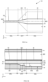
- FIG. 1A is a plan view showing a part of a high frequency circuit in accordance with a first embodiment of the present disclosure
- FIG. 1B is a side sectional view showing a part of the high frequency circuit in accordance with a first embodiment of the present disclosure
- FIG. 1B is a sectional view of a plane parallel to the transmission direction of a high-frequency signal.
- FIGS. 2A and 2B are sectional views of a high-frequency circuit in accordance with a first embodiment of the present disclosure.
- FIG. 2A and FIG. 2B are cross-sectional views of a surface orthogonal to the transmission direction of the high-frequency signal.
- FIG. 2A is a cross-sectional view of a portion of the microstrip line
- FIG. 2B is a cross-sectional view of a portion of the suspended line.
- the high-frequency circuit (10) includes a dielectric substrate (20), a first signal conductor (31), a second signal conductor (32), a signal conductor (connected conductor) (300, 300A), a ground conductor (41), a metal housing (81), and a metal housing (82).
- the dielectric substrate (20) is a substrate having a predetermined dielectric constant.
- the dielectric substrate (20) is, for example, a substrate such as FR-4 using a glass epoxy resin.
- the dielectric substrate (20) is a flat plate having a first surface (201) and a second surface (202) facing each other and having a constant thickness.
- the first signal conductor (31), the second signal conductor (32), and the signal conductor (300) are arranged on the first surface (201) of the dielectric substrate (20).
- the first signal conductor (31) and the second signal conductor (32) are connected through the signal conductor (300).
- the first signal conductor (31) is a linear (band-like) flat film conductor having a width W31.
- the second signal conductor (32) is a linear (band-like) flat film conductor having a width W32.
- the width W31 of the first signal conductor (31) is narrower than the width W32 of the second signal conductor (32). In other words, the width W32 of the second signal conductor (32) is wider than the width W31 of the first signal conductor (31).
- the signal conductor (300) has a first end connected to the first signal conductor (31) and a second end connected to the second signal conductor (32).
- the signal conductor (300) is a linear (banded) flat film conductor whose width varies between the first end and the second end.
- the signal conductor (300) has a shape that increases in width from the first end to the second end and may also have a shape that increases in width gradually.
- the width of the signal conductor (300) increases continuously.
- the signal conductor (300) has no place where the width varies discretely between the first end and the second end.
- the width at the first end of the signal conductor (300) is the same as the width W31 of the first signal conductor (31).
- the width at the second end of the signal conductor (300) is the same as the width W32 of the second signal conductor (32).
- the ground conductor (41) is disposed on the second surface (202) of the dielectric substrate (20).
- the ground conductor (41) is a flat film conductor.
- the ground conductor (41) overlaps the first signal conductor (31) in plan view (in the z-axis direction of the figure) and does not overlap the signal conductors (300) and (32).
- the width of the ground conductor (41) is wider than the width W31 of the first signal conductor (31). Specifically, the width of the ground conductor (41) is wide enough to have little adverse effect on the electric field formation and transmission characteristics of the microstrip line (MSL), which will be described later, as a high-frequency circuit (10).
- MSL microstrip line
- the metal housing (81) is disposed on the side of the first surface (201) of the dielectric substrate (20) through the upper cavity (800).
- the height of the upper cavity (800) is such that the first signal conductor (31), the second signal conductor (32), the signal conductor (300), and the metal housing (81) are hardly electromagnetically coupled.
- the metal housing (82) is arranged on the side of the second surface (202) of the dielectric substrate (20).
- the metal housing (82) has a first portion overlapping the first signal conductor (31), a second portion overlapping the second signal conductor (32), and a third portion overlapping the signal conductor (300) in a plane view in the direction (x-axis direction in the figure) in which the first signal conductor (31), the signal conductor (300), and the second signal conductor (32) are connected.
- the height of the first portion is higher than the height of the second portion.
- the height of the third portion gradually decreases from the end connected to the first portion to the end connected to the second portion. At this time, the height of the third portion is continuously lowered.
- the third portion has no portion where the height varies discretely between the end portion connected to the first portion and the end portion connected to the second portion.
- the metal housing (82) is arranged such that the main surface (821) of the first portion abuts the ground conductor (41).
- a lower cavity (50) is formed between the main surface (822) of the second portion of the metal housing (82) and the second surface (202) of the dielectric substrate (20).
- a lower cavity (53) is formed between the main surface (823) of the third portion of the metal housing (82) and the second surface (202) of the dielectric substrate (20).
- the lower cavity (50) communicates with the lower cavity (53).
- the metal housing (82) may play the role of the ground conductor (41).
- the height H50 (the distance in the height direction (z-axis direction) between the main surface (822) and the second surface (202) of the lower cavity (50) is constant.
- the width of the lower cavity (50) is wider than the width of the second signal conductor (32) and is wide enough to have little adverse effect on the electric field formation and transmission characteristics of the suspended-line (SML) described later as the high-frequency circuit (10).
- the height H53 (the distance in the height direction (z-axis direction) between the main surface (823) and the second surface (202) of the lower cavity (53) gradually increases from the end portion on the side of the first signal conductor (31) toward the end portion on the side of the second signal conductor (32) because the metal housing (82) has the above-mentioned shape. At this time, the height H53 is continuously increased.
- the height H53 of the lower cavity (53) is the same as the height H50 of the lower cavity (50) at the end portion communicating with the lower cavity (50).
- the width of the lower cavity (53) gradually increases from the end portion on the side of the first signal conductor (31) toward the end portion on the side of the second signal conductor (32).
- the width of the lower cavity (53) is the same as the width of the lower cavity (50) at the end portion communicating with the lower cavity (50).
- the high-frequency circuit (10) includes a microstrip line (MSL), a suspended line (SML), and a connector (MTP).
- MSL microstrip line
- SML suspended line
- MTP connector
- the microstrip line (MSL) is formed of the first signal conductor (31), a dielectric substrate (20), and a ground conductor (41).
- the suspended line (SML) is formed of the second signal conductor (32), a dielectric substrate (20), a lower cavity (50), and a metal housing (82).
- the connector (MTP) is formed of a signal conductor (300), a dielectric substrate (20), a lower cavity (53), and a metal housing (82).
- the width W31 of the first signal conductor (31) of the microstrip line (MSL) is narrower than the width W32 of the second signal conductor (32) of the suspended line (SML).
- the high-frequency circuit (10) can make the characteristic impedance of the suspended line (SML) having the lower cavity (50) (air layer) between the second signal conductor (32) and the metal housing (82) the same as the characteristic impedance of the microstrip line (MSL).
- the transmission loss of the high-frequency circuit (10) can be reduced compared with using the microstrip line (MSL) alone.
- MSL microstrip line
- the transmission loss of the high-frequency circuit (10) can be effectively reduced by using the suspended line (SML).
- the height H50 of the lower cavity (50) is preferably larger than the thickness of the dielectric substrate (20).
- the high-frequency circuit (10) can further suppress the transmission loss in the suspended line (SML).
- the width of the signal conductor (300) of the connector MTP gradually increases from the first end on the microstrip line (MSL) side to the second end on the suspended line (SML) side.
- the high-frequency circuit (10) can suppress the connection loss between the microstrip line (MSL) and the suspended line (SML).
- the height H53 of the lower cavity (53) of the connector MTP gradually increases from the first end of the microstrip line (MSL) side to the second end of the suspended line (SML) side.
- the electric field distribution and the transmission mode do not suddenly change in the connector MTP, but gradually change. Therefore, the high-frequency circuit (10) can suppress the loss in the connector MTP.
- the width of the lower cavity (53) of the connector MTP gradually increases from the first end of the microstrip line (MSL) side to the second end of the suspended line (SML) side.
- the width of the lower cavity (53) of the connector MTP may be equal to or greater than the width of the second signal conductor (32) of the suspended line.
- FIG. 3A is a side sectional view schematically showing the electric field distribution of the high-frequency circuit of the present disclosure
- FIG. 3B is a side sectional view schematically showing the electric field distribution of the high-frequency circuit of the comparative configuration in accordance with an embodiment of the present disclosure.
- FIG. 4A is a graph showing S 1 1 characteristics between the high-frequency circuit of the present disclosure and the high-frequency circuit of the comparative configuration
- FIG. 4B is a graph showing S21 characteristics between the high-frequency circuit of the present disclosure and the high-frequency circuit of the comparative configuration.
- solid lines indicate S11 characteristics and S21 characteristics of the high-frequency circuit of the present disclosure
- dashed lines indicate S11 characteristics and S21 characteristics of the high-frequency circuit of the comparative configuration.
- the comparative configuration is a configuration in which the microstrip line (MSL) and the suspended line (SML) are directly connected without the connector MTP of the present disclosure.
- the high-frequency circuit (10) of the present disclosure can suppress the sudden change of the electric field distribution as in the comparative configuration at the point where the microstrip line (MSL) and the suspended line (SML) are connected.
- the high-frequency circuit (10) of the present disclosure can realize superior S11 characteristics and superior S21 characteristics than the comparative configuration and can reduce the loss at the point where the microstrip line (MSL) and the suspended line (SML) are connected.
- the high-frequency circuit 10 of this configuration is applied to the radar (90), for example.
- FIG. 5A is a plan view showing a part of the radar (90) apparatus
- FIG. 5B is a side sectional view showing a part of the radar (90) apparatus in accordance with an embodiment of the present disclosure.
- the radar (90) apparatus includes a high-frequency circuit (10) and a high-frequency element (91).
- the high-frequency element (91) is, for example, a high-power amplifier or the like, and is, for example, an element used in a transmission circuit or a reception circuit of a radar (90).
- the high-frequency element (91) is not limited thereto, but also includes a passive element such as a capacitor.
- the high-frequency element (91) is mounted on terminal conductors (311) and (312) connected to the first signal conductor (31) in the microstrip line (MSL).
- the high-frequency element (91) has a ground terminal, which is mounted on a terminal conductor (313) formed on the first surface (201) of the dielectric substrate (20).
- the terminal conductor (313) is connected to the ground conductor (41) through a via conductor formed on the dielectric substrate (20).
- the radar (90) mounts the high-frequency element (91) with the ground terminal at the location of the microstrip line (MSL).
- the radar (90) can reliably and easily mount the high-frequency element (91) with the ground terminal in the high-frequency circuit (10).
- the radar (90) uses a suspended line (SML) in a part where the high-frequency element (91) is not mounted.
- SML suspended line
- the radar (90) can suppress the transmission loss and realize a highly efficient radar.
- the portion using the suspended line (SML) is preferably longer than the portion using the microstrip line (MSL).
- MSL microstrip line
- the radar (90) is shown as an example in the present embodiment, the above-described configuration of the high-frequency circuit (10) can be adopted in the case of a high-frequency device in which electronic components are mounted.
- the loss of the high-frequency device can be reduced, and the characteristics of the high-frequency device can be improved.
- the metal casing (81) and the metal casing (82) are fixed across the dielectric substrate (20) so as to include the dielectric substrate (20), the first signal conductor (31), the second signal conductor (32), the signal conductor (300), and the ground conductor (41).
- the electromagnetic field coupling between the metal casing (81) and the metal casing (82), the microstrip line (MSL), the suspended line (SML), and the connector MTP which will be described later, and the outside of the metal casing (81) and the metal casing (82) can be suppressed.
- the metal casing (82) is used for the metal layer coupled to the second signal conductor (32) in the suspended line (SML), and for the metal layer coupled to the signal conductor (300) in the connector MTP.
- an electrode film metal film
- an electrode film may be formed on a dielectric substrate different from the dielectric substrate (20), and the electrode film (metal film) may be used as a metal layer.
- the high-frequency circuit (10) can be realized in a simple configuration.
- the height of the lower cavity (50) of the suspended line (SML) and the height of the lower cavity (53) of the connector MTP can be set without affecting the shape of the metal housing (82).
- FIG. 6A is a plan view showing a part of a high-frequency circuit according to a second embodiment of the present disclosure
- FIG. 6B is a side sectional view showing a part of a high-frequency circuit in accordance with a second embodiment of the present disclosure.
- the high-frequency circuit (10A) according to the second embodiment is different from the high-frequency circuit (10) according to the first embodiment in that it has a connector MTPA.
- the other configuration of the high-frequency circuit (10A) is the same as that of the high-frequency circuit (10), and the description of the similar elements will be omitted.
- the high-frequency circuit (10A) includes a connector MTPA.
- the connector MTPA includes a signal conductor (300A), a metal housing (82A), and a lower cavity (53A).
- the width of the signal conductor (300A) varies discretely (stepwise) from the first end connecting to the first signal conductor (31) to the second end connecting to the second signal conductor (32).
- the height of the third portion of the metal housing (82A) decreases discretely from the end on the side of the first signal conductor (31) toward the end on the side of the second signal conductor (32). That is, the height H53A of the lower cavity (53A) increases discretely toward the side communicating with the lower cavity (50).
- the width of the lower cavity (53A) is discretely increased toward the side communicating with the lower cavity (50).
- the high-frequency circuit (10A) can suppress the connection loss between the microstrip line (MSL) and the suspended line (SML) as well as the high-frequency circuit (10).
- Various embodiments of the present disclosure provides a high-frequency circuit that includes a microstrip line, a suspended line, and a connector.
- the high-frequency circuit enables several advantages as listed below:
Landscapes
- Engineering & Computer Science (AREA)
- Radar, Positioning & Navigation (AREA)
- Remote Sensing (AREA)
- Physics & Mathematics (AREA)
- Computer Networks & Wireless Communication (AREA)
- General Physics & Mathematics (AREA)
- Electromagnetism (AREA)
- Waveguides (AREA)
- Waveguide Connection Structure (AREA)
Abstract
Description
- Embodiments of the present disclosure relate to the field of electronic circuits, and more particularly, to a high-frequency circuit provided with a transmission line in which a microstrip line and a suspended line are connected.
- Patent Literature 1 describes a transmission line in which a microstrip line and a suspended line are connected. However, the loss is large at the connector between the microstrip line and the suspended line.
- Patent Literature 1:
Japanese Patent Publication No. 2014-220628 - Hence, there is a need for an improved system to reduce the loss at the connector between the microstrip line and the suspended line which addresses the aforementioned issue(s).
- An objective of the present disclosure is to reduce the loss at the connector between a microstrip line and a suspended line.
- In accordance with an embodiment of the present disclosure, a high-frequency circuit is provided. The high-frequency circuit includes a microstrip line. The microstrip line includes a dielectric substrate having a first surface and a second surface opposed to each other. Further, the microstrip line includes a first signal conductor disposed on the first surface and a ground conductor disposed on the second surface. The high-frequency circuit also includes a suspended line. The suspended line includes the dielectric substrate, a second signal conductor disposed on the first surface and a metal layer disposed from the second surface through the first cavity. The high-frequency circuit further includes a connector. The connector includes the dielectric substrate, a connected conductor connecting the first signal conductor to the second signal conductor and a metal layer disposed from the second surface through the second cavity. the connected conductor is designed to widen from a first end connecting to the first signal conductor toward a second end connecting the connected conductor to the second signal conductor. the distance between the dielectric substrate and the metal layer at the second cavity is designed to gradually increase from the first end toward the second end.
- In accordance with an embodiment of the present disclosure, a radar is provided. The radar includes a high-frequency circuit. Further, the radar includes a high-frequency element for the radar to be mounted on the microstrip line of the high-frequency circuit.
- To further clarify the advantages and features of the present disclosure, a more particular description of the disclosure will follow by reference to specific embodiments thereof, which are illustrated in the appended figures. It is to be appreciated that these figures depict only typical embodiments of the disclosure and are therefore not to be considered limiting in scope. The disclosure will be described and explained with additional specificity and detail with the appended figures.
- The disclosure will be described and explained with additional specificity and detail with the accompanying figures in which:
-
FIG. 1A is a plan view showing a part of a high frequency circuit according to a first embodiment of the present disclosure, andFIG. 1B is a side sectional view showing a part of a high frequency circuit in accordance with a first embodiment of the present disclosure; -
FIG. 2A and FIG. 2B are sectional views of a high frequency circuit in accordance with the first embodiment of the present disclosure; -
FIG. 3A is a side sectional view schematically showing an electric field distribution of a high frequency circuit of the present disclosure, andFIG. 3B is a side sectional view schematically showing an electric field distribution of a high frequency circuit in a comparative configuration in accordance with an embodiment of the present disclosure; -
FIG. 4A is a graph showing S11 characteristics between a high frequency circuit of the present disclosure and a high frequency circuit in a comparative configuration, andFIG. 4B is a graph showing S21 characteristics between a high frequency circuit of the present disclosure and a high frequency circuit in a comparative configuration in accordance with an embodiment of the present disclosure; -
FIG. 5A is a plan view showing a part of the radar apparatus, andFIG. 5B is a side sectional view showing a part of the radar apparatus in accordance with an embodiment of the present disclosure; and -
FIG. 6A is a plan view showing a part of the high frequency circuit according to a second embodiment of the present disclosure, andFIG. 6B is a side sectional view showing a part of the high frequency circuit in accordance with a second embodiment of the present disclosure. - Further, those skilled in the art will appreciate that elements in the figures are illustrated for simplicity and may not have necessarily been drawn to scale. Furthermore, in terms of the construction of the device, one or more components of the device may have been represented in the figures by conventional symbols, and the figures may show only those specific details that are pertinent to understanding the embodiments of the present disclosure so as not to obscure the figures with details that will be readily apparent to those skilled in the art having the benefit of the description herein.
- For the purpose of promoting an understanding of the principles of the disclosure, reference will now be made to the embodiment illustrated in the figures and specific language will be used to describe them. It will nevertheless be understood that no limitation of the scope of the disclosure is thereby intended. Such alterations and further modifications in the illustrated system, and such further applications of the principles of the disclosure as would normally occur to those skilled in the art are to be construed as being within the scope of the present disclosure.
- The terms "comprises", "comprising", or any other variations thereof, are intended to cover a non-exclusive inclusion, such that a process or method that comprises a list of steps does not include only those steps but may include other steps not expressly listed or inherent to such a process or method. Similarly, one or more devices or subsystems or elements or structures or components preceded by "comprises... a" does not, without more constraints, preclude the existence of other devices, sub-systems, elements, structures, components, additional devices, additional sub-systems, additional elements, additional structures or additional components. Appearances of the phrase "in an embodiment", "in another embodiment" and similar language throughout this specification may, but not necessarily do, all refer to the same embodiment.
- Unless otherwise defined, all technical and scientific terms used herein have the same meaning as commonly understood by those skilled in the art to which this disclosure belongs. The system, methods, and examples provided herein are only illustrative and not intended to be limiting.
- In the following specification and the claims, reference will be made to a number of terms, which shall be defined to have the following meanings. The singular forms "a", "an", and "the" include plural references unless the context clearly dictates otherwise.
- In accordance with an embodiment of the present disclosure, a high-frequency circuit is provided. The high-frequency circuit includes a microstrip line. The microstrip line includes a dielectric substrate having a first surface and a second surface opposed to each other. Further, the microstrip line includes a first signal conductor disposed on the first surface and a ground conductor disposed on the second surface. The high-frequency circuit also includes a suspended line. The suspended line includes the dielectric substrate, a second signal conductor disposed on the first surface and a metal layer disposed from the second surface through the first cavity. The high-frequency circuit further includes a connector. The connector includes the dielectric substrate, a connected conductor connecting the first signal conductor to the second signal conductor and a metal layer disposed from the second surface through the second cavity. the connected conductor is designed to widen from a first end connecting to the first signal conductor toward a second end connecting the connected conductor to the second signal conductor. the distance between the dielectric substrate and the metal layer at the second cavity is designed to gradually increase from the first end toward the second end.
-
FIG. 1A is a plan view showing a part of a high frequency circuit in accordance with a first embodiment of the present disclosure, andFIG. 1B is a side sectional view showing a part of the high frequency circuit in accordance with a first embodiment of the present disclosure.FIG. 1B is a sectional view of a plane parallel to the transmission direction of a high-frequency signal. -
FIGS. 2A and 2B are sectional views of a high-frequency circuit in accordance with a first embodiment of the present disclosure.FIG. 2A and FIG. 2B are cross-sectional views of a surface orthogonal to the transmission direction of the high-frequency signal.FIG. 2A is a cross-sectional view of a portion of the microstrip line, andFIG. 2B is a cross-sectional view of a portion of the suspended line. - As shown in
FIG. 1A, FIG. 1B ,FIG. 2A, and FIG. 2B , the high-frequency circuit (10) includes a dielectric substrate (20), a first signal conductor (31), a second signal conductor (32), a signal conductor (connected conductor) (300, 300A), a ground conductor (41), a metal housing (81), and a metal housing (82). - The dielectric substrate (20) is a substrate having a predetermined dielectric constant. The dielectric substrate (20) is, for example, a substrate such as FR-4 using a glass epoxy resin. The dielectric substrate (20) is a flat plate having a first surface (201) and a second surface (202) facing each other and having a constant thickness.
- The first signal conductor (31), the second signal conductor (32), and the signal conductor (300) are arranged on the first surface (201) of the dielectric substrate (20). The first signal conductor (31) and the second signal conductor (32) are connected through the signal conductor (300).
- The first signal conductor (31) is a linear (band-like) flat film conductor having a width W31. The second signal conductor (32) is a linear (band-like) flat film conductor having a width W32. The width W31 of the first signal conductor (31) is narrower than the width W32 of the second signal conductor (32). In other words, the width W32 of the second signal conductor (32) is wider than the width W31 of the first signal conductor (31).
- The signal conductor (300) has a first end connected to the first signal conductor (31) and a second end connected to the second signal conductor (32). The signal conductor (300) is a linear (banded) flat film conductor whose width varies between the first end and the second end. The signal conductor (300) has a shape that increases in width from the first end to the second end and may also have a shape that increases in width gradually.
- At this time, the width of the signal conductor (300) increases continuously. In other words, the signal conductor (300) has no place where the width varies discretely between the first end and the second end.
- The width at the first end of the signal conductor (300) is the same as the width W31 of the first signal conductor (31). The width at the second end of the signal conductor (300) is the same as the width W32 of the second signal conductor (32).
- The ground conductor (41) is disposed on the second surface (202) of the dielectric substrate (20). The ground conductor (41) is a flat film conductor. The ground conductor (41) overlaps the first signal conductor (31) in plan view (in the z-axis direction of the figure) and does not overlap the signal conductors (300) and (32).
- The width of the ground conductor (41) is wider than the width W31 of the first signal conductor (31). Specifically, the width of the ground conductor (41) is wide enough to have little adverse effect on the electric field formation and transmission characteristics of the microstrip line (MSL), which will be described later, as a high-frequency circuit (10).
- The metal housing (81) is disposed on the side of the first surface (201) of the dielectric substrate (20) through the upper cavity (800). The height of the upper cavity (800) is such that the first signal conductor (31), the second signal conductor (32), the signal conductor (300), and the metal housing (81) are hardly electromagnetically coupled.
- The metal housing (82) is arranged on the side of the second surface (202) of the dielectric substrate (20). The metal housing (82) has a first portion overlapping the first signal conductor (31), a second portion overlapping the second signal conductor (32), and a third portion overlapping the signal conductor (300) in a plane view in the direction (x-axis direction in the figure) in which the first signal conductor (31), the signal conductor (300), and the second signal conductor (32) are connected.
- The height of the first portion is higher than the height of the second portion. The height of the third portion gradually decreases from the end connected to the first portion to the end connected to the second portion. At this time, the height of the third portion is continuously lowered. In other words, the third portion has no portion where the height varies discretely between the end portion connected to the first portion and the end portion connected to the second portion.
- The metal housing (82) is arranged such that the main surface (821) of the first portion abuts the ground conductor (41). Thus, a lower cavity (50) is formed between the main surface (822) of the second portion of the metal housing (82) and the second surface (202) of the dielectric substrate (20). A lower cavity (53) is formed between the main surface (823) of the third portion of the metal housing (82) and the second surface (202) of the dielectric substrate (20). The lower cavity (50) communicates with the lower cavity (53). In the microstrip line, the metal housing (82) may play the role of the ground conductor (41).
- The height H50 (the distance in the height direction (z-axis direction) between the main surface (822) and the second surface (202) of the lower cavity (50) is constant. The width of the lower cavity (50) is wider than the width of the second signal conductor (32) and is wide enough to have little adverse effect on the electric field formation and transmission characteristics of the suspended-line (SML) described later as the high-frequency circuit (10).
- The height H53 (the distance in the height direction (z-axis direction) between the main surface (823) and the second surface (202) of the lower cavity (53) gradually increases from the end portion on the side of the first signal conductor (31) toward the end portion on the side of the second signal conductor (32) because the metal housing (82) has the above-mentioned shape. At this time, the height H53 is continuously increased. The height H53 of the lower cavity (53) is the same as the height H50 of the lower cavity (50) at the end portion communicating with the lower cavity (50).
- The width of the lower cavity (53) gradually increases from the end portion on the side of the first signal conductor (31) toward the end portion on the side of the second signal conductor (32). The width of the lower cavity (53) is the same as the width of the lower cavity (50) at the end portion communicating with the lower cavity (50).
- With this configuration, the high-frequency circuit (10) includes a microstrip line (MSL), a suspended line (SML), and a connector (MTP).
- The microstrip line (MSL) is formed of the first signal conductor (31), a dielectric substrate (20), and a ground conductor (41).
- The suspended line (SML) is formed of the second signal conductor (32), a dielectric substrate (20), a lower cavity (50), and a metal housing (82).
- The connector (MTP) is formed of a signal conductor (300), a dielectric substrate (20), a lower cavity (53), and a metal housing (82).
- In this configuration, the width W31 of the first signal conductor (31) of the microstrip line (MSL) is narrower than the width W32 of the second signal conductor (32) of the suspended line (SML). As a result, the high-frequency circuit (10) can make the characteristic impedance of the suspended line (SML) having the lower cavity (50) (air layer) between the second signal conductor (32) and the metal housing (82) the same as the characteristic impedance of the microstrip line (MSL).
- By using the suspended line (SML), the transmission loss of the high-frequency circuit (10) can be reduced compared with using the microstrip line (MSL) alone. In particular, when the frequency of the high-frequency signal is high, the loss becomes larger when a general-purpose and inexpensive dielectric substrate (20) such as FR-4 is used, but the transmission loss of the high-frequency circuit (10) can be effectively reduced by using the suspended line (SML).
- In this case, the height H50 of the lower cavity (50) is preferably larger than the thickness of the dielectric substrate (20). Thus, the high-frequency circuit (10) can further suppress the transmission loss in the suspended line (SML).
- In the high-frequency circuit (10), the width of the signal conductor (300) of the connector MTP gradually increases from the first end on the microstrip line (MSL) side to the second end on the suspended line (SML) side. As a result, the electric field distribution and the transmission mode do not suddenly change in the connector MTP, but gradually change. Therefore, the high-frequency circuit (10) can suppress the connection loss between the microstrip line (MSL) and the suspended line (SML).
- Furthermore, in the high-frequency circuit (10), the height H53 of the lower cavity (53) of the connector MTP gradually increases from the first end of the microstrip line (MSL) side to the second end of the suspended line (SML) side. As a result, the electric field distribution and the transmission mode do not suddenly change in the connector MTP, but gradually change. Therefore, the high-frequency circuit (10) can suppress the loss in the connector MTP.
- Further, in the high-frequency circuit (10), the width of the lower cavity (53) of the connector MTP gradually increases from the first end of the microstrip line (MSL) side to the second end of the suspended line (SML) side. As a result, the electric field distribution and the transmission mode do not suddenly change in the connector MTP, but gradually change. Therefore, the high-frequency circuit (10) can suppress the loss in the connector MTP. The width of the lower cavity (53) of the connector MTP may be equal to or greater than the width of the second signal conductor (32) of the suspended line.
-
FIG. 3A is a side sectional view schematically showing the electric field distribution of the high-frequency circuit of the present disclosure, andFIG. 3B is a side sectional view schematically showing the electric field distribution of the high-frequency circuit of the comparative configuration in accordance with an embodiment of the present disclosure. -
FIG. 4A is a graph showing S 1 1 characteristics between the high-frequency circuit of the present disclosure and the high-frequency circuit of the comparative configuration, andFIG. 4B is a graph showing S21 characteristics between the high-frequency circuit of the present disclosure and the high-frequency circuit of the comparative configuration. InFIGs. 4(A) and 4(B) , solid lines indicate S11 characteristics and S21 characteristics of the high-frequency circuit of the present disclosure, while dashed lines indicate S11 characteristics and S21 characteristics of the high-frequency circuit of the comparative configuration. - The comparative configuration is a configuration in which the microstrip line (MSL) and the suspended line (SML) are directly connected without the connector MTP of the present disclosure.
- As shown in
FIGS. 3(A) and 3(B) , the high-frequency circuit (10) of the present disclosure can suppress the sudden change of the electric field distribution as in the comparative configuration at the point where the microstrip line (MSL) and the suspended line (SML) are connected. - As a result, the high-frequency circuit (10) of the present disclosure can realize superior S11 characteristics and superior S21 characteristics than the comparative configuration and can reduce the loss at the point where the microstrip line (MSL) and the suspended line (SML) are connected.
- The high-
frequency circuit 10 of this configuration is applied to the radar (90), for example. -
FIG. 5A is a plan view showing a part of the radar (90) apparatus, andFIG. 5B is a side sectional view showing a part of the radar (90) apparatus in accordance with an embodiment of the present disclosure. - As shown in
FIG. 5A , the radar (90) apparatus includes a high-frequency circuit (10) and a high-frequency element (91). The high-frequency element (91) is, for example, a high-power amplifier or the like, and is, for example, an element used in a transmission circuit or a reception circuit of a radar (90). The high-frequency element (91) is not limited thereto, but also includes a passive element such as a capacitor. - The high-frequency element (91) is mounted on terminal conductors (311) and (312) connected to the first signal conductor (31) in the microstrip line (MSL). The high-frequency element (91) has a ground terminal, which is mounted on a terminal conductor (313) formed on the first surface (201) of the dielectric substrate (20). The terminal conductor (313) is connected to the ground conductor (41) through a via conductor formed on the dielectric substrate (20).
- Thus, the radar (90) mounts the high-frequency element (91) with the ground terminal at the location of the microstrip line (MSL). Thus, the radar (90) can reliably and easily mount the high-frequency element (91) with the ground terminal in the high-frequency circuit (10).
- In addition, the radar (90) uses a suspended line (SML) in a part where the high-frequency element (91) is not mounted. Thus, the radar (90) can suppress the transmission loss and realize a highly efficient radar. In this case, the portion using the suspended line (SML) is preferably longer than the portion using the microstrip line (MSL). As a result, the radar (90) can further suppress transmission loss and realize a highly efficient radar.
- Although the radar (90) is shown as an example in the present embodiment, the above-described configuration of the high-frequency circuit (10) can be adopted in the case of a high-frequency device in which electronic components are mounted. Thus, the loss of the high-frequency device can be reduced, and the characteristics of the high-frequency device can be improved.
- Although not shown, the metal casing (81) and the metal casing (82) are fixed across the dielectric substrate (20) so as to include the dielectric substrate (20), the first signal conductor (31), the second signal conductor (32), the signal conductor (300), and the ground conductor (41). Thus, the electromagnetic field coupling between the metal casing (81) and the metal casing (82), the microstrip line (MSL), the suspended line (SML), and the connector MTP, which will be described later, and the outside of the metal casing (81) and the metal casing (82) can be suppressed.
- In the above description, the metal casing (82) is used for the metal layer coupled to the second signal conductor (32) in the suspended line (SML), and for the metal layer coupled to the signal conductor (300) in the connector MTP. However, for example, an electrode film (metal film) may be formed on a dielectric substrate different from the dielectric substrate (20), and the electrode film (metal film) may be used as a metal layer.
- By using the metal housing (82) as a metal layer, the high-frequency circuit (10) can be realized in a simple configuration. On the other hand, by separately providing the dielectric substrate (20), the height of the lower cavity (50) of the suspended line (SML) and the height of the lower cavity (53) of the connector MTP can be set without affecting the shape of the metal housing (82).
- A high-frequency circuit according to a second embodiment of the present disclosure will be described with reference to the figure.
FIG. 6A is a plan view showing a part of a high-frequency circuit according to a second embodiment of the present disclosure, andFIG. 6B is a side sectional view showing a part of a high-frequency circuit in accordance with a second embodiment of the present disclosure. - As shown in
FIGS. 6A and 6B , the high-frequency circuit (10A) according to the second embodiment is different from the high-frequency circuit (10) according to the first embodiment in that it has a connector MTPA. The other configuration of the high-frequency circuit (10A) is the same as that of the high-frequency circuit (10), and the description of the similar elements will be omitted. - The high-frequency circuit (10A) includes a connector MTPA. The connector MTPA includes a signal conductor (300A), a metal housing (82A), and a lower cavity (53A).
- The width of the signal conductor (300A) varies discretely (stepwise) from the first end connecting to the first signal conductor (31) to the second end connecting to the second signal conductor (32).
- The height of the third portion of the metal housing (82A) decreases discretely from the end on the side of the first signal conductor (31) toward the end on the side of the second signal conductor (32). That is, the height H53A of the lower cavity (53A) increases discretely toward the side communicating with the lower cavity (50).
- The width of the lower cavity (53A) is discretely increased toward the side communicating with the lower cavity (50).
- With such a configuration, the high-frequency circuit (10A) can suppress the connection loss between the microstrip line (MSL) and the suspended line (SML) as well as the high-frequency circuit (10).
- Various embodiments of the present disclosure provides a high-frequency circuit that includes a microstrip line, a suspended line, and a connector. The high-frequency circuit enables several advantages as listed below:
- 1. The transmission mode gradually changes from the microstrip line to the suspended line or from the suspended line to the microstrip line. This reduces the transmission loss between the microstrip line and the suspended line.
- 2. The width of the connected conductor is designed to vary continuously, and to be the width of the first signal conductor at the first end and the width of the second signal conductor at the second end. In this configuration, transmission loss can be further suppressed.
- 3. The width of the connected conductor is designed to vary gradually and discretely, and to be the width of the first signal conductor at the first end and the width of the second signal conductor at the second end. In this configuration, manufacturing is made easier while realizing a predetermined transmission loss.
- 4. The distance between the dielectric substrate and the metal layer at the second cavity is designed to vary continuously, and to be the distance between the dielectric substrate and the metal layer at the first cavity at the second end. In this configuration, transmission loss can be further suppressed.
- 5. The dielectric substrate and the metal layer at the second cavity is designed to vary discretely, and to be the distance between the dielectric substrate and the metal layer at the first cavity at the second end. In this configuration, manufacturing is made easier while realizing a predetermined transmission loss.
- 6. The metal layer is a metal housing surrounding the microstrip line and the suspended line. In this configuration, the metal housing surrounding the high-frequency circuit and shielding it electromagnetically can be used for the suspended line and the connector.
- 7. The metal layer is a metal film formed on an insulator. In this configuration, the shape of the suspended line and the connector can be realized separately from the metal housing, and the design freedom of the suspended line and the connector can be improved.
- 8. The radar is mounted on a microstrip line of the high frequency circuit. In this configuration, a low loss radar can be realized. In particular, a low loss radar can be realized while using an inexpensive dielectric substrate.
- It will be understood by those skilled in the art that the foregoing general description and the following detailed description are exemplary and explanatory of the disclosure and are not intended to be restrictive thereof.
- While specific language has been used to describe the disclosure, any limitations arising on account of the same are not intended. As would be apparent to a person skilled in the art, various working modifications may be made to the method in order to implement the inventive concept as taught herein.
- The figures and the foregoing description give examples of embodiments. Those skilled in the art will appreciate that one or more of the described elements may well be combined into a single functional element. Alternatively, certain elements may be split into multiple functional elements. Elements from one embodiment may be added to another embodiment. For example, the order of processes described herein may be changed and are not limited to the manner described herein. Moreover, the actions of any flow diagram need not be implemented in the order shown; nor do all of the acts need to be necessarily performed. Also, those acts that are not dependent on other acts may be performed in parallel with the other acts. The scope of embodiments is by no means limited by these specific examples.
Claims (8)
- A high-frequency circuit (10) comprising:a microstrip line (MSL) comprising:a dielectric substrate (20) having a first surface (201) and a second surface (202) opposed to each other;a first signal conductor (31) disposed on the first surface (201); anda ground conductor (41) disposed on the second surface (202);a suspended line (SML) comprising:the dielectric substrate (20);a second signal conductor (32) disposed on the first surface (201); anda metal layer (82, 82A) disposed from the second surface (202) through the first cavity (50); anda connector (MTP, MTPA) comprising:the dielectric substrate (20);a connected conductor (300,300A) connecting the first signal conductor (31) to the second signal conductor (32); andthe metal layer (82, 82A) disposed from the second surface (202) through the second cavity (53, 53A); wherein:the connected conductor (300, 300A) is designed to widen from a first end connecting to the first signal conductor (31) toward a second end connecting the connected conductor (300,300A) to the second signal conductor (32); andthe distance between the dielectric substrate (20) and the metal layer at the second cavity (53, 53A) is designed to gradually increase from the first end toward the second end.
- The high-frequency circuit (10) of claim 1, wherein the width of the connected conductor (300, 300A) is designed:to vary continuously; andto be the width of the first signal conductor (31) at the first end and the width of the second signal conductor (32) at the second end.
- The high-frequency circuit (10) of claim 1, wherein the width of the connected conductor (300, 300A) is designed:to vary gradually and discretely; andto be the width of the first signal conductor (31) at the first end and the width of the second signal conductor (32) at the second end.
- The high-frequency circuit (10) of claim 1, wherein the distance between the dielectric substrate (20) and the metal layer at the second cavity is designed:to vary continuously; andto be the distance between the dielectric substrate (20) and the metal layer at the first cavity at the second end.
- The high-frequency circuit (10) of claim 1, wherein the distance between the dielectric substrate (20) and the metal layer at the second cavity is designed:to vary discretely; andto be the distance between the dielectric substrate (20) and the metal layer at the first cavity at the second end.
- The high-frequency circuit (10) of claim 1, wherein the metal layer is a metal enclosure surrounding the microstrip line and the suspended line.
- The high-frequency circuit (10) of claim 1, wherein the metal layer is a metal film formed on an insulator.
- A radar (90) comprising:a high-frequency circuit according to claims 1 to 7; anda high-frequency element for the radar (90) to be mounted on the microstrip line of the high-frequency circuit.
Applications Claiming Priority (1)
| Application Number | Priority Date | Filing Date | Title |
|---|---|---|---|
| JP2022172395A JP2024064072A (en) | 2022-10-27 | 2022-10-27 | High frequency circuit and radar device |
Publications (1)
| Publication Number | Publication Date |
|---|---|
| EP4362217A1 true EP4362217A1 (en) | 2024-05-01 |
Family
ID=88511504
Family Applications (1)
| Application Number | Title | Priority Date | Filing Date |
|---|---|---|---|
| EP23205213.4A Pending EP4362217A1 (en) | 2022-10-27 | 2023-10-23 | High frequency circuit and radar device |
Country Status (4)
| Country | Link |
|---|---|
| US (1) | US12578423B2 (en) |
| EP (1) | EP4362217A1 (en) |
| JP (1) | JP2024064072A (en) |
| CN (1) | CN117954817A (en) |
Citations (4)
| Publication number | Priority date | Publication date | Assignee | Title |
|---|---|---|---|---|
| DE4241635C2 (en) * | 1992-12-10 | 1994-11-10 | Ant Nachrichtentech | Transition from a microstrip line to a waveguide |
| US5844450A (en) * | 1996-03-05 | 1998-12-01 | Motorola, Inc. | Integrated microstrip to suspend stripline transition structure and method of fabrication |
| US20110115578A1 (en) * | 2009-11-17 | 2011-05-19 | Clifton Quan | Rf transition with 3-dimensional molded rf structure |
| JP2014220628A (en) | 2013-05-08 | 2014-11-20 | 三菱電機株式会社 | Transmission line |
Family Cites Families (26)
| Publication number | Priority date | Publication date | Assignee | Title |
|---|---|---|---|---|
| US2633493A (en) * | 1946-04-02 | 1953-03-31 | Seymour B Cohn | Broad-band wave guide-to-coaxial line junction |
| US2802991A (en) * | 1955-07-12 | 1957-08-13 | Sperry Rand Corp | Rectangular wave guide to epsilon-guide transition |
| US2979676A (en) * | 1957-10-30 | 1961-04-11 | Research Corp | Waveguide to microstrip transition structure |
| US3146410A (en) * | 1961-01-05 | 1964-08-25 | Sanders Associates Inc | Strip line to ridged waveguide transition having a probe projecting into waveguide through ridge |
| US3932823A (en) * | 1975-04-23 | 1976-01-13 | The United States Of America As Represented By The Secretary Of The Navy | Microstrip to waveguide adapter |
| US4260964A (en) * | 1979-05-07 | 1981-04-07 | The United States Of America As Represented By The Secretary Of The Navy | Printed circuit waveguide to microstrip transition |
| US4588962A (en) * | 1982-05-31 | 1986-05-13 | Fujitsu Limited | Device for distributing and combining microwave electric power |
| US4901040A (en) * | 1989-04-03 | 1990-02-13 | American Telephone And Telegraph Company | Reduced-height waveguide-to-microstrip transition |
| US5262739A (en) * | 1989-05-16 | 1993-11-16 | Cornell Research Foundation, Inc. | Waveguide adaptors |
| US5225797A (en) * | 1992-04-27 | 1993-07-06 | Cornell Research Foundation, Inc. | Dielectric waveguide-to-coplanar transmission line transitions |
| DE19636890C1 (en) * | 1996-09-11 | 1998-02-12 | Bosch Gmbh Robert | Transition from a waveguide to a strip line |
| FI106414B (en) * | 1999-02-02 | 2001-01-31 | Nokia Networks Oy | Bredbandsimpedansadapter |
| FR2849720B1 (en) * | 2003-01-03 | 2005-04-15 | Thomson Licensing Sa | TRANSITION BETWEEN A RECTANGULAR WAVEGUIDE AND A MICRORUBAN LINE |
| GB0302584D0 (en) * | 2003-02-05 | 2003-03-12 | Smiths Group Plc | Microwave transitions and antennas |
| WO2005048314A2 (en) * | 2003-11-12 | 2005-05-26 | Silicon Pipe, Inc. | Tapered dielectric and conductor structures and applications thereof |
| US20080100394A1 (en) * | 2004-06-30 | 2008-05-01 | Emag Technologies, Inc. | Microstrip to Coplanar Waveguide Transition |
| JP4395103B2 (en) * | 2005-06-06 | 2010-01-06 | 富士通株式会社 | Waveguide substrate and high-frequency circuit module |
| US8159316B2 (en) * | 2007-12-28 | 2012-04-17 | Kyocera Corporation | High-frequency transmission line connection structure, circuit board, high-frequency module, and radar device |
| US8022784B2 (en) * | 2008-07-07 | 2011-09-20 | Korea Advanced Institute Of Science And Technology (Kaist) | Planar transmission line-to-waveguide transition apparatus having an embedded bent stub |
| JP5289551B2 (en) * | 2009-02-27 | 2013-09-11 | 三菱電機株式会社 | Waveguide microstrip line converter |
| JP5493801B2 (en) * | 2009-12-14 | 2014-05-14 | 富士通株式会社 | Signal converter and high-frequency circuit module |
| FR3010835B1 (en) * | 2013-09-19 | 2015-09-11 | Inst Mines Telecom Telecom Bretagne | JUNCTION DEVICE BETWEEN A PRINTED TRANSMISSION LINE AND A DIELECTRIC WAVEGUIDE |
| JP6766582B2 (en) | 2016-10-18 | 2020-10-14 | 三菱電機株式会社 | High frequency transmission device |
| US11303004B2 (en) * | 2019-06-10 | 2022-04-12 | Hughes Network Systems, Llc | Microstrip-to-waveguide transition including a substrate integrated waveguide with a 90 degree bend section |
| JP7606087B2 (en) * | 2021-03-15 | 2024-12-25 | 富士通株式会社 | Power Combiner |
| US12265172B2 (en) * | 2022-05-25 | 2025-04-01 | Aptiv Technologies AG | Vertical microstrip-to-waveguide transition |
-
2022
- 2022-10-27 JP JP2022172395A patent/JP2024064072A/en active Pending
-
2023
- 2023-10-18 CN CN202311348892.XA patent/CN117954817A/en active Pending
- 2023-10-23 EP EP23205213.4A patent/EP4362217A1/en active Pending
- 2023-10-24 US US18/493,695 patent/US12578423B2/en active Active
Patent Citations (4)
| Publication number | Priority date | Publication date | Assignee | Title |
|---|---|---|---|---|
| DE4241635C2 (en) * | 1992-12-10 | 1994-11-10 | Ant Nachrichtentech | Transition from a microstrip line to a waveguide |
| US5844450A (en) * | 1996-03-05 | 1998-12-01 | Motorola, Inc. | Integrated microstrip to suspend stripline transition structure and method of fabrication |
| US20110115578A1 (en) * | 2009-11-17 | 2011-05-19 | Clifton Quan | Rf transition with 3-dimensional molded rf structure |
| JP2014220628A (en) | 2013-05-08 | 2014-11-20 | 三菱電機株式会社 | Transmission line |
Non-Patent Citations (1)
| Title |
|---|
| SONG LIN ET AL: "Development of an Ultra-Wideband Suspended Stripline to Shielded Microstrip Transition", IEEE MICROWAVE AND WIRELESS COMPONENTS LETTERS, IEEE SERVICE CENTER, NEW YORK, NY, US, vol. 21, no. 9, 1 September 2011 (2011-09-01), pages 474 - 476, XP011351931, ISSN: 1531-1309, DOI: 10.1109/LMWC.2011.2163153 * |
Also Published As
| Publication number | Publication date |
|---|---|
| US12578423B2 (en) | 2026-03-17 |
| CN117954817A (en) | 2024-04-30 |
| US20240142569A1 (en) | 2024-05-02 |
| JP2024064072A (en) | 2024-05-14 |
Similar Documents
| Publication | Publication Date | Title |
|---|---|---|
| CN113437520B (en) | Antenna device and electronic apparatus | |
| EP3477693A1 (en) | High-frequency ceramic substrate and high-frequency semiconductor element housing package | |
| US20030206084A1 (en) | Radio frequency circuit module on multi-layer substrate | |
| US11742109B2 (en) | Flexible flat cable and method of producing the same | |
| US7088293B2 (en) | Communication apparatus | |
| CN1173269A (en) | electronic circuit structure | |
| CN214378835U (en) | Antenna module and mobile terminal | |
| JP3101460B2 (en) | Dielectric filter and duplexer using the same | |
| WO2021238541A1 (en) | Antenna apparatus and electronic device | |
| US11342279B2 (en) | Semiconductor device and amplifier having bonding wire and conductive member | |
| US20220102255A1 (en) | Electronic component module | |
| CN1236196A (en) | Dielectric filter, T-R shared device and communication machine | |
| EP4362217A1 (en) | High frequency circuit and radar device | |
| CN110676542A (en) | Port Coupling Structures, Filters and RF Components | |
| CN115777163B (en) | Antenna device and electronic equipment | |
| CN116315655A (en) | Antennas and Electronics | |
| JPH0522004A (en) | Transmission line wiring | |
| US10537024B2 (en) | Process for fabricating printed circuit assembly and printed circuit assembly thereof | |
| TWI909493B (en) | Antenna structure and electronic device | |
| CN219227952U (en) | Integrated coupling structure | |
| CN213845461U (en) | Dielectric filter | |
| CN220873846U (en) | Antenna system applied to small electronic device and electronic device thereof | |
| US20250279566A1 (en) | Coupler and electronic device comprising same | |
| JP4421243B2 (en) | Combined structure consisting of chassis and printed circuit board | |
| CN115911859A (en) | Antenna structure and electronic equipment |
Legal Events
| Date | Code | Title | Description |
|---|---|---|---|
| PUAI | Public reference made under article 153(3) epc to a published international application that has entered the european phase |
Free format text: ORIGINAL CODE: 0009012 |
|
| STAA | Information on the status of an ep patent application or granted ep patent |
Free format text: STATUS: THE APPLICATION HAS BEEN PUBLISHED |
|
| AK | Designated contracting states |
Kind code of ref document: A1 Designated state(s): AL AT BE BG CH CY CZ DE DK EE ES FI FR GB GR HR HU IE IS IT LI LT LU LV MC ME MK MT NL NO PL PT RO RS SE SI SK SM TR |
|
| STAA | Information on the status of an ep patent application or granted ep patent |
Free format text: STATUS: REQUEST FOR EXAMINATION WAS MADE |
|
| 17P | Request for examination filed |
Effective date: 20241030 |
|
| RBV | Designated contracting states (corrected) |
Designated state(s): AL AT BE BG CH CY CZ DE DK EE ES FI FR GB GR HR HU IE IS IT LI LT LU LV MC ME MK MT NL NO PL PT RO RS SE SI SK SM TR |