EP4358280A1 - Manufacturing method, program, manufacturing system, multilayer collector, battery, moving body and flight vehicle - Google Patents
Manufacturing method, program, manufacturing system, multilayer collector, battery, moving body and flight vehicle Download PDFInfo
- Publication number
- EP4358280A1 EP4358280A1 EP22825090.8A EP22825090A EP4358280A1 EP 4358280 A1 EP4358280 A1 EP 4358280A1 EP 22825090 A EP22825090 A EP 22825090A EP 4358280 A1 EP4358280 A1 EP 4358280A1
- Authority
- EP
- European Patent Office
- Prior art keywords
- thickness
- resin layer
- metal layer
- tab
- welded
- Prior art date
- Legal status (The legal status is an assumption and is not a legal conclusion. Google has not performed a legal analysis and makes no representation as to the accuracy of the status listed.)
- Pending
Links
Images










Classifications
-
- H—ELECTRICITY
- H01—ELECTRIC ELEMENTS
- H01M—PROCESSES OR MEANS, e.g. BATTERIES, FOR THE DIRECT CONVERSION OF CHEMICAL ENERGY INTO ELECTRICAL ENERGY
- H01M4/00—Electrodes
- H01M4/02—Electrodes composed of, or comprising, active material
- H01M4/64—Carriers or collectors
- H01M4/66—Selection of materials
- H01M4/665—Composites
- H01M4/667—Composites in the form of layers, e.g. coatings
-
- H—ELECTRICITY
- H01—ELECTRIC ELEMENTS
- H01M—PROCESSES OR MEANS, e.g. BATTERIES, FOR THE DIRECT CONVERSION OF CHEMICAL ENERGY INTO ELECTRICAL ENERGY
- H01M4/00—Electrodes
- H01M4/02—Electrodes composed of, or comprising, active material
- H01M4/64—Carriers or collectors
- H01M4/66—Selection of materials
- H01M4/661—Metal or alloys, e.g. alloy coatings
-
- H—ELECTRICITY
- H01—ELECTRIC ELEMENTS
- H01M—PROCESSES OR MEANS, e.g. BATTERIES, FOR THE DIRECT CONVERSION OF CHEMICAL ENERGY INTO ELECTRICAL ENERGY
- H01M4/00—Electrodes
- H01M4/02—Electrodes composed of, or comprising, active material
- H01M4/64—Carriers or collectors
- H01M4/66—Selection of materials
- H01M4/668—Composites of electroconductive material and synthetic resins
-
- H—ELECTRICITY
- H01—ELECTRIC ELEMENTS
- H01M—PROCESSES OR MEANS, e.g. BATTERIES, FOR THE DIRECT CONVERSION OF CHEMICAL ENERGY INTO ELECTRICAL ENERGY
- H01M50/00—Constructional details or processes of manufacture of the non-active parts of electrochemical cells other than fuel cells, e.g. hybrid cells
- H01M50/50—Current conducting connections for cells or batteries
- H01M50/531—Electrode connections inside a battery casing
- H01M50/534—Electrode connections inside a battery casing characterised by the material of the leads or tabs
-
- H—ELECTRICITY
- H01—ELECTRIC ELEMENTS
- H01M—PROCESSES OR MEANS, e.g. BATTERIES, FOR THE DIRECT CONVERSION OF CHEMICAL ENERGY INTO ELECTRICAL ENERGY
- H01M50/00—Constructional details or processes of manufacture of the non-active parts of electrochemical cells other than fuel cells, e.g. hybrid cells
- H01M50/50—Current conducting connections for cells or batteries
- H01M50/531—Electrode connections inside a battery casing
- H01M50/536—Electrode connections inside a battery casing characterised by the method of fixing the leads to the electrodes, e.g. by welding
-
- H—ELECTRICITY
- H01—ELECTRIC ELEMENTS
- H01M—PROCESSES OR MEANS, e.g. BATTERIES, FOR THE DIRECT CONVERSION OF CHEMICAL ENERGY INTO ELECTRICAL ENERGY
- H01M50/00—Constructional details or processes of manufacture of the non-active parts of electrochemical cells other than fuel cells, e.g. hybrid cells
- H01M50/50—Current conducting connections for cells or batteries
- H01M50/531—Electrode connections inside a battery casing
- H01M50/54—Connection of several leads or tabs of plate-like electrode stacks, e.g. electrode pole straps or bridges
-
- H—ELECTRICITY
- H01—ELECTRIC ELEMENTS
- H01M—PROCESSES OR MEANS, e.g. BATTERIES, FOR THE DIRECT CONVERSION OF CHEMICAL ENERGY INTO ELECTRICAL ENERGY
- H01M2220/00—Batteries for particular applications
- H01M2220/20—Batteries in motive systems, e.g. vehicle, ship, plane
-
- Y—GENERAL TAGGING OF NEW TECHNOLOGICAL DEVELOPMENTS; GENERAL TAGGING OF CROSS-SECTIONAL TECHNOLOGIES SPANNING OVER SEVERAL SECTIONS OF THE IPC; TECHNICAL SUBJECTS COVERED BY FORMER USPC CROSS-REFERENCE ART COLLECTIONS [XRACs] AND DIGESTS
- Y02—TECHNOLOGIES OR APPLICATIONS FOR MITIGATION OR ADAPTATION AGAINST CLIMATE CHANGE
- Y02E—REDUCTION OF GREENHOUSE GAS [GHG] EMISSIONS, RELATED TO ENERGY GENERATION, TRANSMISSION OR DISTRIBUTION
- Y02E60/00—Enabling technologies; Technologies with a potential or indirect contribution to GHG emissions mitigation
- Y02E60/10—Energy storage using batteries
-
- Y—GENERAL TAGGING OF NEW TECHNOLOGICAL DEVELOPMENTS; GENERAL TAGGING OF CROSS-SECTIONAL TECHNOLOGIES SPANNING OVER SEVERAL SECTIONS OF THE IPC; TECHNICAL SUBJECTS COVERED BY FORMER USPC CROSS-REFERENCE ART COLLECTIONS [XRACs] AND DIGESTS
- Y02—TECHNOLOGIES OR APPLICATIONS FOR MITIGATION OR ADAPTATION AGAINST CLIMATE CHANGE
- Y02P—CLIMATE CHANGE MITIGATION TECHNOLOGIES IN THE PRODUCTION OR PROCESSING OF GOODS
- Y02P70/00—Climate change mitigation technologies in the production process for final industrial or consumer products
- Y02P70/50—Manufacturing or production processes characterised by the final manufactured product
Definitions
- the present invention relates to a manufacturing method, a program, a manufacturing system, a multilayer collector, a battery, a moving body, and a flight vehicle.
- Metal plated resin film has been known (see Patent document 1, for example).
- Patent Document 1 Japanese Patent Application Publication No. 2018-181823
- a manufacturing method of a multilayer collector may comprise preparing a resin layer, and a laminate in which collectors including a first metal layer and a second metal layer arranged on both sides of the resin layer are laminated.
- the manufacturing method may comprise arranging a tab on one of an upper surface side and a lower surface side of the laminate, and a Sub-tab on another.
- the manufacturing method may comprise performing heat compression on a portion to be welded of the tab, the laminate, and the Sub-tab in a laminating direction, to elute resin of the resin layer in the portion to be welded.
- the manufacturing method may comprise performing resistance welding on the portion to be welded.
- the laminate may be prepared in which the collectors including the resin layer, the first metal layer, and the second metal layer, which has a thickness that satisfies a following numerical expression 1, are laminated. 0.04 ⁇ THICKNESS OF FIRST METAL LAYER + THICKNESS OF SECOND METAL LAYER / THICKNESS OF RESIN LAYER
- the laminate may be prepared in which the collectors including a resin layer with a thickness of 3 to 7 ⁇ m, the first metal layer with a thickness of 0.1 to 2 ⁇ m, and the second metal layer with a thickness of 0.1 to 2 pm are laminated.
- the portion to be welded may have a circular shape with a diameter of 1 to 10 mm.
- a diameter of the portion to be welded, a total of a thickness of the first metal layer and a thickness of the second metal layer, and a thickness of the resin layer may satisfy a following numerical expression 2. 0.25 ⁇ DIAMETER OF PORTION TO BE WELDED THICKNESS OF FIRST METAL LAYER + THICKNESS OF SECOND METAL LAYER ⁇ THICKNESS OF RESIN LAYER ⁇ 500
- a diameter of the portion to be welded, a total of a thickness of the first metal layer and a thickness of the second metal layer, and a thickness of the resin layer may satisfy a following numerical expression 3. 2.25 ⁇ DIAMETER OF PORTION TO BE WELDED THICKNESS OF FIRST METAL LAYER + THICKNESS OF SECOND METAL LAYER ⁇ THICKNESS OF RESIN LAYER ⁇ 175
- a diameter of the portion to be welded, a total of a thickness of the first metal layer and a thickness of the second metal layer, and a thickness of the resin layer may satisfy a following numerical expression 4.
- a diameter of the portion to be welded, a total of a thickness of the first metal layer and a thickness of the second metal layer, and a thickness of the resin layer may satisfy a following numerical expression 5.
- Thermal contraction in TD direction of resin in the resin layer may be 1% or less.
- Material of the first metal layer and the second metal layer may be copper, and material of the resin layer may be polyimide, polypropylene, polyethylene, polyphenylene sulfide, or polyethylene terephthalate.
- a thickness of the tab may be 100 to 300 ⁇ m. The thickness of the tab may be determined within the range of 100 to 300 ⁇ m depending on the size of the current value. For example, the thickness of the Sub-tab may be 50 to 100 ⁇ m.
- the portion to be welded may have a polygonal shape.
- a program for causing a computer to perform the manufacturing method of a multilayer collector is provided.
- a manufacturing method of a battery may comprise preparing a resin layer having a thickness of 3 to 7 ⁇ m and a laminate in which collectors including a first metal layer and a second metal layer each having a thickness of 0.1 to 2 ⁇ m arranged on both sides of the resin layer are laminated.
- the manufacturing method may comprise arranging a tab on one of an upper surface side and a lower surface side of the laminate, and a Sub-tab on another.
- the manufacturing method may comprise performing heat compression on a portion to be welded with a diameter of 1 to 10 mm of the tab, the laminate, and the Sub-tab in a laminating direction, to elute resin in the resin layer of the portion to be welded.
- the manufacturing method may comprise performing resistance welding on the portion to be welded to generate a multilayer collector.
- the manufacturing method may comprise generating a battery of a flight vehicle having a solar panel and the battery mounted thereon that utilizes electrical power of the battery by using the multilayer collector.
- the battery of a HAPS having the solar panel and the battery mounted thereon that flies in a stratosphere to provide wireless communication service on ground may be generated by using the multilayer collector.
- a manufacturing system may comprise a preparation unit that prepares a resin layer, and a laminate in which collectors including a first metal layer and a second metal layer arranged on both sides of the resin layer are laminated.
- the manufacturing system may comprise an arrangement unit that arranges a tab on one of an upper surface side and a lower surface side of the laminate, and a Sub-tab on another.
- the manufacturing system may comprise a heat compression unit that performs heat compression on a portion to be welded of the tab, the laminate, and the Sub-tab in a laminating direction, to elute resin of the resin layer in the portion to be welded.
- the manufacturing system may comprise a welding unit that performs resistance welding on the portion to be welded.
- a multilayer collector in which a plurality of collectors are laminated with a tab arranged on one of an upper side and a lower side and a Sub-tab on another is provided.
- the multilayer collector may comprise a first region that is not between the tab and the Sub-tab, including a resin layer intermediate between each of the plurality of collectors, a second region that is between the tab and the Sub-tab, including a resin layer intermediate between each of the plurality of collectors, and a third region that is between the tab and the Sub-tab, having less amount of resin intermediate between each of the plurality of collectors than an amount of resin in each resin layer between the plurality of collectors in the first region or having no resin intermediate between each of plurality of the collectors, the third region being subjected to resistance welding.
- a battery having the multilayer collector is provided.
- a moving body having the battery is provided.
- a flight vehicle having the battery is provided.
- a manufacturing method of a collector may comprise preparing a resin layer.
- the manufacturing method may comprise generating a collector in which metal is arranged on at least a part of side surfaces, an upper surface, and a lower surface of the resin layer, and the metal layer on the upper surface and the metal layer on the lower surface are electrically connected by means of metal on at least a part of the side surfaces.
- the metal may be arranged by performing molecular bonding of the metal to at least a part of side surfaces, an upper surface, and a lower surface of the resin layer.
- metal may be arranged on at least a part of side surfaces, an upper surface, and a lower surface of the resin layer by means of sputtering.
- metal thin film may be formed on at least a part of side surfaces, an upper surface, and a lower surface of the resin layer by means of sputtering, and the metal may be plated onto the metal thin film.
- the metal may be arranged on at least one side surface of four side surfaces, an upper surface, and a lower surface of the quadrangular-shaped resin layer to generate the collector.
- a plurality of the collectors in which the metal is arranged on at least one side surface may be generated by arranging the metal on the entire resin layer and cutting it.
- the resin layer having at least one hole penetrating from the upper surface to the lower surface may be prepared, and in the generating, the metal may be arranged on at least a part of side surfaces, an upper surface, and a lower surface of the resin layer, and an inner face of the hole, to generate the collector.
- a plurality of the collector each including both a part of the first end and a portion in which the active material is arranged may be generated.
- a plurality of convex portions are formed at the portion of the first end, and by cutting the resin layer, a plurality of the collector each including both one of the plurality of convex portions and a portion in which the active material is arranged may be generated.
- a plurality of the collector each including both a part of the first end or a part of the second end, and a portion in which the active material is arranged may be generated.
- a plurality of the collectors each including both a part of the first end and a portion in which the active material is arranged, and the collectors each including both a part of the second portion and a portion in which the active material is arranged may be generated.
- the active material is arranged in a region other than the first end and the second end on the upper surface of a layer of the metal in the resin layer, and a part of the portion of the first end of the resin layer is cut, thereby forming a plurality of convex portions in a portion of the first end, a part of the portion of the second end of the resin layer is cut, thereby forming a plurality of convex portions in a portion of the second end, and the resin layer is cut, thereby a plurality of the collectors each including both one of the plurality of convex portions in the first end or one of the plurality of convex portions in the second end, and a portion on which the active material is arranged may be generated.
- a plurality of the collectors each including both one of the plurality of convex portions and a portion on which the active material is arranged may be generated.
- a plurality of the collectors each including both one of the plurality of convex portions in the first end or one of the plurality of convex portions in the second end and a portion on which the active material is arranged may be generated.
- a manufacturing method may comprise preparing a resin layer having at least one hole penetrating from an upper surface to a lower surface.
- the manufacturing method may comprise generating a collector in which metal is arranged on an upper surface and a lower surface of the resin layer, and an inner face of a hole, and the metal layer on the upper surface and the metal layer on the lower surface are electrically connected by means of metal on the inner face.
- the collector may be an anode collector having the resin layer and a copper layer arranged in the resin layer.
- the collector may be a cathode collector having the resin layer and an aluminum layer arranged in the resin layer.
- a program for causing a computer to perform the above-described manufacturing method of the collector is provided.
- a manufacturing system may comprise a preparation unit that prepares a resin layer.
- the manufacturing system may comprise a generation unit that generates a collector having metal arranged on at least a part of side surfaces, a upper surface, and a lower surface of a resin layer, and including an intermediate resin layer.
- a manufacturing system may comprise a preparation unit that prepares a resin layer having at least one hole penetrating from an upper surface to a lower surface.
- the manufacturing system may comprise a generation unit that generate a collector in which metal is arranged on an upper surface and a lower surface of the resin layer, and an inner face of a hole, and the metal layer on the upper surface and the metal layer on the lower surface are electrically connected by means of metal on the inner face.
- a collector may include a resin layer, and metal layers arranged on at least a part of side surfaces, an upper surface, and a lower surface of the resin layer, wherein the metal layer on the upper surface and the metal layer on the lower surface may be electrically connected by means of metal in at least a part of the side surface.
- a collector may include a resin layer having at least one hole penetrating from an upper surface to a lower surface, and metal arranged on an upper surface and a lower surface of the resin layer, and an inner face of the hole, wherein the metal layer on the upper surface and the metal layer on the lower surface may be electrically connected by means of metal on the inner face.
- a battery having the collector is provided.
- Fig. 1 schematically illustrates an example of a battery component 10.
- the battery component 10 has a plurality of anodes 20 and cathodes 30 that are alternately laminated with a separator 40 in between, as illustrated in Fig. 1 .
- the anode 20 has an anode collector 200.
- the cathode 30 has a cathode collector 300.
- the battery component 10 may be a component of the battery of any type.
- the battery component 10 is a component of a lithium-ion battery, for example.
- tabs are welded to each of a laminate 280 in which the anode collectors 200 are laminated and a laminate 380 in which the cathode collectors 300 are laminated, the entire battery component 10 is put into a housing or the like, which is filled with electrolyte, to form a lithium-ion battery.
- the battery component 10 may be a component of a lithium-air battery.
- the battery component 10 may be a component of a battery of another type.
- anode collector 200 and the cathode collector 300 are arranged in the same direction, it is not limited thereto.
- the anode collector 200 and the cathode collector 300 may be arranged in different directions.
- the anode collector 200 and the cathode collector 300 may be arranged in opposite directions.
- Fig. 2 schematically illustrates another example of the battery component 10.
- the battery component 10 has a laminate battery 50 that is laminated, as illustrated in Fig. 2 .
- the laminate battery 50 has the anode collector 200 and the cathode collector 300.
- a tab is welded to each of the laminate 280 and the laminate 380, and the entire battery component 10 is put into a housing or the like, thereby forming a lithium-ion battery.
- a case where the anode collector 200 and the cathode collector 300 are arranged in the same direction is illustrated, but it is not limited thereto.
- the anode collector 200 and the cathode collector 300 may be arranged in different directions.
- the anode collector 200 and the cathode collector 300 may be arranged in opposite directions.
- Fig. 3 schematically illustrates an example of a configuration of the anode collector 200.
- the anode collector 200 illustrated in Fig. 3 has a resin layer 210, and a metal layer 231 and a metal layer 232 arranged on both sides of the resin layer 210.
- the anode collector 200 has, for example, the resin layer 210, and the metal layer 231 and the metal layer 231 coated on the resin layer 210.
- resin in the resin layer 210 As resin in the resin layer 210 according to the present embodiment, resin having lower conductivity than the metal of the metal layer 231 and the metal layer 232 but having a lower density than the metal of the metal layer 231 and the metal layer 232 is adopted.
- An example of resin in the resin layer 210 includes PI (polyimide).
- an example of the resin in the resin layer 210 includes PET (polyethylene terephthalate). PP (polypropylene), PE (polyethylene), PPS (polyphenylene sulfide) and the like may be used as resin in the resin layer 210. These are illustrative, and other types of resin may be used as resin in the resin layer 210.
- the metal of the metal layer 231 and the metal layer 232 may be copper, and the resin in the resin layer 210 may be polyimide.
- the metal of the metal layer 231 and the metal layer 232 may be other metal.
- the current may be low but it is desired to reduce the weight.
- a flight vehicle with a solar panel and a battery mounted thereon that utilizes electrical power of the battery, since there is less change in flight speed, the output current of the battery may be low, but the weight of the entire flight vehicle is required to be light.
- Examples of such a flight vehicle include HAPS (High Altitude Platform Station) that flies in the stratosphere to provide wireless communication service on the ground, airplanes, and the like.
- HAPS High Altitude Platform Station
- the anode collector 200 For a lithium-ion battery, copper foil is often used as the anode collector, and such a request can be met by reducing the thickness of the copper foil.
- the intermediate part of the anode collector 200 according to the present embodiment is a resin layer 210, electric resistance is increased but the density can be reduced as compared to an anode collector formed solely of metal. In addition, the strength of the anode collector 200 can be maintained.
- the metal of the metal layer 230 is copper
- the resin in the resin layer 210 is PET
- the density of copper is about 8.96 g/cm 3 and the density of PET is about 1.38 g/cm 3
- the weight can be significantly reduced compared to a case where the anode collector is composed solely of copper.
- the density is about 3.25 g/cm 3 , which results in a weight ratio of approximately 35% compared to a case where it is composed solely of copper, allowing reduction of approximately 65% in weight.
- the density is about 2.30 g/cm 3 , which results in a weight ratio of approximately 25% compared to a case where it is composed solely of copper, allowing reduction of approximately 75% in weight.
- the anode collector is composed solely of metal
- a conduction path can be secured between metal (between conductive materials) by welding such as ultrasonic welding, resistance welding, and laser welding.
- welding such as ultrasonic welding, resistance welding, and laser welding.
- the anode collector having an intermediate resin layer is multi-layered, a conduction path cannot be secured. Thus, it cannot be subjected to resistance welding as it is.
- features such as boiling point, thermal expansion, strength and the like may differ between the metal layer and the resin layer
- when laser welding is attempted problems such as disruption or remaining of vacant holes may occur.
- ultrasonic welding is attempted, crack or breaking may occur.
- Fig. 4 schematically illustrates an example of a configuration of a cathode collector 300.
- the cathode collector 300 according to the present embodiment has a resin layer 310, and a metal layer 331 and a metal layer 332 arranged on both sides of the resin layer 310.
- the cathode collector 300 has, for example, the resin layer 310, and the metal layer 331 and the metal layer 332 coated on the resin layer 310.
- resin in the resin layer 310 As resin in the resin layer 310 according to the present embodiment, resin having lower conductivity than the metal of the metal layer 331 and the metal layer 332 but having a lower density than the metal of the metal layer 331 and the metal layer 332 is adopted.
- An example of resin in the resin layer 310 includes PI (polyimide).
- an example of the resin in the resin layer 310 includes PET (polyethylene terephthalate). PP (polypropylene), PE (polyethylene), PPS (polyphenylene sulfide) and the like may be used as resin in the resin layer 310. These are illustrative, and other types of resin may be used as resin in the resin layer 310.
- the metal of the metal layer 330 may be aluminum, and the resin in the resin layer 310 may be polyimide.
- the metal of the metal layer 330 may be other metal.
- Fig, 5 schematically illustrates an example of a functional configuration of a manufacturing system 400.
- the manufacturing system 400 comprises a preparation unit 402, a multilayer collector generation unit 410, a battery generation unit 420, and a collector generation unit 430. Note that, it is no necessarily imperative that the manufacturing system 400 comprises all of the above.
- the manufacturing system 400 may be configured by one device.
- the manufacturing system 400 may be configured by a plurality of devices.
- the manufacturing system 400 is configured by a device comprising the preparation unit 402 and the battery generation unit 420, a device comprising the battery generation unit 420, and a device comprising the collector generation unit 430.
- the manufacturing system 400 may not comprise the battery generation unit 420.
- the manufacturing system 400 may not comprise the collector generation unit 430.
- the preparation unit 402 prepares the laminate 280 and the laminate 380.
- the preparation unit 402 may prepare the battery component 10.
- the preparation unit 402 prepares the battery component 10 by receiving the battery component 10 from another device, for example.
- the preparation unit 402 may prepare the battery component 10 by laminating an anode 20, a cathode 30, and a separator 40.
- the laminate preparation unit 402 may prepare the battery component 10 by laminating a laminate battery 50.
- the thickness of the resin layer 210 may be 3 to 7 ⁇ m. Examples of the thickness of the resin layer 210 include 3 ⁇ m, 4 ⁇ m, 5 ⁇ m, 6 ⁇ m, 7 pm and the like.
- the thickness of the metal layer 231 may be 0.1 to 2 ⁇ m.
- the thickness of the metal layer 231 may be, for example, 0.5 ⁇ m to 1 ⁇ m.
- Examples of the thickness of the metal layer 231 include 0.1 ⁇ m, 0.2 ⁇ m, 0.3 ⁇ m, 0.4 ⁇ m, 0.5 ⁇ m, 0.6 ⁇ m, 0.7 ⁇ m, 0.8 ⁇ m, 09 ⁇ m, 1 ⁇ m, 1.1 ⁇ m, 1.2 ⁇ m, 1.3 ⁇ m, 1.4 ⁇ m, 1.5 ⁇ m, 1.6 ⁇ m, 1.7 ⁇ m, 1.8 ⁇ m, 1.9 ⁇ m, 2 ⁇ m and the like.
- the thickness of the metal layer 232 may be 0.1 to 2 ⁇ m.
- the thickness of the metal layer 232 may be, for example, 0.5 ⁇ m to 1 ⁇ m.
- Examples of the thickness of the metal layer 232 include 0.1 ⁇ m, 0.2 ⁇ m, 0.3 ⁇ m, 0.4 ⁇ m, 0.5 ⁇ m, 0.6 ⁇ m, 0.7 ⁇ m, 0.8 ⁇ m, 09 ⁇ m, 1 ⁇ m, 1.1 ⁇ m, 1.2 ⁇ m, 1.3 ⁇ m, 1.4 ⁇ m, 1.5 ⁇ m, 1.6 ⁇ m, 1.7 ⁇ m, 1.8 ⁇ m, 1.9 ⁇ m, 2 ⁇ m and the like.
- Thermal contraction in TD (transverse direction) direction of the resin in the resin layer 210 may be 1% or less.
- the preparation unit 402 may prepare the battery component 10 in which the resin layer 210 is composed of resin with thermal contraction in the TD direction of 1% or less.
- the preparation unit 402 may prepare the battery component 10 in which the resin layer 210 is composed of resin with thermal contraction in the TD direction of 1% or less, by adjusting the material, the manufacturing method, the machining method and the like.
- Thermal contraction in the TD direction of the resin in the resin layer 310 may be 1% or less.
- the preparation unit 402 may prepare the battery component 10 in which the resin layer 310 is composed of resin with thermal contraction in the TD direction of 1% or less.
- the preparation unit 402 may prepare the battery component 10 in which the resin layer 310 is composed of resin with thermal contraction in the TD direction of 1% or less, by adjusting the material, the manufacturing method, the machining method and the like.
- the preparation unit 402 may prepare the laminate 280 in which the anode collectors 200 including the resin layer 210, the metal layer 231, and the metal layer 232 are laminated, having a thickness that satisfies the following numerical expression 6. 0.04 ⁇ THICKNESS OF METAL LAYER 231 + THICKNESS OF METAL LAYER 232 / THICKNESS OF RESIN LAYER 210
- the thickness of the resin layer 310 may be 3 to 7 ⁇ m. Examples of the thickness of the resin layer 310 include 3 ⁇ m, 4 ⁇ m, 5 ⁇ m, 6 ⁇ m, 7 ⁇ m and the like.
- the thickness of the metal layer 331 may be 0.1 to 2 ⁇ m.
- the thickness of the metal layer 331 may be, for example, 0.5 ⁇ m to 1 ⁇ m.
- Examples of the thickness of the metal layer 331 include 0.1 ⁇ m, 0.2 ⁇ m, 0.3 ⁇ m, 0.4 ⁇ m, 0.5 ⁇ m, 0.6 ⁇ m, 0.7 ⁇ m, 0.8 ⁇ m, 09 ⁇ m, 1 ⁇ m, 1.1 ⁇ m, 1.2 ⁇ m, 1.3 ⁇ m, 1.4 ⁇ m, 1.5 ⁇ m, 1.6 ⁇ m, 1.7 ⁇ m, 1.8 ⁇ m, 1.9 ⁇ m, 2 ⁇ m and the like.
- the thickness of the metal layer 332 may be 0.1 to 2 ⁇ m.
- the thickness of the metal layer 332 may be, for example, 0.5 ⁇ m to 1 ⁇ m.
- Examples of the thickness of the metal layer 332 include 0.1 ⁇ m, 0.2 ⁇ m, 0.3 ⁇ m, 0.4 ⁇ m, 0.5 ⁇ m, 0.6 ⁇ m, 0.7 ⁇ m, 0.8 ⁇ m, 09 ⁇ m, 1 ⁇ m, 1.1 ⁇ m, 1.2 ⁇ m, 1.3 ⁇ m, 1.4 ⁇ m, 1.5 ⁇ m, 1.6 ⁇ m, 1.7 ⁇ m, 1.8 ⁇ m, 1.9 ⁇ m, 2 ⁇ m and the like.
- the preparation unit 402 may prepare the laminate 380 in which the cathode collectors 300 including the resin layer 310, the metal layer 331, and the metal layer 332 are laminated, having a thickness that satisfies the numerical expression in which the thickness of the metal layer 231, the thickness of the metal layer 232, and the thickness of the resin layer 210 in the above-described numerical expression 6 is substituted with the thickness of the metal layer 331, the thickness of the metal layer 332, and the thickness of the resin layer 310.
- the multilayer collector generation unit 410 generates the multilayer collector from the laminate 280 and the laminate 380 prepared by the preparation unit 402.
- the multilayer collector generation unit 410 comprises an arrangement unit 412, a heat compression unit 414, and a welding unit 416.
- the arrangement unit 412 arranges a tab on one of the upper surface side and the lower surface side of the laminate 280 and a Sub-tab on another, for example.
- the arrangement unit 412 arranges the tab on the upper surface side of the laminate 280, and arranges the Sub-tab on the lower surface side of the laminate 280, for example.
- the arrangement unit 412 arranges the Sub-tab on the upper surface side of the laminate 280, and arranges the tab on the lower surface side of the laminate 280, for example.
- the arrangement unit 412 arranges a tab on one of the upper surface side and the lower surface side of the laminate 380, and a Sub-tab on another, for example.
- the arrangement unit 412 arranges the tab on the upper surface side of the laminate 380, and arranges the Sub-tab on the lower surface side of the laminate 380, for example.
- the arrangement unit 412 arranges the Sub-tab on the upper surface side of the laminate 380, and arranges the tab on the lower surface side of the laminate 380, for example.
- the material of the tab to be arranged on the laminate 280 may be the same as the material of the metal layer 231 and the metal layer 232.
- the material of the tab to be arranged on the laminate 280 may also be copper. Note that, the material of the tab to be arranged on the laminate 280 may be different from the material of the metal layer 231 and the metal layer 232.
- the material of the tab to be arranged on the laminate 380 may be the same as the material of the metal layer 331 and the metal layer 332.
- the material of the tab to be arranged on the laminate 380 may also be aluminum. Note that, the material of the tab to be arranged on the laminate 380 may be different from the material of the metal layer 331 and the metal layer 332.
- the thickness of the tab is desirably 100 to 300 ⁇ m.
- the thickness of the tab may be determined within the range of 100 to 300 ⁇ m depending on the size of the current value.
- the thickness of the Sub-tab is better to be thick from the perspective of maintaining the strength of the multilayer collector, but better to be thin from the perspective of reducing the weight of the multilayer collector.
- the thickness of the Sub-tab is desirably 50 to 100 ⁇ m.
- the heat compression unit 414 performs heat compression on the portion to be welded of the tab, the laminate 280, and the Sub-tab in the laminating direction to elute the resin in the resin layer 210 of the portion to be welded.
- the heat compression unit 414 may perform heat compression on only the portion to be welded of the tab, the laminate 280, and the Sub-tab in the laminating direction to elute the resin in the resin layer 210 of the portion to be welded.
- the heat compression unit 414 may perform heat compression at a temperature according to the type of the resin in the resin layer 210.
- the temperature according to the type of the resin is a temperature corresponding to the melting point of the resin or higher, for example, which is a predetermined temperature.
- the heat compression unit 414 performs heat compression on the portion to be welded of the tab, the laminate 380, and the Sub-tab in the laminating direction to elute the resin in the resin layer 310 of the portion to be welded.
- the heat compression unit 414 may perform heat compression on only the portion to be welded of the tab, the laminate 380, and the Sub-tab in the laminating direction to elute the resin in the resin layer 310 of the portion to be welded.
- the heat compression unit 414 may perform heat compression at a temperature according to the type of the resin in the resin layer 310.
- the temperature according to the type of the resin is a temperature corresponding to the melting point of the resin or higher, for example, which is a predetermined temperature.
- the welding unit 416 performs resistance welding on the portion to be welded of the tab, the laminate 280, and the Sub-tab, having been subjected to heat compression by the heat compression unit 414.
- the multilayer collector 100 is generated by the welding unit 416 performing resistance welding on said portion to be welded.
- the welding unit 416 performs resistance welding on the portion to be welded of the tab, the laminate 380, and the Sub-tab, having been subjected to heat compression by the heat compression unit 414.
- the multilayer collector 150 is generated by the welding unit 416 performing resistance welding on said portion to be welded.
- precision resistance welding machine from NAG System or the like may be adopted, for example.
- the portion to be welded has a circular shape having a diameter of 1 to 10 mm, for example.
- the portion to be welded desirably has a circular shape of 3 to 5 mm.
- the shape of the portion to be welded is not limited to a circular shape, and may be a polygonal shape.
- the diameter of the portion to be welded, the total of the thickness of the metal layer 231 and the thickness of the metal layer 232, and the thickness of the resin layer 210 may be determined to satisfy the following numerical expression 7.
- the manufacturing system 400 may be designed such that the diameter of the portion to be welded, the total of the thickness of the metal layer 231 and the thickness of the metal layer 232, and the thickness of resin layer 210 satisfy the following numerical expression 7. 0.25 ⁇ DIAMETER OF PORTION TO BE WELDED THICKNESS OF METAL LAYER 231 + THICKNESS OF METAL LAYER 232 ⁇ THICKNESS OF RESIN LAYER 210 ⁇ 500
- the diameter of the portion to be welded, the total of the thickness of the metal layer 231 and the thickness of the metal layer 232, and the thickness of the resin layer 210 may be determined to satisfy the following numerical expression 8.
- the manufacturing system 400 may be designed such that the diameter of the portion to be welded, the total of the thickness of the metal layer 231 and the thickness of the metal layer 232, and the thickness of resin layer 210 satisfy the following numerical expression 8. 2.25 ⁇ DIAMETER OF PORTION TO BE WELDED THICKNESS OF METAL LAYER 231 + THICKNESS OF METAL LAYER 232 ⁇ THICKNESS OF RESIN LAYER 210 ⁇ 175
- the diameter of the portion to be welded, the total of the thickness of the metal layer 231 and the thickness of the metal layer 232, and the thickness of the resin layer 210 may be determined to satisfy the following numerical expression 9.
- the manufacturing system 400 may be designed such that the diameter of the portion to be welded, the total of the thickness of the metal layer 231 and the thickness of the metal layer 232, and the thickness of resin layer 210 satisfy the following numerical expression 9.
- the diameter of the portion to be welded, the total of the thickness of the metal layer 231 and the thickness of the metal layer 232, and the thickness of the resin layer 210 may be determined to satisfy the following numerical expression 10.
- the manufacturing system 400 may be designed such that the diameter of the portion to be welded, the total of the thickness of the metal layer 231 and the thickness of the metal layer 232, and the thickness of resin layer 210 satisfy the following numerical expression 10. 7.5 ⁇ DIAMETER OF PORTION TO BE WELDED THICKNESS OF METAL LAYER 231 + THICKNESS OF METAL LAYER 232 ⁇ THICKNESS OF RESIN LAYER 210 ⁇ 15
- the battery generation unit 420 generates the battery by using the multilayer collector generated by the multilayer collector generation unit 410.
- the battery generation unit 420 puts the battery component 10 including the multilayer collector 100 and the multilayer collector 150 generated by the multilayer collector generation unit 410 into a housing, and generates the battery by performing operations according to the type of the battery, such as injecting electrolyte.
- the battery generation unit 420 may generate a moving body having the generated battery.
- the battery generation unit 420 generates a moving body having the battery by mounting the generated battery onto the moving body.
- the battery generation unit 420 may generate a flight vehicle having the generated battery.
- the battery generation unit 420 generates a flight vehicle having the battery by mounting the generated battery onto the flight vehicle. Examples of the flight vehicle include HAPS, airplanes and the like.
- both of the anode collector 200 and the cathode collector 300 include resin layers as intermediate layers is described as an example, but it is not limited thereto.
- the anode collector 200 among the anode collector 200 and the cathode collector 300 may include resin layers as intermediate layers, and the cathode collector 300 may be composed solely of metal.
- heat compression may not be performed on the laminate 380.
- only cathode collector 300 the among the anode collector 200 and the cathode collector 300 may include resin layers as intermediate layers, and the anode collector 200 may be composed solely of metal. In this case, heat compression may not be performed on the laminate 280.
- the collector generation unit 430 includes resin layer as intermediate layers, and generates a collector in which the metal layer on the upper surface and the metal layer on the lower surface are electrically connected.
- the collector generation unit 430 comprises a preparation unit 432 and a generation unit 434.
- the preparation unit 432 prepares the resin layer.
- the generation unit 434 arranges metal on at least a part of the side surface, the upper surface, and the Lower surface of the resin layer prepared by the preparation unit 432, to generate a collector in which the metal layer on the upper surface of the resin layer and the metal layer on the lower surface of the resin layer are electrically connected by the metal in at least a part of the side surface of the resin layer.
- the generation unit 434 causes molecular bonding of metal to at least a part of the side surface, the upper surface, and the lower surface of the resin layer, for example.
- the generation unit 434 generates the collector by applying molecular bonding agent to at least a part of the side surface, the upper surface, and the lower surface of the resin layer, to perform metal plating, for example.
- the generation unit 434 may use sputtering instead of molecular bonding.
- the generation unit 434 arranges the metal onto at least a part of the side surface, the upper surface, and the lower surface of the resin layer by means of sputtering.
- the generation unit 434 generates the collector by forming a metal thin film by means of sputtering onto at least a part of the side surface of the resin layer, the upper surface and the lower surface, to perform metal plating.
- the preparation unit 432 prepares a quadrangular-shaped resin layer, for example.
- the generation unit 434 may cause molecular bonding of metal to at least one side surface of the four side surfaces, the upper surface, and the lower surface of the quadrangular-shaped resin layer, to generate the collector in which the metal layer on the upper surface of the resin layer and the metal layer on the lower surface of the resin layer are electrically connected by the metal of the at least one side surface of the side surfaces of the resin layer.
- the generation unit 434 may cause molecular bonding of metal to the entire quadrangular-shaped resin layer.
- the generation unit 434 may cause molecular bonding of the metal to three side surfaces of the quadrangular-shaped resin layer, and the upper surface and the lower surface.
- the generation unit 434 may cause molecular bonding of the metal to two side surfaces of the quadrangular-shaped resin layer, and the upper surface and the lower surface.
- the generation unit 434 may cause molecular bonding of the metal to one side surface of the quadrangular-shaped resin layer, and the upper surface and the lower surface.
- the generation unit 434 may generate a plurality of collectors in which metal is molecularly bonded to at least one side surface by cutting the resin layer to which metal is molecularly bonded to its entirety.
- the generation unit 434 may apply an active material to the generated collector, thereby generating the collector having the active material.
- the generation unit 434 may apply the active material to the metal layer on the upper surface of the resin layer to which metal is molecularly bonded to its entirety and cut the resin layer thereafter, thereby generating a plurality of collectors each having the active material.
- the preparation unit 432 when generating the anode 20 having the anode collector 200, the preparation unit 432 prepares the resin layer 210.
- the generation unit 434 may then cause molecular bonding of metal onto at least a part of the side surfaces, the upper surface, and the lower surface of the resin layer 210 prepared by the preparation unit 432 and apply anode material onto the metal layer on the upper surface, thereby generating the anode 20 having the resin layer 210, the metal layer 230, and the anode material.
- the preparation unit 432 when generating the cathode 30 having the cathode collector 300, the preparation unit 432 prepares the resin layer 310.
- the generation unit 434 may then cause molecular bonding of metal onto at least a part of the side surfaces, the upper surface, and the lower surface of the resin layer 310 prepared by the preparation unit 432 and apply cathode material onto the metal layer on the upper surface, thereby generating the cathode 30 having the resin layer 310, the metal layer 330, and the cathode material.
- the preparation unit 402 may prepare the battery component 10 by laminating the anode 20 and the cathode 30 generated by the collector generation unit 430 with the separator 40.
- the preparation unit 402 may acquire, from the collector generation unit 430, the battery component 10 generated by the collector generation unit 430 by laminating the anode 20, the cathode 30, and the separator 40.
- the multilayer collector can be generated in which the metal layer on the upper surface of the resin layer and the metal layer on the lower surface of the resin layer are electrically connected by means of metal of at least a part of the side surface of the resin layer, in addition to the portion to be welded.
- Figs. 6 to 10 are illustrations for describing the manufacturing method of the multilayer collector 100.
- the manufacturing method of the multilayer collector 100 is described, the manufacturing method of the multilayer collector 150 is also similar to the manufacturing method of the multilayer collector 100.
- the preparation unit 402 prepares the laminate 280, the arrangement unit 412 arranges the tab 102 on the upper surface side of the laminate 280, and arranges the Sub-tab 104 on the lower surface side of the laminate 280. Note that, as illustrated in Fig. 6 , illustration of the laminate 280 in the left-right direction is omitted in the figure.
- the heat compression unit 414 performs heat compression on the portion to be welded 110 of the tab 102, the laminate 280, and the Sub-tab 104 in the laminating direction to elute the resin in the resin layer 210 of the portion to be welded.
- the heat compression unit 414 may perform heat compression on the portion to be welded 110 of the tab 102, the laminate 280, and the Sub-tab 104 from the up-down direction by means of a heat compression machine 502 and heat compression machine 504. In this manner, as illustrated in Fig. 7 , the resin in the resin layer 210 of the portion to be welded 110 is eluted, and the metal layer 231 and the metal layer 232 of the plurality of anode collectors 200 are brought into contact with each other.
- the welding unit 416 performs resistance welding on the portion to be welded 110 subjected to heat compression by the heat compression unit 414.
- the welding unit 416 may sandwich the portion to be welded 110 of the tab 102, the laminate 280, and the Sub-tab 104 from the up-down direction by means of the welding machine 512 and the welding machine 514 to perform resistance welding by loading a current.
- the multilayer collector 100 that is electrically conducted in the laminating direction at the welding spot 120 is generate, as illustrated in Fig. 9 .
- the tab 102, the laminate 280, and the Sub-tab 104 is fixed by a fixing portion 130, which is a resin layer portion sandwiched by the tab 102 and the Sub-tab 104.
- the welding diameter 122 of the welding spot 120 may be 1 to 10 mm.
- the welding diameter 122 may desirably be 3 to 5 mm.
- the fixing portion width 132 of the fixing portion 130 may be 0.3 mm or more.
- the fixing portion width 132 may be 1 mm or more.
- the width 134 including no resin and no fixing portion may be 0.1 mm or less.
- Fig. 10 schematically illustrates the multilayer collector 100 seen from the upper surface side. As illustrated in Fig. 10 , there may be only one welding spot 120. The welding spot 120 may be generated at a plurality of locations.
- Table 1 experimental result of variation in resistance, when generating the multilayer collector 100 with various combinations of the thickness of the resin layer 210 and the total of the thickness of the metal layers on both sides (the total of the thickness of the metal layer 231 and the thickness of the metal layer 232) is shown.
- Table 1 (TOTAL THICKNESS OF METAL LAYERS ON BOTH SIDES) / (RESIN LAYER THICKNESS) VARIATION IN RESISTANCE 0.02 3/10 0.04 8/10 0.14 9/11 0.20 10/10 0.40 10/10
- the passing rate becomes higher, as compared to cases where the above rate is 0.04 or less, and the passing rate was over 80%. Therefore, for the manufacturing system 400 according to the present embodiment may be implemented on condition that numerical expression 1 and numerical expression 6 are met.
- the thicker the metal layer and the thinner the resin layer the resistance becomes stable. Note that, if the resin layer is too thin, the strength becomes lower, and there is a higher possibility that the welding is not successful. In addition, the thicker the metal layer, the heavier it becomes, so it is not desirable from the perspective of reducing weight. Therefore, "the total thickness of metal layers on both sides/resin layer thickness" is desirably 0.04 or more, and that it is not too big.
- Table 2 shows the experimental results of number of passed welding and variation in resistance, when generating the multilayer collector 100 with various combinations of the welding diameter 122 of the welding spot 120, the thickness of the resin layer 210 and the total of the thickness of the metal layers on both sides (the total of the thickness of the metal layer 231 and the thickness of the metal layer 232).
- the welding strength is reduced since the welding diameter is small or the resin layer is thin. It can be considered that this is because the welding area is small or the resin layer to maintain the strength is thin. When the welding area is small, it can be considered that the variation in resistance also increases.
- the value of "(the welding diameter)/(the total of metal layer thickness on both sides) ⁇ (resin layer thickness)" is large, the welding strength is also considered to be reduced since the welding diameter is large or the resin layer is thick.
- the number of pass was higher for those with "(the welding diameter)/(the total of metal layer thickness on both sides) ⁇ (resin layer thickness)" within the range of 0.25 to 500, as compared to those outside this range, and the passing rate exceeded 80%. Therefore, for the manufacturing system 400 according to the present embodiment may be implemented on condition that numerical expression 2 and numerical expression 7 are met.
- the manufacturing system 400 may be implemented on condition that numerical expression 3 and numerical expression 8 are met.
- Table 3 shows the experimental result of the number of passed welding when generating the multilayer collector 100 by using resin with different thermal contraction in the TD direction.
- Table 3 THERMAL CONTRACTION AMOUNT NUMBER OF PASSED WELDING 0.50% 10/10 1.00% 8/10 1.50% 5/11 2.00% 2/10
- the manufacturing system 400 may be implemented on condition that a resin layer composed of resin with thermal contraction in the TD direction of 1% or less is used.
- Fig. 11 is an illustration for describing metal plating of the resin layer 210 by the collector generation unit 430.
- the generation unit 434 may generate the metal layer 230 by causing molecular bonding of metal to the entire resin layer 210 prepared by the preparation unit 432, as illustrated in Fig. 6 .
- the metal layer 230 includes metal molecularly bonded to the upper surface 211 of the resin layer 210, metal molecularly bonded to the lower surface 212 of the resin layer 210, metal molecularly bonded to edge portions of the resin layer 210, that is, four side surfaces 213 of the resin layer 210. In this manner, by causing molecular bonding of metal to the entire resin layer 210, the anode collector 200 with high conductivity can be generated.
- description is made for the resin layer 210 in Fig. 11 , it also applies to the resin layer 310.
- the generation unit 434 may use sputtering instead of molecular bonding.
- Fig. 12 is an illustration for describing metal plating of the resin layer 210 by the collector generation unit 430.
- the generation unit 434 may generate the metal layer 230 by causing molecular bonding of metal to one of four side surfaces 213, and the upper surface 211 and the lower surface 212 of the resin layer 210 prepared by the preparation unit 432, as illustrated in Fig. 12 .
- the metal layer 230 includes metal molecularly bonded to the upper surface 211 of the resin layer 210, metal molecularly bonded to the lower surface 212 of the resin layer 210, metal molecularly bonded to one side surface 213 of the resin layer 210.
- the generation unit 434 may use sputtering instead of molecular bonding.
- Fig. 13 is an illustration for describing metal plating of the resin layer 210.
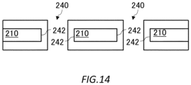
- Fig. 14 is a A-A cross-sectional view.
- the preparation unit 432 may prepare the resin layer 210 having at least one hole 240 penetrating from the upper surface to the lower surface. In the example illustrated in Fig. 13 , the resin layer 210 has four holes 240.
- the generation unit 434 applies molecular bonding agent on the upper surface 211, the lower surface 212 of the resin layer 210 having the hole 240, and the inner face 242 of the hole 240 and performs metal plating to generate the anode collector 200 including the resin layer 210, and the metal layer 231 on the upper surface side of the resin layer 210, the metal layer 232 on the lower surface side of the resin layer 210, and metal arranged on the inner face of the hole 240.
- the metal layer 231 and the metal layer 232 are electrically connected by means of the metal arranged on the inner face of the hole 240. With molecular bonding, such metal plating onto the inner face 242 of the hole 240 can be made achievable.
- the number and size of the hole 240 may be determined according to the type of the resin layer 210, the size of the resin layer 210, the type of the metal, and the like.
- the number and size of appropriate holes 240 may be determined by conducting experiments under various conditions, such as for each type of the resin layer 210, for each size of the resin layer 210, for each type the metal.
- the size of the hole 240 may be 0.01 mm to 5 mm in diameter.
- the spacing between the holes 240 may be 0.05 mm to 5 mm in center-distance.
- the preparation unit 432 may prepare the resin layer 210 having the hole 240 by acquiring the resin layer 210 in which the hole 240 is formed. In addition, the preparation unit 432 may acquire the resin layer 210 in which no hole 240 is formed, to form the hole 240 in the resin layer 210. For example, the preparation unit 432 forms one or more holes 240 on the resin layer 210 by means of chemical etching. By using chemical etching, holes 240 with diameter of 30 ⁇ m to 200 ⁇ m can be formed at a pitch of 100 ⁇ m, for example.
- the preparation unit 432 may form one or more holes 240 on the resin layer 210 by means of ultrasonic laser. In addition, the preparation unit 432 may form one or more holes 240 on the resin layer 210 by means of drilling use a drill for drilling. In addition, the preparation unit 432 may form one or more holes 240 on the resin layer 210 by means of a gas laser.
- the anode collector 200 with reduced weight can be generated, as compared to the anode collector 200 illustrated in Fig. 11 .
- the collector generation unit 430 may generate the anode collector 200 by causing molecular bonding of metal to at least one of the side surfaces 213, the upper surface 211, the lower surface 212 of the resin layer 210, and the inner face 242 of the hole 240. In this manner, conductivity of the anode collector 200 can be enhanced while attempting to reduce the weight of the anode collector 200.
- the generation unit 434 may use sputtering instead of molecular bonding.
- the generation unit 434 form a metal thin film by means of sputtering on the upper surface 211, the lower surface 212, and the inner face 242 of the hole 240 of the resin layer 210 having the hole 240 and performs metal plating to generate the anode collector 200 including the resin layer 210, and the metal layer 231 on the upper surface side of the resin layer 210, the metal layer 232 on the lower surface side of the resin layer 210, and metal arranged on the inner face of the hole 240.
- Fig. 15 schematically illustrate an example of flow of processing performed by a collector generation unit 430.
- flow of processing where a plurality of collectors having an active material is generated is described.
- the preparation unit 432 prepares a quadrangular-shaped resin layer.
- the generation unit 434 causes molecular bonding of metal to the resin layer prepared at S102.
- the generation unit 434 may cause molecular bonding of metal to the entire resin layer.
- the generation unit 434 may cause molecular bonding of metal to at least a part of the side surfaces, the upper surface, and the lower surface of the resin layer.
- the generation unit 434 may use sputtering instead of molecular bonding.
- the generation unit 434 arranges the active material on the metal layer on the upper surface of the resin layer. For example, the generation unit 434 arranges the active material in a region other than the first end of the upper surface of the metal layer.
- the generation unit 434 cuts the resin layer on which the active material is arranged at S106, to generate a plurality of collectors each including both a part of the first end and a portion on which the active material is arranged.
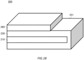
- Fig. 16 to Fig. 18 are illustrations for describing the manufacturing process of the anode collector 200.
- the generation unit 434 generates a quadrangular-shaped resin layer 210 (this may be described as multilayered body 250) on which metal is arranged to its entirety.
- the generation unit 434 may arrange metal by means of molecular bonding, or may arrange metal by means of sputtering.
- Fig. 16 is a top view of the multilayered body 250.
- the multilayered body 250 may have a belt-like shape.
- the generation unit 434 arranges an active material 260 on a region 255 other than the end 253 opposing the end 251 and the end 251 of the upper surface of the multilayered body 250 and cuts the multilayered body 250, thereby generating a plurality of anode collectors 200 each including both a part of the end 251 or a part of the end 253, and a portion on which the active material is arranged. As illustrated in Fig.
- the generation unit 434 may generate the plurality of anode collectors 200 each including both a part of the end 251 or the part of the end 253, and a portion on which the active material is arranged, by arranging the active material 260 on the region 255 and cutting each of the partial resin layer 256 including the end 251 and the partial resin layer 257 including the end 253, that are cut at a portion where the active material 260 is arranged.
- Generation of the multilayered body 250, arrangement of the active material 260 and the like may be achieved by any methods, and roll-to-roll process or the like may be adopted, for example.
- anode collector 200 in which metal is arranged on two side surfaces and ten anode collectors 200 in which metal is arranged on one side surface are manufactured.
- a plurality of anode collectors 200 can be generated efficiently.
- description is made for the manufacturing process of the anode collector 200 in Fig. 16 to Fig. 18 it also applies to the manufacturing process of the cathode collector 300.
- Fig. 19 schematically illustrates an example of flow of processing performed by the collector generation unit 430.
- flow of processing where a plurality of collectors having an active material is generated is described.
- the preparation unit 432 prepares a quadrangular-shaped resin layer.
- the generation unit 434 causes molecular bonding of metal to the resin layer prepared at S202.
- the generation unit 434 may cause molecular bonding of metal to the entire resin layer. Note that, the generation unit 434 may cause molecular bonding of metal to at least a part of the side surfaces, the upper surface, and the lower surface of the resin layer.
- the generation unit 434 may use sputtering instead of molecular bonding.
- the generation unit 434 arranges the active material on the metal layer on the upper surface of the resin layer. For example, the generation unit 434 arranges the active material in a region other than the first end of the upper surface of the metal layer.
- the generation unit 434 cuts a part of the portion of the first end of the resin layer, thereby cutting the first end into a saw shape to form a plurality of convex portions in a portion of the first end.
- the generation unit 434 cuts the resin layer into a rectangular shape, to generate a plurality of collectors each including both one convex portion and a portion on which the active material is arranged.
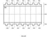
- Fig. 20 and Fig. 21 are illustrations for describing the manufacturing process of the anode collector 200.
- the generation unit 434 arranges the active material 260 on a region 255 other than the end 253 opposing the end 251 and the end 251 on the upper surface of the multilayered body 250, and cuts a part of the portion of the end 251 of the multilayered body 250, thereby forming a plurality of convex portions 252 in a portion of the end 251, cuts a part of the portion of the end 253 of the multilayered body 250, thereby forming a plurality of convex portions 254 in a portion of the end 253, and cuts the multilayered body 250, thereby generating the plurality of anode collectors 200 each including both one convex portion 252 or one convex portion 254, and a portion on which the active material 260 is arranged.
- the anode collector 200 with secured conductivity by means of the metal layer at the tip portion of the convex portion can be generated.
- description is made for the manufacturing process of the anode collector 200 in Fig. 20 and Fig. 21 , it also applies to the manufacturing process of the cathode collector 300.
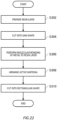
- Fig .22 schematically illustrate an example of flow of processing performed by the collector generation unit 430.
- flow of processing where a plurality of collectors having an active material is generated is described.
- the preparation unit 432 prepares a quadrangular-shaped resin layer.
- the generation unit 434 cuts a part of the portion of the first end of the resin layer, thereby cutting the first end into a saw shape to form a plurality of convex portions in a portion of the first end.
- the generation unit 434 causes molecular bonding of metal to the entire resin layer on which the plurality of convex portions are formed at a portion of the first end at S304.
- the generation unit 434 may use sputtering instead of molecular bonding.
- the generation unit 434 arranges the active material on a region on the upper surface in a portion other than the first end of the resin layer.
- the generation unit 434 generates the plurality of collectors each including both one convex portion and a portion on which the active material is arranged, by cutting the resin layer into a rectangular shape.
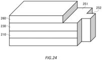
- Fig. 23 and Fig. 24 are illustrations for describing the manufacturing process of the anode collector 200.
- the generation unit 434 forms a plurality of convex portions 222 at the end 221 by cutting a part of the end 221 of the quadrangular-shaped resin layer 210, forms a plurality of convex portions 224 at the end 223 by cutting a part of the end 223 of the resin layer 210, and thereafter causes molecular bonding of metal to the entire resin layer 210, arranges the active material on a region 225 on the upper surface of a portion other than the end 221 and the end 223 of the resin layer 210, and cuts the resin layer 210, thereby generating a plurality of anode collectors 200 each including both one convex portion 222 or one convex portion 224, and a portion on which the active material is arranged.
- the generation unit 434 may cut the resin layer 210 into a rectangular shape. Although description is made for the manufacturing process of the anode collector 200 in Fig. 23 and Fig. 24 , it also applies to the manufacturing process of the cathode collector 300.
- the generation unit 434 may use sputtering instead of molecular bonding.
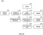
- Fig. 25 schematically illustrates an example of a hardware configuration of a computer 1200 that functions as the manufacturing system 400.
- a program installed in the computer 1200 can cause the computer 1200 to function as one or more "units" of a device according to the present embodiment, or cause the computer 1200 to perform operations associated with the device or perform one or more "units” thereof according to the present embodiment, and/or cause the computer 1200 to perform the process according to the present embodiment or perform the steps of the process.
- Such a program may be executed by a CPU 1212 to cause the computer 1200 to perform particular operations associated with some or all of the blocks in the flowcharts and block diagrams described in the specification.
- the computer 1200 includes the CPU 1212, a RAM 1214, and a graphics controller 1216, which are connected to each other via a host controller 1210.
- the computer 1200 also includes input/output units such as a communication interface 1222, a storage device 1224, a DVD drive and an IC card drive, which are connected to the host controller 1210 via an input/output controller 1220.
- the DVD drive may be a DVD-ROM drive, a DVD-RAM drive, and the like.
- the storage device 1224 may be a hard disk drive, a solid-state drive, and the like.
- the computer 1200 also includes a ROM 1230 and a legacy input/output unit such as a keyboard, which are connected to the input/output controller 1220 via an input/output chip 1240.
- the CPU 1212 operates according to the programs stored in the ROM 1230 and the RAM 1214, thereby controlling each unit.
- the graphics controller 1216 obtains image data which is generated by the CPU 1212 in a frame buffer or the like provided in the RAM 1214 or in itself so as to cause the image data to be displayed on a display device 1218.
- the communication interface 1222 communicates with other electronic devices via a network.
- the storage device 1224 stores a program and data used by the CPU 1212 in the computer 1200.
- the DVD drive reads the programs or the data from the DVD-ROM or the like, and provides the storage device 1224 with the programs or the data.
- the IC card drive reads programs and data from an IC card and/or writes programs and data into the IC card.
- the ROM 1230 stores therein a boot program or the like executed by the computer 1200 at the time of activation, and/or a program depending on the hardware of the computer 1200.
- the input/output chip 1240 may also connect various input/output units via a USB port, a parallel port, a serial port, a keyboard port, a mouse port, or the like to the input/output controller 1220.
- a program is provided by a computer readable storage medium such as the DVD-ROM or the IC card.
- the program is read from the computer readable storage medium, installed into the storage device 1224, RAM 1214, or ROM 1230, which are also examples of a computer readable storage medium, and executed by the CPU 1212.
- Information processing written in these programs is read by the computer 1200, and provides cooperation between the programs and the various types of hardware resources described above.
- a device or method may be constituted by realizing the operation or processing of information in accordance with the usage of the computer 1200.
- the CPU 1212 may execute a communication program loaded in the RAM 1214 and instruct the communication interface 1222 to perform communication processing based on a process written in the communication program.
- the communication interface 1222 under control of the CPU 1212, reads transmission data stored on a transmission buffer region provided in a recording medium such as the RAM 1214, the storage device 1224, the DVD-ROM, or the IC card, and transmits the read transmission data to a network or writes reception data received from a network to a reception buffer region or the like provided on the recording medium.
- the CPU 1212 may cause all or a necessary portion of a file or a database to be read into the RAM 1214, the file or the database having been stored in an external recording medium such as the storage device 1224, the DVD drive (DVD-ROM), the IC card, etc., and perform various types of processing on the data on the RAM 1214. Then, the CPU 1212 may write the processed data back in the external recording medium.
- an external recording medium such as the storage device 1224, the DVD drive (DVD-ROM), the IC card, etc.
- the CPU 1212 may execute, on the data read from the RAM 1214, various types of processing including various types of operations, information processing, conditional judgement, conditional branching, unconditional branching, information retrieval/replacement, or the like described throughout the present disclosure and specified by instruction sequences of the programs, to write the results back to the RAM 1214.
- the CPU 1212 may retrieve information in a file, a database, or the like in the recording medium.
- the CPU 1212 may search for an entry whose attribute value of the first attribute matches a designated condition, from among the plurality of entries, and read the attribute value of the second attribute stored in the entry, thereby obtaining the attribute value of the second attribute associated with the first attribute satisfying a predetermined condition.
- the above described program or software modules may be stored in the computer readable storage medium on or near the computer 1200.
- a recording medium such as a hard disk or a RAM provided in a server system connected to a dedicated communication network or the Internet can be used as the computer readable storage medium, thereby providing the program to the computer 1200 via the network.
- Blocks in flowcharts and block diagrams in the present embodiments may represent steps of processes in which operations are performed or "units" of devices responsible for performing operations.
- a specific step and "unit” may be implemented by dedicated circuitry, programmable circuitry supplied along with a computer readable instruction stored on a computer readable storage medium, and/or a processor supplied along with the computer readable instruction stored on the computer readable storage medium.
- the dedicated circuitry may include a digital and/or analog hardware circuit, or may include an integrated circuit (IC) and/or a discrete circuit.
- the programmable circuitry may include, for example, a reconfigurable hardware circuit including logical AND, logical OR, logical XOR, logical NAND, logical NOR, and other logical operations, and a flip-flop, a register, and a memory element, such as a field-programmable gate array (FPGA) and a programmable logic array (PLA).
- a reconfigurable hardware circuit including logical AND, logical OR, logical XOR, logical NAND, logical NOR, and other logical operations, and a flip-flop, a register, and a memory element, such as a field-programmable gate array (FPGA) and a programmable logic array (PLA).
- FPGA field-programmable gate array
- PLA programmable logic array
- the computer readable storage medium may include any tangible device capable of storing an instruction performed by an appropriate device, so that the computer readable storage medium having the instruction stored thereon constitutes a product including an instruction that may be performed in order to provide means for performing an operation specified by a flowchart or a block diagram.
- Examples of the computer readable storage medium may include an electronic storage medium, a magnetic storage medium, an optical storage medium, an electromagnetic storage medium, a semiconductor storage medium, and the like.
- the computer readable storage medium may include a floppy (registered trademark) disk, a diskette, a hard disk, a random access memory (RAM), a read only memory (ROM), an erasable programmable read only memory (EPROM or flash memory), an electrically erasable programmable read only memory (EEPROM), a static random access memory (SRAM), a compact disk read only memory (CD-ROM), a digital versatile disk (DVD), a Blu-ray (registered trademark) disk, a memory stick, an integrated circuit card, or the like.
- a floppy (registered trademark) disk a diskette, a hard disk, a random access memory (RAM), a read only memory (ROM), an erasable programmable read only memory (EPROM or flash memory), an electrically erasable programmable read only memory (EEPROM), a static random access memory (SRAM), a compact disk read only memory (CD-ROM), a digital versatile disk (DVD), a Blu-ray (registere
- the computer readable instruction may include an assembler instruction, an instruction-set-architecture (ISA) instruction, a machine instruction, a machine dependent instruction, a microcode, a firmware instruction, state-setting data, or either of source code or object code written in any combination of one or more programming languages including an object-oriented programming language such as Smalltalk (registered trademark), JAVA (registered trademark), and C++, and a conventional procedural programming language such as a "C" programming language or a similar programming language.
- ISA instruction-set-architecture
- machine instruction e.g., JAVA (registered trademark), and C++
- a conventional procedural programming language such as a "C" programming language or a similar programming language.
- the computer readable instruction may be provided to a general purpose computer, a special purpose computer, or a processor or programmable circuitry of another programmable data processing apparatus locally or via a local area network (LAN), a wide area network (WAN) such as the Internet or the like in order that the general purpose computer, the special purpose computer, or the processor or the programmable circuitry of the other programmable data processing apparatus performs the computer readable instruction to provide means for performing operations specified by the flowchart or the block diagram.
- An example of the processor includes a computer processor, processing unit, microprocessor, digital signal processor, controller, microcontroller, or the like.
Landscapes
- Chemical & Material Sciences (AREA)
- Chemical Kinetics & Catalysis (AREA)
- Electrochemistry (AREA)
- General Chemical & Material Sciences (AREA)
- Engineering & Computer Science (AREA)
- Materials Engineering (AREA)
- Composite Materials (AREA)
- Cell Electrode Carriers And Collectors (AREA)
- Connection Of Batteries Or Terminals (AREA)
- Sealing Battery Cases Or Jackets (AREA)
Abstract
Description
- The present invention relates to a manufacturing method, a program, a manufacturing system, a multilayer collector, a battery, a moving body, and a flight vehicle.
- Metal plated resin film has been known (see
Patent document 1, for example). - Patent Document 1:
Japanese Patent Application Publication No. 2018-181823 - According to an embodiment of the present invention, a manufacturing method of a multilayer collector is provided. The manufacturing method may comprise preparing a resin layer, and a laminate in which collectors including a first metal layer and a second metal layer arranged on both sides of the resin layer are laminated. The manufacturing method may comprise arranging a tab on one of an upper surface side and a lower surface side of the laminate, and a Sub-tab on another. The manufacturing method may comprise performing heat compression on a portion to be welded of the tab, the laminate, and the Sub-tab in a laminating direction, to elute resin of the resin layer in the portion to be welded. The manufacturing method may comprise performing resistance welding on the portion to be welded.
- A manufacturing method of a multilayer collector according to
claim 1, wherein in the performing heat compression, only the portion to be welded of the tab, the laminate, and the Sub-tab are subjected to heat compression in a laminating direction, to elute resin in the resin layer of the portion to be welded. In the preparing, the laminate may be prepared in which the collectors including the resin layer, the first metal layer, and the second metal layer, which has a thickness that satisfies a followingnumerical expression 1, are laminated.
- In the preparing, the laminate may be prepared in which the collectors including a resin layer with a thickness of 3 to 7 µm, the first metal layer with a thickness of 0.1 to 2 µm, and the second metal layer with a thickness of 0.1 to 2 pm are laminated. The portion to be welded may have a circular shape with a diameter of 1 to 10 mm. A diameter of the portion to be welded, a total of a thickness of the first metal layer and a thickness of the second metal layer, and a thickness of the resin layer may satisfy a following numerical expression 2.

- A diameter of the portion to be welded, a total of a thickness of the first metal layer and a thickness of the second metal layer, and a thickness of the resin layer may satisfy a following numerical expression 3.

- A diameter of the portion to be welded, a total of a thickness of the first metal layer and a thickness of the second metal layer, and a thickness of the resin layer may satisfy a following numerical expression 4.

- A diameter of the portion to be welded, a total of a thickness of the first metal layer and a thickness of the second metal layer, and a thickness of the resin layer may satisfy a following numerical expression 5.

- Thermal contraction in TD direction of resin in the resin layer may be 1% or less. Material of the first metal layer and the second metal layer may be copper, and material of the resin layer may be polyimide, polypropylene, polyethylene, polyphenylene sulfide, or polyethylene terephthalate. A thickness of the tab may be 100 to 300 µm. The thickness of the tab may be determined within the range of 100 to 300 µm depending on the size of the current value. For example, the thickness of the Sub-tab may be 50 to 100 µm. The portion to be welded may have a polygonal shape.
- According to an embodiment of the present invention, a program for causing a computer to perform the manufacturing method of a multilayer collector is provided.
- According to an embodiment of the present invention, a manufacturing method of a battery is provided. The manufacturing method may comprise preparing a resin layer having a thickness of 3 to 7 µm and a laminate in which collectors including a first metal layer and a second metal layer each having a thickness of 0.1 to 2 µm arranged on both sides of the resin layer are laminated. The manufacturing method may comprise arranging a tab on one of an upper surface side and a lower surface side of the laminate, and a Sub-tab on another. The manufacturing method may comprise performing heat compression on a portion to be welded with a diameter of 1 to 10 mm of the tab, the laminate, and the Sub-tab in a laminating direction, to elute resin in the resin layer of the portion to be welded. The manufacturing method may comprise performing resistance welding on the portion to be welded to generate a multilayer collector. The manufacturing method may comprise generating a battery of a flight vehicle having a solar panel and the battery mounted thereon that utilizes electrical power of the battery by using the multilayer collector. In the generating the battery, the battery of a HAPS having the solar panel and the battery mounted thereon that flies in a stratosphere to provide wireless communication service on ground may be generated by using the multilayer collector.
- According to an embodiment of the present invention, a manufacturing system is provided. The manufacturing system may comprise a preparation unit that prepares a resin layer, and a laminate in which collectors including a first metal layer and a second metal layer arranged on both sides of the resin layer are laminated. The manufacturing system may comprise an arrangement unit that arranges a tab on one of an upper surface side and a lower surface side of the laminate, and a Sub-tab on another. The manufacturing system may comprise a heat compression unit that performs heat compression on a portion to be welded of the tab, the laminate, and the Sub-tab in a laminating direction, to elute resin of the resin layer in the portion to be welded. The manufacturing system may comprise a welding unit that performs resistance welding on the portion to be welded.
- According to an embodiment of the present invention, a multilayer collector in which a plurality of collectors are laminated with a tab arranged on one of an upper side and a lower side and a Sub-tab on another is provided. The multilayer collector may comprise a first region that is not between the tab and the Sub-tab, including a resin layer intermediate between each of the plurality of collectors, a second region that is between the tab and the Sub-tab, including a resin layer intermediate between each of the plurality of collectors, and a third region that is between the tab and the Sub-tab, having less amount of resin intermediate between each of the plurality of collectors than an amount of resin in each resin layer between the plurality of collectors in the first region or having no resin intermediate between each of plurality of the collectors, the third region being subjected to resistance welding.
- According to an embodiment of the present invention, a battery having the multilayer collector is provided. According to an embodiment of the invention, a moving body having the battery is provided. According to an embodiment of the invention, a flight vehicle having the battery is provided.
- According to an embodiment of the present invention, a manufacturing method of a collector is provided. The manufacturing method may comprise preparing a resin layer. The manufacturing method may comprise generating a collector in which metal is arranged on at least a part of side surfaces, an upper surface, and a lower surface of the resin layer, and the metal layer on the upper surface and the metal layer on the lower surface are electrically connected by means of metal on at least a part of the side surfaces.
- In the generating, the metal may be arranged by performing molecular bonding of the metal to at least a part of side surfaces, an upper surface, and a lower surface of the resin layer. In the generating, metal may be arranged on at least a part of side surfaces, an upper surface, and a lower surface of the resin layer by means of sputtering. In the generating, metal thin film may be formed on at least a part of side surfaces, an upper surface, and a lower surface of the resin layer by means of sputtering, and the metal may be plated onto the metal thin film. In the generating, the metal may be arranged on at least one side surface of four side surfaces, an upper surface, and a lower surface of the quadrangular-shaped resin layer to generate the collector. In the generating, a plurality of the collectors in which the metal is arranged on at least one side surface may be generated by arranging the metal on the entire resin layer and cutting it. In the preparing, the resin layer having at least one hole penetrating from the upper surface to the lower surface may be prepared, and in the generating, the metal may be arranged on at least a part of side surfaces, an upper surface, and a lower surface of the resin layer, and an inner face of the hole, to generate the collector.
- In the generating, by arranging an active material in a region other than a first end of an upper surface of a layer of the metal in the quadrangular-shaped resin layer with the metal arranged on its entirety and cutting it, a plurality of the collector each including both a part of the first end and a portion in which the active material is arranged may be generated. In the generating, by arranging an active material in a region other than a first end of an upper surface of a layer of the metal in the quadrangular-shaped resin layer with the metal arranged on its entirety, and cutting a part of the portion of the first end of the resin layer, a plurality of convex portions are formed at the portion of the first end, and by cutting the resin layer, a plurality of the collector each including both one of the plurality of convex portions and a portion in which the active material is arranged may be generated.
- In the generating, by arranging an active material in a region other than a first end and a second end opposing the first end of an upper surface of a layer of the metal in the quadrangular-shaped resin layer with the metal arranged on its entirety and cutting it, a plurality of the collector each including both a part of the first end or a part of the second end, and a portion in which the active material is arranged may be generated. In the generating, by arranging an active material in a region other than the first end and the second end of an upper surface of a layer of the metal in the resin layer, and cutting each of a first partial resin layer including the first end and a second partial resin layer including the second end, that are cut at a portion where the active material is arranged, a plurality of the collectors each including both a part of the first end and a portion in which the active material is arranged, and the collectors each including both a part of the second portion and a portion in which the active material is arranged may be generated. In the generating, the active material is arranged in a region other than the first end and the second end on the upper surface of a layer of the metal in the resin layer, and a part of the portion of the first end of the resin layer is cut, thereby forming a plurality of convex portions in a portion of the first end, a part of the portion of the second end of the resin layer is cut, thereby forming a plurality of convex portions in a portion of the second end, and the resin layer is cut, thereby a plurality of the collectors each including both one of the plurality of convex portions in the first end or one of the plurality of convex portions in the second end, and a portion on which the active material is arranged may be generated.
- In the generating, after a plurality of convex portions is formed at the first end by cutting a part of the first end of the quadrangular-shaped resin layer, by arranging the metal on the entire resin layer, arranging the active material in a region on an upper surface of a portion other than the first end of the resin layer, and cutting the resin layer, a plurality of the collectors each including both one of the plurality of convex portions and a portion on which the active material is arranged may be generated. In the generating, after forming a plurality of convex portions at the first end by cutting a part of a portion of the first end of the quadrangular-shaped resin layer and forming a plurality of convex portions at the second end by cutting a part of a portion of the second end opposing the first end of the resin layer, by arranging the metal on the entire resin layer, arranging an active material in a region on the upper surface of a portion other than the first end and the second end of the resin layer and cutting the resin layer, a plurality of the collectors each including both one of the plurality of convex portions in the first end or one of the plurality of convex portions in the second end and a portion on which the active material is arranged may be generated.
- According to an embodiment of the present invention, a manufacturing method is provided. The manufacturing method may comprise preparing a resin layer having at least one hole penetrating from an upper surface to a lower surface. The manufacturing method may comprise generating a collector in which metal is arranged on an upper surface and a lower surface of the resin layer, and an inner face of a hole, and the metal layer on the upper surface and the metal layer on the lower surface are electrically connected by means of metal on the inner face. The collector may be an anode collector having the resin layer and a copper layer arranged in the resin layer. The collector may be a cathode collector having the resin layer and an aluminum layer arranged in the resin layer.
- According to an embodiment of the present invention, a program for causing a computer to perform the above-described manufacturing method of the collector is provided.
- According to an embodiment of the present invention, a manufacturing system is provided. The manufacturing system may comprise a preparation unit that prepares a resin layer. The manufacturing system may comprise a generation unit that generates a collector having metal arranged on at least a part of side surfaces, a upper surface, and a lower surface of a resin layer, and including an intermediate resin layer.
- According to an embodiment of the present invention, a manufacturing system is provided. The manufacturing system may comprise a preparation unit that prepares a resin layer having at least one hole penetrating from an upper surface to a lower surface. The manufacturing system may comprise a generation unit that generate a collector in which metal is arranged on an upper surface and a lower surface of the resin layer, and an inner face of a hole, and the metal layer on the upper surface and the metal layer on the lower surface are electrically connected by means of metal on the inner face.
- According to an embodiment of the present invention, a collector is provided. The collector may include a resin layer, and metal layers arranged on at least a part of side surfaces, an upper surface, and a lower surface of the resin layer, wherein the metal layer on the upper surface and the metal layer on the lower surface may be electrically connected by means of metal in at least a part of the side surface.
- According to an embodiment of the present invention, a collector is provided. The collector may include a resin layer having at least one hole penetrating from an upper surface to a lower surface, and metal arranged on an upper surface and a lower surface of the resin layer, and an inner face of the hole, wherein the metal layer on the upper surface and the metal layer on the lower surface may be electrically connected by means of metal on the inner face.
- According to an embodiment of the present invention, a battery having the collector is provided.
- The summary clause does not necessarily describe all necessary features of the embodiments of the present invention. The present invention may also be a sub-combination of the features described above.
-
-
Fig. 1 schematically illustrates an example of abattery component 10. -
Fig. 2 schematically illustrates another example of thebattery component 10. -
Fig. 3 schematically illustrates an example of a configuration of ananode collector 200. -
Fig. 4 schematically illustrates an example of a configuration of acathode collector 300. -
Fig. 5 schematically illustrates an example of a functional configuration of amanufacturing system 400. -
Fig. 6 is an illustration for describing a manufacturing method of amultilayer collector 100. -
Fig. 7 is an illustration for describing the manufacturing method of themultilayer collector 100. -
Fig. 8 is an illustration for describing the manufacturing method of themultilayer collector 100. -
Fig. 9 is an illustration for describing the manufacturing method of themultilayer collector 100. -
Fig. 10 is an illustration for describing the manufacturing method of themultilayer collector 100. -
Fig. 11 is an illustration for describing plating of aresin layer 210. -
Fig. 12 is an illustration for describing plating of aresin layer 210. -
Fig. 13 is an illustration for describing plating of aresin layer 210. -
Fig. 14 is a A-A sectional view. -
Fig. 15 schematically illustrates an example of flow of processing performed by acollector generation unit 430. -
Fig. 16 is an illustration for describing a manufacturing process of theanode collector 200. -
Fig. 17 is an illustration for describing a manufacturing process of theanode collector 200. -
Fig. 18 is an illustration for describing a manufacturing process of theanode collector 200. -
Fig. 19 schematically illustrates an example of flow of processing performed by thecollector generation unit 430. -
Fig. 20 is an illustration for describing a manufacturing process of theanode collector 200. -
Fig. 21 is an illustration for describing a manufacturing process of theanode collector 200. -
Fig .22 schematically illustrate an example of flow of processing performed by thecollector generation unit 430. -
Fig. 23 is an illustration for describing a manufacturing process of theanode collector 200. -
Fig. 24 is an illustration for describing a manufacturing process of theanode collector 200. -
Fig. 25 schematically illustrates an example of a hardware configuration of acomputer 1200 that functions as themanufacturing system 400. - Hereinafter, the present invention will be described through embodiments of the invention, but the following embodiments do not limit the invention according to claims. In addition, not all of the combinations of features described in the embodiments are essential to the solving means of the invention.
-
Fig. 1 schematically illustrates an example of abattery component 10. Thebattery component 10 has a plurality of anodes 20 andcathodes 30 that are alternately laminated with aseparator 40 in between, as illustrated inFig. 1 . The anode 20 has ananode collector 200. Thecathode 30 has acathode collector 300. - The
battery component 10 may be a component of the battery of any type. Thebattery component 10 is a component of a lithium-ion battery, for example. For example, tabs are welded to each of a laminate 280 in which theanode collectors 200 are laminated and a laminate 380 in which thecathode collectors 300 are laminated, theentire battery component 10 is put into a housing or the like, which is filled with electrolyte, to form a lithium-ion battery. Thebattery component 10 may be a component of a lithium-air battery. Thebattery component 10 may be a component of a battery of another type. - In
Fig. 1 , although a case where theanode collector 200 and thecathode collector 300 are arranged in the same direction is illustrated, it is not limited thereto. Theanode collector 200 and thecathode collector 300 may be arranged in different directions. For example, theanode collector 200 and thecathode collector 300 may be arranged in opposite directions. -
Fig. 2 schematically illustrates another example of thebattery component 10. Thebattery component 10 has alaminate battery 50 that is laminated, as illustrated inFig. 2 . Thelaminate battery 50 has theanode collector 200 and thecathode collector 300. For example, when thebattery component 10 is a component of a lithium-ion battery, a tab is welded to each of the laminate 280 and the laminate 380, and theentire battery component 10 is put into a housing or the like, thereby forming a lithium-ion battery. - In
Fig. 2 , a case where theanode collector 200 and thecathode collector 300 are arranged in the same direction is illustrated, but it is not limited thereto. Theanode collector 200 and thecathode collector 300 may be arranged in different directions. For example, theanode collector 200 and thecathode collector 300 may be arranged in opposite directions. -
Fig. 3 schematically illustrates an example of a configuration of theanode collector 200. Theanode collector 200 illustrated inFig. 3 has aresin layer 210, and ametal layer 231 and ametal layer 232 arranged on both sides of theresin layer 210. Theanode collector 200 has, for example, theresin layer 210, and themetal layer 231 and themetal layer 231 coated on theresin layer 210. - As resin in the
resin layer 210 according to the present embodiment, resin having lower conductivity than the metal of themetal layer 231 and themetal layer 232 but having a lower density than the metal of themetal layer 231 and themetal layer 232 is adopted. An example of resin in theresin layer 210 includes PI (polyimide). In addition, an example of the resin in theresin layer 210 includes PET (polyethylene terephthalate). PP (polypropylene), PE (polyethylene), PPS (polyphenylene sulfide) and the like may be used as resin in theresin layer 210. These are illustrative, and other types of resin may be used as resin in theresin layer 210. For example, when thebattery component 10 is a component of a lithium-ion battery, the metal of themetal layer 231 and themetal layer 232 may be copper, and the resin in theresin layer 210 may be polyimide. The metal of themetal layer 231 and themetal layer 232 may be other metal. - Depending on the application of the battery, there may be cases where the current may be low but it is desired to reduce the weight. For example, for a flight vehicle with a solar panel and a battery mounted thereon that utilizes electrical power of the battery, since there is less change in flight speed, the output current of the battery may be low, but the weight of the entire flight vehicle is required to be light. Examples of such a flight vehicle include HAPS (High Altitude Platform Station) that flies in the stratosphere to provide wireless communication service on the ground, airplanes, and the like. There are other applications in which the current may be low but it is requested to reduce the weight, in this manner.
- For example, for a lithium-ion battery, copper foil is often used as the anode collector, and such a request can be met by reducing the thickness of the copper foil. However, there is a technical limitation in reducing the thickness of the copper foil, and also, if the thickness of the copper foil is reduced too much, the strength cannot be maintained and the possibility of breakage increases. Since the intermediate part of the
anode collector 200 according to the present embodiment is aresin layer 210, electric resistance is increased but the density can be reduced as compared to an anode collector formed solely of metal. In addition, the strength of theanode collector 200 can be maintained. - For example, when the metal of the
metal layer 230 is copper, and supposing that the resin in theresin layer 210 is PET, since the density of copper is about 8.96 g/cm3 and the density of PET is about 1.38 g/cm3, the weight can be significantly reduced compared to a case where the anode collector is composed solely of copper. - For example, when it is assumed that the thickness of the
anode collector 200 is 8 µm, supposing that the thickness of theresin layer 210 is 6 µm, the density is about 3.25 g/cm3, which results in a weight ratio of approximately 35% compared to a case where it is composed solely of copper, allowing reduction of approximately 65% in weight. In addition, supposing that the thickness of theresin layer 210 is 7 µm, the density is about 2.30 g/cm3, which results in a weight ratio of approximately 25% compared to a case where it is composed solely of copper, allowing reduction of approximately 75% in weight. - In a case where the anode collector is composed solely of metal, even if the anode collector is multi-layered, a conduction path can be secured between metal (between conductive materials) by welding such as ultrasonic welding, resistance welding, and laser welding. By contrast, when the anode collector having an intermediate resin layer is multi-layered, a conduction path cannot be secured. Thus, it cannot be subjected to resistance welding as it is. In addition, since features such as boiling point, thermal expansion, strength and the like may differ between the metal layer and the resin layer, when laser welding is attempted, problems such as disruption or remaining of vacant holes may occur. In addition, when ultrasonic welding is attempted, crack or breaking may occur.
-
Fig. 4 schematically illustrates an example of a configuration of acathode collector 300. Thecathode collector 300 according to the present embodiment has a resin layer 310, and a metal layer 331 and ametal layer 332 arranged on both sides of the resin layer 310. Thecathode collector 300 has, for example, the resin layer 310, and the metal layer 331 and themetal layer 332 coated on the resin layer 310. - As resin in the resin layer 310 according to the present embodiment, resin having lower conductivity than the metal of the metal layer 331 and the
metal layer 332 but having a lower density than the metal of the metal layer 331 and themetal layer 332 is adopted. An example of resin in the resin layer 310 includes PI (polyimide). In addition, an example of the resin in the resin layer 310 includes PET (polyethylene terephthalate). PP (polypropylene), PE (polyethylene), PPS (polyphenylene sulfide) and the like may be used as resin in the resin layer 310. These are illustrative, and other types of resin may be used as resin in the resin layer 310. For example, when thebattery component 10 is a component of a lithium-ion battery, the metal of the metal layer 330 may be aluminum, and the resin in the resin layer 310 may be polyimide. The metal of the metal layer 330 may be other metal. -
Fig, 5 schematically illustrates an example of a functional configuration of amanufacturing system 400. Themanufacturing system 400 comprises apreparation unit 402, a multilayercollector generation unit 410, abattery generation unit 420, and acollector generation unit 430. Note that, it is no necessarily imperative that themanufacturing system 400 comprises all of the above. - The
manufacturing system 400 may be configured by one device. In addition, themanufacturing system 400 may be configured by a plurality of devices. For example, themanufacturing system 400 is configured by a device comprising thepreparation unit 402 and thebattery generation unit 420, a device comprising thebattery generation unit 420, and a device comprising thecollector generation unit 430. Themanufacturing system 400 may not comprise thebattery generation unit 420. Themanufacturing system 400 may not comprise thecollector generation unit 430. - The
preparation unit 402 prepares the laminate 280 and thelaminate 380. Thepreparation unit 402 may prepare thebattery component 10. Thepreparation unit 402 prepares thebattery component 10 by receiving thebattery component 10 from another device, for example. Thepreparation unit 402 may prepare thebattery component 10 by laminating an anode 20, acathode 30, and aseparator 40. Thelaminate preparation unit 402 may prepare thebattery component 10 by laminating alaminate battery 50. - The thickness of the
resin layer 210 may be 3 to 7 µm. Examples of the thickness of theresin layer 210 include 3 µm, 4 µm, 5 µm, 6 µm, 7 pm and the like. - The thickness of the
metal layer 231 may be 0.1 to 2 µm. The thickness of themetal layer 231 may be, for example, 0.5 µm to 1 µm. Examples of the thickness of themetal layer 231 include 0.1 µm, 0.2 µm, 0.3 µm, 0.4 µm, 0.5 µm, 0.6 µm, 0.7 µm, 0.8 µm, 09 µm, 1 µm, 1.1 µm, 1.2 µm, 1.3 µm, 1.4 µm, 1.5 µm, 1.6 µm, 1.7 µm, 1.8 µm, 1.9 µm, 2 µm and the like. - The thickness of the
metal layer 232 may be 0.1 to 2 µm. The thickness of themetal layer 232 may be, for example, 0.5 µm to 1 µm. Examples of the thickness of themetal layer 232 include 0.1 µm, 0.2 µm, 0.3 µm, 0.4 µm, 0.5 µm, 0.6 µm, 0.7 µm, 0.8 µm, 09 µm, 1 µm, 1.1 µm, 1.2 µm, 1.3 µm, 1.4 µm, 1.5 µm, 1.6 µm, 1.7 µm, 1.8 µm, 1.9 µm, 2 µm and the like. - Thermal contraction in TD (transverse direction) direction of the resin in the
resin layer 210 may be 1% or less. Thepreparation unit 402 may prepare thebattery component 10 in which theresin layer 210 is composed of resin with thermal contraction in the TD direction of 1% or less. Thepreparation unit 402 may prepare thebattery component 10 in which theresin layer 210 is composed of resin with thermal contraction in the TD direction of 1% or less, by adjusting the material, the manufacturing method, the machining method and the like. - Thermal contraction in the TD direction of the resin in the resin layer 310 may be 1% or less. The
preparation unit 402 may prepare thebattery component 10 in which the resin layer 310 is composed of resin with thermal contraction in the TD direction of 1% or less. Thepreparation unit 402 may prepare thebattery component 10 in which the resin layer 310 is composed of resin with thermal contraction in the TD direction of 1% or less, by adjusting the material, the manufacturing method, the machining method and the like. - The
preparation unit 402 may prepare the laminate 280 in which theanode collectors 200 including theresin layer 210, themetal layer 231, and themetal layer 232 are laminated, having a thickness that satisfies the following numerical expression 6.
- The thickness of the resin layer 310 may be 3 to 7 µm. Examples of the thickness of the resin layer 310 include 3 µm, 4 µm, 5 µm, 6 µm, 7 µm and the like.
- The thickness of the metal layer 331 may be 0.1 to 2 µm. The thickness of the metal layer 331 may be, for example, 0.5 µm to 1 µm. Examples of the thickness of the metal layer 331 include 0.1 µm, 0.2 µm, 0.3 µm, 0.4 µm, 0.5 µm, 0.6 µm, 0.7 µm, 0.8 µm, 09 µm, 1 µm, 1.1 µm, 1.2 µm, 1.3 µm, 1.4 µm, 1.5 µm, 1.6 µm, 1.7 µm, 1.8 µm, 1.9 µm, 2 µm and the like.
- The thickness of the
metal layer 332 may be 0.1 to 2 µm. The thickness of themetal layer 332 may be, for example, 0.5 µm to 1 µm. Examples of the thickness of themetal layer 332 include 0.1 µm, 0.2 µm, 0.3 µm, 0.4 µm, 0.5 µm, 0.6 µm, 0.7 µm, 0.8 µm, 09 µm, 1 µm, 1.1 µm, 1.2 µm, 1.3 µm, 1.4 µm, 1.5 µm, 1.6 µm, 1.7 µm, 1.8 µm, 1.9 µm, 2 µm and the like. - The
preparation unit 402 may prepare the laminate 380 in which thecathode collectors 300 including the resin layer 310, the metal layer 331, and themetal layer 332 are laminated, having a thickness that satisfies the numerical expression in which the thickness of themetal layer 231, the thickness of themetal layer 232, and the thickness of theresin layer 210 in the above-described numerical expression 6 is substituted with the thickness of the metal layer 331, the thickness of themetal layer 332, and the thickness of the resin layer 310. - The multilayer
collector generation unit 410 generates the multilayer collector from the laminate 280 and the laminate 380 prepared by thepreparation unit 402. The multilayercollector generation unit 410 comprises anarrangement unit 412, aheat compression unit 414, and awelding unit 416. - The
arrangement unit 412 arranges a tab on one of the upper surface side and the lower surface side of the laminate 280 and a Sub-tab on another, for example. Thearrangement unit 412 arranges the tab on the upper surface side of the laminate 280, and arranges the Sub-tab on the lower surface side of the laminate 280, for example. Thearrangement unit 412 arranges the Sub-tab on the upper surface side of the laminate 280, and arranges the tab on the lower surface side of the laminate 280, for example. - The
arrangement unit 412 arranges a tab on one of the upper surface side and the lower surface side of the laminate 380, and a Sub-tab on another, for example. Thearrangement unit 412 arranges the tab on the upper surface side of the laminate 380, and arranges the Sub-tab on the lower surface side of the laminate 380, for example. Thearrangement unit 412 arranges the Sub-tab on the upper surface side of the laminate 380, and arranges the tab on the lower surface side of the laminate 380, for example. - The material of the tab to be arranged on the laminate 280 may be the same as the material of the
metal layer 231 and themetal layer 232. For example, when the material of themetal layer 231 and themetal layer 232 is copper, the material of the tab to be arranged on the laminate 280 may also be copper. Note that, the material of the tab to be arranged on the laminate 280 may be different from the material of themetal layer 231 and themetal layer 232. - The material of the tab to be arranged on the laminate 380 may be the same as the material of the metal layer 331 and the
metal layer 332. For example, when the material of the metal layer 331 and themetal layer 332 is aluminum, the material of the tab to be arranged on the laminate 380 may also be aluminum. Note that, the material of the tab to be arranged on the laminate 380 may be different from the material of the metal layer 331 and themetal layer 332. - The thickness of the tab is desirably 100 to 300 µm. The thickness of the tab may be determined within the range of 100 to 300 µm depending on the size of the current value.
- The thickness of the Sub-tab is better to be thick from the perspective of maintaining the strength of the multilayer collector, but better to be thin from the perspective of reducing the weight of the multilayer collector. For example, the thickness of the Sub-tab is desirably 50 to 100 µm.
- The
heat compression unit 414 performs heat compression on the portion to be welded of the tab, the laminate 280, and the Sub-tab in the laminating direction to elute the resin in theresin layer 210 of the portion to be welded. Theheat compression unit 414 may perform heat compression on only the portion to be welded of the tab, the laminate 280, and the Sub-tab in the laminating direction to elute the resin in theresin layer 210 of the portion to be welded. Theheat compression unit 414 may perform heat compression at a temperature according to the type of the resin in theresin layer 210. The temperature according to the type of the resin is a temperature corresponding to the melting point of the resin or higher, for example, which is a predetermined temperature. - The
heat compression unit 414 performs heat compression on the portion to be welded of the tab, the laminate 380, and the Sub-tab in the laminating direction to elute the resin in the resin layer 310 of the portion to be welded. Theheat compression unit 414 may perform heat compression on only the portion to be welded of the tab, the laminate 380, and the Sub-tab in the laminating direction to elute the resin in the resin layer 310 of the portion to be welded. Theheat compression unit 414 may perform heat compression at a temperature according to the type of the resin in the resin layer 310. The temperature according to the type of the resin is a temperature corresponding to the melting point of the resin or higher, for example, which is a predetermined temperature. - The
welding unit 416 performs resistance welding on the portion to be welded of the tab, the laminate 280, and the Sub-tab, having been subjected to heat compression by theheat compression unit 414. Themultilayer collector 100 is generated by thewelding unit 416 performing resistance welding on said portion to be welded. Thewelding unit 416 performs resistance welding on the portion to be welded of the tab, the laminate 380, and the Sub-tab, having been subjected to heat compression by theheat compression unit 414. The multilayer collector 150 is generated by thewelding unit 416 performing resistance welding on said portion to be welded. As a device for performing resistance welding, precision resistance welding machine from NAG System or the like may be adopted, for example. - The portion to be welded has a circular shape having a diameter of 1 to 10 mm, for example. The portion to be welded desirably has a circular shape of 3 to 5 mm. Note that, the shape of the portion to be welded is not limited to a circular shape, and may be a polygonal shape. The diameter of the portion to be welded, the total of the thickness of the
metal layer 231 and the thickness of themetal layer 232, and the thickness of theresin layer 210 may be determined to satisfy the following numerical expression 7. Themanufacturing system 400 may be designed such that the diameter of the portion to be welded, the total of the thickness of themetal layer 231 and the thickness of themetal layer 232, and the thickness ofresin layer 210 satisfy the following numerical expression 7.
- The diameter of the portion to be welded, the total of the thickness of the
metal layer 231 and the thickness of themetal layer 232, and the thickness of theresin layer 210 may be determined to satisfy the following numerical expression 8. Themanufacturing system 400 may be designed such that the diameter of the portion to be welded, the total of the thickness of themetal layer 231 and the thickness of themetal layer 232, and the thickness ofresin layer 210 satisfy the following numerical expression 8.
- The diameter of the portion to be welded, the total of the thickness of the
metal layer 231 and the thickness of themetal layer 232, and the thickness of theresin layer 210 may be determined to satisfy the following numerical expression 9. Themanufacturing system 400 may be designed such that the diameter of the portion to be welded, the total of the thickness of themetal layer 231 and the thickness of themetal layer 232, and the thickness ofresin layer 210 satisfy the following numerical expression 9.
- The diameter of the portion to be welded, the total of the thickness of the
metal layer 231 and the thickness of themetal layer 232, and the thickness of theresin layer 210 may be determined to satisfy the followingnumerical expression 10. Themanufacturing system 400 may be designed such that the diameter of the portion to be welded, the total of the thickness of themetal layer 231 and the thickness of themetal layer 232, and the thickness ofresin layer 210 satisfy the followingnumerical expression 10.
- The
battery generation unit 420 generates the battery by using the multilayer collector generated by the multilayercollector generation unit 410. For example, thebattery generation unit 420 puts thebattery component 10 including themultilayer collector 100 and the multilayer collector 150 generated by the multilayercollector generation unit 410 into a housing, and generates the battery by performing operations according to the type of the battery, such as injecting electrolyte. Thebattery generation unit 420 may generate a moving body having the generated battery. For example, thebattery generation unit 420 generates a moving body having the battery by mounting the generated battery onto the moving body. Thebattery generation unit 420 may generate a flight vehicle having the generated battery. For example, thebattery generation unit 420 generates a flight vehicle having the battery by mounting the generated battery onto the flight vehicle. Examples of the flight vehicle include HAPS, airplanes and the like. - Note that, herein, a case where both of the
anode collector 200 and thecathode collector 300 include resin layers as intermediate layers is described as an example, but it is not limited thereto. For example, only theanode collector 200 among theanode collector 200 and thecathode collector 300 may include resin layers as intermediate layers, and thecathode collector 300 may be composed solely of metal. In this case, heat compression may not be performed on thelaminate 380. For example, onlycathode collector 300 the among theanode collector 200 and thecathode collector 300 may include resin layers as intermediate layers, and theanode collector 200 may be composed solely of metal. In this case, heat compression may not be performed on thelaminate 280. - The
collector generation unit 430 includes resin layer as intermediate layers, and generates a collector in which the metal layer on the upper surface and the metal layer on the lower surface are electrically connected. Thecollector generation unit 430 comprises apreparation unit 432 and ageneration unit 434. - The
preparation unit 432 prepares the resin layer. Thegeneration unit 434 arranges metal on at least a part of the side surface, the upper surface, and the Lower surface of the resin layer prepared by thepreparation unit 432, to generate a collector in which the metal layer on the upper surface of the resin layer and the metal layer on the lower surface of the resin layer are electrically connected by the metal in at least a part of the side surface of the resin layer. Thegeneration unit 434 causes molecular bonding of metal to at least a part of the side surface, the upper surface, and the lower surface of the resin layer, for example. Thegeneration unit 434 generates the collector by applying molecular bonding agent to at least a part of the side surface, the upper surface, and the lower surface of the resin layer, to perform metal plating, for example. Herein, a case where molecular bonding is used is mainly described as an example, but thegeneration unit 434 may use sputtering instead of molecular bonding. For example, thegeneration unit 434 arranges the metal onto at least a part of the side surface, the upper surface, and the lower surface of the resin layer by means of sputtering. For example, thegeneration unit 434 generates the collector by forming a metal thin film by means of sputtering onto at least a part of the side surface of the resin layer, the upper surface and the lower surface, to perform metal plating. - The
preparation unit 432 prepares a quadrangular-shaped resin layer, for example. Thegeneration unit 434 may cause molecular bonding of metal to at least one side surface of the four side surfaces, the upper surface, and the lower surface of the quadrangular-shaped resin layer, to generate the collector in which the metal layer on the upper surface of the resin layer and the metal layer on the lower surface of the resin layer are electrically connected by the metal of the at least one side surface of the side surfaces of the resin layer. Thegeneration unit 434 may cause molecular bonding of metal to the entire quadrangular-shaped resin layer. Thegeneration unit 434 may cause molecular bonding of the metal to three side surfaces of the quadrangular-shaped resin layer, and the upper surface and the lower surface. Thegeneration unit 434 may cause molecular bonding of the metal to two side surfaces of the quadrangular-shaped resin layer, and the upper surface and the lower surface. Thegeneration unit 434 may cause molecular bonding of the metal to one side surface of the quadrangular-shaped resin layer, and the upper surface and the lower surface. Thegeneration unit 434 may generate a plurality of collectors in which metal is molecularly bonded to at least one side surface by cutting the resin layer to which metal is molecularly bonded to its entirety. - The
generation unit 434 may apply an active material to the generated collector, thereby generating the collector having the active material. Thegeneration unit 434 may apply the active material to the metal layer on the upper surface of the resin layer to which metal is molecularly bonded to its entirety and cut the resin layer thereafter, thereby generating a plurality of collectors each having the active material. - For example, when generating the anode 20 having the
anode collector 200, thepreparation unit 432 prepares theresin layer 210. Thegeneration unit 434 may then cause molecular bonding of metal onto at least a part of the side surfaces, the upper surface, and the lower surface of theresin layer 210 prepared by thepreparation unit 432 and apply anode material onto the metal layer on the upper surface, thereby generating the anode 20 having theresin layer 210, themetal layer 230, and the anode material. - For example, when generating the
cathode 30 having thecathode collector 300, thepreparation unit 432 prepares the resin layer 310. Thegeneration unit 434 may then cause molecular bonding of metal onto at least a part of the side surfaces, the upper surface, and the lower surface of the resin layer 310 prepared by thepreparation unit 432 and apply cathode material onto the metal layer on the upper surface, thereby generating thecathode 30 having the resin layer 310, the metal layer 330, and the cathode material. - The
preparation unit 402 may prepare thebattery component 10 by laminating the anode 20 and thecathode 30 generated by thecollector generation unit 430 with theseparator 40. Thepreparation unit 402 may acquire, from thecollector generation unit 430, thebattery component 10 generated by thecollector generation unit 430 by laminating the anode 20, thecathode 30, and theseparator 40. In this manner, the multilayer collector can be generated in which the metal layer on the upper surface of the resin layer and the metal layer on the lower surface of the resin layer are electrically connected by means of metal of at least a part of the side surface of the resin layer, in addition to the portion to be welded. -
Figs. 6 to 10 are illustrations for describing the manufacturing method of themultilayer collector 100. Herein, although the manufacturing method of themultilayer collector 100 is described, the manufacturing method of the multilayer collector 150 is also similar to the manufacturing method of themultilayer collector 100. - As illustrated in
Fig. 6 , first, thepreparation unit 402 prepares the laminate 280, thearrangement unit 412 arranges thetab 102 on the upper surface side of the laminate 280, and arranges the Sub-tab 104 on the lower surface side of the laminate 280. Note that, as illustrated inFig. 6 , illustration of the laminate 280 in the left-right direction is omitted in the figure. - Then, the
heat compression unit 414 performs heat compression on the portion to be welded 110 of thetab 102, the laminate 280, and the Sub-tab 104 in the laminating direction to elute the resin in theresin layer 210 of the portion to be welded. Theheat compression unit 414 may perform heat compression on the portion to be welded 110 of thetab 102, the laminate 280, and the Sub-tab 104 from the up-down direction by means of aheat compression machine 502 andheat compression machine 504. In this manner, as illustrated inFig. 7 , the resin in theresin layer 210 of the portion to be welded 110 is eluted, and themetal layer 231 and themetal layer 232 of the plurality ofanode collectors 200 are brought into contact with each other. - Then, the
welding unit 416 performs resistance welding on the portion to be welded 110 subjected to heat compression by theheat compression unit 414. Thewelding unit 416 may sandwich the portion to be welded 110 of thetab 102, the laminate 280, and the Sub-tab 104 from the up-down direction by means of thewelding machine 512 and thewelding machine 514 to perform resistance welding by loading a current. In this manner, themultilayer collector 100 that is electrically conducted in the laminating direction at thewelding spot 120 is generate, as illustrated inFig. 9 . Thetab 102, the laminate 280, and the Sub-tab 104 is fixed by a fixingportion 130, which is a resin layer portion sandwiched by thetab 102 and theSub-tab 104. - The
welding diameter 122 of thewelding spot 120 may be 1 to 10 mm. Thewelding diameter 122 may desirably be 3 to 5 mm. The fixingportion width 132 of the fixingportion 130 may be 0.3 mm or more. The fixingportion width 132 may be 1 mm or more. Thewidth 134 including no resin and no fixing portion may be 0.1 mm or less. -
Fig. 10 schematically illustrates themultilayer collector 100 seen from the upper surface side. As illustrated inFig. 10 , there may be only onewelding spot 120. Thewelding spot 120 may be generated at a plurality of locations. - In the following Table 1, experimental result of variation in resistance, when generating the
multilayer collector 100 with various combinations of the thickness of theresin layer 210 and the total of the thickness of the metal layers on both sides (the total of the thickness of themetal layer 231 and the thickness of the metal layer 232) is shown.Table 1 (TOTAL THICKNESS OF METAL LAYERS ON BOTH SIDES) / (RESIN LAYER THICKNESS) VARIATION IN RESISTANCE 0.02 3/10 0.04 8/10 0.14 9/11 0.20 10/10 0.40 10/10 - In the present experiment, five
anode collectors 200 were laminated and welded to thetab 102 and the Sub-tab 104, and resistance between each one of theanode collector 200 and thetab 102 was measured to calculate the average and standard deviation. When standard deviation σ × 2 ≦ average value of resistance is met, it was determined as pass, and the passing rate was recorded. - When "the total of thickness of the metal layers on both sides/resin layer thickness" becomes 0.04 or higher, the passing rate becomes higher, as compared to cases where the above rate is 0.04 or less, and the passing rate was over 80%. Therefore, for the
manufacturing system 400 according to the present embodiment may be implemented on condition thatnumerical expression 1 and numerical expression 6 are met. - As shown in Table 1, the thicker the metal layer and the thinner the resin layer, the resistance becomes stable. Note that, if the resin layer is too thin, the strength becomes lower, and there is a higher possibility that the welding is not successful. In addition, the thicker the metal layer, the heavier it becomes, so it is not desirable from the perspective of reducing weight. Therefore, "the total thickness of metal layers on both sides/resin layer thickness" is desirably 0.04 or more, and that it is not too big.
- The following Table 2 shows the experimental results of number of passed welding and variation in resistance, when generating the
multilayer collector 100 with various combinations of thewelding diameter 122 of thewelding spot 120, the thickness of theresin layer 210 and the total of the thickness of the metal layers on both sides (the total of the thickness of themetal layer 231 and the thickness of the metal layer 232).Table 2 (WELDING DIAMETR) / (TOTAL THICKNESS OF METAL LAYERS ON BOTH SIDES) × (RESIN LAYER THICKNESS) NUMBER OF PASSED WELDING VARIATION IN RESISTANCE 0.20 3/10 5/10 0.25 8/10 8/10 2.25 9/11 9/11 7.50 10/10 10/10 15.00 10/10 10/10 175.00 10/11 8/11 500.00 10/9 8/10 600.00 10/6 2/10 - In the present experiment, five
anode collectors 200 were laminated and welded to thetab 102 and the Sub-tab 104, and the laminate 280 and thetab 102 were pulled to measure the breaking strength. If there was no breaking at 1N/10mm or more, it was determined as welding passed, and the passing rate was recorded. As for the variation in resistance, fiveanode collectors 200 were laminated and welded to thetab 102 and the Sub-tab 104, and resistance between each one of theanode collector 200 and thetab 102 was measured to calculate the average and standard deviation. When standard deviation σ × 2 S average value of resistance is met, it was determined as pass, and the passing rate was recorded. - When the value of "(the welding diameter)/(the total of metal layer thickness on both sides)×(resin layer thickness)" is small, the welding strength is reduced since the welding diameter is small or the resin layer is thin. It can be considered that this is because the welding area is small or the resin layer to maintain the strength is thin. When the welding area is small, it can be considered that the variation in resistance also increases. In addition, the value of "(the welding diameter)/(the total of metal layer thickness on both sides)×(resin layer thickness)" is large, the welding strength is also considered to be reduced since the welding diameter is large or the resin layer is thick.
- For both the number of passed welding and the variation in resistance, the number of pass was higher for those with "(the welding diameter)/(the total of metal layer thickness on both sides)×(resin layer thickness)" within the range of 0.25 to 500, as compared to those outside this range, and the passing rate exceeded 80%. Therefore, for the
manufacturing system 400 according to the present embodiment may be implemented on condition that numerical expression 2 and numerical expression 7 are met. - In addition, for both the number of passed welding and the variation in resistance, the number of pass was even higher for those with "(the welding diameter)/(the total of metal layer thickness on both sides)×(resin layer thickness)" within the range of 2.25 to 175, as compared to those outside this range. Therefore, for the
manufacturing system 400 according to the present embodiment may be implemented on condition that numerical expression 3 and numerical expression 8 are met. - In addition, for both the number of passed welding and the variation in resistance, the number of pass was even higher for those with "(the welding diameter)/(the total of metal layer thickness on both sides)×(resin layer thickness)" within the range of 7. 5 to 15, as compared to those outside this range. Therefore, for the
manufacturing system 400 according to the present embodiment may be implemented on condition that numerical expression 4 and numerical expression 9 are met. - The following Table 3 shows the experimental result of the number of passed welding when generating the
multilayer collector 100 by using resin with different thermal contraction in the TD direction.Table 3 THERMAL CONTRACTION AMOUNT NUMBER OF PASSED WELDING 0.50% 10/10 1.00% 8/10 1.50% 5/11 2.00% 2/10 - In the present experiment, five
anode collectors 200 were laminated and welded to thetab 102 and the Sub-tab 104, and the laminate 280 and thetab 102 were pulled to measure the breaking strength. If there was no breaking at 1N/10mm or more, it was determined as welding passed, and the passing rate was recorded. - When thermal contraction is large, it can be considered that deformation of resin becomes large at the time of heating and even welding cannot be performed, and thereby the welding strength is reduced. As shown in Table 3, the passing rate becomes higher with thermal contraction of 1% or less, as compared to cases where thermal contraction is higher than 1%, and the passing rate exceeded 80%. Therefore, the
manufacturing system 400 according to the present embodiment may be implemented on condition that a resin layer composed of resin with thermal contraction in the TD direction of 1% or less is used. -
Fig. 11 is an illustration for describing metal plating of theresin layer 210 by thecollector generation unit 430. Thegeneration unit 434 may generate themetal layer 230 by causing molecular bonding of metal to theentire resin layer 210 prepared by thepreparation unit 432, as illustrated inFig. 6 . Themetal layer 230 includes metal molecularly bonded to theupper surface 211 of theresin layer 210, metal molecularly bonded to thelower surface 212 of theresin layer 210, metal molecularly bonded to edge portions of theresin layer 210, that is, fourside surfaces 213 of theresin layer 210. In this manner, by causing molecular bonding of metal to theentire resin layer 210, theanode collector 200 with high conductivity can be generated. Although description is made for theresin layer 210 inFig. 11 , it also applies to the resin layer 310. In addition, thegeneration unit 434 may use sputtering instead of molecular bonding. -
Fig. 12 is an illustration for describing metal plating of theresin layer 210 by thecollector generation unit 430. Thegeneration unit 434 may generate themetal layer 230 by causing molecular bonding of metal to one of fourside surfaces 213, and theupper surface 211 and thelower surface 212 of theresin layer 210 prepared by thepreparation unit 432, as illustrated inFig. 12 . Themetal layer 230 includes metal molecularly bonded to theupper surface 211 of theresin layer 210, metal molecularly bonded to thelower surface 212 of theresin layer 210, metal molecularly bonded to oneside surface 213 of theresin layer 210. In this manner, by causing molecular bonding of metal to at least a part of the side surfaces of theresin layer 210, theanode collector 200 with light weight can be generated, although conductivity is lower compared to the collector illustrated inFig. 11 . Although description is made for theresin layer 210 inFig. 12 , it also applies to the resin layer 310. In addition, thegeneration unit 434 may use sputtering instead of molecular bonding. -
Fig. 13 is an illustration for describing metal plating of theresin layer 210.Fig. 14 is a A-A cross-sectional view. Thepreparation unit 432 may prepare theresin layer 210 having at least onehole 240 penetrating from the upper surface to the lower surface. In the example illustrated inFig. 13 , theresin layer 210 has fourholes 240. - For example, the
generation unit 434 applies molecular bonding agent on theupper surface 211, thelower surface 212 of theresin layer 210 having thehole 240, and theinner face 242 of thehole 240 and performs metal plating to generate theanode collector 200 including theresin layer 210, and themetal layer 231 on the upper surface side of theresin layer 210, themetal layer 232 on the lower surface side of theresin layer 210, and metal arranged on the inner face of thehole 240. Themetal layer 231 and themetal layer 232 are electrically connected by means of the metal arranged on the inner face of thehole 240. With molecular bonding, such metal plating onto theinner face 242 of thehole 240 can be made achievable. - The number and size of the
hole 240 may be determined according to the type of theresin layer 210, the size of theresin layer 210, the type of the metal, and the like. For example, the number and size ofappropriate holes 240 may be determined by conducting experiments under various conditions, such as for each type of theresin layer 210, for each size of theresin layer 210, for each type the metal. As a specific example, the size of thehole 240 may be 0.01 mm to 5 mm in diameter. In addition, the spacing between theholes 240 may be 0.05 mm to 5 mm in center-distance. - The
preparation unit 432 may prepare theresin layer 210 having thehole 240 by acquiring theresin layer 210 in which thehole 240 is formed. In addition, thepreparation unit 432 may acquire theresin layer 210 in which nohole 240 is formed, to form thehole 240 in theresin layer 210. For example, thepreparation unit 432 forms one ormore holes 240 on theresin layer 210 by means of chemical etching. By using chemical etching, holes 240 with diameter of 30 µm to 200 µm can be formed at a pitch of 100 µm, for example. - The
preparation unit 432 may form one ormore holes 240 on theresin layer 210 by means of ultrasonic laser. In addition, thepreparation unit 432 may form one ormore holes 240 on theresin layer 210 by means of drilling use a drill for drilling. In addition, thepreparation unit 432 may form one ormore holes 240 on theresin layer 210 by means of a gas laser. - As illustrated in
Fig. 13 , by causing molecular bonding of metal to theupper surface 211 and thelower surface 212 of theresin layer 210 and theinner face 242 of thehole 240, theanode collector 200 with reduced weight can be generated, as compared to theanode collector 200 illustrated inFig. 11 . Thecollector generation unit 430 may generate theanode collector 200 by causing molecular bonding of metal to at least one of the side surfaces 213, theupper surface 211, thelower surface 212 of theresin layer 210, and theinner face 242 of thehole 240. In this manner, conductivity of theanode collector 200 can be enhanced while attempting to reduce the weight of theanode collector 200. Although description is made for theresin layer 210 inFigs. 13 and14 , it also applies to the resin layer 310. In addition, thegeneration unit 434 may use sputtering instead of molecular bonding. For example, thegeneration unit 434 form a metal thin film by means of sputtering on theupper surface 211, thelower surface 212, and theinner face 242 of thehole 240 of theresin layer 210 having thehole 240 and performs metal plating to generate theanode collector 200 including theresin layer 210, and themetal layer 231 on the upper surface side of theresin layer 210, themetal layer 232 on the lower surface side of theresin layer 210, and metal arranged on the inner face of thehole 240. -
Fig. 15 schematically illustrate an example of flow of processing performed by acollector generation unit 430. Herein, flow of processing where a plurality of collectors having an active material is generated is described. - At step (steps may be described as S in short) 102, the
preparation unit 432 prepares a quadrangular-shaped resin layer. At S104, thegeneration unit 434 causes molecular bonding of metal to the resin layer prepared at S102. Thegeneration unit 434 may cause molecular bonding of metal to the entire resin layer. Note that, thegeneration unit 434 may cause molecular bonding of metal to at least a part of the side surfaces, the upper surface, and the lower surface of the resin layer. Thegeneration unit 434 may use sputtering instead of molecular bonding. - At S106, the
generation unit 434 arranges the active material on the metal layer on the upper surface of the resin layer. For example, thegeneration unit 434 arranges the active material in a region other than the first end of the upper surface of the metal layer. At S108, thegeneration unit 434 cuts the resin layer on which the active material is arranged at S106, to generate a plurality of collectors each including both a part of the first end and a portion on which the active material is arranged. -
Fig. 16 to Fig. 18 are illustrations for describing the manufacturing process of theanode collector 200. Thegeneration unit 434 generates a quadrangular-shaped resin layer 210 (this may be described as multilayered body 250) on which metal is arranged to its entirety. Thegeneration unit 434 may arrange metal by means of molecular bonding, or may arrange metal by means of sputtering.Fig. 16 is a top view of themultilayered body 250. Themultilayered body 250 may have a belt-like shape. - The
generation unit 434 arranges anactive material 260 on aregion 255 other than theend 253 opposing theend 251 and theend 251 of the upper surface of themultilayered body 250 and cuts themultilayered body 250, thereby generating a plurality ofanode collectors 200 each including both a part of theend 251 or a part of theend 253, and a portion on which the active material is arranged. As illustrated inFig. 17 , thegeneration unit 434 may generate the plurality ofanode collectors 200 each including both a part of theend 251 or the part of theend 253, and a portion on which the active material is arranged, by arranging theactive material 260 on theregion 255 and cutting each of thepartial resin layer 256 including theend 251 and thepartial resin layer 257 including theend 253, that are cut at a portion where theactive material 260 is arranged. Generation of themultilayered body 250, arrangement of theactive material 260 and the like may be achieved by any methods, and roll-to-roll process or the like may be adopted, for example. - According to the example illustrated in
Fig. 17 , fouranode collectors 200 in which metal is arranged on two side surfaces and tenanode collectors 200 in which metal is arranged on one side surface are manufactured. In this manner, according to the manufacturing process described inFig. 16 to Fig. 18 , a plurality ofanode collectors 200 can be generated efficiently. Although description is made for the manufacturing process of theanode collector 200 inFig. 16 to Fig. 18 , it also applies to the manufacturing process of thecathode collector 300. -
Fig. 19 schematically illustrates an example of flow of processing performed by thecollector generation unit 430. Herein, flow of processing where a plurality of collectors having an active material is generated is described. - At S202, the
preparation unit 432 prepares a quadrangular-shaped resin layer. At S204, thegeneration unit 434 causes molecular bonding of metal to the resin layer prepared at S202. Thegeneration unit 434 may cause molecular bonding of metal to the entire resin layer. Note that, thegeneration unit 434 may cause molecular bonding of metal to at least a part of the side surfaces, the upper surface, and the lower surface of the resin layer. Thegeneration unit 434 may use sputtering instead of molecular bonding. - At S206, the
generation unit 434 arranges the active material on the metal layer on the upper surface of the resin layer. For example, thegeneration unit 434 arranges the active material in a region other than the first end of the upper surface of the metal layer. At S208, thegeneration unit 434 cuts a part of the portion of the first end of the resin layer, thereby cutting the first end into a saw shape to form a plurality of convex portions in a portion of the first end. At S210, thegeneration unit 434 cuts the resin layer into a rectangular shape, to generate a plurality of collectors each including both one convex portion and a portion on which the active material is arranged. -
Fig. 20 andFig. 21 are illustrations for describing the manufacturing process of theanode collector 200. Thegeneration unit 434 arranges theactive material 260 on aregion 255 other than theend 253 opposing theend 251 and theend 251 on the upper surface of themultilayered body 250, and cuts a part of the portion of theend 251 of themultilayered body 250, thereby forming a plurality ofconvex portions 252 in a portion of theend 251, cuts a part of the portion of theend 253 of themultilayered body 250, thereby forming a plurality ofconvex portions 254 in a portion of theend 253, and cuts themultilayered body 250, thereby generating the plurality ofanode collectors 200 each including both oneconvex portion 252 or oneconvex portion 254, and a portion on which theactive material 260 is arranged. In this manner, theanode collector 200 with secured conductivity by means of the metal layer at the tip portion of the convex portion can be generated. Although description is made for the manufacturing process of theanode collector 200 inFig. 20 andFig. 21 , it also applies to the manufacturing process of thecathode collector 300. -
Fig .22 schematically illustrate an example of flow of processing performed by thecollector generation unit 430. Herein, flow of processing where a plurality of collectors having an active material is generated is described. - At S302, the
preparation unit 432 prepares a quadrangular-shaped resin layer. At S304, thegeneration unit 434 cuts a part of the portion of the first end of the resin layer, thereby cutting the first end into a saw shape to form a plurality of convex portions in a portion of the first end. - At S306, the
generation unit 434 causes molecular bonding of metal to the entire resin layer on which the plurality of convex portions are formed at a portion of the first end at S304. Thegeneration unit 434 may use sputtering instead of molecular bonding. At S308, thegeneration unit 434 arranges the active material on a region on the upper surface in a portion other than the first end of the resin layer. At S310, thegeneration unit 434 generates the plurality of collectors each including both one convex portion and a portion on which the active material is arranged, by cutting the resin layer into a rectangular shape. -
Fig. 23 andFig. 24 are illustrations for describing the manufacturing process of theanode collector 200. Thegeneration unit 434 forms a plurality ofconvex portions 222 at theend 221 by cutting a part of theend 221 of the quadrangular-shapedresin layer 210, forms a plurality ofconvex portions 224 at theend 223 by cutting a part of theend 223 of theresin layer 210, and thereafter causes molecular bonding of metal to theentire resin layer 210, arranges the active material on aregion 225 on the upper surface of a portion other than theend 221 and theend 223 of theresin layer 210, and cuts theresin layer 210, thereby generating a plurality ofanode collectors 200 each including both oneconvex portion 222 or oneconvex portion 224, and a portion on which the active material is arranged. Thegeneration unit 434 may cut theresin layer 210 into a rectangular shape. Although description is made for the manufacturing process of theanode collector 200 inFig. 23 andFig. 24 , it also applies to the manufacturing process of thecathode collector 300. Thegeneration unit 434 may use sputtering instead of molecular bonding. -
Fig. 25 schematically illustrates an example of a hardware configuration of acomputer 1200 that functions as themanufacturing system 400. A program installed in thecomputer 1200 can cause thecomputer 1200 to function as one or more "units" of a device according to the present embodiment, or cause thecomputer 1200 to perform operations associated with the device or perform one or more "units" thereof according to the present embodiment, and/or cause thecomputer 1200 to perform the process according to the present embodiment or perform the steps of the process. Such a program may be executed by aCPU 1212 to cause thecomputer 1200 to perform particular operations associated with some or all of the blocks in the flowcharts and block diagrams described in the specification. - The
computer 1200 according to the present embodiment includes theCPU 1212, aRAM 1214, and agraphics controller 1216, which are connected to each other via ahost controller 1210. Thecomputer 1200 also includes input/output units such as acommunication interface 1222, astorage device 1224, a DVD drive and an IC card drive, which are connected to thehost controller 1210 via an input/output controller 1220. The DVD drive may be a DVD-ROM drive, a DVD-RAM drive, and the like. Thestorage device 1224 may be a hard disk drive, a solid-state drive, and the like. Thecomputer 1200 also includes aROM 1230 and a legacy input/output unit such as a keyboard, which are connected to the input/output controller 1220 via an input/output chip 1240. - The
CPU 1212 operates according to the programs stored in theROM 1230 and theRAM 1214, thereby controlling each unit. Thegraphics controller 1216 obtains image data which is generated by theCPU 1212 in a frame buffer or the like provided in theRAM 1214 or in itself so as to cause the image data to be displayed on adisplay device 1218. - The
communication interface 1222 communicates with other electronic devices via a network. Thestorage device 1224 stores a program and data used by theCPU 1212 in thecomputer 1200. The DVD drive reads the programs or the data from the DVD-ROM or the like, and provides thestorage device 1224 with the programs or the data. The IC card drive reads programs and data from an IC card and/or writes programs and data into the IC card. - The
ROM 1230 stores therein a boot program or the like executed by thecomputer 1200 at the time of activation, and/or a program depending on the hardware of thecomputer 1200. The input/output chip 1240 may also connect various input/output units via a USB port, a parallel port, a serial port, a keyboard port, a mouse port, or the like to the input/output controller 1220. - A program is provided by a computer readable storage medium such as the DVD-ROM or the IC card. The program is read from the computer readable storage medium, installed into the
storage device 1224,RAM 1214, orROM 1230, which are also examples of a computer readable storage medium, and executed by theCPU 1212. Information processing written in these programs is read by thecomputer 1200, and provides cooperation between the programs and the various types of hardware resources described above. A device or method may be constituted by realizing the operation or processing of information in accordance with the usage of thecomputer 1200. - For example, in a case where a communication is performed between the
computer 1200 and an external device, theCPU 1212 may execute a communication program loaded in theRAM 1214 and instruct thecommunication interface 1222 to perform communication processing based on a process written in the communication program. Thecommunication interface 1222, under control of theCPU 1212, reads transmission data stored on a transmission buffer region provided in a recording medium such as theRAM 1214, thestorage device 1224, the DVD-ROM, or the IC card, and transmits the read transmission data to a network or writes reception data received from a network to a reception buffer region or the like provided on the recording medium. - In addition, the
CPU 1212 may cause all or a necessary portion of a file or a database to be read into theRAM 1214, the file or the database having been stored in an external recording medium such as thestorage device 1224, the DVD drive (DVD-ROM), the IC card, etc., and perform various types of processing on the data on theRAM 1214. Then, theCPU 1212 may write the processed data back in the external recording medium. - Various types of information such as various types of programs, data, tables, and databases may be stored in a recording medium and subjected to information processing. The
CPU 1212 may execute, on the data read from theRAM 1214, various types of processing including various types of operations, information processing, conditional judgement, conditional branching, unconditional branching, information retrieval/replacement, or the like described throughout the present disclosure and specified by instruction sequences of the programs, to write the results back to theRAM 1214. In addition, theCPU 1212 may retrieve information in a file, a database, or the like in the recording medium. For example, when a plurality of entries, each having an attribute value of a first attribute associated with an attribute value of a second attribute, are stored in the recording medium, theCPU 1212 may search for an entry whose attribute value of the first attribute matches a designated condition, from among the plurality of entries, and read the attribute value of the second attribute stored in the entry, thereby obtaining the attribute value of the second attribute associated with the first attribute satisfying a predetermined condition. - The above described program or software modules may be stored in the computer readable storage medium on or near the
computer 1200. In addition, a recording medium such as a hard disk or a RAM provided in a server system connected to a dedicated communication network or the Internet can be used as the computer readable storage medium, thereby providing the program to thecomputer 1200 via the network. - Blocks in flowcharts and block diagrams in the present embodiments may represent steps of processes in which operations are performed or "units" of devices responsible for performing operations. A specific step and "unit" may be implemented by dedicated circuitry, programmable circuitry supplied along with a computer readable instruction stored on a computer readable storage medium, and/or a processor supplied along with the computer readable instruction stored on the computer readable storage medium. The dedicated circuitry may include a digital and/or analog hardware circuit, or may include an integrated circuit (IC) and/or a discrete circuit. The programmable circuitry may include, for example, a reconfigurable hardware circuit including logical AND, logical OR, logical XOR, logical NAND, logical NOR, and other logical operations, and a flip-flop, a register, and a memory element, such as a field-programmable gate array (FPGA) and a programmable logic array (PLA).
- The computer readable storage medium may include any tangible device capable of storing an instruction performed by an appropriate device, so that the computer readable storage medium having the instruction stored thereon constitutes a product including an instruction that may be performed in order to provide means for performing an operation specified by a flowchart or a block diagram. Examples of the computer readable storage medium may include an electronic storage medium, a magnetic storage medium, an optical storage medium, an electromagnetic storage medium, a semiconductor storage medium, and the like. More specific examples of the computer readable storage medium may include a floppy (registered trademark) disk, a diskette, a hard disk, a random access memory (RAM), a read only memory (ROM), an erasable programmable read only memory (EPROM or flash memory), an electrically erasable programmable read only memory (EEPROM), a static random access memory (SRAM), a compact disk read only memory (CD-ROM), a digital versatile disk (DVD), a Blu-ray (registered trademark) disk, a memory stick, an integrated circuit card, or the like.
- The computer readable instruction may include an assembler instruction, an instruction-set-architecture (ISA) instruction, a machine instruction, a machine dependent instruction, a microcode, a firmware instruction, state-setting data, or either of source code or object code written in any combination of one or more programming languages including an object-oriented programming language such as Smalltalk (registered trademark), JAVA (registered trademark), and C++, and a conventional procedural programming language such as a "C" programming language or a similar programming language.
- The computer readable instruction may be provided to a general purpose computer, a special purpose computer, or a processor or programmable circuitry of another programmable data processing apparatus locally or via a local area network (LAN), a wide area network (WAN) such as the Internet or the like in order that the general purpose computer, the special purpose computer, or the processor or the programmable circuitry of the other programmable data processing apparatus performs the computer readable instruction to provide means for performing operations specified by the flowchart or the block diagram. An example of the processor includes a computer processor, processing unit, microprocessor, digital signal processor, controller, microcontroller, or the like.
- While the present invention has been described by way of the embodiments, the technical scope of the present invention is not limited to the above-described embodiments. It is apparent to persons skilled in the art that various alterations or improvements can be added to the above-described embodiments. It is also apparent from the scope of the claims that the embodiments added with such alterations or improvements can be included in the technical scope of the invention.
- The operations, procedures, steps, and stages of each process performed by an apparatus, system, program, and method shown in the claims, embodiments, or diagrams can be performed in any order as long as the order is not indicated by "prior to," "before," or the like and as long as the output from a previous process is not used in a later process. Even if the process flow is described using phrases such as "first" or "next" in the claims, embodiments, or diagrams, it does not necessarily mean that the process must be performed in this order.
- 10: battery component, 20: anode, 30: cathode, 40: separator, 50: laminate battery, 100: multilayer collector, 102: tab, 104: Sub-tab, 110: portion to be welded, 120: welding spot, 122: welding diameter, 130: fixing portion, 132: fixing portion width, 134: width, 150: multilayer collector, 200: anode collector, 210: resin layer, 211: upper surface, 212: lower surface, 213: side surface, 221: end, 222: convex portion, 223: end, 224: convex portion, 225: region, 230: metal layer, 231: metal layer, 232: metal layer, 240: hole, 242: inner face, 250: multilayered body, 251: end, 252: convex portion, 253: end, 254: convex portion, 255: region, 256: partial resin layer, 257: partial resin layer, 260: active material, 280: laminate, 300: cathode collector, 310: resin layer, 330: metal layer, 380: laminate, 400: manufacturing system, 402: preparation unit, 410: multilayer collector generation unit, 412: arrangement unit, 414: heat compression unit, 416: welding unit, 420: battery generation unit, 430: collector generation unit, 502: heat compression machine, 504: heat compression machine, 512: welding machine, 514: welding machine, 1200: computer, 1210: host controller, 1212: CPU, 1214: RAM, 1216: graphics controller, 1218: display device, 1220: input/output controller, 1222: communication interface, 1224: storage device, 1230: ROM, 1240: input/output chip.
Claims (19)
- A manufacturing method of a multilayer collector comprising:preparing a resin layer, and a laminate in which collectors including a first metal layer and a second metal layer arranged on both sides of the resin layer are laminated;arranging a tab on one of an upper surface side and a lower surface side of the laminate, and a Sub-tab on another;performing heat compression on a portion to be welded of the tab, the laminate, and the Sub-tab in a laminating direction, to elute resin of the resin layer in the portion to be welded; andperforming resistance welding on the portion to be welded.
- The manufacturing method of the multilayer collector according to claim 1, wherein in the performing heat compression, only the portion to be welded of the tab, the laminate, and the Sub-tab are subjected to heat compression in a laminating direction, to elute resin in the resin layer of the portion to be welded.
- The manufacturing method of the multilayer collector according to claim 1 or 2, wherein in the preparing, the laminate is prepared in which the collectors including the resin layer, the first metal layer, and the second metal layer, which has a thickness that satisfies a following numerical expression 1, are laminated.

- The manufacturing method of the multilayer collector according to any one of claims 1 to 3, wherein in the preparing, the laminate is prepared in which the collectors including a resin layer with a thickness of 3 to 7 µm, the first metal layer with a thickness of 0.1 to 2 pm, and the second metal layer with a thickness of 0.1 to 2 pm are laminated.
- The manufacturing method of the multilayer collector according to claim 3 or 4, wherein the portion to be welded has a circular shape with a diameter of 1 to 10 mm.
- The manufacturing method of the multilayer collector according to claim 5, wherein a diameter of the portion to be welded, a total of a thickness of the first metal layer and a thickness of the second metal layer, and a thickness of the resin layer satisfy a following numerical expression 2.

- The manufacturing method of the multilayer collector according to claim 5, wherein a diameter of the portion to be welded, a total of a thickness of the first metal layer and a thickness of the second metal layer, and a thickness of the resin layer satisfy a following numerical expression 3.

- The manufacturing method of the multilayer collector according to claim 5, wherein a diameter of the portion to be welded, a total of a thickness of the first metal layer and a thickness of the second metal layer, and a thickness of the resin layer satisfy a following numerical expression 4.

- The manufacturing method of the multilayer collector according to claim 5, wherein a diameter of the portion to be welded, a total of a thickness of the first metal layer and a thickness of the second metal layer, and a thickness of the resin layer satisfy a following numerical expression 5.

- The manufacturing method of the multilayer collector according to any one of claims 1 to 8, wherein thermal contraction in TD direction of resin in the resin layer is 1% or less.
- The manufacturing method of the multilayer collector according to any one of claims 1 to 10, wherein material of the first metal layer and the second metal layer is copper, and
material of the resin layer is polyimide, polypropylene, polyethylene, polyphenylene sulfide, or polyethylene terephthalate. - A program for causing a computer to perform the manufacturing method of the multilayer collector according to any one of claims 1 to 11.
- A manufacturing method of a battery comprising:preparing a resin layer having a thickness of 3 to 7 pm and a laminate in which collectors including a first metal layer and a second metal layer each having a thickness of 0.1 to 2 pm arranged on both sides of the resin layer are laminated;arranging a tab on one of an upper surface side and a lower surface side of the laminate, and a Sub-tab on another;performing heat compression on a portion to be welded with a diameter of 1 to 10 mm of the tab, the laminate, and the Sub-tab in a laminating direction, to elute resin in the resin layer of the portion to be welded;performing resistance welding on the portion to be welded to generate a multilayer collector; andgenerating a battery of a flight vehicle having a solar panel and the battery mounted thereon that utilizes electrical power of the battery by using the multilayer collector.
- The manufacturing method of the battery according to claim 13, wherein in the generating the battery, the battery of a HAPS having the solar panel and the battery mounted thereon that flies in a stratosphere to provide wireless communication service on ground is generated by using the multilayer collector.
- A manufacturing system comprising:a laminate preparation unit that prepares a resin layer, and a laminate in which collectors including a first metal layer and a second metal layer arranged on both sides of the resin layer are laminated;an arrangement unit that arranges a tab on one of an upper surface side and a lower surface side of the laminate, and a Sub-tab on another;a heat compression unit that performs heat compression on a portion to be welded of the tab, the laminate, and the Sub-tab in a laminating direction, to elute resin of the resin layer in the portion to be welded; anda welding unit that performs resistance welding on the portion to be welded.
- A multilayer collector in which a plurality of collectors are laminated with a tab arranged on one of an upper side and a lower side and a Sub-tab on another, the multilayer collector comprising:a first region that is not between the tab and the Sub-tab, including a resin layer intermediate between each of the plurality of collectors;a second region that is between the tab and the Sub-tab, including a resin layer intermediate between each of the plurality of collectors; anda third region that is between the tab and the Sub-tab, having less amount of resin intermediate between each of the plurality of collectors than an amount of resin in each resin layer between the plurality of collectors in the first region or having no resin intermediate between each of plurality of the collectors, the third region being subjected to resistance welding.
- A battery having the multilayer collector according to claim 16.
- A moving body having the battery according to claim 17.
- A flight vehicle having the battery according to claim 17.
Applications Claiming Priority (2)
| Application Number | Priority Date | Filing Date | Title |
|---|---|---|---|
| JP2021101528A JP7123221B1 (en) | 2021-06-18 | 2021-06-18 | Manufacturing method, program, manufacturing system, laminated current collector, battery, moving object, and flying object |
| PCT/JP2022/024354 WO2022265102A1 (en) | 2021-06-18 | 2022-06-17 | Manufacturing method, program, manufacturing system, multilayer collector, battery, moving body and flight vehicle |
Publications (2)
| Publication Number | Publication Date |
|---|---|
| EP4358280A1 true EP4358280A1 (en) | 2024-04-24 |
| EP4358280A4 EP4358280A4 (en) | 2025-06-11 |
Family
ID=82940090
Family Applications (1)
| Application Number | Title | Priority Date | Filing Date |
|---|---|---|---|
| EP22825090.8A Pending EP4358280A4 (en) | 2021-06-18 | 2022-06-17 | MANUFACTURING METHOD, PROGRAM, MANUFACTURING SYSTEM, MULTILAYER COLLECTOR, BATTERY, MOBILE BODY AND FLIGHT VEHICLE |
Country Status (5)
| Country | Link |
|---|---|
| US (1) | US20240128465A1 (en) |
| EP (1) | EP4358280A4 (en) |
| JP (1) | JP7123221B1 (en) |
| CN (1) | CN117321849A (en) |
| WO (1) | WO2022265102A1 (en) |
Families Citing this family (6)
| Publication number | Priority date | Publication date | Assignee | Title |
|---|---|---|---|---|
| JP2023150049A (en) * | 2022-03-31 | 2023-10-16 | 株式会社Gsユアサ | Energy storage element |
| JP7399338B1 (en) * | 2023-04-07 | 2023-12-15 | ソフトバンク株式会社 | Laminate, electrode structure, battery, flying vehicle, method for producing a laminate, and method for producing an electrode structure |
| CN120836094A (en) * | 2023-06-20 | 2025-10-24 | 特拉沃特科技株式会社 | Lithium secondary battery |
| CN117096555A (en) * | 2023-09-04 | 2023-11-21 | 卡洛维德(常州)智能焊接装备有限公司 | A welding method for connecting composite current collector and adapter sheet |
| WO2025150112A1 (en) * | 2024-01-10 | 2025-07-17 | TeraWatt Technology株式会社 | Secondary battery |
| JP2025150518A (en) * | 2024-03-27 | 2025-10-09 | カナデビア株式会社 | Stacked battery and method for manufacturing stacked battery |
Family Cites Families (8)
| Publication number | Priority date | Publication date | Assignee | Title |
|---|---|---|---|---|
| CN1240148C (en) * | 2000-11-01 | 2006-02-01 | 索尼株式会社 | Battery and manufacturing method thereof |
| JP5371979B2 (en) * | 2008-06-23 | 2013-12-18 | シャープ株式会社 | Lithium ion secondary battery |
| JP5690575B2 (en) * | 2010-12-16 | 2015-03-25 | シャープ株式会社 | Non-aqueous secondary battery |
| JP5693982B2 (en) * | 2011-01-25 | 2015-04-01 | シャープ株式会社 | Non-aqueous secondary battery |
| DE102011075063A1 (en) * | 2011-05-02 | 2012-11-08 | Volkswagen Varta Microbattery Forschungsgesellschaft Mbh & Co. Kg | Method and device for producing electrode windings |
| CN106981665A (en) | 2017-04-14 | 2017-07-25 | 深圳鑫智美科技有限公司 | A kind of negative current collector, its preparation method and its application |
| US11158860B2 (en) * | 2017-09-09 | 2021-10-26 | Soteria Battery Innovation Group, Inc. | Battery connections and metallized film components in energy storage devices having internal fuses |
| WO2021125110A1 (en) * | 2019-12-19 | 2021-06-24 | ソフトバンク株式会社 | Manufacturing method, program, manufacturing system, stacked current collector, and battery |
-
2021
- 2021-06-18 JP JP2021101528A patent/JP7123221B1/en active Active
-
2022
- 2022-06-17 EP EP22825090.8A patent/EP4358280A4/en active Pending
- 2022-06-17 CN CN202280035433.3A patent/CN117321849A/en active Pending
- 2022-06-17 WO PCT/JP2022/024354 patent/WO2022265102A1/en not_active Ceased
-
2023
- 2023-12-15 US US18/540,870 patent/US20240128465A1/en not_active Abandoned
Also Published As
| Publication number | Publication date |
|---|---|
| WO2022265102A1 (en) | 2022-12-22 |
| JP7123221B1 (en) | 2022-08-22 |
| JP2023000600A (en) | 2023-01-04 |
| CN117321849A (en) | 2023-12-29 |
| US20240128465A1 (en) | 2024-04-18 |
| EP4358280A4 (en) | 2025-06-11 |
Similar Documents
| Publication | Publication Date | Title |
|---|---|---|
| US20240128465A1 (en) | Manufacturing method, program, manufacturing system, multilayer collector, battery, moving body, and flight vehicle | |
| JP7834073B2 (en) | Current collector, battery, and HAPS | |
| WO2021125110A1 (en) | Manufacturing method, program, manufacturing system, stacked current collector, and battery | |
| US11699671B2 (en) | Packaged circuit structure including circuit strcutre with antenna | |
| JP2021097020A (en) | Manufacturing method, program, manufacturing system, laminated current collector, and battery | |
| JPWO2019131503A1 (en) | All-solid-state battery, its manufacturing method and processing equipment | |
| CN107112216B (en) | Method for forming graphene oxide-reduced graphene oxide junction | |
| US11177626B2 (en) | CTE-tuned pyrolytic graphite (PG) substrate to minimize joining stress between laser diode and the substrate | |
| CN107408657A (en) | Limited anode fiber for rechargeable battery | |
| EP3878248B1 (en) | Printed circuit board system, stored electrical energy source, and method for producing a printed circuit board system | |
| JP7058298B2 (en) | Manufacturing methods, programs, and manufacturing systems | |
| US20140131085A1 (en) | Circuit board having tie bar buried therein and method of fabricating the same | |
| JP7049308B2 (en) | Manufacturing methods, programs, and manufacturing systems | |
| JP7049309B2 (en) | Manufacturing methods, programs, and manufacturing systems | |
| Mahboubi et al. | The front-end hybrid for the ATLAS HL-LHC silicon strip tracker | |
| US7780745B2 (en) | Conformal lithium polymer battery | |
| US20140295251A1 (en) | Electrode terminal connection body, manufacturing method of the same and electric storage system | |
| Ouroua et al. | Rupture by impact-induced fatigue of a copper foil strip embedded in a multifunctional composite material | |
| Lau et al. | 3D nonlinear stress analysis of tin whisker initiation on lead-free components | |
| US6353176B1 (en) | Manufacturing method for solar cell arrangements | |
| CN111934026B (en) | Battery cell structure and electrochemical device | |
| KR20230093454A (en) | Stacked via rivets at chip hotspots | |
| CN113140966A (en) | Semiconductor laser bar, manufacturing method thereof and electronic equipment | |
| Turbini | Conductive anodic filament (CAF) formation: an historic perspective | |
| EP3032577A1 (en) | Wafer material removal |
Legal Events
| Date | Code | Title | Description |
|---|---|---|---|
| STAA | Information on the status of an ep patent application or granted ep patent |
Free format text: STATUS: THE INTERNATIONAL PUBLICATION HAS BEEN MADE |
|
| PUAI | Public reference made under article 153(3) epc to a published international application that has entered the european phase |
Free format text: ORIGINAL CODE: 0009012 |
|
| STAA | Information on the status of an ep patent application or granted ep patent |
Free format text: STATUS: REQUEST FOR EXAMINATION WAS MADE |
|
| 17P | Request for examination filed |
Effective date: 20240101 |
|
| AK | Designated contracting states |
Kind code of ref document: A1 Designated state(s): AL AT BE BG CH CY CZ DE DK EE ES FI FR GB GR HR HU IE IS IT LI LT LU LV MC MK MT NL NO PL PT RO RS SE SI SK SM TR |
|
| DAV | Request for validation of the european patent (deleted) | ||
| DAX | Request for extension of the european patent (deleted) | ||
| A4 | Supplementary search report drawn up and despatched |
Effective date: 20250513 |
|
| RIC1 | Information provided on ipc code assigned before grant |
Ipc: H01M 50/562 20210101ALI20250507BHEP Ipc: H01M 10/0585 20100101ALI20250507BHEP Ipc: H01M 50/54 20210101ALI20250507BHEP Ipc: H01M 50/534 20210101ALI20250507BHEP Ipc: H01M 4/66 20060101ALI20250507BHEP Ipc: H01M 50/536 20210101AFI20250507BHEP |
|
| STAA | Information on the status of an ep patent application or granted ep patent |
Free format text: STATUS: EXAMINATION IS IN PROGRESS |
|
| 17Q | First examination report despatched |
Effective date: 20251030 |