EP4358072A1 - Display panel, display apparatus and driver chip - Google Patents
Display panel, display apparatus and driver chip Download PDFInfo
- Publication number
- EP4358072A1 EP4358072A1 EP21814661.1A EP21814661A EP4358072A1 EP 4358072 A1 EP4358072 A1 EP 4358072A1 EP 21814661 A EP21814661 A EP 21814661A EP 4358072 A1 EP4358072 A1 EP 4358072A1
- Authority
- EP
- European Patent Office
- Prior art keywords
- area
- bonding
- terminal
- oblique
- horizontal
- Prior art date
- Legal status (The legal status is an assumption and is not a legal conclusion. Google has not performed a legal analysis and makes no representation as to the accuracy of the status listed.)
- Pending
Links
Images



Classifications
-
- G—PHYSICS
- G09—EDUCATION; CRYPTOGRAPHY; DISPLAY; ADVERTISING; SEALS
- G09F—DISPLAYING; ADVERTISING; SIGNS; LABELS OR NAME-PLATES; SEALS
- G09F9/00—Indicating arrangements for variable information in which the information is built-up on a support by selection or combination of individual elements
- G09F9/30—Indicating arrangements for variable information in which the information is built-up on a support by selection or combination of individual elements in which the desired character or characters are formed by combining individual elements
-
- H—ELECTRICITY
- H10—SEMICONDUCTOR DEVICES; ELECTRIC SOLID-STATE DEVICES NOT OTHERWISE PROVIDED FOR
- H10K—ORGANIC ELECTRIC SOLID-STATE DEVICES
- H10K59/00—Integrated devices, or assemblies of multiple devices, comprising at least one organic light-emitting element covered by group H10K50/00
- H10K59/10—OLED displays
- H10K59/12—Active-matrix OLED [AMOLED] displays
- H10K59/131—Interconnections, e.g. wiring lines or terminals
-
- G—PHYSICS
- G02—OPTICS
- G02F—OPTICAL DEVICES OR ARRANGEMENTS FOR THE CONTROL OF LIGHT BY MODIFICATION OF THE OPTICAL PROPERTIES OF THE MEDIA OF THE ELEMENTS INVOLVED THEREIN; NON-LINEAR OPTICS; FREQUENCY-CHANGING OF LIGHT; OPTICAL LOGIC ELEMENTS; OPTICAL ANALOGUE/DIGITAL CONVERTERS
- G02F1/00—Devices or arrangements for the control of the intensity, colour, phase, polarisation or direction of light arriving from an independent light source, e.g. switching, gating or modulating; Non-linear optics
- G02F1/01—Devices or arrangements for the control of the intensity, colour, phase, polarisation or direction of light arriving from an independent light source, e.g. switching, gating or modulating; Non-linear optics for the control of the intensity, phase, polarisation or colour
- G02F1/13—Devices or arrangements for the control of the intensity, colour, phase, polarisation or direction of light arriving from an independent light source, e.g. switching, gating or modulating; Non-linear optics for the control of the intensity, phase, polarisation or colour based on liquid crystals, e.g. single liquid crystal display cells
- G02F1/133—Constructional arrangements; Operation of liquid crystal cells; Circuit arrangements
- G02F1/1333—Constructional arrangements; Manufacturing methods
- G02F1/1345—Conductors connecting electrodes to cell terminals
- G02F1/13458—Terminal pads
-
- H—ELECTRICITY
- H05—ELECTRIC TECHNIQUES NOT OTHERWISE PROVIDED FOR
- H05K—PRINTED CIRCUITS; CASINGS OR CONSTRUCTIONAL DETAILS OF ELECTRIC APPARATUS; MANUFACTURE OF ASSEMBLAGES OF ELECTRICAL COMPONENTS
- H05K1/00—Printed circuits
- H05K1/02—Details
- H05K1/11—Printed elements for providing electric connections to or between printed circuits
- H05K1/118—Printed elements for providing electric connections to or between printed circuits specially for flexible printed circuits, e.g. using folded portions
-
- G—PHYSICS
- G02—OPTICS
- G02F—OPTICAL DEVICES OR ARRANGEMENTS FOR THE CONTROL OF LIGHT BY MODIFICATION OF THE OPTICAL PROPERTIES OF THE MEDIA OF THE ELEMENTS INVOLVED THEREIN; NON-LINEAR OPTICS; FREQUENCY-CHANGING OF LIGHT; OPTICAL LOGIC ELEMENTS; OPTICAL ANALOGUE/DIGITAL CONVERTERS
- G02F1/00—Devices or arrangements for the control of the intensity, colour, phase, polarisation or direction of light arriving from an independent light source, e.g. switching, gating or modulating; Non-linear optics
- G02F1/01—Devices or arrangements for the control of the intensity, colour, phase, polarisation or direction of light arriving from an independent light source, e.g. switching, gating or modulating; Non-linear optics for the control of the intensity, phase, polarisation or colour
- G02F1/13—Devices or arrangements for the control of the intensity, colour, phase, polarisation or direction of light arriving from an independent light source, e.g. switching, gating or modulating; Non-linear optics for the control of the intensity, phase, polarisation or colour based on liquid crystals, e.g. single liquid crystal display cells
- G02F1/133—Constructional arrangements; Operation of liquid crystal cells; Circuit arrangements
- G02F1/136—Liquid crystal cells structurally associated with a semi-conducting layer or substrate, e.g. cells forming part of an integrated circuit
- G02F1/1362—Active matrix addressed cells
- G02F1/136286—Wiring, e.g. gate line, drain line
-
- G—PHYSICS
- G09—EDUCATION; CRYPTOGRAPHY; DISPLAY; ADVERTISING; SEALS
- G09G—ARRANGEMENTS OR CIRCUITS FOR CONTROL OF INDICATING DEVICES USING STATIC MEANS TO PRESENT VARIABLE INFORMATION
- G09G3/00—Control arrangements or circuits, of interest only in connection with visual indicators other than cathode-ray tubes
- G09G3/20—Control arrangements or circuits, of interest only in connection with visual indicators other than cathode-ray tubes for presentation of an assembly of a number of characters, e.g. a page, by composing the assembly by combination of individual elements arranged in a matrix no fixed position being assigned to or needed to be assigned to the individual characters or partial characters
-
- H—ELECTRICITY
- H10—SEMICONDUCTOR DEVICES; ELECTRIC SOLID-STATE DEVICES NOT OTHERWISE PROVIDED FOR
- H10D—INORGANIC ELECTRIC SEMICONDUCTOR DEVICES
- H10D86/00—Integrated devices formed in or on insulating or conducting substrates, e.g. formed in silicon-on-insulator [SOI] substrates or on stainless steel or glass substrates
- H10D86/40—Integrated devices formed in or on insulating or conducting substrates, e.g. formed in silicon-on-insulator [SOI] substrates or on stainless steel or glass substrates characterised by multiple TFTs
- H10D86/441—Interconnections, e.g. scanning lines
-
- H—ELECTRICITY
- H10—SEMICONDUCTOR DEVICES; ELECTRIC SOLID-STATE DEVICES NOT OTHERWISE PROVIDED FOR
- H10D—INORGANIC ELECTRIC SEMICONDUCTOR DEVICES
- H10D86/00—Integrated devices formed in or on insulating or conducting substrates, e.g. formed in silicon-on-insulator [SOI] substrates or on stainless steel or glass substrates
- H10D86/40—Integrated devices formed in or on insulating or conducting substrates, e.g. formed in silicon-on-insulator [SOI] substrates or on stainless steel or glass substrates characterised by multiple TFTs
- H10D86/60—Integrated devices formed in or on insulating or conducting substrates, e.g. formed in silicon-on-insulator [SOI] substrates or on stainless steel or glass substrates characterised by multiple TFTs wherein the TFTs are in active matrices
-
- H—ELECTRICITY
- H10—SEMICONDUCTOR DEVICES; ELECTRIC SOLID-STATE DEVICES NOT OTHERWISE PROVIDED FOR
- H10K—ORGANIC ELECTRIC SOLID-STATE DEVICES
- H10K59/00—Integrated devices, or assemblies of multiple devices, comprising at least one organic light-emitting element covered by group H10K50/00
- H10K59/10—OLED displays
- H10K59/12—Active-matrix OLED [AMOLED] displays
- H10K59/129—Chiplets
-
- G—PHYSICS
- G02—OPTICS
- G02F—OPTICAL DEVICES OR ARRANGEMENTS FOR THE CONTROL OF LIGHT BY MODIFICATION OF THE OPTICAL PROPERTIES OF THE MEDIA OF THE ELEMENTS INVOLVED THEREIN; NON-LINEAR OPTICS; FREQUENCY-CHANGING OF LIGHT; OPTICAL LOGIC ELEMENTS; OPTICAL ANALOGUE/DIGITAL CONVERTERS
- G02F1/00—Devices or arrangements for the control of the intensity, colour, phase, polarisation or direction of light arriving from an independent light source, e.g. switching, gating or modulating; Non-linear optics
- G02F1/01—Devices or arrangements for the control of the intensity, colour, phase, polarisation or direction of light arriving from an independent light source, e.g. switching, gating or modulating; Non-linear optics for the control of the intensity, phase, polarisation or colour
- G02F1/13—Devices or arrangements for the control of the intensity, colour, phase, polarisation or direction of light arriving from an independent light source, e.g. switching, gating or modulating; Non-linear optics for the control of the intensity, phase, polarisation or colour based on liquid crystals, e.g. single liquid crystal display cells
- G02F1/133—Constructional arrangements; Operation of liquid crystal cells; Circuit arrangements
- G02F1/1333—Constructional arrangements; Manufacturing methods
- G02F1/1345—Conductors connecting electrodes to cell terminals
- G02F1/13452—Conductors connecting driver circuitry and terminals of panels
-
- G—PHYSICS
- G09—EDUCATION; CRYPTOGRAPHY; DISPLAY; ADVERTISING; SEALS
- G09G—ARRANGEMENTS OR CIRCUITS FOR CONTROL OF INDICATING DEVICES USING STATIC MEANS TO PRESENT VARIABLE INFORMATION
- G09G2300/00—Aspects of the constitution of display devices
- G09G2300/04—Structural and physical details of display devices
- G09G2300/0421—Structural details of the set of electrodes
- G09G2300/0426—Layout of electrodes and connections
-
- G—PHYSICS
- G09—EDUCATION; CRYPTOGRAPHY; DISPLAY; ADVERTISING; SEALS
- G09G—ARRANGEMENTS OR CIRCUITS FOR CONTROL OF INDICATING DEVICES USING STATIC MEANS TO PRESENT VARIABLE INFORMATION
- G09G2310/00—Command of the display device
- G09G2310/02—Addressing, scanning or driving the display screen or processing steps related thereto
- G09G2310/0202—Addressing of scan or signal lines
-
- H—ELECTRICITY
- H05—ELECTRIC TECHNIQUES NOT OTHERWISE PROVIDED FOR
- H05K—PRINTED CIRCUITS; CASINGS OR CONSTRUCTIONAL DETAILS OF ELECTRIC APPARATUS; MANUFACTURE OF ASSEMBLAGES OF ELECTRICAL COMPONENTS
- H05K2201/00—Indexing scheme relating to printed circuits covered by H05K1/00
- H05K2201/09—Shape and layout
- H05K2201/09209—Shape and layout details of conductors
- H05K2201/09372—Pads and lands
- H05K2201/09418—Special orientation of pads, lands or terminals of component, e.g. radial or polygonal orientation
-
- H—ELECTRICITY
- H05—ELECTRIC TECHNIQUES NOT OTHERWISE PROVIDED FOR
- H05K—PRINTED CIRCUITS; CASINGS OR CONSTRUCTIONAL DETAILS OF ELECTRIC APPARATUS; MANUFACTURE OF ASSEMBLAGES OF ELECTRICAL COMPONENTS
- H05K2201/00—Indexing scheme relating to printed circuits covered by H05K1/00
- H05K2201/10—Details of components or other objects attached to or integrated in a printed circuit board
- H05K2201/10007—Types of components
- H05K2201/10128—Display
Definitions
- the present disclosure relates to the technical field of display, which particularly relates to a display panel, display device, and driver chip.
- the lower bezel of the display panel includes a fan-out wiring area, a driver chip bonding area, and a flexible circuit board bonding area.
- the fan-out area and the driver chip bonding area occupy most of the height of the lower bezel.
- the fan-out area contains signal wires connecting the display area with the driver chip bonding area. With the trend of higher and higher resolution requirements for display panels in the market, the number of signal wires has also increased. As a result, the height of the fan-out area increases or it is difficult to compress the height, which is not conducive to the realization of the full-screen design of the display panel with a narrow bezel.
- the present disclosure provides a display panel, display device, and driver chip to realize extremely narrow bezel design.
- a first aspect of the present disclosure provides a display panel comprising a display area and a non-display area, wherein a direction from the display area to the non-display area is defined as a first direction and the non-display area comprises:
- each of the bonding terminal groups comprises a plurality of first bonding terminals; each of the bonding terminal groups comprises a third end and a fourth end; in the second direction, the third end is close to the horizontal bonding area, and the fourth end is away from the horizontal bonding area; the plurality of the first bonding terminals in a same row are arranged obliquely from the fourth end to the third end, and a distance from the third end to the display area is greater than the a distance from the fourth end to the display area.
- the non-display area further comprises a fan-out area
- the first bonding area and the second bonding area are located on a side of the fan-out area away from the display area, the first bonding area is located between the fan-out area and the second bonding area, and the fan-out area comprises a plurality of fan-out wires;
- the horizontal bonding area comprises a plurality of second bonding terminals, and a part of the fan-out wires extend into the first bonding area and are electrically connected to the first bonding terminals and the second bonding terminals, respectively.
- a highest point of an end of each of the bonding terminal groups facing the fan-out area is defined as an apex of the bonding terminal group, a wire connecting an apex of the bonding terminal group at the second end and an apex of the bonding terminal group at the first end forms an oblique angle ⁇ 1 in the second direction, and the oblique angle ⁇ 1 is an obtuse angle.
- a wire connecting the apices of the first bonding terminals at a same position in the two adjacent bonding terminal groups forms an oblique angle ⁇ 2 in the second direction, and the oblique angle ⁇ 2 is an acute angle.
- the second bonding area is arranged in an area enclosed by the first oblique bonding area and the horizontal bonding area.
- two adjacent bonding terminal groups are partially overlapped.
- the first bonding terminals in each of the bonding terminal groups are distributed in rows and the first bonding terminals in adjacent rows are arranged alternately.
- the display panel further comprises a second oblique bonding area, and the second oblique bonding area and the first oblique bonding area are arranged axially symmetrically at two ends of the horizontal bonding area.
- the display panel further comprises a driver chip; the driver chip at least comprises a horizontal terminal area and an oblique terminal area, the oblique terminal area is located at an end of the horizontal terminal area and oblique relative to the horizontal terminal area; the oblique terminal area comprises a plurality of first driver terminals, and the plurality of first driver terminals form a plurality of first driver terminal groups; an arrangement of the first driver terminals and the first driver terminal groups is the same as an arrangement of the first bonding terminals and the first bonding terminal groups, and the first driver terminals are electrically connected to the first bonding terminals.
- a second aspect of the present disclosure provides a display device comprising a display panel as descried above.
- the display device further comprises: a flexible circuit board electrically connected to the second bonding area.
- a third aspect of the present disclosure provides a driver chip comprising a horizontal terminal area and a first oblique terminal area, wherein the first oblique terminal area is located at an end of the horizontal terminal area and oblique relative to the horizontal terminal area; wherein the first oblique terminal area extends obliquely in a first direction, the horizontal terminal area extends horizontally in a second direction perpendicular to the first direction, and the first oblique terminal area comprises a plurality of first driver terminal groups; the first oblique terminal area comprises a fifth end connected to the horizontal terminal area and a sixth end away from the horizontal terminal area, a projection of the first oblique terminal area on an extended area of the horizontal terminal area is located outside the horizontal terminal area; the plurality of first driver terminal groups are arranged in a stepped-shape manner at equal intervals or unequal intervals.
- each of the first driver terminal groups comprise a plurality of first driver terminals; each of the first driver terminal groups comprises a seventh end and an eighth end; in the second direction, the seventh end is close to the horizontal terminal area and the eighth end is away from the horizontal terminal area; in the first direction, the plurality of first driver terminals in a same row are arranged obliquely from the eighth end to the seventh end, a vertical distance from the seventh end to the extended area of horizontal terminal area is less than a vertical distance from the eighth end to the extended area of the horizontal terminal area.
- a highest point of the eighth end of each of the first driver terminal groups is defined as an apex of the first driver terminal group, a wire connecting an apex of the first driver terminal group at the sixth end and an apex of the first driver terminal group at the fifth end forms an oblique angle in the second direction, and the oblique angle is an obtuse angle and greater than or equal to 100° and less than or equal to 179°.
- a wire connecting the apices of the first driver terminals at a same position in the two adjacent driver terminal groups forms an oblique angle in the second direction, and the oblique angle is an acute angle and greater than or equal to 10° and less than or equal to 85°.
- two adjacent driver terminal groups are partially overlapped, the first driver terminals in each of the first driver terminal groups are distributed in rows, and the first driver terminals in adjacent rows are arranged alternately.
- the driver chip further comprises a second oblique terminal area, and the second oblique terminal area and the first oblique terminal area are arranged axially symmetrically at two ends of the horizontal bonding area.
- the beneficial effects of the present disclosure (1) the present disclosure provides the first and/or second oblique bonding area, the first and/or second oblique bonding area are oblique relative to the horizontal bonding area, and the distance from the second end from the horizontal bonding area to the fan-out area is greater than the distance from the first end of the horizontal bonding area to the fan-out area.
- a part of each of the fan-out wires may extend into the first bonding area, so that a part of the fan-out area overlaps the bonding area and the height of the fan-out area along the first direction is shortened.
- the second bonding area is arranged in the area enclosed by the first and/or second oblique bonding area and the horizontal bonding area and the height of the bonding area in the first direction may be shortened. Therefore, the overall height of the fan-out area and the bonding area in the first direction is shortened, and the lower bezel of the display panel may be reduced. Under the premise of meeting the high resolution pursued by the market and not reducing the performance of the driver chip, an extremely narrow bezel design is realized. (2) The first bonding terminals in each row in each of bonding terminal groups are arranged obliquely from the fourth end to the third end, so as to leave more wiring space for the fan-out wiring.
- the layout design of each structure of the bonding area and the fan-out area is further optimized, thereby improving the space utilization rate of the non-display area and realizing an extremely narrow bezel design.
- the first and/or second oblique bonding area includes a plurality of bonding terminal groups.
- the layout design of each structure of the bonding area and the fan-out area may be optimized by adjusting the interval between adjacent bonding terminal groups, and the wire width of the fan-out area wiring may be increased. Therefore, the signal wire impedance is reduced, and the risk of the signal wire being too thin and broken is reduced to achieve a better display effect.
- the fan-out wiring area of the existing high-resolution display panel occupies a large space in the lower bezel of the display panel, which is not conducive to the technical problem of realizing the narrow-bezel full-screen design of the display panel.
- the present disclosure provides the first and/or second oblique bonding area, the first and/or second oblique bonding area are oblique relative to the horizontal bonding area, and the distance from the second end from the horizontal bonding area to the fan-out area is greater than the distance from the first end of the horizontal bonding area to the fan-out area.
- a part of each of the fan-out wires may extend into the first bonding area, so that a part of the fan-out area overlaps the bonding area and the height of the fan-out area along the first direction is shortened.
- the second bonding area is arranged in the area enclosed by the first and/or second oblique bonding area and the horizontal bonding area and the height of the bonding area in the first direction may be shortened. Therefore, the overall height of the fan-out area and the bonding area in the first direction is shortened, and the lower bezel of the display panel may be reduced. Under the premise of meeting the high resolution pursued by the market and not reducing the performance of the driver chip, an extremely narrow bezel design is realized.
- the first bonding terminals in each row in each of bonding terminal groups are arranged obliquely from the fourth end to the third end, so as to leave more wiring space for the fan-out wiring.
- the layout design of each structure of the bonding area and the fan-out area is further optimized, thereby improving the space utilization rate of the non-display area and realizing an extremely narrow bezel design.
- the first and/or second oblique bonding area includes a plurality of bonding terminal groups.
- the layout design of each structure of the bonding area and the fan-out area may be optimized by adjusting the interval between adjacent bonding terminal groups, and the wire width of the fan-out area wires may be increased. Therefore, the signal wire impedance is reduced, and the risk of the signal wire being too thin and broken is reduced to achieve a better display effect.
- the display panel, display device, and driver chip of the present disclosure are described in detail below in conjunction with specific embodiments.
- a first embodiment of the present disclosure provides a display device 100 including a display panel 110, at least one driver chip 120, and at least one flexible circuit board 130.
- the driver chip 120 is formed on the display panel 110 and is electrically connected to the display panel 110
- the flexible circuit board 130 is located on a side of the display panel 110 and is electrically connected to the display panel 110.
- the display panel 110 includes a display area 101 and a non-display area 102 surrounding the display area 101.
- a direction defined from the display area 101 to the non-display area 102 is a first direction D1.
- the display area 101 includes a plurality of signal wires 1011 extending along the first direction D1 and arranged along the second direction D2.
- the first direction D1 is perpendicular to the second direction D2.
- the signal wires 1011 may be a data line for charging pixels (not shown) in the display area 101 or one or two of touch signal wires connected to a touch sensor in the display area 101.
- the non-display area 102 includes a fan-out area 10 and a bonding area 20.
- the bonding area 20 is located on a side of the fan-out area 10 away from the display area 101.
- the fan-out area 10 includes a plurality of fan-out wires 11 extending along the first direction D1 as a whole and arranged along the second direction D2. One end of each of fan-out wires 11 is electrically connected to the corresponding signal wires 1011.
- the bonding area 20 includes a first bonding area 21 and a second bonding area 22, and the first bonding area 21 and the second bonding area 22 are arranged along the first direction D1. Specifically, the first bonding area 21 is adjacent to the fan-out area 10, and the second bonding area 22 is away from the fan-out area 10.
- the first bonding area 21 includes a first oblique bonding area 211 and a second oblique bonding area 213.
- the first oblique bonding area 211 and the second oblique bonding area 213 extend along the horizontal bonding area 212 along the second direction D2 and are located at the end of the horizontal bonding area 212.
- the first oblique bonding area 211 and the second oblique bonding area 213 are axially symmetrically arranged at two ends of the horizontal bonding area 212.
- the first oblique bonding area 211 includes a first end 211a connected to the horizontal bonding area 212 and a second end 211b away from the horizontal bonding area 212.
- the distance from the second end 211b to the display area 101 is greater than the distance from the first end 211a to the display area 101.
- a projection of the first oblique bonding area 211 on the display area 101 is located outside a projection of the horizontal bonding area 212 on the display area 101. Therefore, a part of each of fan-out wires 11 may extend into the first bonding area 21, so that a part of the fan-out area 10 overlaps the bonding area 20, and the height of the fan-out area 10 in the first direction D1 is shortened.
- the overall height of the fan-out area 10 and the bonding area 20 in the first direction D1 is shortened, so that the lower bezel of the display panel 110 may be reduced. Under the premise of meeting the high resolution pursued by the market and not reducing the performance of the driver chip, an extremely narrow bezel design is realized.
- the second bonding area 22 is arranged in an area enclosed by the first inclined bonding area 211, the second oblique bonding area 213, and the horizontal bonding area 212.
- the layout of the first bonding area 21 and the second bonding area 22 in the bonding area 20 may be achieved.
- the first bonding area 21 may also not include the second oblique bonding zone 213.
- the second bonding area 22 is arranged in an area enclosed by the first oblique bonding area 211 and the horizontal bonding area 212.
- the first oblique bonding area 211 includes a plurality of bonding terminal groups arranged in a stepped-shape manner.
- the layout design of each structure of the bonding area and the fan-out area may be optimized by adjusting the interval between adjacent bonding terminal groups. It is also possible to increase the wires width of the wires in the fan-out area, thereby reducing the impedance of the signal wire, and reducing the risk of the signal wire being too thin and broken, so as to achieve a better display effect.
- Each of the bonding terminal groups includes a plurality of first bonding terminals 2111.
- the first bonding terminals 2111 in each of the bonding terminal groups are distributed in rows, and the first bonding terminals 2111 in adjacent rows are arranged alternately.
- the horizontal bonding area 212 includes a plurality of second bonding terminals 2121.
- the second bonding terminals 2121 are arranged in rows and the second bonding terminals 2121 are arranged horizontally in each of rows.
- the second bonding terminals 2121 in two adjacent rows are arranged alternately.
- a part of the fan-out wires 11 extend into the first bonding area 21 and are electrically connected to the first bonding terminal 2111 and the second bonding terminal 2121 respectively.
- a plurality of the bonding terminal groups are arranged in a stepped-shape manner at equal intervals in the second direction D2.
- a plurality of the bonding terminal groups are arranged in a stepped-shape manner at unequal intervals in the second direction D2.
- the plurality of bonding terminal groups may also be arranged at equal intervals or unequal intervals in the first direction D1.
- two adjacent bonding terminal groups may partially overlap. In another optional embodiment of the present disclosure, two adjacent bonding terminal groups may not overlap.
- a highest point of an end of each of the bonding terminal groups facing the fan-out area 10 is defined as an apex of the bonding terminal group, a wire connecting an apex of the bonding terminal group at the second end 211b and an apex of the bonding terminal group at the first end forms an oblique angle ⁇ 1 in the second direction D2, and the oblique angle ⁇ 1 is an obtuse angle.
- ⁇ 1 is an obtuse angle.
- a wire connecting the apices of the first bonding terminals at a same position in the two adjacent bonding terminal groups forms an oblique angle ⁇ 2 in the second direction, and the oblique angle ⁇ 2 is an acute angle.
- ⁇ 2 is an acute angle.
- the oblique angle ⁇ 2 of the wire connecting the apex centers of the first bonding terminals at the same position in the two adjacent bonding terminal groups in the second direction D2 is equal.
- the oblique angle ⁇ 2 of the wire connecting the apex centers of the first bonding terminals at the same position in the two adjacent bonding terminal groups in the second direction D2 may not be equal, or one part of them may be equal and the other part may be unequal.
- the first oblique bonding area 211 includes four first bonding terminal groups 201.
- first bonding terminal groups 201 as an example to specifically describe the arrangement of the first bonding terminals 2111 in each of bonding terminal groups.
- each of the bonding terminal groups 201 comprises a third end 2011 and a fourth end 2012.
- the third end 2011 is close to the horizontal bonding area 212.
- the fourth end 2012 is away from the horizontal bonding area 212.
- a distance from the third end 2011 to the display area 101 is greater than a distance from the fourth end 2012 to the display area 101.
- the plurality of the first bonding terminals 2111 in a same row are arranged obliquely from the fourth end 2012 to the third end 2011.
- the first bonding terminals 2111 of the first bonding terminal group 201 are distributed in two rows and the first bonding terminals 2111 in the first row and the first bonding terminals 2111 in the second row are alternately arranged. That is, one of the first bonding terminals 2111 in the second row faces the gap between the two first bonding terminals 2111 in the first row.
- the second oblique bonding area 213 includes a plurality of second bonding terminal groups 205.
- Each of the second bonding terminal groups 205 includes a plurality of third bonding terminals 2131.
- the plurality of third bonding terminals 2131 are distributed in rows, and the third bonding terminals 2131 in adjacent rows are arranged alternately.
- the driver chip 120 at least includes a horizontal terminal area 41, a first oblique terminal area 42, and a second oblique terminal area 43, wherein the first oblique terminal area 42 and the second oblique terminal area 43 are located at an end of the horizontal terminal area 41 and oblique relative to the horizontal terminal area 41.
- the first oblique terminal area 42 and the second oblique terminal area 43 extend obliquely along the first direction D1.
- the horizontal terminal area 41 extends horizontally along the second direction D2 perpendicular to the first direction D1.
- the second oblique terminal area 43 and the first oblique terminal area 42 are axially symmetrically arranged at two ends of the horizontal terminal area 41.
- the first oblique terminal area 42 includes a fifth end 422 connected to the horizontal terminal area 41 and a sixth end 423 away from the horizontal terminal area 41.
- a projection of the first oblique terminal area 42 on an extended area of the horizontal terminal area 41 is located outside the horizontal terminal area 41.
- the plurality of first driver terminal groups 421 are arranged in a stepped-shape manner at equal intervals or unequal intervals.
- the first oblique terminal area 42 includes a plurality of first driver terminal groups 421, and each of the first driver terminal groups 421 includes a plurality of first driver terminals 4211.
- the horizontal terminal area 41 includes a plurality of second driver terminals 4111.
- the second oblique terminal area 43 includes a plurality of third driver terminal groups 431.
- Each of the second driver terminal groups 431 includes a plurality of third driver terminals 4311.
- the first driver terminal 4211, the second driver terminal 4111, and the third driver terminal 4311 are electrically connected to the first bonding terminal 2111, the second bonding terminal 2121, and the third bonding terminal 2131, respectively.
- Each of the first driver terminal groups 421 comprises a seventh end 421a and an eighth end 421b.
- the seventh end 421a is close to the horizontal terminal area 41 and the eighth end 421b is away from the horizontal terminal area 41.
- the plurality of first driver terminals 4211 in a same row are arranged obliquely from the eighth end 421b to the seventh end 421a.
- a vertical distance from the seventh end 421a to the extended area of horizontal terminal area 41 is less than a vertical distance from the eighth end 421b to the extended area of the horizontal terminal area 41.
- a highest point of the eighth end 421b of each of the first driver terminal groups 421 is defined as an apex of the first driver terminal group 421, a wire connecting an apex of the first driver terminal group 421 at the sixth end 423 and an apex of the first driver terminal group 421 at the fifth end 422 forms an oblique angle in the first direction D1, and the oblique angle is an obtuse angle and greater than or equal to 100° and less than or equal to 179°.
- a wire connecting the apices of the first driver terminals 4211 at a same position in the two adjacent driver terminal groups 421 forms an oblique angle in the second direction D2, and the oblique angle is an acute angle and greater than or equal to 10° and less than or equal to 85°.
- Two adjacent first driver terminal groups 421 are partially overlapped, the first driver terminals 4211 in each of the first driver terminal groups 421 are distributed in rows, and the first driver terminals 4211 in adjacent rows are arranged alternately.
- the second oblique terminal area 43 includes a plurality of third driver terminals 4311.
- the plurality of third driver terminals 4311 are distributed in rows, and the third driver terminals 4311 in adjacent rows are arranged alternately.
- the present disclosure provides the first and/or second oblique bonding area, the first and/or second oblique bonding area are oblique relative to the horizontal bonding area, and the distance from the second end from the horizontal bonding area to the fan-out area is greater than the distance from the first end of the horizontal bonding area to the fan-out area.
- a part of each of the fan-out wires may extend into the first bonding area, so that a part of the fan-out area overlaps the bonding area and the height of the fan-out area along the first direction is shortened.
- the second bonding area is arranged in the area enclosed by the first and/or second oblique bonding area and the horizontal bonding area and the height of the bonding area in the first direction may be shortened. Therefore, the overall height of the fan-out area and the bonding area in the first direction is shortened, and the lower bezel of the display panel may be reduced. Under the premise of meeting the high resolution pursued by the market and not reducing the performance of the driver chip, an extremely narrow bezel design is realized. (2) The first bonding terminals in each row in each of bonding terminal groups are arranged obliquely from the fourth end to the third end, so as to leave more wiring space for the fan-out wiring.
- the layout design of each structure of the bonding area and the fan-out area is further optimized, thereby improving the space utilization rate of the non-display area and realizing an extremely narrow bezel design.
- the first and/or second oblique bonding area includes a plurality of bonding terminal groups.
- the layout design of each structure of the bonding area and the fan-out area may be optimized by adjusting the interval between adjacent bonding terminal groups, and the wire width of the fan-out area wiring may be increased. Therefore, the signal wire impedance is reduced, and the risk of the signal wire being too thin and broken is reduced to achieve a better display effect.
- the second bonding area is arranged in an area enclosed by the first and/or second oblique bonding area and the horizontal bonding zone. The layout of the first bonding area and the second bonding area in the bonding area may be optimized
Landscapes
- Physics & Mathematics (AREA)
- Engineering & Computer Science (AREA)
- Microelectronics & Electronic Packaging (AREA)
- Nonlinear Science (AREA)
- General Physics & Mathematics (AREA)
- Optics & Photonics (AREA)
- Crystallography & Structural Chemistry (AREA)
- Chemical & Material Sciences (AREA)
- Mathematical Physics (AREA)
- Theoretical Computer Science (AREA)
- Computer Hardware Design (AREA)
- Devices For Indicating Variable Information By Combining Individual Elements (AREA)
- Liquid Crystal (AREA)
Abstract
Description
- The present disclosure relates to the technical field of display, which particularly relates to a display panel, display device, and driver chip.
- With the continuous development of the display market, screens are the most important media for human-computer interaction. Consumers are becoming more and more demanding on the visual effects of the screen, and the requirements for the screen-to-body ratio are getting higher and higher. The full screen is to achieve extremely narrow bezel and maximize the display area through technology, which brings amazing visual effects. In the existing chip on glass (COG) panel technology, the lower bezel of the display panel includes a fan-out wiring area, a driver chip bonding area, and a flexible circuit board bonding area.
- The fan-out area and the driver chip bonding area occupy most of the height of the lower bezel. The fan-out area contains signal wires connecting the display area with the driver chip bonding area. With the trend of higher and higher resolution requirements for display panels in the market, the number of signal wires has also increased. As a result, the height of the fan-out area increases or it is difficult to compress the height, which is not conducive to the realization of the full-screen design of the display panel with a narrow bezel.
- Technical Problems: The present disclosure provides a display panel, display device, and driver chip to realize extremely narrow bezel design.
- Technical Solutions: In order to solve the above problem, the technical solutions provided by the present disclosure are as follows:
- A first aspect of the present disclosure provides a display panel comprising a display area and a non-display area, wherein a direction from the display area to the non-display area is defined as a first direction and the non-display area comprises:
- a bonding area including a first bonding area and a second bonding area arranged along the first direction;
- wherein the first bonding area comprises a horizontal bonding area extending along a second direction and a first oblique bonding area, the first oblique bonding area is located at an end of the horizontal bonding area and oblique relative to the horizontal bonding area, and the first direction is perpendicular to the second direction;
- the first oblique bonding area comprises a first end connected to the horizontal bonding area and a second end away from the horizontal bonding area; in the second direction, a distance from the second end to the display area is greater than a distance from the first end to the display area, and a projection of the first oblique bonding area on the display area is located outside a projection of the horizontal bonding area on the display area; and
- the first oblique bonding area comprises a plurality of bonding terminal groups, and the plurality of bonding terminal groups are arranged in a stepped-shape manner at equal intervals or unequal intervals.
- In an optional embodiment of the present disclosure, each of the bonding terminal groups comprises a plurality of first bonding terminals; each of the bonding terminal groups comprises a third end and a fourth end; in the second direction, the third end is close to the horizontal bonding area, and the fourth end is away from the horizontal bonding area; the plurality of the first bonding terminals in a same row are arranged obliquely from the fourth end to the third end, and a distance from the third end to the display area is greater than the a distance from the fourth end to the display area.
- In an optional embodiment of the present disclosure, the non-display area further comprises a fan-out area, the first bonding area and the second bonding area are located on a side of the fan-out area away from the display area, the first bonding area is located between the fan-out area and the second bonding area, and the fan-out area comprises a plurality of fan-out wires; the horizontal bonding area comprises a plurality of second bonding terminals, and a part of the fan-out wires extend into the first bonding area and are electrically connected to the first bonding terminals and the second bonding terminals, respectively.
- In an optional embodiment of the present disclosure, a highest point of an end of each of the bonding terminal groups facing the fan-out area is defined as an apex of the bonding terminal group, a wire connecting an apex of the bonding terminal group at the second end and an apex of the bonding terminal group at the first end forms an oblique angle θ1 in the second direction, and the oblique angle θ1 is an obtuse angle.
- In an optional embodiment of the present disclosure, 100°≤θ1≤179°.
- In an optional embodiment of the present disclosure, a wire connecting the apices of the first bonding terminals at a same position in the two adjacent bonding terminal groups forms an oblique angle θ2 in the second direction, and the oblique angle θ2 is an acute angle.
- In an optional embodiment of the present disclosure, 10°≤θ2≤85°.
- In an optional embodiment of the present disclosure, the second bonding area is arranged in an area enclosed by the first oblique bonding area and the horizontal bonding area.
- In an optional embodiment of the present disclosure, two adjacent bonding terminal groups are partially overlapped.
- In an optional embodiment of the present disclosure, the first bonding terminals in each of the bonding terminal groups are distributed in rows and the first bonding terminals in adjacent rows are arranged alternately.
- In an optional embodiment of the present disclosure, the display panel further comprises a second oblique bonding area, and the second oblique bonding area and the first oblique bonding area are arranged axially symmetrically at two ends of the horizontal bonding area.
- In an optional embodiment of the present disclosure, the display panel further comprises a driver chip; the driver chip at least comprises a horizontal terminal area and an oblique terminal area, the oblique terminal area is located at an end of the horizontal terminal area and oblique relative to the horizontal terminal area; the oblique terminal area comprises a plurality of first driver terminals, and the plurality of first driver terminals form a plurality of first driver terminal groups; an arrangement of the first driver terminals and the first driver terminal groups is the same as an arrangement of the first bonding terminals and the first bonding terminal groups, and the first driver terminals are electrically connected to the first bonding terminals.
- A second aspect of the present disclosure provides a display device comprising a display panel as descried above.
- In an optional embodiment of the present disclosure, the display device further comprises:
a flexible circuit board electrically connected to the second bonding area. - A third aspect of the present disclosure provides a driver chip comprising a horizontal terminal area and a first oblique terminal area, wherein the first oblique terminal area is located at an end of the horizontal terminal area and oblique relative to the horizontal terminal area; wherein the first oblique terminal area extends obliquely in a first direction, the horizontal terminal area extends horizontally in a second direction perpendicular to the first direction, and the first oblique terminal area comprises a plurality of first driver terminal groups; the first oblique terminal area comprises a fifth end connected to the horizontal terminal area and a sixth end away from the horizontal terminal area, a projection of the first oblique terminal area on an extended area of the horizontal terminal area is located outside the horizontal terminal area; the plurality of first driver terminal groups are arranged in a stepped-shape manner at equal intervals or unequal intervals.
- In an optional embodiment of the present disclosure, each of the first driver terminal groups comprise a plurality of first driver terminals; each of the first driver terminal groups comprises a seventh end and an eighth end; in the second direction, the seventh end is close to the horizontal terminal area and the eighth end is away from the horizontal terminal area; in the first direction, the plurality of first driver terminals in a same row are arranged obliquely from the eighth end to the seventh end, a vertical distance from the seventh end to the extended area of horizontal terminal area is less than a vertical distance from the eighth end to the extended area of the horizontal terminal area.
- In an optional embodiment of the present disclosure, a highest point of the eighth end of each of the first driver terminal groups is defined as an apex of the first driver terminal group, a wire connecting an apex of the first driver terminal group at the sixth end and an apex of the first driver terminal group at the fifth end forms an oblique angle in the second direction, and the oblique angle is an obtuse angle and greater than or equal to 100° and less than or equal to 179°.
- In an optional embodiment of the present disclosure, a wire connecting the apices of the first driver terminals at a same position in the two adjacent driver terminal groups forms an oblique angle in the second direction, and the oblique angle is an acute angle and greater than or equal to 10° and less than or equal to 85°.
- In an optional embodiment of the present disclosure, two adjacent driver terminal groups are partially overlapped, the first driver terminals in each of the first driver terminal groups are distributed in rows, and the first driver terminals in adjacent rows are arranged alternately.
- In an optional embodiment of the present disclosure, the driver chip further comprises a second oblique terminal area, and the second oblique terminal area and the first oblique terminal area are arranged axially symmetrically at two ends of the horizontal bonding area.
- Beneficial Effects: The beneficial effects of the present disclosure: (1) the present disclosure provides the first and/or second oblique bonding area, the first and/or second oblique bonding area are oblique relative to the horizontal bonding area, and the distance from the second end from the horizontal bonding area to the fan-out area is greater than the distance from the first end of the horizontal bonding area to the fan-out area. A part of each of the fan-out wires may extend into the first bonding area, so that a part of the fan-out area overlaps the bonding area and the height of the fan-out area along the first direction is shortened. The second bonding area is arranged in the area enclosed by the first and/or second oblique bonding area and the horizontal bonding area and the height of the bonding area in the first direction may be shortened. Therefore, the overall height of the fan-out area and the bonding area in the first direction is shortened, and the lower bezel of the display panel may be reduced. Under the premise of meeting the high resolution pursued by the market and not reducing the performance of the driver chip, an extremely narrow bezel design is realized. (2) The first bonding terminals in each row in each of bonding terminal groups are arranged obliquely from the fourth end to the third end, so as to leave more wiring space for the fan-out wiring. The layout design of each structure of the bonding area and the fan-out area is further optimized, thereby improving the space utilization rate of the non-display area and realizing an extremely narrow bezel design. (3) The first and/or second oblique bonding area includes a plurality of bonding terminal groups. The layout design of each structure of the bonding area and the fan-out area may be optimized by adjusting the interval between adjacent bonding terminal groups, and the wire width of the fan-out area wiring may be increased. Therefore, the signal wire impedance is reduced, and the risk of the signal wire being too thin and broken is reduced to achieve a better display effect.
- In order to more clearly describe the technical solutions in the embodiments of the present disclosure, the following will briefly introduce the drawings that need to be used in the description of the embodiments. Obviously, the drawings in the following description are only some embodiments of the present disclosure. For those skilled in the art, other drawings can be obtained based on these drawings without creative work.
-
FIG. 1 is a schematic diagram of a planar structure of a display panel according to an embodiment of the present disclosure. -
FIG. 2 is a schematic diagram of the planar structure of a bonding area and a fan-out area of the display panel shown inFIG. 1 . -
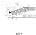
FIG. 3 is a partial enlarged view of the structure in the bonding area and the fan-out area of the display area shown inFIG. 2 . -
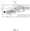
FIG. 4 is a partial enlarged view of the structure in the bonding area and the fan-out area of the display area according to another display panel of the present disclosure. -
FIG. 5 is a schematic diagram of a planar structure according to a driver chip of the present disclosure. - The technical solutions in the embodiments of the present disclosure will be clearly and completely described below in conjunction with the accompanying drawings in the embodiments of the present disclosure. Obviously, the described embodiments are only a part of the embodiments of the present disclosure, rather than all the embodiments. Based on the embodiments of the present disclosure, all other embodiments obtained by those skilled in the art without creative work shall fall within the protection scope of the present disclosure.
- In the description of the present disclosure, it should be understood that the directions or positional relationships indicated by the terms "upper", "lower", etc. are based on the directions or positional relationships shown in the drawings and are only for the convenience of describing the present disclosure and simplifying the description. It does not indicate or imply that the pointed device or element must have a specific orientation, be configured, and operated in a specific orientation, and therefore cannot be understood as a limitation of the present disclosure. In addition, the terms "first" and "second" are only used for descriptive purposes and cannot be understood as indicating or implying relative importance or implicitly indicating the number of indicated technical features. Therefore, the features defined with "first" and "second" may explicitly or implicitly include one or more of the features. In the description of the present disclosure, "plurality" means two or more, unless otherwise specifically defined.
- The present disclosure may repeat reference numbers and/or reference letters in different implementations. Such repetition is for the purpose of simplification and clarity and does not indicate the relationship between the various embodiments and/or settings discussed.
- The fan-out wiring area of the existing high-resolution display panel occupies a large space in the lower bezel of the display panel, which is not conducive to the technical problem of realizing the narrow-bezel full-screen design of the display panel. The present disclosure provides the first and/or second oblique bonding area, the first and/or second oblique bonding area are oblique relative to the horizontal bonding area, and the distance from the second end from the horizontal bonding area to the fan-out area is greater than the distance from the first end of the horizontal bonding area to the fan-out area. A part of each of the fan-out wires may extend into the first bonding area, so that a part of the fan-out area overlaps the bonding area and the height of the fan-out area along the first direction is shortened. The second bonding area is arranged in the area enclosed by the first and/or second oblique bonding area and the horizontal bonding area and the height of the bonding area in the first direction may be shortened. Therefore, the overall height of the fan-out area and the bonding area in the first direction is shortened, and the lower bezel of the display panel may be reduced. Under the premise of meeting the high resolution pursued by the market and not reducing the performance of the driver chip, an extremely narrow bezel design is realized. The first bonding terminals in each row in each of bonding terminal groups are arranged obliquely from the fourth end to the third end, so as to leave more wiring space for the fan-out wiring. The layout design of each structure of the bonding area and the fan-out area is further optimized, thereby improving the space utilization rate of the non-display area and realizing an extremely narrow bezel design. The first and/or second oblique bonding area includes a plurality of bonding terminal groups. The layout design of each structure of the bonding area and the fan-out area may be optimized by adjusting the interval between adjacent bonding terminal groups, and the wire width of the fan-out area wires may be increased. Therefore, the signal wire impedance is reduced, and the risk of the signal wire being too thin and broken is reduced to achieve a better display effect.
- The display panel, display device, and driver chip of the present disclosure are described in detail below in conjunction with specific embodiments.
- Referring to
FIG. 1 , a first embodiment of the present disclosure provides adisplay device 100 including adisplay panel 110, at least onedriver chip 120, and at least oneflexible circuit board 130. Thedriver chip 120 is formed on thedisplay panel 110 and is electrically connected to thedisplay panel 110, and theflexible circuit board 130 is located on a side of thedisplay panel 110 and is electrically connected to thedisplay panel 110. - Wherein the
display panel 110 includes adisplay area 101 and anon-display area 102 surrounding thedisplay area 101. - Wherein, a direction defined from the
display area 101 to thenon-display area 102 is a first direction D1. Thedisplay area 101 includes a plurality ofsignal wires 1011 extending along the first direction D1 and arranged along the second direction D2. The first direction D1 is perpendicular to the second direction D2. - Wherein, the
signal wires 1011 may be a data line for charging pixels (not shown) in thedisplay area 101 or one or two of touch signal wires connected to a touch sensor in thedisplay area 101. - Wherein, the
non-display area 102 includes a fan-outarea 10 and abonding area 20. Thebonding area 20 is located on a side of the fan-outarea 10 away from thedisplay area 101. - Wherein, the fan-out
area 10 includes a plurality of fan-outwires 11 extending along the first direction D1 as a whole and arranged along the second direction D2. One end of each of fan-outwires 11 is electrically connected to thecorresponding signal wires 1011. - Referring to
FIG. 2 , thebonding area 20 includes afirst bonding area 21 and asecond bonding area 22, and thefirst bonding area 21 and thesecond bonding area 22 are arranged along the first direction D1. Specifically, thefirst bonding area 21 is adjacent to the fan-outarea 10, and thesecond bonding area 22 is away from the fan-outarea 10. - Wherein, the
first bonding area 21 includes a firstoblique bonding area 211 and a secondoblique bonding area 213. The firstoblique bonding area 211 and the secondoblique bonding area 213 extend along thehorizontal bonding area 212 along the second direction D2 and are located at the end of thehorizontal bonding area 212. Specifically, the firstoblique bonding area 211 and the secondoblique bonding area 213 are axially symmetrically arranged at two ends of thehorizontal bonding area 212. - The first
oblique bonding area 211 includes afirst end 211a connected to thehorizontal bonding area 212 and asecond end 211b away from thehorizontal bonding area 212. In the second direction D2, the distance from thesecond end 211b to thedisplay area 101 is greater than the distance from thefirst end 211a to thedisplay area 101. a projection of the firstoblique bonding area 211 on thedisplay area 101 is located outside a projection of thehorizontal bonding area 212 on thedisplay area 101. Therefore, a part of each of fan-outwires 11 may extend into thefirst bonding area 21, so that a part of the fan-outarea 10 overlaps thebonding area 20, and the height of the fan-outarea 10 in the first direction D1 is shortened. The overall height of the fan-outarea 10 and thebonding area 20 in the first direction D1 is shortened, so that the lower bezel of thedisplay panel 110 may be reduced. Under the premise of meeting the high resolution pursued by the market and not reducing the performance of the driver chip, an extremely narrow bezel design is realized. - In an optional embodiment of the present disclosure, the
second bonding area 22 is arranged in an area enclosed by the firstinclined bonding area 211, the secondoblique bonding area 213, and thehorizontal bonding area 212. Thus, the layout of thefirst bonding area 21 and thesecond bonding area 22 in thebonding area 20 may be achieved. - In other embodiments, the
first bonding area 21 may also not include the secondoblique bonding zone 213. In this case, thesecond bonding area 22 is arranged in an area enclosed by the firstoblique bonding area 211 and thehorizontal bonding area 212. - Referring to
FIG. 2 to FIG. 4 , the firstoblique bonding area 211 includes a plurality of bonding terminal groups arranged in a stepped-shape manner. In this case, the layout design of each structure of the bonding area and the fan-out area may be optimized by adjusting the interval between adjacent bonding terminal groups. It is also possible to increase the wires width of the wires in the fan-out area, thereby reducing the impedance of the signal wire, and reducing the risk of the signal wire being too thin and broken, so as to achieve a better display effect. - Each of the bonding terminal groups includes a plurality of
first bonding terminals 2111. Thefirst bonding terminals 2111 in each of the bonding terminal groups are distributed in rows, and thefirst bonding terminals 2111 in adjacent rows are arranged alternately. Thehorizontal bonding area 212 includes a plurality ofsecond bonding terminals 2121. Thesecond bonding terminals 2121 are arranged in rows and thesecond bonding terminals 2121 are arranged horizontally in each of rows. Thesecond bonding terminals 2121 in two adjacent rows are arranged alternately. A part of the fan-outwires 11 extend into thefirst bonding area 21 and are electrically connected to thefirst bonding terminal 2111 and thesecond bonding terminal 2121 respectively. - Referring to
FIG. 2 andFIG. 3 , in an optional embodiment of the present disclosure, a plurality of the bonding terminal groups are arranged in a stepped-shape manner at equal intervals in the second direction D2. - Referring to
FIG. 4 , in an optional embodiment of the present disclosure, a plurality of the bonding terminal groups are arranged in a stepped-shape manner at unequal intervals in the second direction D2. - The plurality of bonding terminal groups may also be arranged at equal intervals or unequal intervals in the first direction D1.
- Referring to
FIG. 2 to FIG. 4 , in an optional embodiment of the present disclosure, two adjacent bonding terminal groups may partially overlap. In another optional embodiment of the present disclosure, two adjacent bonding terminal groups may not overlap. - Referring
FIG. 2 , a highest point of an end of each of the bonding terminal groups facing the fan-outarea 10 is defined as an apex of the bonding terminal group, a wire connecting an apex of the bonding terminal group at thesecond end 211b and an apex of the bonding terminal group at the first end forms an oblique angle θ1 in the second direction D2, and the oblique angle θ1 is an obtuse angle. Preferably, 100°≤θ1≤179°. - Referring to
FIG. 3 andFIG. 4 , a wire connecting the apices of the first bonding terminals at a same position in the two adjacent bonding terminal groups forms an oblique angle θ2 in the second direction, and the oblique angle θ2 is an acute angle. Preferably, 10°≤θ2≤85°. - Specifically, in
FIG. 3 , since the plurality of the bonding terminal groups are arranged in the stepped-shape manner at equal intervals in the second direction D2, the oblique angle θ2 of the wire connecting the apex centers of the first bonding terminals at the same position in the two adjacent bonding terminal groups in the second direction D2 is equal. - Specifically, in
FIG. 4 , since the plurality of the bonding terminal groups are arranged in the stepped-shape manner at unequal intervals in the second direction D2, the oblique angle θ2 of the wire connecting the apex centers of the first bonding terminals at the same position in the two adjacent bonding terminal groups in the second direction D2 may not be equal, or one part of them may be equal and the other part may be unequal. - Specifically, refer to
FIG. 3 to FIG. 4 , in the embodiment, the firstoblique bonding area 211 includes four firstbonding terminal groups 201. - The following will take the first
bonding terminal groups 201 as an example to specifically describe the arrangement of thefirst bonding terminals 2111 in each of bonding terminal groups. - Specifically, refer to
FIG. 3 , each of the bondingterminal groups 201 comprises athird end 2011 and afourth end 2012. In the second direction D2, thethird end 2011 is close to thehorizontal bonding area 212. Thefourth end 2012 is away from thehorizontal bonding area 212. In the first direction D1, a distance from thethird end 2011 to thedisplay area 101 is greater than a distance from thefourth end 2012 to thedisplay area 101. The plurality of thefirst bonding terminals 2111 in a same row are arranged obliquely from thefourth end 2012 to thethird end 2011. Thefirst bonding terminals 2111 of the firstbonding terminal group 201 are distributed in two rows and thefirst bonding terminals 2111 in the first row and thefirst bonding terminals 2111 in the second row are alternately arranged. That is, one of thefirst bonding terminals 2111 in the second row faces the gap between the twofirst bonding terminals 2111 in the first row. - Referring to
FIG. 2 , the secondoblique bonding area 213 includes a plurality of secondbonding terminal groups 205. Each of the secondbonding terminal groups 205 includes a plurality ofthird bonding terminals 2131. The plurality ofthird bonding terminals 2131 are distributed in rows, and thethird bonding terminals 2131 in adjacent rows are arranged alternately. - Referring to
FIG. 1 andFIG. 5 , Thedriver chip 120 at least includes ahorizontal terminal area 41, a firstoblique terminal area 42, and a secondoblique terminal area 43, wherein the firstoblique terminal area 42 and the secondoblique terminal area 43 are located at an end of thehorizontal terminal area 41 and oblique relative to thehorizontal terminal area 41. The firstoblique terminal area 42 and the secondoblique terminal area 43 extend obliquely along the first direction D1. Thehorizontal terminal area 41 extends horizontally along the second direction D2 perpendicular to the first direction D1. The secondoblique terminal area 43 and the firstoblique terminal area 42 are axially symmetrically arranged at two ends of thehorizontal terminal area 41. - The first
oblique terminal area 42 includes afifth end 422 connected to thehorizontal terminal area 41 and asixth end 423 away from thehorizontal terminal area 41. In the first direction D1, a projection of the firstoblique terminal area 42 on an extended area of thehorizontal terminal area 41 is located outside thehorizontal terminal area 41. The plurality of firstdriver terminal groups 421 are arranged in a stepped-shape manner at equal intervals or unequal intervals. - The first
oblique terminal area 42 includes a plurality of firstdriver terminal groups 421, and each of the firstdriver terminal groups 421 includes a plurality offirst driver terminals 4211. Thehorizontal terminal area 41 includes a plurality ofsecond driver terminals 4111. The secondoblique terminal area 43 includes a plurality of thirddriver terminal groups 431. Each of the seconddriver terminal groups 431 includes a plurality ofthird driver terminals 4311. Thefirst driver terminal 4211, thesecond driver terminal 4111, and thethird driver terminal 4311 are electrically connected to thefirst bonding terminal 2111, thesecond bonding terminal 2121, and thethird bonding terminal 2131, respectively. - Each of the first
driver terminal groups 421 comprises aseventh end 421a and aneighth end 421b. In the second direction D2, theseventh end 421a is close to thehorizontal terminal area 41 and theeighth end 421b is away from thehorizontal terminal area 41. In the second direction D2, the plurality offirst driver terminals 4211 in a same row are arranged obliquely from theeighth end 421b to theseventh end 421a. A vertical distance from theseventh end 421a to the extended area ofhorizontal terminal area 41 is less than a vertical distance from theeighth end 421b to the extended area of thehorizontal terminal area 41. - A highest point of the
eighth end 421b of each of the firstdriver terminal groups 421 is defined as an apex of the firstdriver terminal group 421, a wire connecting an apex of the firstdriver terminal group 421 at thesixth end 423 and an apex of the firstdriver terminal group 421 at thefifth end 422 forms an oblique angle in the first direction D1, and the oblique angle is an obtuse angle and greater than or equal to 100° and less than or equal to 179°. - A wire connecting the apices of the
first driver terminals 4211 at a same position in the two adjacentdriver terminal groups 421 forms an oblique angle in the second direction D2, and the oblique angle is an acute angle and greater than or equal to 10° and less than or equal to 85°. - Two adjacent first
driver terminal groups 421 are partially overlapped, thefirst driver terminals 4211 in each of the firstdriver terminal groups 421 are distributed in rows, and thefirst driver terminals 4211 in adjacent rows are arranged alternately. - The second
oblique terminal area 43 includes a plurality ofthird driver terminals 4311. The plurality ofthird driver terminals 4311 are distributed in rows, and thethird driver terminals 4311 in adjacent rows are arranged alternately. - The beneficial effects of the present disclosure: (1) the present disclosure provides the first and/or second oblique bonding area, the first and/or second oblique bonding area are oblique relative to the horizontal bonding area, and the distance from the second end from the horizontal bonding area to the fan-out area is greater than the distance from the first end of the horizontal bonding area to the fan-out area. A part of each of the fan-out wires may extend into the first bonding area, so that a part of the fan-out area overlaps the bonding area and the height of the fan-out area along the first direction is shortened. The second bonding area is arranged in the area enclosed by the first and/or second oblique bonding area and the horizontal bonding area and the height of the bonding area in the first direction may be shortened. Therefore, the overall height of the fan-out area and the bonding area in the first direction is shortened, and the lower bezel of the display panel may be reduced. Under the premise of meeting the high resolution pursued by the market and not reducing the performance of the driver chip, an extremely narrow bezel design is realized. (2) The first bonding terminals in each row in each of bonding terminal groups are arranged obliquely from the fourth end to the third end, so as to leave more wiring space for the fan-out wiring. The layout design of each structure of the bonding area and the fan-out area is further optimized, thereby improving the space utilization rate of the non-display area and realizing an extremely narrow bezel design. (3) The first and/or second oblique bonding area includes a plurality of bonding terminal groups. The layout design of each structure of the bonding area and the fan-out area may be optimized by adjusting the interval between adjacent bonding terminal groups, and the wire width of the fan-out area wiring may be increased. Therefore, the signal wire impedance is reduced, and the risk of the signal wire being too thin and broken is reduced to achieve a better display effect. (4) The second bonding area is arranged in an area enclosed by the first and/or second oblique bonding area and the horizontal bonding zone. The layout of the first bonding area and the second bonding area in the bonding area may be optimized
- In summary, although the present disclosure has been disclosed as above in preferred embodiments, said preferred embodiments are not intended to limit the present disclosure. Those of ordinary skill in the art may make various changes and modifications without departing from the spirit and scope of the present disclosure. Therefore, the protection scope of the present disclosure is subject to the scope defined by the claims.
Claims (20)
- A display panel, comprising a display area and a non-display area, wherein a direction from the display area to the non-display area is defined as a first direction and the non-display area comprises:a bonding area including a first bonding area and a second bonding area arranged along the first direction;wherein the first bonding area comprises a horizontal bonding area extending along a second direction and a first oblique bonding area, the first oblique bonding area is located at an end of the horizontal bonding area and oblique relative to the horizontal bonding area, and the first direction is perpendicular to the second direction;the first oblique bonding area comprises a first end connected to the horizontal bonding area and a second end away from the horizontal bonding area; in the second direction, a distance from the second end to the display area is greater than a distance from the first end to the display area, and a projection of the first oblique bonding area on the display area is located outside a projection of the horizontal bonding area on the display area; andthe first oblique bonding area comprises a plurality of bonding terminal groups, and the plurality of bonding terminal groups are arranged in a stepped-shape manner at equal intervals or unequal intervals.
- The display panel according to claim 1, wherein each of the bonding terminal groups comprises a plurality of first bonding terminals; each of the bonding terminal groups comprises a third end and a fourth end; in the second direction, the third end is close to the horizontal bonding area, and the fourth end is away from the horizontal bonding area; the plurality of the first bonding terminals in a same row are arranged obliquely from the fourth end to the third end, and a distance from the third end to the display area is greater than a distance from the fourth end to the display area.
- The display panel according to claim 2, wherein the non-display area further comprises a fan-out area, the first bonding area and the second bonding area are located on a side of the fan-out area away from the display area, the first bonding area is located between the fan-out area and the second bonding area, and the fan-out area comprises a plurality of fan-out wires; the horizontal bonding area comprises a plurality of second bonding terminals, and a part of the fan-out wires extend into the first bonding area and are electrically connected to the first bonding terminals and the second bonding terminals, respectively.
- The display panel according to claim 3, wherein a highest point of an end of each of the bonding terminal groups facing the fan-out area is defined as an apex of the bonding terminal group, a wire connecting an apex of the bonding terminal group at the second end and an apex of the bonding terminal group at the first end forms an oblique angle θ1 in the second direction, and the oblique angle θ1 is an obtuse angle.
- The display panel according to claim 4, wherein 100°≤θ1≤179°.
- The display panel according to claim 2, wherein a wire connecting the apices of the first bonding terminals at a same position in the two adjacent bonding terminal groups forms an oblique angle θ2 in the second direction, and the oblique angle θ2 is an acute angle.
- The display panel according to claim 6, wherein 10°≤θ2≤85°.
- The display panel according to claim 1, wherein the second bonding area is arranged in an area enclosed by the first oblique bonding area and the horizontal bonding area.
- The display panel according to claim 1, wherein two adjacent bonding terminal groups are partially overlapped.
- The display panel according to claim 2, wherein the first bonding terminals in each of the bonding terminal groups are distributed in rows and the first bonding terminals in adjacent rows are arranged alternately.
- The display panel according to claim 1, wherein the display panel further comprises a second oblique bonding area, and the second oblique bonding area and the first oblique bonding area are arranged axially symmetrically at two ends of the horizontal bonding area.
- The display panel according to claim 2, wherein the display panel further comprises a driver chip;
the driver chip at least comprises a horizontal terminal area and an oblique terminal area, the oblique terminal area is located at an end of the horizontal terminal area and oblique relative to the horizontal terminal area; the oblique terminal area comprises a plurality of first driver terminals, and the plurality of first driver terminals form a plurality of first driver terminal groups; an arrangement of the first driver terminals and the first driver terminal groups is the same as an arrangement of the first bonding terminals and the first bonding terminal groups, and the first driver terminals are electrically connected to the first bonding terminals. - A display device, comprising:
a display panel of claim 1. - The display device according to claim 13, wherein the display device further comprises a flexible circuit board electrically connected to the second bonding area.
- A driver chip, comprising:a horizontal terminal area and a first oblique terminal area, wherein the first oblique terminal area is located at an end of the horizontal terminal area and oblique relative to the horizontal terminal area;wherein the first oblique terminal area extends obliquely in a first direction, the horizontal terminal area extends horizontally in a second direction perpendicular to the first direction, and the first oblique terminal area comprises a plurality of first driver terminal groups;the first oblique terminal area comprises a fifth end connected to the horizontal terminal area and a sixth end away from the horizontal terminal area, a projection of the first oblique terminal area on an extended area of the horizontal terminal area is located outside the horizontal terminal area; the plurality of first driver terminal groups are arranged in a stepped-shape manner at equal intervals or unequal intervals.
- The driver chip according to claim 15, wherein each of the first driver terminal groups comprise a plurality of first driver terminals; each of the first driver terminal groups comprises a seventh end and an eighth end; in the second direction, the seventh end is close to the horizontal terminal area and the eighth end is away from the horizontal terminal area; in the first direction, the plurality of first driver terminals in a same row are arranged obliquely from the eighth end to the seventh end, a vertical distance from the seventh end to the extended area of horizontal terminal area is less than a vertical distance from the eighth end to the extended area of the horizontal terminal area.
- The driver chip according to claim 16, wherein a highest point of the eighth end of each of the first driver terminal groups is defined as an apex of the first driver terminal group, a wire connecting an apex of the first driver terminal group at the sixth end and an apex of the first driver terminal group at the fifth end forms an oblique angle in the second direction, and the oblique angle is an obtuse angle and greater than or equal to 100° and less than or equal to 179°.
- The driver chip according to claim 16, wherein a wire connecting the apices of the first driver terminals at a same position in the two adjacent driver terminal groups forms an oblique angle in the second direction, and the oblique angle is an acute angle and greater than or equal to 10° and less than or equal to 85°.
- The driver chip according to claim 16, wherein two adjacent first driver terminal groups are partially overlapped, the first driver terminals in each of the first driver terminal groups are distributed in rows, and the first driver terminals in adjacent rows are arranged alternately.
- The driver chip according to claim 15, wherein the driver chip further comprises a second oblique terminal area, and the second oblique terminal area and the first oblique terminal area are arranged axially symmetrically at two ends of the horizontal bonding area.
Applications Claiming Priority (2)
| Application Number | Priority Date | Filing Date | Title |
|---|---|---|---|
| CN202110676723.3A CN113362716B (en) | 2021-06-17 | 2021-06-17 | Display panel, display device and driver chip |
| PCT/CN2021/108466 WO2022262079A1 (en) | 2021-06-17 | 2021-07-26 | Display panel, display apparatus and driver chip |
Publications (2)
| Publication Number | Publication Date |
|---|---|
| EP4358072A1 true EP4358072A1 (en) | 2024-04-24 |
| EP4358072A4 EP4358072A4 (en) | 2025-05-14 |
Family
ID=77534893
Family Applications (1)
| Application Number | Title | Priority Date | Filing Date |
|---|---|---|---|
| EP21814661.1A Pending EP4358072A4 (en) | 2021-06-17 | 2021-07-26 | DISPLAY BOARD, DISPLAY DEVICE AND DRIVER CHIP |
Country Status (6)
| Country | Link |
|---|---|
| US (1) | US12336099B2 (en) |
| EP (1) | EP4358072A4 (en) |
| JP (1) | JP7405859B2 (en) |
| KR (1) | KR102669341B1 (en) |
| CN (1) | CN113362716B (en) |
| WO (1) | WO2022262079A1 (en) |
Families Citing this family (8)
| Publication number | Priority date | Publication date | Assignee | Title |
|---|---|---|---|---|
| CN113823241B (en) | 2021-09-30 | 2022-09-27 | 武汉华星光电技术有限公司 | Drive chip and display panel |
| US12471220B2 (en) * | 2021-11-01 | 2025-11-11 | BOE MLED Technology Co., Ltd. | Display module and method for manufacturing the same, and display device |
| CN114512057B (en) * | 2022-02-09 | 2024-01-09 | 武汉华星光电技术有限公司 | Display panel |
| CN115224512A (en) * | 2022-07-28 | 2022-10-21 | 维沃移动通信有限公司 | Display panels and electronic equipment |
| CN115731815B (en) * | 2022-11-11 | 2025-05-23 | 武汉华星光电技术有限公司 | Display panel and display device |
| CN116844418B (en) * | 2023-07-27 | 2026-07-03 | 京东方科技集团股份有限公司 | Display panel and display device |
| WO2025058448A1 (en) * | 2023-09-12 | 2025-03-20 | 주식회사 엘엑스세미콘 | Display device |
| CN119110653A (en) * | 2024-09-02 | 2024-12-10 | 京东方科技集团股份有限公司 | Display module and display device |
Family Cites Families (14)
| Publication number | Priority date | Publication date | Assignee | Title |
|---|---|---|---|---|
| KR100487355B1 (en) * | 2001-12-17 | 2005-05-03 | 엘지.필립스 엘시디 주식회사 | Electro-optics display device integrated touch paenl and bingding method thereof |
| JP3757923B2 (en) * | 2002-09-20 | 2006-03-22 | セイコーエプソン株式会社 | Electronics |
| JP3628676B2 (en) * | 2002-10-28 | 2005-03-16 | シャープ株式会社 | Display device |
| CN101009779B (en) * | 2006-01-24 | 2010-06-16 | 采钰科技股份有限公司 | Image sensing module for high-precision imaging control |
| KR20080049912A (en) * | 2006-12-01 | 2008-06-05 | 엘지디스플레이 주식회사 | Drive circuit device and display device having same |
| CN106293252B (en) * | 2016-09-09 | 2020-02-07 | 上海中航光电子有限公司 | Array substrate and display device |
| KR102777195B1 (en) * | 2016-10-13 | 2025-03-06 | 삼성디스플레이 주식회사 | Organic light emitting display device |
| CN210181359U (en) * | 2019-04-15 | 2020-03-24 | 武汉华星光电技术有限公司 | Display panel |
| CN111383554B (en) | 2019-11-06 | 2021-12-17 | 上海中航光电子有限公司 | Display panel and display device |
| CN110993676B (en) * | 2019-12-20 | 2022-06-03 | 厦门天马微电子有限公司 | Display panel and display device |
| CN111653200B (en) | 2020-06-29 | 2022-05-13 | 上海中航光电子有限公司 | Array substrate, display panel and display device |
| CN112037649B (en) * | 2020-08-12 | 2025-07-15 | 上海中航光电子有限公司 | Display panel and display device |
| CN111916019B (en) * | 2020-08-26 | 2022-11-01 | 上海中航光电子有限公司 | Driver chip and display device |
| CN112150933A (en) | 2020-10-28 | 2020-12-29 | 天马微电子股份有限公司 | Display panel and display device |
-
2021
- 2021-06-17 CN CN202110676723.3A patent/CN113362716B/en active Active
- 2021-07-26 JP JP2021548651A patent/JP7405859B2/en active Active
- 2021-07-26 KR KR1020217037353A patent/KR102669341B1/en active Active
- 2021-07-26 EP EP21814661.1A patent/EP4358072A4/en active Pending
- 2021-07-26 US US17/610,710 patent/US12336099B2/en active Active
- 2021-07-26 WO PCT/CN2021/108466 patent/WO2022262079A1/en not_active Ceased
Also Published As
| Publication number | Publication date |
|---|---|
| US12336099B2 (en) | 2025-06-17 |
| EP4358072A4 (en) | 2025-05-14 |
| KR102669341B1 (en) | 2024-05-27 |
| CN113362716B (en) | 2022-08-05 |
| JP2023534081A (en) | 2023-08-08 |
| US20240422909A1 (en) | 2024-12-19 |
| WO2022262079A1 (en) | 2022-12-22 |
| KR20220169374A (en) | 2022-12-27 |
| JP7405859B2 (en) | 2023-12-26 |
| CN113362716A (en) | 2021-09-07 |
Similar Documents
| Publication | Publication Date | Title |
|---|---|---|
| US12336099B2 (en) | Display panel, display device, and driver chip | |
| US11624956B2 (en) | Display panel and display device | |
| US11469257B2 (en) | Display panel and display device | |
| CN112037649B (en) | Display panel and display device | |
| CN108958539B (en) | Touch display panel and touch display device | |
| US11092860B1 (en) | Display panel and display device | |
| US20220107706A1 (en) | Display panel and display device | |
| CN108376522B (en) | Special-shaped display panel and display device | |
| US12471369B2 (en) | Display panel and display device | |
| US20210357059A1 (en) | Touch panel and display device | |
| CN106444182A (en) | Array substrate and display panel | |
| CN111323977A (en) | Display panel and display device | |
| US12229376B2 (en) | Touch-control display panel, touch-control display apparatus and method for manufacturing touch-control layer | |
| WO2023004842A1 (en) | Display panel and mobile terminal | |
| US12468200B1 (en) | Display panel and display apparatus | |
| US12292660B2 (en) | Display module with circuit boards | |
| US10691256B2 (en) | Touch substrate and touch device with reduced number of signal lines | |
| CN115280266B (en) | Array substrate, touch display device | |
| CN115542604B (en) | Curved surface display panel and display device | |
| CN111429829A (en) | Display panel | |
| CN111968528A (en) | Display panel and display device | |
| CN112162659A (en) | Touch module, touch display screen and electronic equipment | |
| US11853502B1 (en) | Display panel and display device having touch electrode connecting pads disposed in arc shape | |
| CN113655903B (en) | Display panel and display device | |
| EA046000B1 (en) | DISPLAY PANEL, DISPLAY DEVICE AND DRIVER IC |
Legal Events
| Date | Code | Title | Description |
|---|---|---|---|
| STAA | Information on the status of an ep patent application or granted ep patent |
Free format text: STATUS: UNKNOWN |
|
| STAA | Information on the status of an ep patent application or granted ep patent |
Free format text: STATUS: THE INTERNATIONAL PUBLICATION HAS BEEN MADE |
|
| PUAI | Public reference made under article 153(3) epc to a published international application that has entered the european phase |
Free format text: ORIGINAL CODE: 0009012 |
|
| STAA | Information on the status of an ep patent application or granted ep patent |
Free format text: STATUS: REQUEST FOR EXAMINATION WAS MADE |
|
| 17P | Request for examination filed |
Effective date: 20211206 |
|
| AK | Designated contracting states |
Kind code of ref document: A1 Designated state(s): AL AT BE BG CH CY CZ DE DK EE ES FI FR GB GR HR HU IE IS IT LI LT LU LV MC MK MT NL NO PL PT RO RS SE SI SK SM TR |
|
| DAV | Request for validation of the european patent (deleted) | ||
| DAX | Request for extension of the european patent (deleted) | ||
| REG | Reference to a national code |
Ref country code: DE Ref legal event code: R079 Free format text: PREVIOUS MAIN CLASS: G09F0009300000 Ipc: H10K0059131000 |
|
| A4 | Supplementary search report drawn up and despatched |
Effective date: 20250416 |
|
| RIC1 | Information provided on ipc code assigned before grant |
Ipc: H10D 86/60 20250101ALI20250410BHEP Ipc: H10D 86/40 20250101ALI20250410BHEP Ipc: G02F 1/1345 20060101ALI20250410BHEP Ipc: H10K 59/131 20230101AFI20250410BHEP |