EP4357669A1 - On-vehicle illumination device and production method therefor - Google Patents
On-vehicle illumination device and production method therefor Download PDFInfo
- Publication number
- EP4357669A1 EP4357669A1 EP22824822.5A EP22824822A EP4357669A1 EP 4357669 A1 EP4357669 A1 EP 4357669A1 EP 22824822 A EP22824822 A EP 22824822A EP 4357669 A1 EP4357669 A1 EP 4357669A1
- Authority
- EP
- European Patent Office
- Prior art keywords
- substrate
- illumination device
- light
- vehicle illumination
- wiring pattern
- Prior art date
- Legal status (The legal status is an assumption and is not a legal conclusion. Google has not performed a legal analysis and makes no representation as to the accuracy of the status listed.)
- Pending
Links
Images





Classifications
-
- F—MECHANICAL ENGINEERING; LIGHTING; HEATING; WEAPONS; BLASTING
- F21—LIGHTING
- F21S—NON-PORTABLE LIGHTING DEVICES; SYSTEMS THEREOF; VEHICLE LIGHTING DEVICES SPECIALLY ADAPTED FOR VEHICLE EXTERIORS
- F21S41/00—Illuminating devices specially adapted for vehicle exteriors, e.g. headlamps
- F21S41/10—Illuminating devices specially adapted for vehicle exteriors, e.g. headlamps characterised by the light source
- F21S41/14—Illuminating devices specially adapted for vehicle exteriors, e.g. headlamps characterised by the light source characterised by the type of light source
- F21S41/141—Light emitting diodes [LED]
- F21S41/155—Surface emitters, e.g. organic light emitting diodes [OLED]
-
- F—MECHANICAL ENGINEERING; LIGHTING; HEATING; WEAPONS; BLASTING
- F21—LIGHTING
- F21S—NON-PORTABLE LIGHTING DEVICES; SYSTEMS THEREOF; VEHICLE LIGHTING DEVICES SPECIALLY ADAPTED FOR VEHICLE EXTERIORS
- F21S41/00—Illuminating devices specially adapted for vehicle exteriors, e.g. headlamps
- F21S41/20—Illuminating devices specially adapted for vehicle exteriors, e.g. headlamps characterised by refractors, transparent cover plates, light guides or filters
- F21S41/285—Refractors, transparent cover plates, light guides or filters not provided in groups F21S41/24 - F21S41/2805
-
- B—PERFORMING OPERATIONS; TRANSPORTING
- B60—VEHICLES IN GENERAL
- B60Q—ARRANGEMENT OF SIGNALLING OR LIGHTING DEVICES, THE MOUNTING OR SUPPORTING THEREOF OR CIRCUITS THEREFOR, FOR VEHICLES IN GENERAL
- B60Q3/00—Arrangement of lighting devices for vehicle interiors; Lighting devices specially adapted for vehicle interiors
- B60Q3/50—Mounting arrangements
- B60Q3/54—Lighting devices embedded in interior trim, e.g. in roof liners
-
- F—MECHANICAL ENGINEERING; LIGHTING; HEATING; WEAPONS; BLASTING
- F21—LIGHTING
- F21S—NON-PORTABLE LIGHTING DEVICES; SYSTEMS THEREOF; VEHICLE LIGHTING DEVICES SPECIALLY ADAPTED FOR VEHICLE EXTERIORS
- F21S4/00—Lighting devices or systems using a string or strip of light sources
- F21S4/20—Lighting devices or systems using a string or strip of light sources with light sources held by or within elongate supports
- F21S4/22—Lighting devices or systems using a string or strip of light sources with light sources held by or within elongate supports flexible or deformable, e.g. into a curved shape
- F21S4/24—Lighting devices or systems using a string or strip of light sources with light sources held by or within elongate supports flexible or deformable, e.g. into a curved shape of ribbon or tape form, e.g. LED tapes
-
- F—MECHANICAL ENGINEERING; LIGHTING; HEATING; WEAPONS; BLASTING
- F21—LIGHTING
- F21S—NON-PORTABLE LIGHTING DEVICES; SYSTEMS THEREOF; VEHICLE LIGHTING DEVICES SPECIALLY ADAPTED FOR VEHICLE EXTERIORS
- F21S41/00—Illuminating devices specially adapted for vehicle exteriors, e.g. headlamps
- F21S41/10—Illuminating devices specially adapted for vehicle exteriors, e.g. headlamps characterised by the light source
- F21S41/14—Illuminating devices specially adapted for vehicle exteriors, e.g. headlamps characterised by the light source characterised by the type of light source
- F21S41/141—Light emitting diodes [LED]
- F21S41/143—Light emitting diodes [LED] the main emission direction of the LED being parallel to the optical axis of the illuminating device
-
- F—MECHANICAL ENGINEERING; LIGHTING; HEATING; WEAPONS; BLASTING
- F21—LIGHTING
- F21S—NON-PORTABLE LIGHTING DEVICES; SYSTEMS THEREOF; VEHICLE LIGHTING DEVICES SPECIALLY ADAPTED FOR VEHICLE EXTERIORS
- F21S41/00—Illuminating devices specially adapted for vehicle exteriors, e.g. headlamps
- F21S41/10—Illuminating devices specially adapted for vehicle exteriors, e.g. headlamps characterised by the light source
- F21S41/14—Illuminating devices specially adapted for vehicle exteriors, e.g. headlamps characterised by the light source characterised by the type of light source
- F21S41/141—Light emitting diodes [LED]
- F21S41/151—Light emitting diodes [LED] arranged in one or more lines
- F21S41/153—Light emitting diodes [LED] arranged in one or more lines arranged in a matrix
-
- F—MECHANICAL ENGINEERING; LIGHTING; HEATING; WEAPONS; BLASTING
- F21—LIGHTING
- F21S—NON-PORTABLE LIGHTING DEVICES; SYSTEMS THEREOF; VEHICLE LIGHTING DEVICES SPECIALLY ADAPTED FOR VEHICLE EXTERIORS
- F21S43/00—Signalling devices specially adapted for vehicle exteriors, e.g. brake lamps, direction indicator lights or reversing lights
- F21S43/10—Signalling devices specially adapted for vehicle exteriors, e.g. brake lamps, direction indicator lights or reversing lights characterised by the light source
- F21S43/13—Signalling devices specially adapted for vehicle exteriors, e.g. brake lamps, direction indicator lights or reversing lights characterised by the light source characterised by the type of light source
- F21S43/14—Light emitting diodes [LED]
-
- F—MECHANICAL ENGINEERING; LIGHTING; HEATING; WEAPONS; BLASTING
- F21—LIGHTING
- F21S—NON-PORTABLE LIGHTING DEVICES; SYSTEMS THEREOF; VEHICLE LIGHTING DEVICES SPECIALLY ADAPTED FOR VEHICLE EXTERIORS
- F21S43/00—Signalling devices specially adapted for vehicle exteriors, e.g. brake lamps, direction indicator lights or reversing lights
- F21S43/10—Signalling devices specially adapted for vehicle exteriors, e.g. brake lamps, direction indicator lights or reversing lights characterised by the light source
- F21S43/13—Signalling devices specially adapted for vehicle exteriors, e.g. brake lamps, direction indicator lights or reversing lights characterised by the light source characterised by the type of light source
- F21S43/14—Light emitting diodes [LED]
- F21S43/145—Surface emitters, e.g. organic light emitting diodes [OLED]
-
- F—MECHANICAL ENGINEERING; LIGHTING; HEATING; WEAPONS; BLASTING
- F21—LIGHTING
- F21V—FUNCTIONAL FEATURES OR DETAILS OF LIGHTING DEVICES OR SYSTEMS THEREOF; STRUCTURAL COMBINATIONS OF LIGHTING DEVICES WITH OTHER ARTICLES, NOT OTHERWISE PROVIDED FOR
- F21V31/00—Gas-tight or water-tight arrangements
- F21V31/04—Provision of filling media
-
- F—MECHANICAL ENGINEERING; LIGHTING; HEATING; WEAPONS; BLASTING
- F21—LIGHTING
- F21S—NON-PORTABLE LIGHTING DEVICES; SYSTEMS THEREOF; VEHICLE LIGHTING DEVICES SPECIALLY ADAPTED FOR VEHICLE EXTERIORS
- F21S43/00—Signalling devices specially adapted for vehicle exteriors, e.g. brake lamps, direction indicator lights or reversing lights
- F21S43/10—Signalling devices specially adapted for vehicle exteriors, e.g. brake lamps, direction indicator lights or reversing lights characterised by the light source
- F21S43/19—Attachment of light sources or lamp holders
- F21S43/195—Details of lamp holders, terminals or connectors
-
- F—MECHANICAL ENGINEERING; LIGHTING; HEATING; WEAPONS; BLASTING
- F21—LIGHTING
- F21Y—INDEXING SCHEME ASSOCIATED WITH SUBCLASSES F21K, F21L, F21S and F21V, RELATING TO THE FORM OR THE KIND OF THE LIGHT SOURCES OR OF THE COLOUR OF THE LIGHT EMITTED
- F21Y2115/00—Light-generating elements of semiconductor light sources
- F21Y2115/10—Light-emitting diodes [LED]
-
- H—ELECTRICITY
- H05—ELECTRIC TECHNIQUES NOT OTHERWISE PROVIDED FOR
- H05K—PRINTED CIRCUITS; CASINGS OR CONSTRUCTIONAL DETAILS OF ELECTRIC APPARATUS; MANUFACTURE OF ASSEMBLAGES OF ELECTRICAL COMPONENTS
- H05K2203/00—Indexing scheme relating to apparatus or processes for manufacturing printed circuits covered by H05K3/00
- H05K2203/11—Treatments characterised by their effect, e.g. heating, cooling, roughening
- H05K2203/1131—Sintering, i.e. fusing of metal particles to achieve or improve electrical conductivity
-
- H—ELECTRICITY
- H05—ELECTRIC TECHNIQUES NOT OTHERWISE PROVIDED FOR
- H05K—PRINTED CIRCUITS; CASINGS OR CONSTRUCTIONAL DETAILS OF ELECTRIC APPARATUS; MANUFACTURE OF ASSEMBLAGES OF ELECTRICAL COMPONENTS
- H05K2203/00—Indexing scheme relating to apparatus or processes for manufacturing printed circuits covered by H05K3/00
- H05K2203/13—Moulding and encapsulation; Deposition techniques; Protective layers
- H05K2203/1305—Moulding and encapsulation
- H05K2203/1316—Moulded encapsulation of mounted components
Definitions
- the present invention relates to a thin and threedimensionally molded on-vehicle illumination device.
- An on-vehicle illumination device such as a headlight and a rear lamp is configured by, for example, as disclosed in Patent Literature 1, fixing a light source unit, a reflector, and a projection lens unit into an opening of a housing by screwing or the like, and closing the opening with a cover.
- Each unit is configured by a plurality of parts and mechanisms, which are also structured to be assembled together by screwing, fitting, soldering, or the like.
- a fan is installed on a lamp housing to cool the light source unit by discharging air inside the lamp housing to the outside.
- the on-vehicle illumination device in the related art has a structure in which many parts are assembled, and a space is required in the housing. Therefore, the thickness of the entire on-vehicle illumination device increases, and the volume occupied by the entire on-vehicle illumination device increases.
- an on-vehicle illumination device is required to have high design quality that matches the outer appearance of a vehicle and to provide comfort by expanding the internal space of the vehicle.
- a three-dimensional shape with a complex curved surface and a compact structure are desired.
- An objective of the invention is to provide an on-vehicle illumination device which is compact and capable of realizing a complex curved surface shape.
- an on-vehicle illumination device includes a substrate, a wiring pattern mounted on the substrate, a light-emitting element disposed on the wiring pattern, and an outer lens layer made of a resin and mounted on the light-emitting element.
- the substrate has a shape curved along a curvature of the outer lens layer in a front-rear direction.
- a substrate has a shape curved along a curvature of an outer lens layer in a front-rear direction, it is possible to provide an on-vehicle illumination device which is compact and capable of realizing a complex curved surface shape.
- an on-vehicle illumination device is configured by a plurality of parts, and thus, a space is required therein to assemble the parts.
- the inventors provide an on-vehicle illumination device capable of reducing the number of parts by eliminating an internal space.
- a heating temperature of the resin required during insert molding is higher than a melting point of a solder such as a low melting point solder, a eutectic solder, and a lead-free solder. Therefore, during insert molding, the solder is remelted by heat of a molten resin, and a light-emitting element mounted on a substrate falls off.
- a solder such as a low melting point solder, a eutectic solder, and a lead-free solder. Therefore, during insert molding, the solder is remelted by heat of a molten resin, and a light-emitting element mounted on a substrate falls off.
- the inventors use fine metal particles as a bonding material for the light-emitting element, and make insert molding possible by using a melting point drop of the fine metal particles.
- the fine metal particles are melted at a low temperature to form a bulk, thereby achieving bonding.
- the bulk bonding material has a high melting point, and thus, the bonding material is not remelted even by the heat of the molten resin. Therefore, insert molding becomes possible.
- FIG. 1(a) is a perspective view of the on-vehicle illumination device 1 according to the present embodiment
- FIG. 1(b) is a cross-sectional view thereof
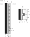
- FIG. 2(a) is a view schematically illustrating a cross-sectional structure of the on-vehicle illumination device 1
- FIG. 2(b) is a view obtained by enlarging a part of FIG. 1(a)
- FIG. 3 is a view illustrating an example of a part of a wiring pattern on a substrate.
- the on-vehicle illumination device 1 includes a substrate 10 and a wiring pattern 11 which is mounted on the substrate 10.
- Light-emitting elements 12 are disposed on the wiring pattern 11.
- a sealing resin layer 50 which covers the light-emitting elements 12 and covers the wiring pattern 11 and at least a part of an upper surface of the substrate 10, is disposed on the light-emitting elements 12.
- An outer lens layer 20 is disposed on the sealing resin layer 50.
- the wiring pattern 11 and electrodes of the light-emitting elements 12 are bonded by a bonding material 13.
- the bonding material 13 is a metal which is obtained by sintering metal particles.
- the outer lens layer 20 is integrated with the upper surface of the substrate 10, the light-emitting elements 12, and the wiring pattern 11 in close contact without a gap. Specifically, in the outer lens layer 20, a portion where the sealing resin layer 50 is disposed is in close contact with the sealing resin layer 50, and a portion where the sealing resin layer 50 is not disposed is in direct close contact with and integrated with the upper surface of the substrate 10, the light-emitting element 12, and the wiring pattern 11.
- the outer lens layer 20 is formed by insert molding using a pre-prepared mold in which a desired upper surface shape of the outer lens layer is formed. That is to say, the outer lens layer 20 is formed by disposing the substrate 10 on which the light-emitting elements 12 are mounted inside the mold, filling a resin in the mold, and curing the resin.
- the sintered metal particles are used as a bonding material, sintering can be performed at a relatively low temperature during bonding by photosintering or the like. Furthermore, since a bulk form is achieved through sintering, a melting point becomes higher than that of a solder. Therefore, even when the heat-molten resin is poured into a mold in insert molding or the like, the bonding material 13 is not remelted, and the outer lens layer 20 integrated with the light-emitting elements 12 and the substrate 10 can be formed.
- the on-vehicle illumination device 1 which does not have a space therein and is compact. Furthermore, since the on-vehicle illumination device 1 can be molded using a mold, it is also possible to form the outer lens layer 20 into a complex curved surface shape.
- An on-vehicle illumination device of FIG. 1 has a shape (a convex shape) which is curved in a front-rear direction and an up-down direction.
- the front-rear direction refers to a direction that coincides with a front-rear direction of a vehicle when the on-vehicle illumination device is installed on the vehicle.
- the substrate 10 is curved in the front-rear and up-down directions while being in close contact with the outer lens layer 20. In other words, the substrate 10 is curved in a shape which follows a curvature of the outer lens layer 20 in the front-rear direction and the up-down direction.
- the peripheries of the light-emitting elements 12 are sealed by the sealing resin layer 50, but the sealing resin layer 50 may not be provided.
- the outer lens layer 20 is in direct close contact with the light-emitting elements 12, the wiring pattern 11, and the upper surface of the substrate 10.
- the light-emitting element 12 may be an LED die which includes electrodes and a semiconductor layer including a light-emitting layer and does not include a package, an LED package in which an LED die is mounted on a submount substrate on which submount electrodes are formed and a sealing resin, a fluorescent layer, or a reflective resin layer is filled around the LED die as necessary, an element having a light receiving function, or a semiconductor laser element.
- the light-emitting element 12 is an LED package in which an LED die is mounted on a submount substrate on which submount electrodes are formed and a sealing resin, a fluorescent layer, or a reflective resin layer is filled around the LED die as necessary, as a die bonding material for bonding the submount electrodes and electrodes for the LED die, a metal obtained by sintering metal particles is used instead of using a solder.
- the electronic circuit elements 14 and 15 can be mounted on the wiring pattern 11.
- the electronic circuit elements 14 and 15 are an IC (integrated circuit) chip which drives the light-emitting elements 12 and a chip resistor, respectively.
- the outer lens layer 20 is integrated with the electronic circuit elements 14 and 15 in close contact without a gap.
- a metal obtained by sintering metal particles is used as a bonding material for bonding the electrodes of the electronic circuit elements 14 and 15 and the wiring pattern 11.
- Bonding may be performed by using oven heating such as reflow, direct heating with a heat tool, or heating by light such as a flash or a laser when the substrate 10 has optical transparency.
- oven heating such as reflow
- direct heating with a heat tool or heating by light such as a flash or a laser when the substrate 10 has optical transparency.
- light such as a flash or a laser when the substrate 10 has optical transparency.
- bonding by light in a production process, it is possible to perform irradiation with light from a rear surface side of the substrate 10 toward the position of the bonding material 13, heat the wiring pattern 11 and the bonding material 13 by light, and sinter the bonding material 13.
- a housing 30 having a shape which follows the substrate is in close contact with and fixed to a lower surface of the substrate 10.
- the housing 30 is curved in a shape which follows the curvatures (convex shape) of the substrate 10 and the outer lens layer 20 in the front-rear direction and the up-down direction, and is in close contact with the substrate 10 and the outer lens layer 20.
- a back surface of the housing 30 has a shape which follows the curvature of the outer lens layer 20 in the front-rear direction and the up-down direction.
- the on-vehicle illumination device 1 which is installed at the front of the vehicle, in a curved shape which is convex toward the front, a space which is surrounded by the curved shape of the on-vehicle illumination device 1 can be created on a back surface (rear side) of the on-vehicle illumination device 1 installed at the front of the vehicle.
- a space which is surrounded by the curved shape of the on-vehicle illumination device 1 can be created on the back surface (front side) of the on-vehicle illumination device 1 installed at the rear of the vehicle.
- a decorative film 40 such as a reflector which reflects light generated from the light-emitting elements 12 may be inserted between the substrate 10 and the housing 30.
- the upper surface of the decorative film 40 is in close contact with the lower surface of the substrate 10, and the lower surface of the decorative film 40 is in close contact with the upper surface of the housing 30.
- the decorative film 40 also has a shape which bulges in the front-rear direction and the up-down direction along the outer lens layer 20.
- a resin material such as highly heat-resistant PET (polyethylene terephthalate), PI (polyimide), and glass epoxy or a metal-based substrate such as an aluminum substrate can be used.
- a flexible material is used. It is desirable to select a material for the substrate 10, which has a melting point or a softening point higher than a temperature (150 to 320°C) when molding the outer lens layer 20 and which does not cause deformation or alteration during molding.
- the thickness of the substrate 10 is, for example, 25 um to 2 mm.
- the wiring pattern 11 can be formed by bonding a metal foil such as a copper foil to the substrate 10 and processing the metal foil into a shape of the wiring pattern 11.
- the wiring pattern 11 may be formed by forming a metal film on the substrate 10 by sputtering or the like and processing the metal film into the shape of the wiring pattern 11 by etching.
- the wiring pattern 11 may be formed by applying a conductive ink or the like onto the substrate 10 in the shape of the wiring pattern 11 and then heating and sintering the conductive ink.
- the thickness of the wiring pattern 11 is, for example, about 12 um to 35 ⁇ m.
- a technique such as gravure printing or screen printing can be used.
- the bonding material 13 and the wiring pattern 11 may be formed simultaneously by using a conductive ink in which metal particles are dispersed in a solvent.
- the metal foil is fixed to the substrate 10 by an adhesive.
- polyurethane ester type acrylic type, epoxy type, silicone type, or the like can be used.
- the thickness of the adhesive is, for example, 5 to 100 ⁇ m.
- a method of bonding the substrate 10 and the wiring pattern 11 with the adhesive a method such as dry lamination can be used.
- an adhesive sheet can also be used.
- bonding may be performed using thermocompression, lamination, or the like.
- the bonding material 13 is formed by sintering an ink or paste in which conductive metal nanoparticles are dispersed.
- composition of the conductive ink or paste is preferably in the range of 20 wt% to 95 wt% of conductive particles, 5 wt% to 70 wt% of a solvent, and 0.01 wt% to 10 wt% of an organic dispersant.
- conductive metals and a conductive metal oxide such as Au, Ag, Cu, Pd, ITO, Ni, Pt, and Fe can be used.
- a maximum value of the particle size distribution of the conductive particles is preferably 1 nm or more and 10 ⁇ m or less.
- glycol such as ethylene glycol, diethylene glycol, triethylene glycol, and polyethylene glycol
- diol such as propanediol, butanediol, and benzenediol
- triol such as glycerin
- ether such as diethyl ether and diphenyl ether
- irradiation with electromagnetic waves such as light
- electromagnetic waves such as light
- laser or flash heating can be used.
- the conductive ink or paste is formed using dispensing or screen printing, and the light-emitting elements 12 and the electronic circuit elements 14 and 15 are installed.
- the conductive ink or paste is heated to a temperature of 200 to 400°C to melt and sinter the conductive particles.
- a jig such as a collet may be used to fix or apply a load, or heating may be performed while applying a load.
- a resin which is transparent to light emitted by the light-emitting elements 12 is used as a material of the sealing resin layer 50.
- a resin which is transparent to light emitted by the light-emitting elements 12 is used.
- an epoxy, urethane-based resin, a silicone resin, or a modified resin as a combination thereof can be used.
- PMMA polymethyl methacrylate
- ABS acrylonitrile-butadienestyrene copolymer synthetic resin
- PP polypropylene
- PC polycarbonate
- PBT polybutylene terephthalate
- PES polyether sulfone
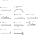
- FIGS. 4 and 5 An example of a production method according to the present embodiment will be described using FIGS. 4 and 5 .
- a polyimide film with a thickness of 25 um to 50 ⁇ m was prepared as the substrate 10.
- a copper foil with a thickness of 12 to 35 um configuring the wiring pattern 11 is bonded using an adhesive layer 16 as described above.
- the copper foil is patterned into a desired shape of the wiring pattern 11 by subtractive etching.
- a surface treatment layer 11a is formed on the surface of the copper foil.
- a Ni layer and an Au layer are sequentially formed as the surface treatment layer 11a by electroless Ni plating and electroless gold plating.
- the thickness of the Ni layer is 1 to 5 um, and the thickness of the Au layer is about 0.03 ⁇ m.
- a water-soluble preflux may be used.
- the above-mentioned conductive ink is prepared and applied to respective regions of the wiring pattern 11 where the electrodes of the light-emitting elements 12 and the electronic circuit elements 14 and 15 are mounted, to form a coating film 13a.
- the light-emitting elements 12 and the electronic circuit elements 14 and 15 are mounted on the coating film 13a of the conductive ink using a device. If necessary, while applying a load to the light-emitting elements 12 and the electronic circuit elements 14 and 15, irradiation with laser light from the rear surface side of the substrate 10 is performed. By this fact, the wiring pattern 11 is heated, and the conductive particles of the coating film 13a of the conductive ink are melted and sintered by heat transfer. The bonding material 13 for bonding the light-emitting elements 12 and the like and the wiring pattern 11 is formed.
- a resin such as a silicone resin is filled around the light-emitting elements 12 on the substrate 10 using dispense coating, a mold, or the like, and is heated and cured to form the sealing resin layer 50.
- the curing temperature of the resin is, for example, about 150°C, depending on a resin to be used.
- the sealing resin layer 50 may not be formed.
- the sealing resin layer 50 may be formed over the entire upper surface of the substrate 10 or may be partially formed.
- the decorative film 40 prepared in advance is bonded to a rear surface of the substrate 10 using an adhesive layer.
- a reflector is used as the decorative film 40.
- the adhesive used to bond the copper foil and the substrate 10 in the process of FIG. 4(a) can be used.
- the decorative film 40 may be formed on the lower surface of the substrate by printing.
- the stack which is manufactured in the processes of FIGS. 4(a) to 4(g) and in which the light-emitting elements 12 are mounted on the substrate 10 and the decorative film 40 is disposed on the rear surface of the substrate 10, is set inside molding molds 101a and 101b.
- three-dimensional forming may be performed to obtain a desired shape.
- a PC (polycarbonate) resin is heated to about 260 to 320°C.
- the molds 101a and 101b are heated to about 70 to 110°C.
- the heated and fluidic PC resin is injected into the molds 101a and 101b and is then cured, and thereby, the outer lens layer 20 having the desired shape is integrally formed by insert molding in close contact with the substrate 10, the light-emitting elements 12, the wiring pattern 11, and the like.
- the integrally molded product is removed from the molds 101a and 101b, and a nozzle mark 102 on the outer lens layer 20 is cut and removed.
- the housing 30 is bonded, by the above-described adhesive, to the rear surface of the substrate 10 of the molded product which is obtained in the process of FIG. 5(c) and in which the substrate 10 and the like and the outer lens layer 20 are integrally molded.
- the substrate 10 and the housing 30 may be fixed to each other by a fitting structure such as a snap fit, or may be formed by two-color molding or the like.
- the on-vehicle illumination device 1 according to the first embodiment can be produced.
- the on-vehicle illumination device 1 uses a conductive ink in which conductive nanoparticles are dispersed in a solvent, in order to form the bonding material 13 ( FIG. 4(d) ).
- a conductive ink in which conductive nanoparticles are dispersed in a solvent, in order to form the bonding material 13 ( FIG. 4(d) ).
- conductive nanoparticles can be sintered at a lower melting point than a normal bulk body ( FIG. 4(e) ).
- the conductive nanoparticles after sintering have properties close to those of a bulk, a melting point drop does not occur, and even at a high temperature when the outer lens layer 20 is molded using a mold, the conductive nanoparticles are not remelted, and mounted components (such as the light-emitting elements 12) do not fall off ( FIG. 5(b) ).
- the bonding material 13 which is a sintered body of conductive particles has the above-mentioned bulk properties, thermal and electrical properties are superior to a resin-curing type such as a silver paste.
- the on-vehicle illumination device 1 according to the first embodiment is thin because there is no internal space. Further, since there is no need for screwing or the like and the number of parts can be reduced compared to the related art, weight reduction and simplification are possible.
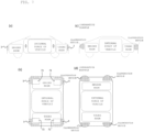
- FIGS. 7(a) and 7(b) are diagrams illustrating the internal space of a vehicle when the vehicle equipped with the on-vehicle illumination device 1 according to the first embodiment is viewed from the side and the top, respectively.
- FIGS. 7(c) and 7(b) are diagrams illustrating the internal space of a vehicle when the vehicle equipped with an illumination device in the related art is viewed from the side and the top, respectively.
- the on-vehicle illumination device 1 according to the first embodiment can reduce an installation space when being installed on a vehicle, compared to the illumination device in the related art of FIGS. 7(c) and 7(d) . Therefore, it becomes possible to effectively utilize the internal space of the vehicle.
- the back surface of the on-vehicle illumination device 1 since the back surface of the on-vehicle illumination device 1 itself has a curved shape which follows the shape of the curvature of the outer lens layer 20 in the front-rear direction and the up-down direction, as illustrated in FIG. 7(b) , a space 71 surrounded by the curved shape of the on-vehicle illumination device 1 is created on the back surface (rear side) of the on-vehicle illumination device 1 installed at the front of the vehicle. A space 72 surrounded by the curved shape of the on-vehicle illumination device 1 is created on the back surface (front side) of the on-vehicle illumination device 1 installed at the rear of the vehicle.
- the spaces 71 and 72 are spaces that are not present in a vehicle on which the illumination device in the related art is installed ( FIG. 7(d) ). Therefore, by installing the on-vehicle illumination device 1 according to the first embodiment, as illustrated in FIG. 7(c) , a part of an engine room or a trunk room of the vehicle may be disposed in the spaces 71 and 72 on the back surface of the on-vehicle illumination device 1 according to the first embodiment. Conversely, in the vehicle equipped with the illumination device in the related art, as can be clearly seen from FIG.
- the on-vehicle illumination device 1 according to the first embodiment can effectively utilize the internal space of the vehicle, compared to the illumination device in the related art.
- the on-vehicle illumination device 1 according to the first embodiment can be easily molded into a complex three-dimensional shape. Therefore, there is no need for a complicated assembly structure, and as illustrated in FIGS. 1(a) and 1(b) , it is possible to produce an on-vehicle illumination device with a curved shape relatively easily at low cost. Therefore, it is possible to produce a compact and low-cost on-vehicle illumination device having a high design quality with a curved surface matching the design of a vehicle.
- the process of FIG. 4(g) is not performed.
- the decorative film 40 is not provided.
- the processes of FIGS. 8(a) to 8(c) are performed using the substrate 10 obtained in FIG. 4(f) , to which the light-emitting elements 12 are bonded.
- FIGS. 8(a) to 8(c) are similar to FIGS. 5(a) to 5(c) of the first embodiment, but without the decorative film 40 obtained in FIG. 4(f) , a stack of the substrate 10, the light-emitting elements 12, and the like is disposed in the molds 101a and 101b, and a resin is filled in the molds 101a and 101b.
- the outer lens layer 20 with a desired shape is integrally formed by insert molding in close contact with the substrate 10, the light-emitting elements 12, the wiring pattern 11, and the like.
- the housing 30 is bonded to the lower surface of the substrate 10 in close contact without a gap.
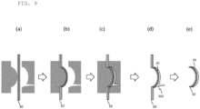
- FIGS. 9(a) to 9(d) a production method for a three-dimensional on-vehicle illumination device will be described using FIGS. 9(a) to 9(d) .
- molds 101a and 101b are formed in advance into a desired three-dimensional shape.
- the stack manufactured in the processes of FIGS. 4(a) to 4(g) of the first embodiment or the stack manufactured in the processes of FIGS. 4(a) to 4(f) is disposed inside the molds 101a and 101b.
- the light-emitting elements 12 are stacked on the substrate 10, and the decorative film is bonded to the lower surface of the substrate 10.
- the light-emitting elements 12 are stacked on the substrate 10, and a decorative film is not provided.
- the substrate 10 is inserted into the molds, the substrate 10 is softened by heating, and the shape of the stack is changed into a desired three-dimensional shape by vacuum molding, pressure molding, press molding, or the like.
- the process may be divided into two, and a complex shape can be formed by using not only heating but also vacuum forming. In this case, molds suitable for each process are used. In the case of one process, the upper molds of FIG. 9(b) and FIG. 9(c) are the same mold.
- the molds 101a and 101b are heated, and the heated and fluidic PC resin is injected into the molds 101a and 101b and is then cured.
- the outer lens layer 20 having a desired three-dimensional shape is integrally formed by insert molding in close contact with the substrate 10, the light-emitting elements 12, the wiring pattern 11, and the like.
- the integrally molded product is removed from the molds 101a and 101b, and the nozzle mark 102 is removed.
- the unnecessary portion is removed by cutting.
- the separately formed three-dimensional housing 30 is bonded to the lower surface of the three-dimensional substrate 10 in close contact without a gap.
- the substrate 10 can be changed into a three-dimensional shape, and at the same time, the outer lens layer 20 can be integrally molded into a shape which is in close contact with the substrate 10, so that a complex three-dimensional shape may be easily formed.
- the on-vehicle illumination device with a curved shape illustrated in FIGS. 1(a) and 1(b) can be relatively easily produced at low cost. Therefore, it is possible to produce, at low cost, an on-vehicle illumination device which is thin and lightweight, and has a high design quality while having a curved surface matching the design of a vehicle.
- FIGS. 10(a) to 10(j) On-vehicle illumination devices according to various modifications of the first to third embodiments will be described using FIGS. 10(a) to 10(j) .
- FIGS. 10(a) to 10(j) the illustration of the wiring pattern 11, the light-emitting elements 12, the sealing resin layer 50, and the housing 30 is omitted.
- FIG. 10(a) is an example in which the on-vehicle illumination device according to the second embodiment is formed into a flat plate shape (two-dimensional shape).
- FIG. 10(b) is an example in which, as described in the third embodiment, the on-vehicle illumination device according to the second embodiment is formed into a three-dimensional shape by three-dimensional molding.
- the outer lens layer 20 of the on-vehicle illumination device at least two types of resin layers 20-1 and 20-2 may be molded in different regions, respectively, of the substrate 10 (two-color molding).
- the outer lens layer 20 of the on-vehicle illumination device can of course be provided so as to cover only a partial region of the substrate 10.
- the outer lens layer 20 of the on-vehicle illumination device can be provided not only on the upper surface of the substrate 10 but also on the lower surface side.
- the outer lens layer 20 of the on-vehicle illumination device at least two types of different material layers 20-3 and 20-4 may be molded in different regions, respectively, of the substrate 10 (two-color molding).
- FIGS. 10(c) to 10 (e) and 10(h) illustrate examples of the on-vehicle illumination device according to the second embodiment, the same can be applied to the on-vehicle illumination device according to the first embodiment.
- FIG. 10(f) is an example in which an on-vehicle illumination device including the decorative film 40 on the lower surface of the substrate 10 of the first embodiment is formed into a flat plate shape (two-dimensional shape).
- the decorative film 40 may be disposed only in a partial region of the substrate 10.
- the decorative film 40 may be disposed on the upper surface side of the substrate 10.
- the decorative film 40 it is possible to dispose the decorative film 40 between the sealing resin layer 50 and the outer lens layer 20, or it is also possible to make the sealing resin layer 50 have the function of the decorative film 40 as well.
- the decorative film 40 may be disposed on both surfaces of the substrate 10.
- a layer of a black semi-transparent resin or the like is used.
- the on-vehicle illumination device illustrated in FIGS. 10(c) to 10(j) described above can also be molded into a three-dimensional shape as illustrated in FIG. 10(b) .
- FIG. 11 is an on-vehicle illumination device according to a further modification which does not use insert molding.
- the on-vehicle illumination device illustrated in FIG. 11 has an outer lens 22 at the front, and is formed with a housing 32 on the back surface.
- two substrates 17 on which the light-emitting elements 12 are arranged are provided, and are installed to overlap with each other.
- At least the substrate 17 which is disposed at the front is a light-transmitting substrate, and transmits light from the light-emitting elements 12 which are arranged on the substrate 17 mounted on the back surface.
- the two substrates 17 are flexible substrates.
- the outer lens 22 and the housing 32 are individually molded.
- the outer lens 22 and the housing 32 are fixed with the two substrates 17 sandwiched therebetween.
- screws (not illustrated) or the like are used.
- the on-vehicle illumination device is suitable for a unit in which an electronic component and a mold form a set, such as a headlight, a rear lamp, a high-mount stop lamp, a DR-L, and a rider.
- the on-vehicle illumination device is also suitable for a flat plate-shaped or three-dimensional lighting device used in a home appliance, an information device, a medical instrument, or the like, an on-vehicle interior light, an air conditioner panel, or the like.
Landscapes
- Engineering & Computer Science (AREA)
- General Engineering & Computer Science (AREA)
- Physics & Mathematics (AREA)
- Microelectronics & Electronic Packaging (AREA)
- Optics & Photonics (AREA)
- Mathematical Physics (AREA)
- Mechanical Engineering (AREA)
- Led Device Packages (AREA)
- Fastening Of Light Sources Or Lamp Holders (AREA)
- Non-Portable Lighting Devices Or Systems Thereof (AREA)
Abstract
Description
- The present invention relates to a thin and threedimensionally molded on-vehicle illumination device.
- An on-vehicle illumination device such as a headlight and a rear lamp is configured by, for example, as disclosed in
Patent Literature 1, fixing a light source unit, a reflector, and a projection lens unit into an opening of a housing by screwing or the like, and closing the opening with a cover. Each unit is configured by a plurality of parts and mechanisms, which are also structured to be assembled together by screwing, fitting, soldering, or the like. Further, a fan is installed on a lamp housing to cool the light source unit by discharging air inside the lamp housing to the outside. - PTL 1:
JP6095931B - As mentioned above, the on-vehicle illumination device in the related art has a structure in which many parts are assembled, and a space is required in the housing. Therefore, the thickness of the entire on-vehicle illumination device increases, and the volume occupied by the entire on-vehicle illumination device increases.
- In recent years, an on-vehicle illumination device is required to have high design quality that matches the outer appearance of a vehicle and to provide comfort by expanding the internal space of the vehicle. Thus, a three-dimensional shape with a complex curved surface and a compact structure are desired.
- An objective of the invention is to provide an on-vehicle illumination device which is compact and capable of realizing a complex curved surface shape.
- In order to achieve the above objective, an on-vehicle illumination device according to the invention includes a substrate, a wiring pattern mounted on the substrate, a light-emitting element disposed on the wiring pattern, and an outer lens layer made of a resin and mounted on the light-emitting element. The substrate has a shape curved along a curvature of the outer lens layer in a front-rear direction.
- According to the invention, since a substrate has a shape curved along a curvature of an outer lens layer in a front-rear direction, it is possible to provide an on-vehicle illumination device which is compact and capable of realizing a complex curved surface shape.
-
- [
FIGS. 1(a) and 1(b)] FIG. 1(a) is a perspective view of an on-vehicle illumination device according to a first embodiment of the invention, andFIG. 1(b) is a perspective view of a cross-section of the on-vehicle illumination device. - [
FIG. 2(a) and 2 (b)] FIG. 2(a) is a cross-sectional view schematically illustrating a structure of the on-vehicle illumination device according to the first embodiment, andFIG. 2(b) is an enlarged cross-sectional view ofFIG. 2(a) . - [
FIG. 3] FIG. 3 is a top view schematically illustrating a part of a structure of a wiring pattern on asubstrate 10 of the on-vehicle illumination device according to the first embodiment. - [
FIGS. 4(a) to 4(g)] FIGS. 4(a) to 4(g) are cross-sectional views illustrating production processes of the on-vehicle illumination device according to the first embodiment. - [
FIGS. 5(a) to 5(c)] FIGS. 5(a) to 5(c) are cross-sectional views illustrating the production processes of the on-vehicle illumination device according to the first embodiment. - [
FIG. 6] FIG. 6 is a cross-sectional view illustrating the production process of the on-vehicle illumination device according to the first embodiment. - [
FIGS. 7(a) to 7(d)] FIGS. 7(a) and 7(b) are diagrams illustrating an internal space of a vehicle when the vehicle equipped with the on-vehicle illumination device according to the first embodiment is viewed from the side and the top, respectively,FIGS. 7(c) and 7(d) are diagrams illustrating an internal space of a vehicle when the vehicle equipped with an illumination device in the related art is viewed from the side and the top, respectively. - [
FIGS. 8(a) to 8(c)] FIGS. 8(a) to 8(c) are cross-sectional views illustrating production processes of an on-vehicle illumination device according to a second embodiment. - [
FIGS. 9(a) to 9(e)] FIGS. 9(a) to 9(e) are cross-sectional views illustrating production processes of an on-vehicle illumination device according to a third embodiment. - [
FIGS. 10(a) to 10(j)] FIGS. 10(a) to 10(j) are cross-sectional views of an on-vehicle illumination device according to a first modification of the invention. - [
FIG. 11] FIG. 11 is a cross-sectional view of the on-vehicle illumination device according to the second modification of the invention. - An on-vehicle illumination device according to an embodiment of the invention will be described below with reference to the drawings.
- In the related art, an on-vehicle illumination device is configured by a plurality of parts, and thus, a space is required therein to assemble the parts. However, the inventors provide an on-vehicle illumination device capable of reducing the number of parts by eliminating an internal space.
- In order to eliminate the internal space, integral molding using a resin, for example, insert molding, is effective. However, in general, a heating temperature of the resin required during insert molding is higher than a melting point of a solder such as a low melting point solder, a eutectic solder, and a lead-free solder. Therefore, during insert molding, the solder is remelted by heat of a molten resin, and a light-emitting element mounted on a substrate falls off.
- Therefore, the inventors use fine metal particles as a bonding material for the light-emitting element, and make insert molding possible by using a melting point drop of the fine metal particles. As a result, at the time of bonding, by using the melting point drop of the fine metal particles and by using the fact that the fine metal particles have a low melting point, the fine metal particles are melted at a low temperature to form a bulk, thereby achieving bonding. During insert molding, the bulk bonding material has a high melting point, and thus, the bonding material is not remelted even by the heat of the molten resin. Therefore, insert molding becomes possible.
- An on-
vehicle illumination device 1 according to a first embodiment will be described with reference to the drawings.FIG. 1(a) is a perspective view of the on-vehicle illumination device 1 according to the present embodiment, andFIG. 1(b) is a cross-sectional view thereof.FIG. 2(a) is a view schematically illustrating a cross-sectional structure of the on-vehicle illumination device 1, andFIG. 2(b) is a view obtained by enlarging a part ofFIG. 1(a) .FIG. 3 is a view illustrating an example of a part of a wiring pattern on a substrate. - As illustrated in
FIGS. 1(a) and 1(b) andFIGS. 2(a) and 2(b) , the on-vehicle illumination device 1 according to the first embodiment includes asubstrate 10 and awiring pattern 11 which is mounted on thesubstrate 10. Light-emitting elements 12 are disposed on thewiring pattern 11. Asealing resin layer 50, which covers the light-emitting elements 12 and covers thewiring pattern 11 and at least a part of an upper surface of thesubstrate 10, is disposed on the light-emittingelements 12. Anouter lens layer 20 is disposed on the sealingresin layer 50. - The
wiring pattern 11 and electrodes of the light-emittingelements 12 are bonded by a bondingmaterial 13. Thebonding material 13 is a metal which is obtained by sintering metal particles. - The
outer lens layer 20 is integrated with the upper surface of thesubstrate 10, the light-emitting elements 12, and thewiring pattern 11 in close contact without a gap. Specifically, in theouter lens layer 20, a portion where thesealing resin layer 50 is disposed is in close contact with thesealing resin layer 50, and a portion where thesealing resin layer 50 is not disposed is in direct close contact with and integrated with the upper surface of thesubstrate 10, the light-emitting element 12, and thewiring pattern 11. - The
outer lens layer 20 is formed by insert molding using a pre-prepared mold in which a desired upper surface shape of the outer lens layer is formed. That is to say, theouter lens layer 20 is formed by disposing thesubstrate 10 on which the light-emittingelements 12 are mounted inside the mold, filling a resin in the mold, and curing the resin. - In this way, in the present embodiment, since the sintered metal particles are used as a bonding material, sintering can be performed at a relatively low temperature during bonding by photosintering or the like. Furthermore, since a bulk form is achieved through sintering, a melting point becomes higher than that of a solder. Therefore, even when the heat-molten resin is poured into a mold in insert molding or the like, the
bonding material 13 is not remelted, and theouter lens layer 20 integrated with the light-emitting elements 12 and thesubstrate 10 can be formed. - Hence, according to the present embodiment, it is possible to provide the on-
vehicle illumination device 1 which does not have a space therein and is compact. Furthermore, since the on-vehicle illumination device 1 can be molded using a mold, it is also possible to form theouter lens layer 20 into a complex curved surface shape. - An on-vehicle illumination device of
FIG. 1 has a shape (a convex shape) which is curved in a front-rear direction and an up-down direction. The front-rear direction refers to a direction that coincides with a front-rear direction of a vehicle when the on-vehicle illumination device is installed on the vehicle. Thesubstrate 10 is curved in the front-rear and up-down directions while being in close contact with theouter lens layer 20. In other words, thesubstrate 10 is curved in a shape which follows a curvature of theouter lens layer 20 in the front-rear direction and the up-down direction. - In
FIGS. 2(a) and 2(b) , the peripheries of the light-emittingelements 12 are sealed by the sealingresin layer 50, but the sealingresin layer 50 may not be provided. In that case, theouter lens layer 20 is in direct close contact with the light-emittingelements 12, thewiring pattern 11, and the upper surface of thesubstrate 10. - The light-emitting
element 12 may be an LED die which includes electrodes and a semiconductor layer including a light-emitting layer and does not include a package, an LED package in which an LED die is mounted on a submount substrate on which submount electrodes are formed and a sealing resin, a fluorescent layer, or a reflective resin layer is filled around the LED die as necessary, an element having a light receiving function, or a semiconductor laser element. - In addition, when the light-emitting
element 12 is an LED package in which an LED die is mounted on a submount substrate on which submount electrodes are formed and a sealing resin, a fluorescent layer, or a reflective resin layer is filled around the LED die as necessary, as a die bonding material for bonding the submount electrodes and electrodes for the LED die, a metal obtained by sintering metal particles is used instead of using a solder. By this fact, when molding theouter lens layer 20, it is possible to prevent the LED die from falling off from the submount substrate. - As illustrated in
FIG. 3 , in addition to the light-emittingelements 12,electronic circuit elements wiring pattern 11. For example, theelectronic circuit elements elements 12 and a chip resistor, respectively. Theouter lens layer 20 is integrated with theelectronic circuit elements - As a bonding material for bonding the electrodes of the
electronic circuit elements wiring pattern 11, a metal obtained by sintering metal particles is used. - Bonding may be performed by using oven heating such as reflow, direct heating with a heat tool, or heating by light such as a flash or a laser when the
substrate 10 has optical transparency. In the case of bonding by light, in a production process, it is possible to perform irradiation with light from a rear surface side of thesubstrate 10 toward the position of thebonding material 13, heat thewiring pattern 11 and thebonding material 13 by light, and sinter thebonding material 13. - As illustrated in
FIGS. 1(a) and 1(b) andFIGS. 2(a) and 2(b) , ahousing 30 having a shape which follows the substrate is in close contact with and fixed to a lower surface of thesubstrate 10. - The
housing 30 is curved in a shape which follows the curvatures (convex shape) of thesubstrate 10 and theouter lens layer 20 in the front-rear direction and the up-down direction, and is in close contact with thesubstrate 10 and theouter lens layer 20. A back surface of thehousing 30 has a shape which follows the curvature of theouter lens layer 20 in the front-rear direction and the up-down direction. - Therefore, by making the on-
vehicle illumination device 1, which is installed at the front of the vehicle, in a curved shape which is convex toward the front, a space which is surrounded by the curved shape of the on-vehicle illumination device 1 can be created on a back surface (rear side) of the on-vehicle illumination device 1 installed at the front of the vehicle. Similarly, by making the on-vehicle illumination device 1, which is installed at the rear of the vehicle, in a curved shape which is convex toward the rear, a space which is surrounded by the curved shape of the on-vehicle illumination device 1 can be created on the back surface (front side) of the on-vehicle illumination device 1 installed at the rear of the vehicle. - Moreover, a
decorative film 40 such as a reflector which reflects light generated from the light-emittingelements 12 may be inserted between thesubstrate 10 and thehousing 30. In this case, the upper surface of thedecorative film 40 is in close contact with the lower surface of thesubstrate 10, and the lower surface of thedecorative film 40 is in close contact with the upper surface of thehousing 30. Thedecorative film 40 also has a shape which bulges in the front-rear direction and the up-down direction along theouter lens layer 20. - As the
substrate 10, a resin material such as highly heat-resistant PET (polyethylene terephthalate), PI (polyimide), and glass epoxy or a metal-based substrate such as an aluminum substrate can be used. Preferably, a flexible material is used. It is desirable to select a material for thesubstrate 10, which has a melting point or a softening point higher than a temperature (150 to 320°C) when molding theouter lens layer 20 and which does not cause deformation or alteration during molding. - The thickness of the
substrate 10 is, for example, 25 um to 2 mm. - The
wiring pattern 11 can be formed by bonding a metal foil such as a copper foil to thesubstrate 10 and processing the metal foil into a shape of thewiring pattern 11. Alternatively, thewiring pattern 11 may be formed by forming a metal film on thesubstrate 10 by sputtering or the like and processing the metal film into the shape of thewiring pattern 11 by etching. Furthermore, thewiring pattern 11 may be formed by applying a conductive ink or the like onto thesubstrate 10 in the shape of thewiring pattern 11 and then heating and sintering the conductive ink. - The thickness of the
wiring pattern 11 is, for example, about 12 um to 35 µm. - When forming a conductive ink on a substrate, a technique such as gravure printing or screen printing can be used.
- In addition, similarly to the
bonding material 13, thebonding material 13 and thewiring pattern 11 may be formed simultaneously by using a conductive ink in which metal particles are dispersed in a solvent. - When the
wiring pattern 11 is formed by processing a metal foil, the metal foil is fixed to thesubstrate 10 by an adhesive. - As the adhesive, polyurethane ester type, acrylic type, epoxy type, silicone type, or the like can be used.
- The thickness of the adhesive is, for example, 5 to 100 µm.
- As a method of bonding the
substrate 10 and thewiring pattern 11 with the adhesive, a method such as dry lamination can be used. - In addition to the adhesive, for example, an adhesive sheet can also be used. In that case, bonding may be performed using thermocompression, lamination, or the like.
- The
bonding material 13 is formed by sintering an ink or paste in which conductive metal nanoparticles are dispersed. - The composition of the conductive ink or paste is preferably in the range of 20 wt% to 95 wt% of conductive particles, 5 wt% to 70 wt% of a solvent, and 0.01 wt% to 10 wt% of an organic dispersant.
- As a material configuring the conductive particles, for example, one or more of conductive metals and a conductive metal oxide such as Au, Ag, Cu, Pd, ITO, Ni, Pt, and Fe can be used.
- A maximum value of the particle size distribution of the conductive particles is preferably 1 nm or more and 10 µm or less.
- As the solvent, glycol such as ethylene glycol, diethylene glycol, triethylene glycol, and polyethylene glycol, diol such as propanediol, butanediol, and benzenediol, triol such as glycerin, and ether such as diethyl ether and diphenyl ether can be used.
- As a sintering method, in addition to heating with an oven or the like, irradiation with electromagnetic waves such as light can be used. Specifically, for example, laser or flash heating can be used.
- For example, as a mounting method, on the
wiring pattern 11 and the land of thesubstrate 10, the conductive ink or paste is formed using dispensing or screen printing, and the light-emittingelements 12 and theelectronic circuit elements - When installing the light-emitting
elements 12 and theelectronic circuit elements wiring pattern 11 or the land, a jig such as a collet may be used to fix or apply a load, or heating may be performed while applying a load. - As a material of the sealing
resin layer 50, a resin which is transparent to light emitted by the light-emittingelements 12 is used. For example, an epoxy, urethane-based resin, a silicone resin, or a modified resin as a combination thereof can be used. - As a resin used to mold the
outer lens layer 20, PMMA (polymethyl methacrylate), ABS (acrylonitrile-butadienestyrene copolymer synthetic resin), PP (polypropylene), PC (polycarbonate), PBT (polybutylene terephthalate), PES (polyether sulfone) or the like can be used. - As the
decorative film 40, a reflective layer which functions as a reflector, or a design layer as a display function, such as a wood grain or a metal pattern with semitransparency which has a light-diffusing or light-shielding effect, is used. - An example of a production method according to the present embodiment will be described using
FIGS. 4 and5 . - First, a polyimide film with a thickness of 25 um to 50 µm was prepared as the
substrate 10. A copper foil with a thickness of 12 to 35 um configuring thewiring pattern 11 is bonded using anadhesive layer 16 as described above. - The copper foil is patterned into a desired shape of the
wiring pattern 11 by subtractive etching. - A
surface treatment layer 11a is formed on the surface of the copper foil. For example, a Ni layer and an Au layer are sequentially formed as thesurface treatment layer 11a by electroless Ni plating and electroless gold plating. - As an example, the thickness of the Ni layer is 1 to 5 um, and the thickness of the Au layer is about 0.03 µm.
- In addition to the plating method, a water-soluble preflux may be used.
- The above-mentioned conductive ink is prepared and applied to respective regions of the
wiring pattern 11 where the electrodes of the light-emittingelements 12 and theelectronic circuit elements coating film 13a. - The light-emitting
elements 12 and theelectronic circuit elements coating film 13a of the conductive ink using a device. If necessary, while applying a load to the light-emittingelements 12 and theelectronic circuit elements substrate 10 is performed. By this fact, thewiring pattern 11 is heated, and the conductive particles of thecoating film 13a of the conductive ink are melted and sintered by heat transfer. Thebonding material 13 for bonding the light-emittingelements 12 and the like and thewiring pattern 11 is formed. - A resin such as a silicone resin is filled around the light-emitting
elements 12 on thesubstrate 10 using dispense coating, a mold, or the like, and is heated and cured to form the sealingresin layer 50. - The curing temperature of the resin is, for example, about 150°C, depending on a resin to be used.
- Depending on the light-emitting
elements 12, the sealingresin layer 50 may not be formed. - The sealing
resin layer 50 may be formed over the entire upper surface of thesubstrate 10 or may be partially formed. - The
decorative film 40 prepared in advance is bonded to a rear surface of thesubstrate 10 using an adhesive layer. For example, a reflector is used as thedecorative film 40. As an adhesive configuring the adhesive layer, the adhesive used to bond the copper foil and thesubstrate 10 in the process ofFIG. 4(a) can be used. - Moreover, the
decorative film 40 may be formed on the lower surface of the substrate by printing. - The stack, which is manufactured in the processes of
FIGS. 4(a) to 4(g) and in which the light-emittingelements 12 are mounted on thesubstrate 10 and thedecorative film 40 is disposed on the rear surface of thesubstrate 10, is set insidemolding molds - At this time, three-dimensional forming may be performed to obtain a desired shape.
- In order to form the
outer lens layer 20, a PC (polycarbonate) resin is heated to about 260 to 320°C. Themolds - The heated and fluidic PC resin is injected into the
molds outer lens layer 20 having the desired shape is integrally formed by insert molding in close contact with thesubstrate 10, the light-emittingelements 12, thewiring pattern 11, and the like. - The integrally molded product is removed from the
molds nozzle mark 102 on theouter lens layer 20 is cut and removed. - The
housing 30 is bonded, by the above-described adhesive, to the rear surface of thesubstrate 10 of the molded product which is obtained in the process ofFIG. 5(c) and in which thesubstrate 10 and the like and theouter lens layer 20 are integrally molded. - Instead of the adhesive, the
substrate 10 and thehousing 30 may be fixed to each other by a fitting structure such as a snap fit, or may be formed by two-color molding or the like. - Through the above processes, the on-
vehicle illumination device 1 according to the first embodiment can be produced. - The on-
vehicle illumination device 1 according to the present embodiment produced as described above uses a conductive ink in which conductive nanoparticles are dispersed in a solvent, in order to form the bonding material 13 (FIG. 4(d) ). As a result, due to a melting point drop that is a property of nanoparticles, conductive nanoparticles can be sintered at a lower melting point than a normal bulk body (FIG. 4(e) ). - In addition, since the conductive nanoparticles after sintering have properties close to those of a bulk, a melting point drop does not occur, and even at a high temperature when the
outer lens layer 20 is molded using a mold, the conductive nanoparticles are not remelted, and mounted components (such as the light-emitting elements 12) do not fall off (FIG. 5(b) ). - Also, since the
bonding material 13 which is a sintered body of conductive particles has the above-mentioned bulk properties, thermal and electrical properties are superior to a resin-curing type such as a silver paste. - The on-
vehicle illumination device 1 according to the first embodiment is thin because there is no internal space. Further, since there is no need for screwing or the like and the number of parts can be reduced compared to the related art, weight reduction and simplification are possible. -
FIGS. 7(a) and 7(b) are diagrams illustrating the internal space of a vehicle when the vehicle equipped with the on-vehicle illumination device 1 according to the first embodiment is viewed from the side and the top, respectively.FIGS. 7(c) and 7(b) are diagrams illustrating the internal space of a vehicle when the vehicle equipped with an illumination device in the related art is viewed from the side and the top, respectively. As illustrated inFIGS. 7(a) and 7(b) , the on-vehicle illumination device 1 according to the first embodiment can reduce an installation space when being installed on a vehicle, compared to the illumination device in the related art ofFIGS. 7(c) and 7(d) . Therefore, it becomes possible to effectively utilize the internal space of the vehicle. - Specifically, in the on-
vehicle illumination device 1 according to the first embodiment, since the back surface of the on-vehicle illumination device 1 itself has a curved shape which follows the shape of the curvature of theouter lens layer 20 in the front-rear direction and the up-down direction, as illustrated inFIG. 7(b) , aspace 71 surrounded by the curved shape of the on-vehicle illumination device 1 is created on the back surface (rear side) of the on-vehicle illumination device 1 installed at the front of the vehicle. Aspace 72 surrounded by the curved shape of the on-vehicle illumination device 1 is created on the back surface (front side) of the on-vehicle illumination device 1 installed at the rear of the vehicle. Thespaces FIG. 7(d) ). Therefore, by installing the on-vehicle illumination device 1 according to the first embodiment, as illustrated inFIG. 7(c) , a part of an engine room or a trunk room of the vehicle may be disposed in thespaces vehicle illumination device 1 according to the first embodiment. Conversely, in the vehicle equipped with the illumination device in the related art, as can be clearly seen fromFIG. 7(d) , a space equal to the thickness of the illumination device in the front-rear direction is required to install the illumination device, and it can be seen that, by the corresponding space, the engine room or the trunk room is reduced. Therefore, the on-vehicle illumination device 1 according to the first embodiment can effectively utilize the internal space of the vehicle, compared to the illumination device in the related art. - Furthermore, by molding the
molds vehicle illumination device 1 according to the first embodiment can be easily molded into a complex three-dimensional shape. Therefore, there is no need for a complicated assembly structure, and as illustrated inFIGS. 1(a) and 1(b) , it is possible to produce an on-vehicle illumination device with a curved shape relatively easily at low cost. Therefore, it is possible to produce a compact and low-cost on-vehicle illumination device having a high design quality with a curved surface matching the design of a vehicle. - As a second embodiment, a production method for an on-vehicle illumination device which does not include the
decorative film 40 will be described. - In the on-vehicle illumination device according to the second embodiment, when, by performing the processes of
FIGS 4(a) to 4(f) of the first embodiment, thewiring pattern 11 is formed on thesubstrate 10 and the light-emittingelements 12 are bonded, the process ofFIG. 4(g) is not performed. As a result, thedecorative film 40 is not provided. The processes ofFIGS. 8(a) to 8(c) are performed using thesubstrate 10 obtained inFIG. 4(f) , to which the light-emittingelements 12 are bonded. -
FIGS. 8(a) to 8(c) are similar toFIGS. 5(a) to 5(c) of the first embodiment, but without thedecorative film 40 obtained inFIG. 4(f) , a stack of thesubstrate 10, the light-emittingelements 12, and the like is disposed in themolds molds outer lens layer 20 with a desired shape is integrally formed by insert molding in close contact with thesubstrate 10, the light-emittingelements 12, thewiring pattern 11, and the like. - Thereafter, similarly to the process of
FIG. 6 , thehousing 30 is bonded to the lower surface of thesubstrate 10 in close contact without a gap. - Since other configurations, actions, and effects are the same as those in the first embodiment, descriptions thereof will be omitted.
- As a third embodiment, a production method for a three-dimensional on-vehicle illumination device will be described using
FIGS. 9(a) to 9(d) . - As illustrated in
FIG. 9(a) ,molds FIGS. 4(a) to 4(g) of the first embodiment or the stack manufactured in the processes ofFIGS. 4(a) to 4(f) is disposed inside themolds FIGS. 4(a) to 4(g) , the light-emittingelements 12 are stacked on thesubstrate 10, and the decorative film is bonded to the lower surface of thesubstrate 10. In the stack manufactured in the processes ofFIGS. 4(a) to 4(g) , the light-emittingelements 12 are stacked on thesubstrate 10, and a decorative film is not provided. - As illustrated in
FIG. 9(b) , thesubstrate 10 is inserted into the molds, thesubstrate 10 is softened by heating, and the shape of the stack is changed into a desired three-dimensional shape by vacuum molding, pressure molding, press molding, or the like. The process may be divided into two, and a complex shape can be formed by using not only heating but also vacuum forming. In this case, molds suitable for each process are used. In the case of one process, the upper molds ofFIG. 9(b) and FIG. 9(c) are the same mold. - Similarly to the process of
FIG. 5(b) , themolds molds outer lens layer 20 having a desired three-dimensional shape is integrally formed by insert molding in close contact with thesubstrate 10, the light-emittingelements 12, thewiring pattern 11, and the like. - The integrally molded product is removed from the
molds nozzle mark 102 is removed. When there is an unnecessary portion on the peripheral edge of thesubstrate 10, the unnecessary portion is removed by cutting. - Thereafter, similarly to the process of
FIG. 6 , the separately formed three-dimensional housing 30 is bonded to the lower surface of the three-dimensional substrate 10 in close contact without a gap. - As described above, according to the third embodiment, the
substrate 10 can be changed into a three-dimensional shape, and at the same time, theouter lens layer 20 can be integrally molded into a shape which is in close contact with thesubstrate 10, so that a complex three-dimensional shape may be easily formed. - Therefore, there is no need for a complicated assembly configuration, and the on-vehicle illumination device with a curved shape illustrated in
FIGS. 1(a) and 1(b) can be relatively easily produced at low cost. Therefore, it is possible to produce, at low cost, an on-vehicle illumination device which is thin and lightweight, and has a high design quality while having a curved surface matching the design of a vehicle. - On-vehicle illumination devices according to various modifications of the first to third embodiments will be described using
FIGS. 10(a) to 10(j) . InFIGS. 10(a) to 10(j) , the illustration of thewiring pattern 11, the light-emittingelements 12, the sealingresin layer 50, and thehousing 30 is omitted. -
FIG. 10(a) is an example in which the on-vehicle illumination device according to the second embodiment is formed into a flat plate shape (two-dimensional shape). -
FIG. 10(b) is an example in which, as described in the third embodiment, the on-vehicle illumination device according to the second embodiment is formed into a three-dimensional shape by three-dimensional molding. - As illustrated in
FIG. 10(c) , as theouter lens layer 20 of the on-vehicle illumination device, at least two types of resin layers 20-1 and 20-2 may be molded in different regions, respectively, of the substrate 10 (two-color molding). - Furthermore, as illustrated in
FIG. 10(d) , theouter lens layer 20 of the on-vehicle illumination device can of course be provided so as to cover only a partial region of thesubstrate 10. - Furthermore, as illustrated in
FIG. 10(e) , theouter lens layer 20 of the on-vehicle illumination device can be provided not only on the upper surface of thesubstrate 10 but also on the lower surface side. - As illustrated in
FIG. 10(h) , as theouter lens layer 20 of the on-vehicle illumination device, at least two types of different material layers 20-3 and 20-4 may be molded in different regions, respectively, of the substrate 10 (two-color molding). - Although
FIGS. 10(c) to 10 (e) and 10(h) illustrate examples of the on-vehicle illumination device according to the second embodiment, the same can be applied to the on-vehicle illumination device according to the first embodiment. -
FIG. 10(f) is an example in which an on-vehicle illumination device including thedecorative film 40 on the lower surface of thesubstrate 10 of the first embodiment is formed into a flat plate shape (two-dimensional shape). - As illustrated in
FIG. 10(g) , thedecorative film 40 may be disposed only in a partial region of thesubstrate 10. - Moreover, as illustrated in
FIG. 10(i) , thedecorative film 40 may be disposed on the upper surface side of thesubstrate 10. For example, it is possible to dispose thedecorative film 40 between the sealingresin layer 50 and theouter lens layer 20, or it is also possible to make the sealingresin layer 50 have the function of thedecorative film 40 as well. - Furthermore, as illustrated in
FIG. 10(j) , thedecorative film 40 may be disposed on both surfaces of thesubstrate 10. - When the
decorative film 40 is attached to the upper surface of thesubstrate 10, for example, a layer of a black semi-transparent resin or the like is used. - The on-vehicle illumination device illustrated in
FIGS. 10(c) to 10(j) described above can also be molded into a three-dimensional shape as illustrated inFIG. 10(b) . - Also, it is possible to combine the modifications of the
outer lens layer 20 illustrated inFIGS. 10(c) to 10(e) and 10(h) and the modifications of thedecorative film 40 illustrated inFIGS. 10(f), 10(g), 10(i), and 10(j) . -
FIG. 11 is an on-vehicle illumination device according to a further modification which does not use insert molding. - The on-vehicle illumination device illustrated in
FIG. 11 has anouter lens 22 at the front, and is formed with ahousing 32 on the back surface. In the present modification, twosubstrates 17 on which the light-emittingelements 12 are arranged are provided, and are installed to overlap with each other. At least thesubstrate 17 which is disposed at the front is a light-transmitting substrate, and transmits light from the light-emittingelements 12 which are arranged on thesubstrate 17 mounted on the back surface. Further, the twosubstrates 17 are flexible substrates. - In the present modification, the
outer lens 22 and thehousing 32 are individually molded. Theouter lens 22 and thehousing 32 are fixed with the twosubstrates 17 sandwiched therebetween. For fixing, screws (not illustrated) or the like are used. - In the present modification, a space is created between the
outer lens 22, thesubstrate 17, and thehousing 32. However, since thesubstrate 17 and thehousing 32 are also curved in a shape which follows the curvature provided in the front-rear direction and the up-down direction of theouter lens 22, the created internal space is extremely thin. Therefore, the effect of effectively utilizing the internal space of the vehicle described usingFIGS. 7(a) and 7(b) also occurs in the same manner in the present modification. - The on-vehicle illumination device according to each embodiment described above is suitable for a unit in which an electronic component and a mold form a set, such as a headlight, a rear lamp, a high-mount stop lamp, a DR-L, and a rider.
- In addition to an on-vehicle illumination device, the on-vehicle illumination device according to each embodiment described above is also suitable for a flat plate-shaped or three-dimensional lighting device used in a home appliance, an information device, a medical instrument, or the like, an on-vehicle interior light, an air conditioner panel, or the like.
-
- 1: on-vehicle illumination device
- 10: substrate
- 11: wiring pattern
- 11a: surface treatment layer
- 12: light-emitting element
- 13: bonding material
- 13a: coating film
- 14, 15: electronic circuit elements
- 16: adhesive layer
- 20, 20-1, 20-2, 20-3, 20-4: outer lens layers
- 30: housing
- 40: decorative films
- 50: sealing resin layer
- 101a, 101b: molding molds
- 102: nozzle mark
Claims (13)
- An on-vehicle illumination device comprising:a substrate;a wiring pattern mounted on the substrate;a light-emitting element disposed on the wiring pattern; anda resin outer lens layer mounted on the light-emitting element, whereinthe substrate has a shape curved along a curvature of the outer lens layer in a front-rear direction.
- The on-vehicle illumination device according to claim 1, the wiring pattern and electrodes of the light-emitting element are bonded by a bonding material, and the bonding material is a metal made by sintering metal particles.
- The on-vehicle illumination device according to claim 1 or 2, the outer lens layer is integrated with an upper surface of the substrate, the light-emitting element, and the wiring pattern in close contact without a gap.
- The on-vehicle illumination device according to any one of claims 1 to 3,the light-emitting element, the wiring pattern, and at least a part of the substrate are covered by a sealing resin layer, anda portion of the outer lens layer where the sealing resin layer is disposed is integrated with an upper surface of the substrate, the light-emitting element, and the wiring pattern in close contact without a gap, via the sealing resin layer.
- The on-vehicle illumination device according to any one of claims 1 to 4, the outer lens layer is formed by insert molding, in which the substrate on which the light-emitting element is mounted is disposed in a mold and a resin is filled in the mold.
- The on-vehicle illumination device according to any one of claims 1 to 5, the light-emitting element is an LED die.
- The on-vehicle illumination device according to any one of claims 1 to 5,the light-emitting element includes a submount substrate formed with submount electrodes, an LED die mounted on the submount substrate, and a die bonding material for bonding the submount electrodes and electrodes for the LED die, andthe die bonding material is a metal made by sintering metal particles.
- The on-vehicle illumination device according to any one of claims 1 to 7,an electronic circuit element is further mounted on the wiring pattern, and electrodes of the electronic circuit element are bonded to the wiring pattern using, as a bonding material, a metal made by sintering metal particles, andthe outer lens layer is integrated with the electronic circuit element in close contact without a gap.
- The on-vehicle illumination device according to any one of claims 1 to 8, the substrate is transparent.
- The on-vehicle illumination device according to any one of claims 1 to 9, a housing having a shape which follows the substrate is fixed to a lower surface of the substrate in close contact without a gap.
- The on-vehicle illumination device according to claim 10, a decorative film is inserted between the substrate and the housing, an upper surface of the decorative film is in close contact with the lower surface of the substrate, and a lower surface of the decorative film is in close contact with an upper surface of the housing.
- A production method for an on-vehicle illumination device comprising:an applying and mounting process of applying a bonding member including metal particles to a wiring pattern on a substrate and mounting a light-emitting element on the bonding member;a bonding process of bonding the wiring pattern and electrodes of the light-emitting element by heating the bonding member to sinter the metal particles; anda forming process of forming an outer lens layer which is integrated with an upper surface of the substrate, the light-emitting element, and the wiring pattern in close contact without a gap by disposing the substrate in a mold with a predetermined shape, filling a resin in the mold, and curing the resin.
- The production method for an on-vehicle illumination device according to claim 12, the bonding process is a process in which the bonding member is irradiated with light which is transmitted through the substrate to photosinter the metal particles.
Applications Claiming Priority (2)
| Application Number | Priority Date | Filing Date | Title |
|---|---|---|---|
| JP2021101834A JP7561698B2 (en) | 2021-06-18 | 2021-06-18 | Automotive Lighting |
| PCT/JP2022/022513 WO2022264830A1 (en) | 2021-06-18 | 2022-06-02 | On-vehicle illumination device and production method therefor |
Publications (2)
| Publication Number | Publication Date |
|---|---|
| EP4357669A1 true EP4357669A1 (en) | 2024-04-24 |
| EP4357669A4 EP4357669A4 (en) | 2025-06-11 |
Family
ID=84526416
Family Applications (1)
| Application Number | Title | Priority Date | Filing Date |
|---|---|---|---|
| EP22824822.5A Pending EP4357669A4 (en) | 2021-06-18 | 2022-06-02 | ON-BOARD LIGHTING DEVICE AND ASSOCIATED PRODUCTION METHOD |
Country Status (5)
| Country | Link |
|---|---|
| US (1) | US12292172B2 (en) |
| EP (1) | EP4357669A4 (en) |
| JP (1) | JP7561698B2 (en) |
| CN (1) | CN117460912A (en) |
| WO (1) | WO2022264830A1 (en) |
Families Citing this family (1)
| Publication number | Priority date | Publication date | Assignee | Title |
|---|---|---|---|---|
| JP2025167599A (en) * | 2024-04-26 | 2025-11-07 | 株式会社オートネットワーク技術研究所 | Electrical equipment |
Family Cites Families (24)
| Publication number | Priority date | Publication date | Assignee | Title |
|---|---|---|---|---|
| US6520669B1 (en) * | 2000-06-19 | 2003-02-18 | Light Sciences Corporation | Flexible substrate mounted solid-state light sources for exterior vehicular lighting |
| US6860620B2 (en) * | 2003-05-09 | 2005-03-01 | Agilent Technologies, Inc. | Light unit having light emitting diodes |
| JP5811314B2 (en) * | 2010-06-16 | 2015-11-11 | 国立研究開発法人物質・材料研究機構 | METAL NANOPARTICLE PASTE, ELECTRONIC COMPONENT BODY USING METAL NANOPARTICLE PASTE, LED MODULE, AND METHOD FOR FORMING CIRCUIT FOR PRINTED WIRING BOARD |
| US8789988B2 (en) * | 2011-07-21 | 2014-07-29 | Dan Goldwater | Flexible LED light strip for a bicycle and method for making the same |
| EP2824383A4 (en) * | 2012-03-08 | 2016-01-27 | Koito Mfg Co Ltd | LAMP SLEEVE FOR VEHICLE |
| JP2013243028A (en) * | 2012-05-21 | 2013-12-05 | Koito Mfg Co Ltd | Vehicle lamp |
| US9890916B2 (en) * | 2012-06-08 | 2018-02-13 | Lg Innotek Co., Ltd. | Lamp unit and vehicle using the same |
| JP6095931B2 (en) | 2012-10-03 | 2017-03-15 | 株式会社小糸製作所 | Vehicle lamp |
| JP6062272B2 (en) * | 2013-02-04 | 2017-01-18 | 株式会社小糸製作所 | Vehicle lighting |
| AT513747B1 (en) * | 2013-02-28 | 2014-07-15 | Mikroelektronik Ges Mit Beschränkter Haftung Ab | Assembly process for circuit carriers and circuit carriers |
| US20150360606A1 (en) * | 2014-06-12 | 2015-12-17 | Nthdegree Technologies Worldwide Inc. | Thin flexible led light sheet applications |
| EP3239592B1 (en) * | 2014-11-18 | 2021-03-31 | Seoul Semiconductor Co., Ltd. | Light emitting device and vehicular lamp comprising same |
| US9500333B1 (en) * | 2015-12-18 | 2016-11-22 | Ford Global Technologies, Llc | Phosphorescent lighting assembly |
| EP3196550B1 (en) * | 2016-01-20 | 2018-10-24 | OSRAM GmbH | A method of producing lighting devices and corresponding lighting device |
| US10132478B2 (en) * | 2016-03-06 | 2018-11-20 | Svv Technology Innovations, Inc. | Flexible solid-state illumination devices |
| JP6998138B2 (en) * | 2017-06-21 | 2022-01-18 | スタンレー電気株式会社 | A light transmitting plate with a light emitting function and its manufacturing method |
| US10665576B2 (en) * | 2017-06-21 | 2020-05-26 | Stanley Electric Co., Ltd. | Optically transparent plate with light emitting function and method of producing the same |
| US10957825B2 (en) * | 2017-09-25 | 2021-03-23 | Lg Innotek Co., Ltd. | Lighting module and lighting apparatus having thereof |
| DE102018210546A1 (en) * | 2018-06-28 | 2020-01-02 | Osram Gmbh | LIGHTING DEVICE, HEADLIGHT AND METHOD |
| JP7355474B2 (en) * | 2018-08-24 | 2023-10-03 | スタンレー電気株式会社 | Vehicle lights |
| JP7103897B2 (en) * | 2018-09-06 | 2022-07-20 | スタンレー電気株式会社 | Vehicle lighting |
| DE102018131775A1 (en) * | 2018-12-11 | 2020-06-18 | Osram Opto Semiconductors Gmbh | Electronic component and method for producing an electronic component |
| TWI708908B (en) * | 2019-06-10 | 2020-11-01 | 聯嘉光電股份有限公司 | Slim linear led lighting device |
| TWI723921B (en) * | 2020-07-17 | 2021-04-01 | 聯嘉光電股份有限公司 | Surface light source led device |
-
2021
- 2021-06-18 JP JP2021101834A patent/JP7561698B2/en active Active
-
2022
- 2022-06-02 EP EP22824822.5A patent/EP4357669A4/en active Pending
- 2022-06-02 US US18/570,538 patent/US12292172B2/en active Active
- 2022-06-02 WO PCT/JP2022/022513 patent/WO2022264830A1/en not_active Ceased
- 2022-06-02 CN CN202280040906.9A patent/CN117460912A/en active Pending
Also Published As
| Publication number | Publication date |
|---|---|
| JP7561698B2 (en) | 2024-10-04 |
| JP2023000809A (en) | 2023-01-04 |
| US20240288138A1 (en) | 2024-08-29 |
| EP4357669A4 (en) | 2025-06-11 |
| WO2022264830A1 (en) | 2022-12-22 |
| CN117460912A (en) | 2024-01-26 |
| US12292172B2 (en) | 2025-05-06 |
Similar Documents
| Publication | Publication Date | Title |
|---|---|---|
| US10665576B2 (en) | Optically transparent plate with light emitting function and method of producing the same | |
| WO2021110333A1 (en) | Optoelectronic device | |
| CN101199249B (en) | Method for producing layered cover, layered protective layer and layered electronic device | |
| US8946664B2 (en) | Optical sensor device having wiring pattern within cavity housing optical sensor element | |
| US20070190290A1 (en) | Economical minaturized assembly and connection technology for leds and other optoelectronic modules | |
| JP6998138B2 (en) | A light transmitting plate with a light emitting function and its manufacturing method | |
| US10718497B2 (en) | Electronic product with light emitting function and method for manufacturing the same | |
| US20130134300A1 (en) | Optical sensor device and method of manufacturing the same | |
| US12292172B2 (en) | On-vehicle illumination device and production method therefor | |
| EP4501079B1 (en) | Method for manufacturing electronics assembly and electronics assembly | |
| CN108260351B (en) | Composite glass panel and method of making composite glass panel | |
| US11166380B1 (en) | Method of manufacture of a structure and structure | |
| JP4352687B2 (en) | Method for manufacturing light emitting device | |
| JPH1168171A (en) | Infrared data communication module and method of manufacturing the same | |
| CN115643670B (en) | Multiple IME Structure and Manufacturing Method | |
| US11655968B2 (en) | Light-emitting module | |
| KR101133184B1 (en) | Method for manufacturing led lamp | |
| JP7632173B2 (en) | Resin-sealed electronic substrate and method for manufacturing the same | |
| CN113251392A (en) | Automobile glass window with dynamic pattern luminescence | |
| CN114944448B (en) | Semi-transparent layer, LED light-emitting device and its manufacturing method, display screen | |
| JP2024123589A (en) | Decorative laminate, decorative member, decorative assembly, decorative system, method for manufacturing decorative assembly, patterned light-shielding layer with protective layer, and wiring sheet with protective layer | |
| JP7085894B2 (en) | Light transmission plate with light emitting function and its manufacturing method | |
| KR102294340B1 (en) | Led illuminating apparatus with high radiation angle of light using three-dimensional printing process and method for manufacturing the same | |
| JP2020009573A (en) | Outer cover and method of manufacturing the same |
Legal Events
| Date | Code | Title | Description |
|---|---|---|---|
| STAA | Information on the status of an ep patent application or granted ep patent |
Free format text: STATUS: THE INTERNATIONAL PUBLICATION HAS BEEN MADE |
|
| PUAI | Public reference made under article 153(3) epc to a published international application that has entered the european phase |
Free format text: ORIGINAL CODE: 0009012 |
|
| STAA | Information on the status of an ep patent application or granted ep patent |
Free format text: STATUS: REQUEST FOR EXAMINATION WAS MADE |
|
| 17P | Request for examination filed |
Effective date: 20231214 |
|
| AK | Designated contracting states |
Kind code of ref document: A1 Designated state(s): AL AT BE BG CH CY CZ DE DK EE ES FI FR GB GR HR HU IE IS IT LI LT LU LV MC MK MT NL NO PL PT RO RS SE SI SK SM TR |
|
| DAV | Request for validation of the european patent (deleted) | ||
| DAX | Request for extension of the european patent (deleted) | ||
| A4 | Supplementary search report drawn up and despatched |
Effective date: 20250512 |
|
| RIC1 | Information provided on ipc code assigned before grant |
Ipc: F21S 43/14 20180101ALI20250506BHEP Ipc: F21S 41/19 20180101ALI20250506BHEP Ipc: F21Y 115/30 20160101ALI20250506BHEP Ipc: F21Y 115/10 20160101ALI20250506BHEP Ipc: F21Y 109/00 20160101ALI20250506BHEP Ipc: F21Y 107/70 20160101ALI20250506BHEP Ipc: B60Q 3/54 20170101ALI20250506BHEP Ipc: F21S 41/155 20180101ALI20250506BHEP Ipc: F21S 43/19 20180101ALI20250506BHEP Ipc: F21S 41/153 20180101ALI20250506BHEP Ipc: F21V 19/00 20060101AFI20250506BHEP |