EP4354496A1 - Isolation structure for an active component - Google Patents
Isolation structure for an active component Download PDFInfo
- Publication number
- EP4354496A1 EP4354496A1 EP22201462.3A EP22201462A EP4354496A1 EP 4354496 A1 EP4354496 A1 EP 4354496A1 EP 22201462 A EP22201462 A EP 22201462A EP 4354496 A1 EP4354496 A1 EP 4354496A1
- Authority
- EP
- European Patent Office
- Prior art keywords
- buried layer
- substrate
- doping concentration
- semiconductor device
- well region
- Prior art date
- Legal status (The legal status is an assumption and is not a legal conclusion. Google has not performed a legal analysis and makes no representation as to the accuracy of the status listed.)
- Granted
Links
Images



Classifications
-
- H—ELECTRICITY
- H10—SEMICONDUCTOR DEVICES; ELECTRIC SOLID-STATE DEVICES NOT OTHERWISE PROVIDED FOR
- H10D—INORGANIC ELECTRIC SEMICONDUCTOR DEVICES
- H10D62/00—Semiconductor bodies, or regions thereof, of devices having potential barriers
- H10D62/10—Shapes, relative sizes or dispositions of the regions of the semiconductor bodies; Shapes of the semiconductor bodies
- H10D62/113—Isolations within a component, i.e. internal isolations
- H10D62/115—Dielectric isolations, e.g. air gaps
-
- H—ELECTRICITY
- H10—SEMICONDUCTOR DEVICES; ELECTRIC SOLID-STATE DEVICES NOT OTHERWISE PROVIDED FOR
- H10W—GENERIC PACKAGES, INTERCONNECTIONS, CONNECTORS OR OTHER CONSTRUCTIONAL DETAILS OF DEVICES COVERED BY CLASS H10
- H10W10/00—Isolation regions in semiconductor bodies between components of integrated devices
- H10W10/01—Manufacture or treatment
- H10W10/031—Manufacture or treatment of isolation regions comprising PN junctions
-
- H—ELECTRICITY
- H10—SEMICONDUCTOR DEVICES; ELECTRIC SOLID-STATE DEVICES NOT OTHERWISE PROVIDED FOR
- H10D—INORGANIC ELECTRIC SEMICONDUCTOR DEVICES
- H10D62/00—Semiconductor bodies, or regions thereof, of devices having potential barriers
- H10D62/10—Shapes, relative sizes or dispositions of the regions of the semiconductor bodies; Shapes of the semiconductor bodies
- H10D62/102—Constructional design considerations for preventing surface leakage or controlling electric field concentration
- H10D62/103—Constructional design considerations for preventing surface leakage or controlling electric field concentration for increasing or controlling the breakdown voltage of reverse-biased devices
- H10D62/105—Constructional design considerations for preventing surface leakage or controlling electric field concentration for increasing or controlling the breakdown voltage of reverse-biased devices by having particular doping profiles, shapes or arrangements of PN junctions; by having supplementary regions, e.g. junction termination extension [JTE]
- H10D62/106—Constructional design considerations for preventing surface leakage or controlling electric field concentration for increasing or controlling the breakdown voltage of reverse-biased devices by having particular doping profiles, shapes or arrangements of PN junctions; by having supplementary regions, e.g. junction termination extension [JTE] having supplementary regions doped oppositely to or in rectifying contact with regions of the semiconductor bodies, e.g. guard rings with PN or Schottky junctions
- H10D62/107—Buried supplementary regions, e.g. buried guard rings
-
- H—ELECTRICITY
- H10—SEMICONDUCTOR DEVICES; ELECTRIC SOLID-STATE DEVICES NOT OTHERWISE PROVIDED FOR
- H10W—GENERIC PACKAGES, INTERCONNECTIONS, CONNECTORS OR OTHER CONSTRUCTIONAL DETAILS OF DEVICES COVERED BY CLASS H10
- H10W10/00—Isolation regions in semiconductor bodies between components of integrated devices
- H10W10/01—Manufacture or treatment
- H10W10/011—Manufacture or treatment of isolation regions comprising dielectric materials
- H10W10/014—Manufacture or treatment of isolation regions comprising dielectric materials using trench refilling with dielectric materials, e.g. shallow trench isolations
-
- H—ELECTRICITY
- H10—SEMICONDUCTOR DEVICES; ELECTRIC SOLID-STATE DEVICES NOT OTHERWISE PROVIDED FOR
- H10W—GENERIC PACKAGES, INTERCONNECTIONS, CONNECTORS OR OTHER CONSTRUCTIONAL DETAILS OF DEVICES COVERED BY CLASS H10
- H10W10/00—Isolation regions in semiconductor bodies between components of integrated devices
- H10W10/10—Isolation regions comprising dielectric materials
- H10W10/17—Isolation regions comprising dielectric materials formed using trench refilling with dielectric materials, e.g. shallow trench isolations
-
- H—ELECTRICITY
- H10—SEMICONDUCTOR DEVICES; ELECTRIC SOLID-STATE DEVICES NOT OTHERWISE PROVIDED FOR
- H10W—GENERIC PACKAGES, INTERCONNECTIONS, CONNECTORS OR OTHER CONSTRUCTIONAL DETAILS OF DEVICES COVERED BY CLASS H10
- H10W10/00—Isolation regions in semiconductor bodies between components of integrated devices
- H10W10/30—Isolation regions comprising PN junctions
-
- H—ELECTRICITY
- H10—SEMICONDUCTOR DEVICES; ELECTRIC SOLID-STATE DEVICES NOT OTHERWISE PROVIDED FOR
- H10W—GENERIC PACKAGES, INTERCONNECTIONS, CONNECTORS OR OTHER CONSTRUCTIONAL DETAILS OF DEVICES COVERED BY CLASS H10
- H10W10/00—Isolation regions in semiconductor bodies between components of integrated devices
- H10W10/01—Manufacture or treatment
- H10W10/041—Manufacture or treatment of isolation regions comprising polycrystalline semiconductor materials
-
- H—ELECTRICITY
- H10—SEMICONDUCTOR DEVICES; ELECTRIC SOLID-STATE DEVICES NOT OTHERWISE PROVIDED FOR
- H10W—GENERIC PACKAGES, INTERCONNECTIONS, CONNECTORS OR OTHER CONSTRUCTIONAL DETAILS OF DEVICES COVERED BY CLASS H10
- H10W10/00—Isolation regions in semiconductor bodies between components of integrated devices
- H10W10/40—Isolation regions comprising polycrystalline semiconductor materials
Definitions
- the present specification relates to isolation structures for an active component in a semiconductor device.
- the present specification relates to trench isolation.
- Bipolar CMOS DMOS (BCD) process technology enables incorporation of analog components, digital components and high voltage (HV) devices into a single chip or integrated circuit (IC). These components are designed such that they do not interfere with (for example, latch up with) adjacent components on a substrate. Hence, there is a need to properly isolate adjacent components from each other.
- isolation schemes exist such as junction-based isolation or trench-based isolation in a bulk wafer or trench-based isolation in a SOI (Silicon -on-insulator) wafer.
- a typical design of a trench-based isolation involves a heavily doped buried layer (BL) that intersects a trench oxide where the trench is partially or fully filled with oxide.
- BL heavily doped buried layer
- a semiconductor device comprising a substrate having a first conductivity type, the substrate having a top surface and a bottom surface.
- a first buried layer is disposed in the substrate at a first depth from the top surface, wherein the first buried layer has a second conductivity type and a first doping concentration.
- a second buried layer is adjacent to and surrounds the first buried layer at the first depth, wherein the second buried layer has the second conductivity type and a second doping concentration, wherein the second doping concentration is less than the first doping concentration.
- An isolation trench is disposed in the substrate and surrounds the second buried layer, wherein the isolation trench extends from the top surface of the substrate to a second depth, the second depth exceeding the first depth.
- the second conductivity type is different to the first conductivity type.
- the second buried layer is perimetric to the first buried layer.
- the isolation trench is perimetric to the second buried layer.
- the first doping concentration may be of the order of 10 18 /cm 3 or 10 19 /cm 3 .
- the first doping concentration may be between 5 ⁇ 10 18 /cm 3 and 5 ⁇ 10 19 /cm 3 .
- the first buried layer may comprise at least two doping species.
- the second doping concentration is of the order of 10 16 /cm 3 or 10 17 /cm 3 .
- the second doping concentration may be between 5 ⁇ 10 16 /cm 3 and 5 ⁇ 10 17 /cm 3 .
- the doping concentrations referred to in the present disclosure may be the peak doping concentration for the respective semiconductor layer.
- the substrate comprises a base substrate and at least one epitaxial layer disposed over the base substrate.
- the at least one epitaxial layer may have the first conductivity type.
- the isolation trench and the first and second buried layers may be disposed in the at least one epitaxial layer.
- the top surface of the substrate may be the top surface of the at least one epitaxial layer.
- the bottom surface of the substrate may be a bottom surface of the base substrate. It will be appreciated that various multi-layer substrates could be used.
- the semiconductor device further comprises a first well region disposed between the top surface of the substrate and the first buried layer.
- the first well region may have the second conductivity type.
- the first well region may be bounded by the isolation trench.
- the semiconductor device further comprises an active component provided in the first well region.
- the active component may be a transistor, or a diode, but is not limited to these examples.
- a second well region may be disposed between the first well region and the isolation trench.
- the second well region may have the second conductivity type and may surround the first well region.
- the second well region may be perimetric to the first well region.
- the isolation trench may be perimetric to the second well region.
- the second well region may have a doping concentration that is the same as, or of the same order as, the second doping concentration.
- the second well region may have a doping concentration that is of the order of 10 16 /cm 3 .
- the first well region may have a doping concentration that is of the order of 10 17 /cm 3 or 10 18 /cm 3 .
- the first well region may have a doping concentration that is between the first doping concentration and the second doping concentration.
- a width of the second buried layer is less than a width of the first buried layer.
- the width of the second buried layer is the distance between the isolation trench and the first buried layer.
- a width of the second buried layer between the isolation trench and the first buried layer is at least 1 ⁇ m.
- a width of the second buried layer between the isolation trench and the first buried layer is between 1 and 5 ⁇ m.
- the isolation trench contains a polysilicon material.
- the first and second buried layers have the same height.
- the second buried layer is configured such that a breakdown region is spaced from the isolation trench.
- the breakdown region is defined as a region or location which is susceptible to electrical breakdown due to a high electric field strength. This may also be referred to as an electrical hotspot.
- the second buried layer is configured such that the breakdown region is located proximate a junction between the first buried layer and the second buried layer.
- the second buried layer is configured such that the breakdown region is located proximate an edge of the first buried layer.
- the breakdown region may be spaced from the trench by a distance equal to the width of the second buried layer.
- a method of manufacturing a semiconductor device comprising providing a substrate having a first conductivity type, the substrate having a top surface and a bottom surface, providing a first buried layer in the substrate at a first depth from the top surface, wherein the first buried layer has a second conductivity type and a first doping concentration, providing a second buried layer adjacent and surrounding the first buried layer at the first depth, wherein the second buried layer has the second conductivity type and a second doping concentration, wherein the second doping concentration is less than the first doping concentration, and providing an isolation trench in the substrate surrounding the second buried layer, wherein the isolation trench extends from the top surface of the substrate to a second depth, the second depth exceeding the first depth.
- the method may comprise method steps for manufacturing a semiconductor device according to any embodiment or example of the first aspect of the disclosure.
- the first and second buried layers may be inserted or implanted in a single step.
- the method may include providing a first well region between the top surface of the substrate and the first buried layer.
- the first well region may have the second conductivity type.
- the method may include providing a second well region between the isolation trench and the first well region, such that the second well region surrounds or is perimetric to the first well region.
- the second well region may have the second conductivity type.
- the second well region may have a lower doping concentration than the first well region.
- first and second well regions may be inserted or implanted in a single step.
- first and second well regions may be inserted or implanted before the isolation trench is provided.
- the method may include providing a polysilicon material in the isolation trench.
- the method may comprise providing a base substrate, the base substrate having the first conductivity type.
- the method may comprise providing a first epitaxial layer over the base substrate, the first epitaxial layer having the first conductivity type.
- the method may include implanting the first and second buried layers into the first epitaxial layer.
- a second epitaxial layer may be grown over the first epitaxial layer and the first and second buried layers.
- Figure 1 is a cross-sectional view of a prior art semiconductor device.
- the semiconductor device comprises a substrate 10 formed of a base substrate 12 and at least one epitaxial layer 14 formed on top of the base substrate 12.
- the substrate 10 has a bottom surface 11 and a top surface 13. It will be appreciated that in some embodiments the substrate 10 may be a single layer, or the substrate may have a plurality of different layers.
- a heavily doped buried layer 18 is disposed in the substrate 10 at a depth from the top surface 13 of the substrate.
- the buried layer 18 is surrounded by an isolation trench 20.
- the trench 20 is usually filled with an oxide material.
- a well region 16 is disposed between the top surface 13 and the buried layer 18.
- the well region 16 is bounded by (or surrounded by) the trench 20.
- At least one electrical contact 24 is electrically connected to the well region 16 and the buried layer 18. The electrical contact(s) 24 control the potential of the buried layer 18.
- an active component is disposed in the well region 16.
- the isolation trench 20 and buried layer 18 are provided to attempt to electrically isolate the active component from neighbouring components on the substrate 10, such that adjacent active components do not interfere with each other.
- the trench 20 provides a physical barrier, due to the oxide filling, and the buried layer 18, provides an electrical barrier.
- the semiconductor device shown in Figure 1 is susceptible to breakdown voltage shift over time.
- Avalanche breakdown occurs when an electric field generated by a voltage in a semiconducting region exceeds a critical value, such that the object becomes a conductor. This is because the electric field becomes strong enough generate a lot of electron/hole pairs that create a lot of current quickly.
- the breakdown voltage of an object is the voltage at which this breakdown occurs. The breakdown voltage depends on a variety of factors including the composition and shape of the object.
- electrical breakdown usually initiates at the region that has the highest electric field.
- this region is called the breakdown region, or hotspot region, and is represented by a star in Figures 1 to 3 .
- FIG. 2 Another prior art example is shown in Figure 2 .
- FIG 2 there is a second isolation trench 22 provided, which is spaced from and surrounds the first isolation trench 20. Both trenches 20, 22 intersect the buried layer 18 and at least a portion of the well region 16.
- the trenches 20, 22 may be filled with an oxide, or polysilicon material. Due to this dual trench structure, the high electric field region (or breakdown region) is located proximate the inner edge of the first trench 20, as shown by the stars in Figure 2 .
- the semiconductor device shown in Figure 2 is susceptible to breakdown voltage (BV) shift over time. As stated above, this BV shift can be caused due to hot electron or hot hole injection towards the trench oxide causing Ox-Si interface charging, or possibly due to hot electron or hot hole injection landing in the conductive polysilicon region of the trench.
- BV breakdown voltage
- FIG. 3 A cross-sectional view of a semiconductor device according to an embodiment of the present invention is shown in Figure 3 .
- the semiconductor device comprises a substrate 110 formed of a base substrate 112 and at least one epitaxial layer 114 formed on top of the base substrate 112.
- the substrate 110 has a bottom surface 111 and a top surface 113. It will be appreciated that in some embodiments the substrate 110 may be a single layer, or the substrate may have a plurality of different layers.
- the substrate 110 has a first conductivity type, for example positive or p conductivity.
- a first buried layer 118 is disposed in the substrate 110 at a depth from the top surface 113 of the substrate.
- the first buried layer 118 has a second conductivity type, which is different to the conductivity type of the substrate 110.
- the first buried layer 118 is doped at a first doping concentration.
- a second buried layer 128 is disposed in the substate 110 at the same depth as the first buried layer 118.
- the second buried layer 128 is adjacent to and surrounds the first buried layer 118.
- the second buried layer 128 is perimetric to the first buried layer 118.
- the second buried layer 128 has a second conductivity type (opposite to the substrate 110 and the same as the first buried layer 118).
- the second buried layer 128 is doped at a second doping concentration.
- the second doping concentration is less than the first doping concentration.
- the second buried layer 128 can be referred to as a light buried layer.
- An isolation trench 120 is provided that extends to a depth that exceeds the first depth of the first and second buried layers 118, 128.
- the isolation trench 120 may extend from the top surface 113 of the substrate to the base substate 112, or to the bottom surface of the substrate 111.
- the trench 120 comprises a polysilicon material.
- the isolation trench 120 enclosed or is perimetric to the second buried layer 128.
- a first well region 116 is disposed between the top surface 113 and the buried layer 118.
- the first well region 116 has the second conductivity type, the same as the first and second buried layers.
- At least one electrical contact 124 is electrically connected to the first well region 116.
- a second well region 126 is provided between the isolation trench 120 and the first well region 116.
- the second well region 126 is therefore perimetric to the first well region, as it surrounds the perimeter of the first well region 116.
- the isolation trench 120 is perimetric to the second well region 126.
- the second well region 126 has the second conductivity type and a doping concentration that is less than the doping concentration of the first well region 116.
- the second well region 126 may have a doping concentration that is the same as, or of the same order as, the second buried layer 128.
- an active component is disposed in the first well region 116.
- the combination of the first well region 116, first buried layer 118 and the active component can be referred to as a high voltage (HV) tub.
- the structure shown in Figure 3 is configured to electrically isolate the active component from neighbouring components on the substrate 110.
- the substrate 110 may comprise a plurality of structures as shown in Figure 3 (i.e., a plurality of isolation trenches 120, first and second buried layers 118, 128 and first and second well regions 116, 126), wherein each first well region 116 is configured to contain a respective active component.
- a single isolation structure has been shown in Figure 3 .
- the second buried layer 128 acts as a spacer between the first buried layer 118 and the isolation trench 120. In practice, this changes the location of the breakdown region, which is represented by stars in Figure 3 . As shown, the provision of the second buried layer 128 having a doping concentration that is less than the doping concentration of the first buried layer 118 spaces or translates the breakdown region away from the isolation trench 120 by a distance equal to the width of the second buried layer 128. In some embodiments, the second buried layer 128 may have a width of at least 1 ⁇ m. The second buried layer 128 may have a width equal to between 1 and 5 ⁇ m.
- the breakdown voltage of the semiconductor device was tested, and the semiconductor device was then constantly stressed at 80V and 150°C for around 1 week. The breakdown voltage was then retested and was found to be only 0.5 V different to the initial breakdown voltage. Thus, in the semiconductor device shown in Figure 3 , the breakdown voltage remains more stable or constant over time compared to the prior art devices.
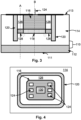
- Figure 4 shows a top view of the semiconductor device in Figure 3 according to an embodiment of the present disclosure.
- an active component 130 is positioned within the first well region 116. Although the active component 130 is shown as positioned centrally within the first well region 116 in Figure 4 , it will be appreciated that this is not limiting.
- the active component 130 may, for example, be a transistor or a diode, although any type of active component may be provided.
- a plurality of electrical contacts 124 are provided on the top surface of the substrate in electrical contact with the first well region 116.
- the electrical contacts 124 control the potential of the first buried layer 118.
- the second well region 126 surrounds (or is perimetric to) the first well region 116.
- the isolation trench 120 surrounds (or is perimetric to) the second well region 126.
- the at least one epitaxial layer 114 surrounds the isolation trench 120. In some embodiments, the at least one epitaxial layer 114 may be replaced by a single substrate 110.
- the first buried layer 118 is not visible as this is provided underneath the first well region.
- the second buried layer 128 is not visible as this is provided underneath the second well region 126.
- Figure 4 is a schematic representation of a plan view of the semiconductor device, and the respective layers may have different shapes and relative sizes to those shown.
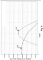
- Figure 5 is a graph showing how doping concentration may vary with depth in the semiconductor along line A in Figure 3 . Accordingly, the y axis is doping concentration per cm 3 , and the x axis is depth from the top surface of the substrate.
- Line 126 in Figure 5 represents the second well region 126, which in this embodiment comprises a single doping species.
- the doping species is phosphorous, although other elements may be used.
- the peak doping concentration for the second well region is off the order of 1 ⁇ 10 16 /cm 3 .
- Line 128 in Figure 5 represents the second buried layer 128.
- the second buried layer 128 is positioned below (at a lower depth to) the second well region 116.
- the second buried layer 128 comprises phosphorous, although other doping elements may be used.
- the peak doping concentration for the second buried layer 128 is between 1 ⁇ 10 16 /cm 3 and 1 ⁇ 10 17 /cm 3 .
- the peak doping concentration for the second buried layer 128 in this embodiment is close to 1 ⁇ 10 17 /cm 3 .
- Figure 6 shows how doping concentration may vary with depth in the semiconductor along line B in Figure 3 .
- the y axis is doping concentration per cm 3
- the x axis is depth from the top surface of the substrate.
- the x axis may be from 0 ⁇ m to 10 ⁇ m in both Figure 5 and 6 , but it will be appreciated that this scale is not limiting and may vary depending on the particular application.
- Line 116 in Figure 6 represents the first well region 116, which in this embodiment comprises a single doping species, wherein the single doping species is phosphorous, although other elements may be used.
- the peak doping concentration for the first well region is between 1 ⁇ 10 17 /cm 3 and 1 ⁇ 10 18 /cm 3 (for example, around 5 ⁇ 10 17 /cm 3 ). Accordingly, a comparison of Figures 5 and 6 shows that the first well region 116 has a higher peak doping concentration than the second well region 126.
- the first buried layer 118 is comprises two doping species, which are represented by lines 118-1 and 118-2.
- line 118-1 represents the buried layer doped with antimony
- line 118-2 represents the buried layer doped with phosphorous.
- different doping elements may be used and optionally only a single doping species may be used.
- the antimony doped buried layer 118-1 has a peak doping concentration of the order of 1 ⁇ 10 19 /cm 3 , as shown in Figure 6 .
- the phosphorous doped buried layer 118-2 has a lower peak doping concentration of the order of 1 ⁇ 10 16 /cm 3 .
- a comparison of Figures 5 and 6 shows that the peak doping concentration of the second buried layer 128 is configured to be at a slightly lower depth in the substrate than the peak doping concentration of the antimony doped buried layer 118-1. This is to mitigate the lateral electric field strength at the edge of first buried layer, which has been found to improve the stability of the breakdown voltage.
- Figure 7 is a flowchart illustrating a method of manufacturing a semiconductor device according to an embodiment of the present disclosure.
- the method comprises providing a substrate 110.
- the substrate 110 may have a single layer, or multiple layers.
- the substrate 110 may have a first conductivity type, such as but not limited to p-type or positive type conductivity.
- the method comprises providing a first buried layer 118 at a first depth within the substrate 110.
- the first buried layer 118 may have a second conductivity type, such as but not limited to n-type or negative type conductivity.
- the first buried layer 118 has a first doping concentration.
- the method comprises providing a second buried layer 128 at the first depth within the substrate 110.
- the second buried layer 128 may have the second conductivity type, same as the first buried layer 118.
- the second buried layer 128 has a second doping concentration which is less than the first doping concentration of the first buried layer 118.
- the first doping concentration may be of the order of 1000 times higher than the second doping concentration.
- steps 202 and 204 may be combined in a single step.
- the substrate 110 may be provided as a base substrate with an epitaxial layer on top.
- the first and second buried layers 118, 128 may be implanted in the epitaxial layer.
- steps 204 and 206 there may be an intermediate step (not shown) of growing a second epitaxial layer on top of the first epitaxial layer and the first and second buried layers 118, 128.
- the method comprises providing a first well region 116 between the first buried layer 118 and a top surface of the substrate 110 (e.g., the top surface of the second epitaxial layer).
- the first well region 116 is stacked on top of the first buried layer 118 when viewed from above the substrate.
- a second well region 126 is provided perimetric to (or surrounding) the first well region.
- the second well region 126 may be stacked on top of the second buried layer, such that it is positioned between the second buried layer 128 and the top surface of the substrate.
- the first and second well regions may have the second conductivity type, the same as the first and second buried layers.
- the doping concentration of both the first and second well regions may be less than the first doping concentration of the first buried layer.
- steps 206 and 208 may be combined in a single step.
- an isolation trench 120 is inserted into the substrate.
- the isolation trench 120 surrounds, or is perimetric to, the second well region 126 and the second buried layer 128.
- the isolation trench 120 extends to a depth within the substate that exceeds the depth of the first and second buried layers 118, 128.
- the trench 120 may be filled, or partially filled, with a polysilicon material.
- steps 200 to 210 could be carried out in a different order to the order shown in Figure 7 .
- a semiconductor device comprising a substrate having a first conductivity type, the substrate having a top surface and a bottom surface, a first buried layer disposed in the substrate at a first depth from the top surface, wherein the first buried layer has a second conductivity type and a first doping concentration, a second buried layer adjacent and surrounding the first buried layer at the first depth, wherein the second buried layer has the second conductivity type and a second doping concentration, wherein the second doping concentration is less than the first doping concentration, and an isolation trench disposed in the substrate and surrounding the second buried layer, wherein the isolation trench extends from the top surface of the substrate to a second depth, the second depth exceeding the first depth.
- a method of manufacture is also provided, as described above.
Landscapes
- Element Separation (AREA)
Abstract
Description
- The present specification relates to isolation structures for an active component in a semiconductor device. In particular, the present specification relates to trench isolation.
- Bipolar CMOS DMOS (BCD) process technology enables incorporation of analog components, digital components and high voltage (HV) devices into a single chip or integrated circuit (IC). These components are designed such that they do not interfere with (for example, latch up with) adjacent components on a substrate. Hence, there is a need to properly isolate adjacent components from each other. A variety of different isolation schemes exist such as junction-based isolation or trench-based isolation in a bulk wafer or trench-based isolation in a SOI (Silicon -on-insulator) wafer.
- A typical design of a trench-based isolation involves a heavily doped buried layer (BL) that intersects a trench oxide where the trench is partially or fully filled with oxide.
- Aspects of the present disclosure are set out in the accompanying independent and dependent claims. Combinations of features from the dependent claims may be combined with features of the independent claims as appropriate and not merely as explicitly set out in the claims.
- According to a first aspect of the present disclosure, there is provided a semiconductor device comprising a substrate having a first conductivity type, the substrate having a top surface and a bottom surface. A first buried layer is disposed in the substrate at a first depth from the top surface, wherein the first buried layer has a second conductivity type and a first doping concentration. A second buried layer is adjacent to and surrounds the first buried layer at the first depth, wherein the second buried layer has the second conductivity type and a second doping concentration, wherein the second doping concentration is less than the first doping concentration. An isolation trench is disposed in the substrate and surrounds the second buried layer, wherein the isolation trench extends from the top surface of the substrate to a second depth, the second depth exceeding the first depth.
- It will be appreciated that the second conductivity type is different to the first conductivity type.
- The second buried layer is perimetric to the first buried layer. The isolation trench is perimetric to the second buried layer.
- Optionally, the first doping concentration may be of the order of 1018/cm3 or 1019/cm3. Optionally, the first doping concentration may be between 5×10¹⁸/cm3 and 5×10¹⁹/cm3.
- In some embodiments the first buried layer may comprise at least two doping species.
- Optionally, the second doping concentration is of the order of 1016/cm3 or 1017/cm3. Optionally, the second doping concentration may be between 5×10¹⁶/cm3 and 5×10¹⁷/cm3.
- It will be appreciated that the doping concentrations referred to in the present disclosure may be the peak doping concentration for the respective semiconductor layer.
- Optionally, the substrate comprises a base substrate and at least one epitaxial layer disposed over the base substrate. The at least one epitaxial layer may have the first conductivity type. The isolation trench and the first and second buried layers may be disposed in the at least one epitaxial layer. Thus, the top surface of the substrate may be the top surface of the at least one epitaxial layer. The bottom surface of the substrate may be a bottom surface of the base substrate. It will be appreciated that various multi-layer substrates could be used.
- In some embodiments, the semiconductor device further comprises a first well region disposed between the top surface of the substrate and the first buried layer. The first well region may have the second conductivity type. The first well region may be bounded by the isolation trench.
- In some embodiments, the semiconductor device further comprises an active component provided in the first well region. Optionally, the active component may be a transistor, or a diode, but is not limited to these examples.
- Optionally, a second well region may be disposed between the first well region and the isolation trench. The second well region may have the second conductivity type and may surround the first well region.
- The second well region may be perimetric to the first well region. The isolation trench may be perimetric to the second well region.
- Optionally, the second well region may have a doping concentration that is the same as, or of the same order as, the second doping concentration.
- In some embodiments, the second well region may have a doping concentration that is of the order of 1016/cm3.
- In some embodiments, the first well region may have a doping concentration that is of the order of 1017/cm3 or 1018/cm3. Optionally, the first well region may have a doping concentration that is between the first doping concentration and the second doping concentration.
- Optionally, a width of the second buried layer is less than a width of the first buried layer. The width of the second buried layer is the distance between the isolation trench and the first buried layer.
- Optionally, a width of the second buried layer between the isolation trench and the first buried layer is at least 1 µm. Optionally, a width of the second buried layer between the isolation trench and the first buried layer is between 1 and 5 µm.
- Optionally, the isolation trench contains a polysilicon material.
- Optionally, the first and second buried layers have the same height.
- Optionally, the second buried layer is configured such that a breakdown region is spaced from the isolation trench. The breakdown region is defined as a region or location which is susceptible to electrical breakdown due to a high electric field strength. This may also be referred to as an electrical hotspot.
- Optionally, the second buried layer is configured such that the breakdown region is located proximate a junction between the first buried layer and the second buried layer. Optionally, the second buried layer is configured such that the breakdown region is located proximate an edge of the first buried layer.
- Thus, the breakdown region may be spaced from the trench by a distance equal to the width of the second buried layer.
- According to a second aspect of the present disclosure, there is provided a method of manufacturing a semiconductor device, comprising providing a substrate having a first conductivity type, the substrate having a top surface and a bottom surface, providing a first buried layer in the substrate at a first depth from the top surface, wherein the first buried layer has a second conductivity type and a first doping concentration, providing a second buried layer adjacent and surrounding the first buried layer at the first depth, wherein the second buried layer has the second conductivity type and a second doping concentration, wherein the second doping concentration is less than the first doping concentration, and providing an isolation trench in the substrate surrounding the second buried layer, wherein the isolation trench extends from the top surface of the substrate to a second depth, the second depth exceeding the first depth.
- It will be appreciated that the method may comprise method steps for manufacturing a semiconductor device according to any embodiment or example of the first aspect of the disclosure.
- Optionally, the first and second buried layers may be inserted or implanted in a single step.
- Optionally, the method may include providing a first well region between the top surface of the substrate and the first buried layer. The first well region may have the second conductivity type.
- Optionally, the method may include providing a second well region between the isolation trench and the first well region, such that the second well region surrounds or is perimetric to the first well region. The second well region may have the second conductivity type. The second well region may have a lower doping concentration than the first well region.
- Optionally, the first and second well regions may be inserted or implanted in a single step. Optionally, the first and second well regions may be inserted or implanted before the isolation trench is provided.
- The method may include providing a polysilicon material in the isolation trench.
- The method may comprise providing a base substrate, the base substrate having the first conductivity type. The method may comprise providing a first epitaxial layer over the base substrate, the first epitaxial layer having the first conductivity type.
- The method may include implanting the first and second buried layers into the first epitaxial layer. A second epitaxial layer may be grown over the first epitaxial layer and the first and second buried layers.
- Illustrative embodiments of this disclosure will be described hereinafter, by way of example only, with reference to the accompanying drawings in which like reference signs relate to like elements and in which:
-
Figure 1 - shows a cross-sectional view of a prior art semiconductor device; -
Figure 2 - shows a cross-sectional view of another prior art semiconductor device; -
Figure 3 - shows a cross-sectional view of a semiconductor device according to an embodiment of the present disclosure; -
Figure 4 - shows a top view of a semiconductor device according to an embodiment of the present disclosure; -
Figure 5 - is a graph showing how, in one embodiment of the present disclosure, doping concentration varies with depth along line A inFigure 3 ; -
Figure 6 - is a graph showing how, in one embodiment of the present disclosure, doping concentration varies with depth along line B inFigure 3 ; and -
Figure 7 - is flowchart of a method of manufacture according to an embodiment of the present disclosure. - Embodiments of this disclosure are described in the following with reference to the accompanying drawings. It will be appreciated that the drawings are schematic illustrations and are not drawn to scale.
-
Figure 1 is a cross-sectional view of a prior art semiconductor device. The semiconductor device comprises asubstrate 10 formed of abase substrate 12 and at least oneepitaxial layer 14 formed on top of thebase substrate 12. Thesubstrate 10 has abottom surface 11 and atop surface 13. It will be appreciated that in some embodiments thesubstrate 10 may be a single layer, or the substrate may have a plurality of different layers. - A heavily doped buried
layer 18 is disposed in thesubstrate 10 at a depth from thetop surface 13 of the substrate. The buriedlayer 18 is surrounded by anisolation trench 20. Thetrench 20 is usually filled with an oxide material. Awell region 16 is disposed between thetop surface 13 and the buriedlayer 18. Thewell region 16 is bounded by (or surrounded by) thetrench 20. At least oneelectrical contact 24 is electrically connected to thewell region 16 and the buriedlayer 18. The electrical contact(s) 24 control the potential of the buriedlayer 18. - In use (but not shown in
Figure 1 ) an active component is disposed in thewell region 16. Theisolation trench 20 and buriedlayer 18 are provided to attempt to electrically isolate the active component from neighbouring components on thesubstrate 10, such that adjacent active components do not interfere with each other. Thetrench 20 provides a physical barrier, due to the oxide filling, and the buriedlayer 18, provides an electrical barrier. - However, it has been found that the semiconductor device shown in
Figure 1 is susceptible to breakdown voltage shift over time. Avalanche breakdown occurs when an electric field generated by a voltage in a semiconducting region exceeds a critical value, such that the object becomes a conductor. This is because the electric field becomes strong enough generate a lot of electron/hole pairs that create a lot of current quickly. The breakdown voltage of an object is the voltage at which this breakdown occurs. The breakdown voltage depends on a variety of factors including the composition and shape of the object. - Accordingly, electrical breakdown usually initiates at the region that has the highest electric field. In this disclosure this region is called the breakdown region, or hotspot region, and is represented by a star in
Figures 1 to 3 . - If there is a shift in the breakdown voltage over time, this means that the voltage at which electrical breakdown occurs is not stable and changes over time. If the breakdown voltage shifts to lower voltages over time, then this can result in the isolation structure failing when the semiconductor device is subjected to high voltages.
- It has been found that the breakdown voltage of the prior art in
Figure 1 shifts to lower voltages over time. This is because the breakdown region (i.e., the high electric field region at which breakdown occurs) is located proximate to thetrench 20, as shown by the stars. This causes the breakdown voltage to change over time due to hot electron or hot hole injection towards the trench oxide causing Ox-Si interface charging, or possibly due to hot electron or hot hole injection landing in the conductive polysilicon region of the trench. - Another prior art example is shown in
Figure 2 . Features which are common betweenfigures 1 and 2 have been given the same reference numeral. InFigure 2 , there is asecond isolation trench 22 provided, which is spaced from and surrounds thefirst isolation trench 20. Bothtrenches layer 18 and at least a portion of thewell region 16. Thetrenches first trench 20, as shown by the stars inFigure 2 . Again, it has been found that the semiconductor device shown inFigure 2 is susceptible to breakdown voltage (BV) shift over time. As stated above, this BV shift can be caused due to hot electron or hot hole injection towards the trench oxide causing Ox-Si interface charging, or possibly due to hot electron or hot hole injection landing in the conductive polysilicon region of the trench. - A cross-sectional view of a semiconductor device according to an embodiment of the present invention is shown in
Figure 3 . - The semiconductor device comprises a
substrate 110 formed of abase substrate 112 and at least oneepitaxial layer 114 formed on top of thebase substrate 112. Thesubstrate 110 has abottom surface 111 and atop surface 113. It will be appreciated that in some embodiments thesubstrate 110 may be a single layer, or the substrate may have a plurality of different layers. Thesubstrate 110 has a first conductivity type, for example positive or p conductivity. - A first buried
layer 118 is disposed in thesubstrate 110 at a depth from thetop surface 113 of the substrate. The first buriedlayer 118 has a second conductivity type, which is different to the conductivity type of thesubstrate 110. The first buriedlayer 118 is doped at a first doping concentration. - A second buried
layer 128 is disposed in thesubstate 110 at the same depth as the first buriedlayer 118. The second buriedlayer 128 is adjacent to and surrounds the first buriedlayer 118. Thus, the second buriedlayer 128 is perimetric to the first buriedlayer 118. - The second buried
layer 128 has a second conductivity type (opposite to thesubstrate 110 and the same as the first buried layer 118). The second buriedlayer 128 is doped at a second doping concentration. The second doping concentration is less than the first doping concentration. Thus, the second buriedlayer 128 can be referred to as a light buried layer. - An
isolation trench 120 is provided that extends to a depth that exceeds the first depth of the first and second buriedlayers isolation trench 120 may extend from thetop surface 113 of the substrate to thebase substate 112, or to the bottom surface of thesubstrate 111. Thetrench 120 comprises a polysilicon material. Theisolation trench 120 enclosed or is perimetric to the second buriedlayer 128. - A
first well region 116 is disposed between thetop surface 113 and the buriedlayer 118. Thefirst well region 116 has the second conductivity type, the same as the first and second buried layers. At least oneelectrical contact 124 is electrically connected to thefirst well region 116. - A
second well region 126 is provided between theisolation trench 120 and thefirst well region 116. Thesecond well region 126 is therefore perimetric to the first well region, as it surrounds the perimeter of thefirst well region 116. Theisolation trench 120 is perimetric to thesecond well region 126. - The
second well region 126 has the second conductivity type and a doping concentration that is less than the doping concentration of thefirst well region 116. In some embodiments, thesecond well region 126 may have a doping concentration that is the same as, or of the same order as, the second buriedlayer 128. - In use (see
Figure 4 ) an active component is disposed in thefirst well region 116. The combination of thefirst well region 116, first buriedlayer 118 and the active component can be referred to as a high voltage (HV) tub. The structure shown inFigure 3 is configured to electrically isolate the active component from neighbouring components on thesubstrate 110. Optionally, thesubstrate 110 may comprise a plurality of structures as shown inFigure 3 (i.e., a plurality ofisolation trenches 120, first and second buriedlayers well regions 116, 126), wherein eachfirst well region 116 is configured to contain a respective active component. For simplicity, only a single isolation structure has been shown inFigure 3 . - The second buried
layer 128 acts as a spacer between the first buriedlayer 118 and theisolation trench 120. In practice, this changes the location of the breakdown region, which is represented by stars inFigure 3 . As shown, the provision of the second buriedlayer 128 having a doping concentration that is less than the doping concentration of the first buriedlayer 118 spaces or translates the breakdown region away from theisolation trench 120 by a distance equal to the width of the second buriedlayer 128. In some embodiments, the second buriedlayer 128 may have a width of at least 1 µm. The second buriedlayer 128 may have a width equal to between 1 and 5 µm. - By moving the breakdown region away from the
isolation trench 120 this reduces, or eliminates, breakdown voltage shift over time, even if the semiconductor device is exposed to high voltage and/or high temperatures for a prolonged period of time. In one particular embodiment, the breakdown voltage of the semiconductor device was tested, and the semiconductor device was then constantly stressed at 80V and 150°C for around 1 week. The breakdown voltage was then retested and was found to be only 0.5 V different to the initial breakdown voltage. Thus, in the semiconductor device shown inFigure 3 , the breakdown voltage remains more stable or constant over time compared to the prior art devices. -
Figure 4 shows a top view of the semiconductor device inFigure 3 according to an embodiment of the present disclosure. - As shown, an
active component 130 is positioned within thefirst well region 116. Although theactive component 130 is shown as positioned centrally within thefirst well region 116 inFigure 4 , it will be appreciated that this is not limiting. Theactive component 130 may, for example, be a transistor or a diode, although any type of active component may be provided. - A plurality of
electrical contacts 124 are provided on the top surface of the substrate in electrical contact with thefirst well region 116. Theelectrical contacts 124 control the potential of the first buriedlayer 118. - The
second well region 126 surrounds (or is perimetric to) thefirst well region 116. Theisolation trench 120 surrounds (or is perimetric to) thesecond well region 126. The at least oneepitaxial layer 114 surrounds theisolation trench 120. In some embodiments, the at least oneepitaxial layer 114 may be replaced by asingle substrate 110. InFigure 4 , the first buriedlayer 118 is not visible as this is provided underneath the first well region. Similarly, the second buriedlayer 128 is not visible as this is provided underneath thesecond well region 126. - It will be appreciated that
Figure 4 is a schematic representation of a plan view of the semiconductor device, and the respective layers may have different shapes and relative sizes to those shown. -
Figure 5 is a graph showing how doping concentration may vary with depth in the semiconductor along line A inFigure 3 . Accordingly, the y axis is doping concentration per cm3, and the x axis is depth from the top surface of the substrate. -
Line 126 inFigure 5 represents thesecond well region 126, which in this embodiment comprises a single doping species. In this embodiment the doping species is phosphorous, although other elements may be used. As thesecond well region 126 is the closest to the top surface of the substrate, this layer has the highest doping concentration towards x=0 along the cross-sectional line A (seeFigure 3 ). In this embodiment the peak doping concentration for the second well region is off the order of 1 ×10¹⁶ /cm3. -
Line 128 inFigure 5 represents the second buriedlayer 128. As is shown inFigure 3 , along cross-sectional line A the second buriedlayer 128 is positioned below (at a lower depth to) thesecond well region 116. In this embodiment, the second buriedlayer 128 comprises phosphorous, although other doping elements may be used. The peak doping concentration for the second buriedlayer 128 is between 1 ×10¹⁶ /cm3 and 1 ×10¹⁷ /cm3. As shown inFigure 5 , the peak doping concentration for the second buriedlayer 128 in this embodiment is close to 1 ×10¹⁷ /cm3. -
Figure 6 shows how doping concentration may vary with depth in the semiconductor along line B inFigure 3 . Accordingly, the y axis is doping concentration per cm3, and the x axis is depth from the top surface of the substrate. Optionally, the x axis may be from 0 µm to 10 µm in bothFigure 5 and6 , but it will be appreciated that this scale is not limiting and may vary depending on the particular application. -
Line 116 inFigure 6 represents thefirst well region 116, which in this embodiment comprises a single doping species, wherein the single doping species is phosphorous, although other elements may be used. As thefirst well region 116 is the closest to the top surface of the substrate, this layer has the highest doping concentration towards x=0 along the cross-sectional line B (seeFigure 3 ). In this embodiment the peak doping concentration for the first well region is between 1 ×10¹⁷ /cm3 and 1 ×10¹⁸ /cm3 (for example, around 5 ×10¹⁷ /cm3). Accordingly, a comparison ofFigures 5 and6 shows that thefirst well region 116 has a higher peak doping concentration than thesecond well region 126. - In this embodiment, the first buried
layer 118 is comprises two doping species, which are represented by lines 118-1 and 118-2. In this embodiment, line 118-1 represents the buried layer doped with antimony, and line 118-2 represents the buried layer doped with phosphorous. In other embodiments, different doping elements may be used and optionally only a single doping species may be used. - The antimony doped buried layer 118-1 has a peak doping concentration of the order of 1 ×10¹⁹ /cm3, as shown in
Figure 6 . The phosphorous doped buried layer 118-2 has a lower peak doping concentration of the order of 1 ×10¹⁶ /cm3. - A comparison of
Figures 5 and6 shows that the peak doping concentration of the second buriedlayer 128 is configured to be at a slightly lower depth in the substrate than the peak doping concentration of the antimony doped buried layer 118-1. This is to mitigate the lateral electric field strength at the edge of first buried layer, which has been found to improve the stability of the breakdown voltage. - It will be appreciated that the various semiconductor layers are not limited to the doping elements or concentrations described above or shown in
Figure 5 or6 . -
Figure 7 is a flowchart illustrating a method of manufacturing a semiconductor device according to an embodiment of the present disclosure. - In
step 200 the method comprises providing asubstrate 110. Thesubstrate 110 may have a single layer, or multiple layers. Thesubstrate 110 may have a first conductivity type, such as but not limited to p-type or positive type conductivity. - In
step 202 the method comprises providing a first buriedlayer 118 at a first depth within thesubstrate 110. The first buriedlayer 118 may have a second conductivity type, such as but not limited to n-type or negative type conductivity. The first buriedlayer 118 has a first doping concentration. - In
step 204 the method comprises providing a second buriedlayer 128 at the first depth within thesubstrate 110. The second buriedlayer 128 may have the second conductivity type, same as the first buriedlayer 118. The second buriedlayer 128 has a second doping concentration which is less than the first doping concentration of the first buriedlayer 118. In some embodiments, the first doping concentration may be of the order of 1000 times higher than the second doping concentration. - It will be appreciated that
steps - Optionally, the
substrate 110 may be provided as a base substrate with an epitaxial layer on top. The first and second buriedlayers steps layers - In
step 206 the method comprises providing afirst well region 116 between the first buriedlayer 118 and a top surface of the substrate 110 (e.g., the top surface of the second epitaxial layer). Thus, thefirst well region 116 is stacked on top of the first buriedlayer 118 when viewed from above the substrate. - In step 208 a
second well region 126 is provided perimetric to (or surrounding) the first well region. Thesecond well region 126 may be stacked on top of the second buried layer, such that it is positioned between the second buriedlayer 128 and the top surface of the substrate. - The first and second well regions may have the second conductivity type, the same as the first and second buried layers. The doping concentration of both the first and second well regions may be less than the first doping concentration of the first buried layer.
- It will be appreciated that
steps - At
step 210 anisolation trench 120 is inserted into the substrate. Theisolation trench 120 surrounds, or is perimetric to, thesecond well region 126 and the second buriedlayer 128. Theisolation trench 120 extends to a depth within the substate that exceeds the depth of the first and second buriedlayers trench 120 may be filled, or partially filled, with a polysilicon material. - It will be appreciated that
steps 200 to 210 could be carried out in a different order to the order shown inFigure 7 . - Accordingly, there has been described a semiconductor device comprising a substrate having a first conductivity type, the substrate having a top surface and a bottom surface, a first buried layer disposed in the substrate at a first depth from the top surface, wherein the first buried layer has a second conductivity type and a first doping concentration, a second buried layer adjacent and surrounding the first buried layer at the first depth, wherein the second buried layer has the second conductivity type and a second doping concentration, wherein the second doping concentration is less than the first doping concentration, and an isolation trench disposed in the substrate and surrounding the second buried layer, wherein the isolation trench extends from the top surface of the substrate to a second depth, the second depth exceeding the first depth. A method of manufacture is also provided, as described above.
- Although particular embodiments of this disclosure have been described, it will be appreciated that many modifications/additions and/or substitutions may be made within the scope of the claims.
Claims (15)
- A semiconductor device comprising:a substrate having a first conductivity type, the substrate having a top surface and a bottom surface;a first buried layer disposed in the substrate at a first depth from the top surface, wherein the first buried layer has a second conductivity type and a first doping concentration;a second buried layer adjacent and surrounding the first buried layer at the first depth, wherein the second buried layer has the second conductivity type and a second doping concentration, wherein the second doping concentration is less than the first doping concentration; andan isolation trench disposed in the substrate and surrounding the second buried layer, wherein the isolation trench extends from the top surface of the substrate to a second depth, the second depth exceeding the first depth.
- The semiconductor device of claim 1, wherein the first doping concentration is between 5×10¹⁸/CM3 and 5×10¹⁹/cm3.
- The semiconductor device of claim 1 or claim 2, wherein the second doping concentration is between 5×10¹⁶/cm3 and 5×10¹⁷/cm3.
- The semiconductor device of any preceding claim, wherein the substrate comprises a base substrate and at least one epitaxial layer disposed over the base substrate, wherein the isolation trench and the first and second buried layers are disposed in the at least one epitaxial layer.
- The semiconductor device of any preceding claim, further comprising a first well region disposed between the top surface of the substrate and the first buried layer, wherein the first well region has the second conductivity type.
- The semiconductor device of claim 5, further comprising an active component provided in the first well region.
- The semiconductor device of claim 5 or claim 6, further comprising a second well region disposed between the first well region and the isolation trench, wherein the second well region has the second conductivity type and surrounds the first well region.
- The semiconductor device of claim 7, wherein the second well region has a doping concentration that is of the same order as the second doping concentration.
- The semiconductor device of any preceding claim, wherein a width of the second buried layer between the isolation trench and the first buried layer is less than a width of the first buried layer.
- The semiconductor device of any preceding claim, wherein a width of the second buried layer between the isolation trench and the first buried layer is between 1 and 5 µm.
- The semiconductor device of any preceding claim, wherein the isolation trench contains a polysilicon material.
- The semiconductor device of any preceding claim, wherein the first and second buried layers have the same height.
- The semiconductor device of any preceding claim, wherein the second buried layer is configured such that a breakdown region is spaced from the isolation trench.
- The semiconductor device of claim 13, wherein:the second buried layer is configured such that the breakdown region is located proximate a junction between the first buried layer and the second buried layer; orthe breakdown region is spaced from the isolation trench by a distance equal to the width of the second buried layer.
- A method of manufacturing a semiconductor device, comprising:providing a substrate having a first conductivity type, the substrate having a top surface and a bottom surface;providing a first buried layer in the substrate at a first depth from the top surface, wherein the first buried layer has a second conductivity type and a first doping concentration;providing a second buried layer adjacent and surrounding the first buried layer at the first depth, wherein the second buried layer has the second conductivity type and a second doping concentration, wherein the second doping concentration is less than the first doping concentration; andproviding an isolation trench in the substrate surrounding the second buried layer, wherein the isolation trench extends from the top surface of the substrate to a second depth, the second depth exceeding the first depth.
Priority Applications (3)
| Application Number | Priority Date | Filing Date | Title |
|---|---|---|---|
| EP22201462.3A EP4354496B1 (en) | 2022-10-13 | 2022-10-13 | Isolation structure for an active component |
| US18/473,950 US20240128316A1 (en) | 2022-10-13 | 2023-09-25 | Isolation structure for an active component |
| CN202311326560.1A CN117894742A (en) | 2022-10-13 | 2023-10-13 | Isolation structures for active components |
Applications Claiming Priority (1)
| Application Number | Priority Date | Filing Date | Title |
|---|---|---|---|
| EP22201462.3A EP4354496B1 (en) | 2022-10-13 | 2022-10-13 | Isolation structure for an active component |
Publications (2)
| Publication Number | Publication Date |
|---|---|
| EP4354496A1 true EP4354496A1 (en) | 2024-04-17 |
| EP4354496B1 EP4354496B1 (en) | 2025-05-14 |
Family
ID=83996878
Family Applications (1)
| Application Number | Title | Priority Date | Filing Date |
|---|---|---|---|
| EP22201462.3A Active EP4354496B1 (en) | 2022-10-13 | 2022-10-13 | Isolation structure for an active component |
Country Status (3)
| Country | Link |
|---|---|
| US (1) | US20240128316A1 (en) |
| EP (1) | EP4354496B1 (en) |
| CN (1) | CN117894742A (en) |
Citations (4)
| Publication number | Priority date | Publication date | Assignee | Title |
|---|---|---|---|---|
| US20070063274A1 (en) * | 2005-02-24 | 2007-03-22 | Ryo Kanda | Semiconductor device |
| CN104362095A (en) * | 2014-11-05 | 2015-02-18 | 北京大学 | Production method of tunneling field-effect transistor |
| EP3553822A1 (en) * | 2018-04-09 | 2019-10-16 | NXP USA, Inc. | Esd protection device, semiconductor device that includes an esd protection device, and method of manufacturing same |
| US20220190116A1 (en) * | 2020-12-11 | 2022-06-16 | Globalfoundries U.S. Inc. | Integrated circuit (ic) structure with body contact to well with multiple diode junctions |
Family Cites Families (10)
| Publication number | Priority date | Publication date | Assignee | Title |
|---|---|---|---|---|
| US8921202B2 (en) * | 2011-01-07 | 2014-12-30 | Vanguard International Semiconductor Corporation | Semiconductor device and fabrication method thereof |
| US9793153B2 (en) * | 2011-09-20 | 2017-10-17 | Alpha And Omega Semiconductor Incorporated | Low cost and mask reduction method for high voltage devices |
| US9214457B2 (en) * | 2011-09-20 | 2015-12-15 | Alpha & Omega Semiconductor Incorporated | Method of integrating high voltage devices |
| EP2996153B1 (en) * | 2014-09-12 | 2019-05-22 | Nxp B.V. | Bipolar transistor and method of manufacturing the same |
| US9306060B1 (en) * | 2014-11-20 | 2016-04-05 | Freescale Semiconductor Inc. | Semiconductor devices and related fabrication methods |
| KR20170059706A (en) * | 2015-11-23 | 2017-05-31 | 페어차일드코리아반도체 주식회사 | Power semiconductor devices |
| US10211199B2 (en) * | 2017-03-31 | 2019-02-19 | Alpha And Omega Semiconductor (Cayman) Ltd. | High surge transient voltage suppressor |
| US20200194581A1 (en) * | 2018-12-18 | 2020-06-18 | Vanguard International Semiconductor Corporation | Semiconductor device and method for forming the same |
| KR102233049B1 (en) * | 2019-07-24 | 2021-03-26 | 주식회사 키 파운드리 | Semiconductor Device with Controllable Channel Length and Manufacturing Method thereof |
| US12532537B2 (en) * | 2022-08-03 | 2026-01-20 | Vanguard International Semiconductor Corporation | Semiconductor device with a deep trench isolation structure and buried layers for reducing substrate leakage current and avoiding latch-up effect, and fabrication method thereof |
-
2022
- 2022-10-13 EP EP22201462.3A patent/EP4354496B1/en active Active
-
2023
- 2023-09-25 US US18/473,950 patent/US20240128316A1/en active Pending
- 2023-10-13 CN CN202311326560.1A patent/CN117894742A/en active Pending
Patent Citations (4)
| Publication number | Priority date | Publication date | Assignee | Title |
|---|---|---|---|---|
| US20070063274A1 (en) * | 2005-02-24 | 2007-03-22 | Ryo Kanda | Semiconductor device |
| CN104362095A (en) * | 2014-11-05 | 2015-02-18 | 北京大学 | Production method of tunneling field-effect transistor |
| EP3553822A1 (en) * | 2018-04-09 | 2019-10-16 | NXP USA, Inc. | Esd protection device, semiconductor device that includes an esd protection device, and method of manufacturing same |
| US20220190116A1 (en) * | 2020-12-11 | 2022-06-16 | Globalfoundries U.S. Inc. | Integrated circuit (ic) structure with body contact to well with multiple diode junctions |
Also Published As
| Publication number | Publication date |
|---|---|
| EP4354496B1 (en) | 2025-05-14 |
| US20240128316A1 (en) | 2024-04-18 |
| CN117894742A (en) | 2024-04-16 |
Similar Documents
| Publication | Publication Date | Title |
|---|---|---|
| US10886160B2 (en) | Sinker to buried layer connection region for narrow deep trenches | |
| US7723800B2 (en) | Deep trench isolation for power semiconductors | |
| US10373944B2 (en) | ESD protection circuit with integral deep trench trigger diodes | |
| US7855427B2 (en) | Semiconductor device with a plurality of isolated conductive films | |
| US20050181577A1 (en) | Method of manufacturing a superjunction device | |
| US10672758B2 (en) | Electrostatic discharge protection structure, method for manufacturing an electrostatic discharge protection structure, and vertical thyristor structure | |
| US20130087852A1 (en) | Edge termination structure for power semiconductor devices | |
| JP2019521529A (en) | POWER DEVICE AND METHOD FOR MANUFACTURING THE SAME | |
| EP1756949A2 (en) | Semiconductor device and method of forming the same | |
| KR100780967B1 (en) | Schottky Diode Structures for High Voltage | |
| US12125923B2 (en) | High voltage diode on SOI substrate with trench-modified current path | |
| US9425266B2 (en) | Integrated floating diode structure and method therefor | |
| US11652167B2 (en) | Semiconductor device having junction termination structure and method of formation | |
| US20130320485A1 (en) | Semiconductor device | |
| JP2005531141A (en) | Semiconductor device having end structure | |
| US11049853B2 (en) | ESD protection device with breakdown voltage stabilization | |
| JP2014086723A (en) | High voltage diode | |
| KR20090071805A (en) | Schottky Diodes in Semiconductor Devices and Manufacturing Method Thereof | |
| EP4354496B1 (en) | Isolation structure for an active component | |
| US10354926B2 (en) | Integrated circuit with improved resistive region | |
| CN118866809A (en) | Deep trench isolation structure and manufacturing method thereof | |
| US6696707B2 (en) | High voltage integrated switching devices on a bonded and trenched silicon substrate | |
| US11486944B2 (en) | Isolated hall sensor structure | |
| US20100187650A1 (en) | Insulated well with a low stray capacitance for electronic components | |
| US20240204114A1 (en) | Variable-capacitance diode |
Legal Events
| Date | Code | Title | Description |
|---|---|---|---|
| PUAI | Public reference made under article 153(3) epc to a published international application that has entered the european phase |
Free format text: ORIGINAL CODE: 0009012 |
|
| STAA | Information on the status of an ep patent application or granted ep patent |
Free format text: STATUS: THE APPLICATION HAS BEEN PUBLISHED |
|
| AK | Designated contracting states |
Kind code of ref document: A1 Designated state(s): AL AT BE BG CH CY CZ DE DK EE ES FI FR GB GR HR HU IE IS IT LI LT LU LV MC ME MK MT NL NO PL PT RO RS SE SI SK SM TR |
|
| STAA | Information on the status of an ep patent application or granted ep patent |
Free format text: STATUS: REQUEST FOR EXAMINATION WAS MADE |
|
| 17P | Request for examination filed |
Effective date: 20241017 |
|
| RBV | Designated contracting states (corrected) |
Designated state(s): AL AT BE BG CH CY CZ DE DK EE ES FI FR GB GR HR HU IE IS IT LI LT LU LV MC ME MK MT NL NO PL PT RO RS SE SI SK SM TR |
|
| GRAJ | Information related to disapproval of communication of intention to grant by the applicant or resumption of examination proceedings by the epo deleted |
Free format text: ORIGINAL CODE: EPIDOSDIGR1 |
|
| GRAP | Despatch of communication of intention to grant a patent |
Free format text: ORIGINAL CODE: EPIDOSNIGR1 |
|
| GRAP | Despatch of communication of intention to grant a patent |
Free format text: ORIGINAL CODE: EPIDOSNIGR1 |
|
| STAA | Information on the status of an ep patent application or granted ep patent |
Free format text: STATUS: GRANT OF PATENT IS INTENDED |
|
| RIC1 | Information provided on ipc code assigned before grant |
Ipc: H01L 21/763 20060101ALN20250128BHEP Ipc: H01L 21/762 20060101ALN20250128BHEP Ipc: H10D 62/10 20250101ALI20250128BHEP Ipc: H01L 21/761 20060101AFI20250128BHEP |
|
| RIC1 | Information provided on ipc code assigned before grant |
Ipc: H01L 21/763 20060101ALN20250206BHEP Ipc: H01L 21/762 20060101ALN20250206BHEP Ipc: H10D 62/10 20250101ALI20250206BHEP Ipc: H01L 21/761 20060101AFI20250206BHEP |
|
| INTG | Intention to grant announced |
Effective date: 20250213 |
|
| GRAS | Grant fee paid |
Free format text: ORIGINAL CODE: EPIDOSNIGR3 |
|
| GRAA | (expected) grant |
Free format text: ORIGINAL CODE: 0009210 |
|
| STAA | Information on the status of an ep patent application or granted ep patent |
Free format text: STATUS: THE PATENT HAS BEEN GRANTED |
|
| AK | Designated contracting states |
Kind code of ref document: B1 Designated state(s): AL AT BE BG CH CY CZ DE DK EE ES FI FR GB GR HR HU IE IS IT LI LT LU LV MC ME MK MT NL NO PL PT RO RS SE SI SK SM TR |
|
| REG | Reference to a national code |
Ref country code: GB Ref legal event code: FG4D |
|
| REG | Reference to a national code |
Ref country code: CH Ref legal event code: EP |
|
| REG | Reference to a national code |
Ref country code: IE Ref legal event code: FG4D |
|
| REG | Reference to a national code |
Ref country code: DE Ref legal event code: R096 Ref document number: 602022014585 Country of ref document: DE |
|
| REG | Reference to a national code |
Ref country code: NL Ref legal event code: MP Effective date: 20250514 |
|
| PG25 | Lapsed in a contracting state [announced via postgrant information from national office to epo] |
Ref country code: PT Free format text: LAPSE BECAUSE OF FAILURE TO SUBMIT A TRANSLATION OF THE DESCRIPTION OR TO PAY THE FEE WITHIN THE PRESCRIBED TIME-LIMIT Effective date: 20250915 Ref country code: ES Free format text: LAPSE BECAUSE OF FAILURE TO SUBMIT A TRANSLATION OF THE DESCRIPTION OR TO PAY THE FEE WITHIN THE PRESCRIBED TIME-LIMIT Effective date: 20250514 Ref country code: FI Free format text: LAPSE BECAUSE OF FAILURE TO SUBMIT A TRANSLATION OF THE DESCRIPTION OR TO PAY THE FEE WITHIN THE PRESCRIBED TIME-LIMIT Effective date: 20250514 |
|
| REG | Reference to a national code |
Ref country code: LT Ref legal event code: MG9D |
|
| PG25 | Lapsed in a contracting state [announced via postgrant information from national office to epo] |
Ref country code: NO Free format text: LAPSE BECAUSE OF FAILURE TO SUBMIT A TRANSLATION OF THE DESCRIPTION OR TO PAY THE FEE WITHIN THE PRESCRIBED TIME-LIMIT Effective date: 20250814 Ref country code: GR Free format text: LAPSE BECAUSE OF FAILURE TO SUBMIT A TRANSLATION OF THE DESCRIPTION OR TO PAY THE FEE WITHIN THE PRESCRIBED TIME-LIMIT Effective date: 20250815 |
|
| PG25 | Lapsed in a contracting state [announced via postgrant information from national office to epo] |
Ref country code: NL Free format text: LAPSE BECAUSE OF FAILURE TO SUBMIT A TRANSLATION OF THE DESCRIPTION OR TO PAY THE FEE WITHIN THE PRESCRIBED TIME-LIMIT Effective date: 20250514 Ref country code: PL Free format text: LAPSE BECAUSE OF FAILURE TO SUBMIT A TRANSLATION OF THE DESCRIPTION OR TO PAY THE FEE WITHIN THE PRESCRIBED TIME-LIMIT Effective date: 20250514 |
|
| REG | Reference to a national code |
Ref country code: AT Ref legal event code: MK05 Ref document number: 1795571 Country of ref document: AT Kind code of ref document: T Effective date: 20250514 |
|
| PG25 | Lapsed in a contracting state [announced via postgrant information from national office to epo] |
Ref country code: BG Free format text: LAPSE BECAUSE OF FAILURE TO SUBMIT A TRANSLATION OF THE DESCRIPTION OR TO PAY THE FEE WITHIN THE PRESCRIBED TIME-LIMIT Effective date: 20250514 |
|
| PG25 | Lapsed in a contracting state [announced via postgrant information from national office to epo] |
Ref country code: HR Free format text: LAPSE BECAUSE OF FAILURE TO SUBMIT A TRANSLATION OF THE DESCRIPTION OR TO PAY THE FEE WITHIN THE PRESCRIBED TIME-LIMIT Effective date: 20250514 |
|
| PG25 | Lapsed in a contracting state [announced via postgrant information from national office to epo] |
Ref country code: AT Free format text: LAPSE BECAUSE OF FAILURE TO SUBMIT A TRANSLATION OF THE DESCRIPTION OR TO PAY THE FEE WITHIN THE PRESCRIBED TIME-LIMIT Effective date: 20250514 |
|
| PG25 | Lapsed in a contracting state [announced via postgrant information from national office to epo] |
Ref country code: RS Free format text: LAPSE BECAUSE OF FAILURE TO SUBMIT A TRANSLATION OF THE DESCRIPTION OR TO PAY THE FEE WITHIN THE PRESCRIBED TIME-LIMIT Effective date: 20250814 |
|
| PG25 | Lapsed in a contracting state [announced via postgrant information from national office to epo] |
Ref country code: IS Free format text: LAPSE BECAUSE OF FAILURE TO SUBMIT A TRANSLATION OF THE DESCRIPTION OR TO PAY THE FEE WITHIN THE PRESCRIBED TIME-LIMIT Effective date: 20250914 |
|
| PG25 | Lapsed in a contracting state [announced via postgrant information from national office to epo] |
Ref country code: LV Free format text: LAPSE BECAUSE OF FAILURE TO SUBMIT A TRANSLATION OF THE DESCRIPTION OR TO PAY THE FEE WITHIN THE PRESCRIBED TIME-LIMIT Effective date: 20250514 |
|
| REG | Reference to a national code |
Ref country code: DE Ref legal event code: R079 Ref document number: 602022014585 Country of ref document: DE Free format text: PREVIOUS MAIN CLASS: H01L0021761000 Ipc: H10W0010300000 |
|
| PGFP | Annual fee paid to national office [announced via postgrant information from national office to epo] |
Ref country code: DE Payment date: 20250923 Year of fee payment: 4 |
|
| PG25 | Lapsed in a contracting state [announced via postgrant information from national office to epo] |
Ref country code: DK Free format text: LAPSE BECAUSE OF FAILURE TO SUBMIT A TRANSLATION OF THE DESCRIPTION OR TO PAY THE FEE WITHIN THE PRESCRIBED TIME-LIMIT Effective date: 20250514 Ref country code: SM Free format text: LAPSE BECAUSE OF FAILURE TO SUBMIT A TRANSLATION OF THE DESCRIPTION OR TO PAY THE FEE WITHIN THE PRESCRIBED TIME-LIMIT Effective date: 20250514 |
|
| PG25 | Lapsed in a contracting state [announced via postgrant information from national office to epo] |
Ref country code: CZ Free format text: LAPSE BECAUSE OF FAILURE TO SUBMIT A TRANSLATION OF THE DESCRIPTION OR TO PAY THE FEE WITHIN THE PRESCRIBED TIME-LIMIT Effective date: 20250514 |
|
| PG25 | Lapsed in a contracting state [announced via postgrant information from national office to epo] |
Ref country code: EE Free format text: LAPSE BECAUSE OF FAILURE TO SUBMIT A TRANSLATION OF THE DESCRIPTION OR TO PAY THE FEE WITHIN THE PRESCRIBED TIME-LIMIT Effective date: 20250514 |
|
| PG25 | Lapsed in a contracting state [announced via postgrant information from national office to epo] |
Ref country code: SK Free format text: LAPSE BECAUSE OF FAILURE TO SUBMIT A TRANSLATION OF THE DESCRIPTION OR TO PAY THE FEE WITHIN THE PRESCRIBED TIME-LIMIT Effective date: 20250514 |
|
| PG25 | Lapsed in a contracting state [announced via postgrant information from national office to epo] |
Ref country code: IT Free format text: LAPSE BECAUSE OF FAILURE TO SUBMIT A TRANSLATION OF THE DESCRIPTION OR TO PAY THE FEE WITHIN THE PRESCRIBED TIME-LIMIT Effective date: 20250514 |
|
| REG | Reference to a national code |
Ref country code: DE Ref legal event code: R097 Ref document number: 602022014585 Country of ref document: DE |
|
| PG25 | Lapsed in a contracting state [announced via postgrant information from national office to epo] |
Ref country code: RO Free format text: LAPSE BECAUSE OF FAILURE TO SUBMIT A TRANSLATION OF THE DESCRIPTION OR TO PAY THE FEE WITHIN THE PRESCRIBED TIME-LIMIT Effective date: 20250514 |
|
| PLBE | No opposition filed within time limit |
Free format text: ORIGINAL CODE: 0009261 |
|
| STAA | Information on the status of an ep patent application or granted ep patent |
Free format text: STATUS: NO OPPOSITION FILED WITHIN TIME LIMIT |
|
| REG | Reference to a national code |
Ref country code: CH Ref legal event code: L10 Free format text: ST27 STATUS EVENT CODE: U-0-0-L10-L00 (AS PROVIDED BY THE NATIONAL OFFICE) Effective date: 20260325 |
|
| 26N | No opposition filed |
Effective date: 20260217 |
|
| REG | Reference to a national code |
Ref country code: CH Ref legal event code: H13 Free format text: ST27 STATUS EVENT CODE: U-0-0-H10-H13 (AS PROVIDED BY THE NATIONAL OFFICE) Effective date: 20260527 |
|
| PG25 | Lapsed in a contracting state [announced via postgrant information from national office to epo] |
Ref country code: LU Free format text: LAPSE BECAUSE OF NON-PAYMENT OF DUE FEES Effective date: 20251013 |
|
| REG | Reference to a national code |
Ref country code: BE Ref legal event code: MM Effective date: 20251031 |
|
| PG25 | Lapsed in a contracting state [announced via postgrant information from national office to epo] |
Ref country code: LT Free format text: LAPSE BECAUSE OF FAILURE TO SUBMIT A TRANSLATION OF THE DESCRIPTION OR TO PAY THE FEE WITHIN THE PRESCRIBED TIME-LIMIT Effective date: 20250514 |
|
| PG25 | Lapsed in a contracting state [announced via postgrant information from national office to epo] |
Ref country code: MC Free format text: LAPSE BECAUSE OF FAILURE TO SUBMIT A TRANSLATION OF THE DESCRIPTION OR TO PAY THE FEE WITHIN THE PRESCRIBED TIME-LIMIT Effective date: 20250514 |
|
| PG25 | Lapsed in a contracting state [announced via postgrant information from national office to epo] |
Ref country code: BE Free format text: LAPSE BECAUSE OF NON-PAYMENT OF DUE FEES Effective date: 20251031 Ref country code: CH Free format text: LAPSE BECAUSE OF NON-PAYMENT OF DUE FEES Effective date: 20251031 |
|
| PG25 | Lapsed in a contracting state [announced via postgrant information from national office to epo] |
Ref country code: FR Free format text: LAPSE BECAUSE OF NON-PAYMENT OF DUE FEES Effective date: 20251031 |
|
| PG25 | Lapsed in a contracting state [announced via postgrant information from national office to epo] |
Ref country code: SE Free format text: LAPSE BECAUSE OF FAILURE TO SUBMIT A TRANSLATION OF THE DESCRIPTION OR TO PAY THE FEE WITHIN THE PRESCRIBED TIME-LIMIT Effective date: 20250514 |