EP4352492B1 - Interferometrisches analytnachweissystem mit mach-zehnder-interferometerarray - Google Patents
Interferometrisches analytnachweissystem mit mach-zehnder-interferometerarray Download PDFInfo
- Publication number
- EP4352492B1 EP4352492B1 EP22731692.4A EP22731692A EP4352492B1 EP 4352492 B1 EP4352492 B1 EP 4352492B1 EP 22731692 A EP22731692 A EP 22731692A EP 4352492 B1 EP4352492 B1 EP 4352492B1
- Authority
- EP
- European Patent Office
- Prior art keywords
- arms
- sensitive
- interferometer
- interferometers
- sensitive surfaces
- Prior art date
- Legal status (The legal status is an assumption and is not a legal conclusion. Google has not performed a legal analysis and makes no representation as to the accuracy of the status listed.)
- Active
Links
Images


Classifications
-
- G—PHYSICS
- G01—MEASURING; TESTING
- G01N—INVESTIGATING OR ANALYSING MATERIALS BY DETERMINING THEIR CHEMICAL OR PHYSICAL PROPERTIES
- G01N21/00—Investigating or analysing materials by the use of optical means, i.e. using sub-millimetre waves, infrared, visible or ultraviolet light
- G01N21/75—Systems in which material is subjected to a chemical reaction, the progress or the result of the reaction being investigated
- G01N21/77—Systems in which material is subjected to a chemical reaction, the progress or the result of the reaction being investigated by observing the effect on a chemical indicator
- G01N21/7703—Systems in which material is subjected to a chemical reaction, the progress or the result of the reaction being investigated by observing the effect on a chemical indicator using reagent-clad optical fibres or optical waveguides
-
- G—PHYSICS
- G01—MEASURING; TESTING
- G01N—INVESTIGATING OR ANALYSING MATERIALS BY DETERMINING THEIR CHEMICAL OR PHYSICAL PROPERTIES
- G01N21/00—Investigating or analysing materials by the use of optical means, i.e. using sub-millimetre waves, infrared, visible or ultraviolet light
- G01N21/17—Systems in which incident light is modified in accordance with the properties of the material investigated
- G01N21/25—Colour; Spectral properties, i.e. comparison of effect of material on the light at two or more different wavelengths or wavelength bands
- G01N21/251—Colorimeters; Construction thereof
- G01N21/253—Colorimeters; Construction thereof for batch operation, i.e. multisample apparatus
-
- G—PHYSICS
- G01—MEASURING; TESTING
- G01N—INVESTIGATING OR ANALYSING MATERIALS BY DETERMINING THEIR CHEMICAL OR PHYSICAL PROPERTIES
- G01N21/00—Investigating or analysing materials by the use of optical means, i.e. using sub-millimetre waves, infrared, visible or ultraviolet light
- G01N21/75—Systems in which material is subjected to a chemical reaction, the progress or the result of the reaction being investigated
- G01N21/77—Systems in which material is subjected to a chemical reaction, the progress or the result of the reaction being investigated by observing the effect on a chemical indicator
- G01N2021/7769—Measurement method of reaction-produced change in sensor
- G01N2021/7779—Measurement method of reaction-produced change in sensor interferometric
Definitions
- the field of the invention is that of the detection and characterization of analytes present in a fluid sample by means of an interferometric detection system comprising a matrix of Mach-Zehnder interferometers.
- analytes contained in fluid samples for example odorous molecules or volatile organic compounds
- the detection and characterization of such analytes present in a fluid sample can be carried out by an interferometric detection and characterization system. This sample can be gaseous or liquid.
- the characterization of analytes then comes down to determining a value or a variation of a parameter representative of the adsorption/desorption interactions of analytes with receptors, here representative of the temporal variation of the local refractive index for each of the sensitive surfaces.
- a parameter representative of the adsorption/desorption interactions of analytes with receptors here representative of the temporal variation of the local refractive index for each of the sensitive surfaces.
- the analytes present in a fluid sample interact by adsorption/desorption with receptors located in one or more distinct sensitive surfaces located for example in a measuring chamber. This involves detecting in real time an optical signal, associated with each of the sensitive surfaces, representative of the temporal variation of a local refractive index due to the adsorption/desorption interactions of the analytes with the receptors.
- the interferometric detection system 1 comprises a laser source 2, an optical splitter, a matrix of Mach-Zehnder interferometers 20, and photodetectors 6 each coupled to an interferometer 20.
- the laser source 2, the matrix of interferometers 20 and the photodetectors 6 are based on a photonic chip 10.
- the Mach-Zehnder interferometers are arranged in a matrix with several rows and columns, as described in the article by Densmore et al. entitled Silicon photonic wire biosensor array for multiplexed real-time and label-free molecular detection, Opt. Lett. Flight. 34, No. 23, 3598 (2009 ).
- the interferometers have a rectangular periodic arrangement, and are aligned in columns along a longitudinal axis. passing between the waveguides of each Mach-Zehnder interferometer, and in lines following a transverse axis orthogonal to the longitudinal axis.
- the invention aims to remedy at least in part the drawbacks of the prior art, and more particularly to propose an interferometric detection system comprising a matrix of Mach-Zehnder interferometers whose size is reduced and whose performance of the interferometric system is preserved, in particular when the sensitive surfaces comprise receivers which are different from one sensitive surface to another.
- the sensitive surfaces are arranged in a periodic and hexagonal manner, such that the sensitive surfaces of the same line are each positioned on the same side of the longitudinal axis passing between the two arms of the interferometer considered, the positioning side of the sensitive surfaces with respect to the interferometers of the same column then alternating from one line to the other.
- the sensitive surfaces of the same hexagon can have three sensitive surfaces aligned along the transverse axis.
- Sensitive surfaces may have receptors that differ in chemical and/or physical affinity from those of adjacent sensitive surfaces.
- the interferometric system may include input waveguides for coupling the laser source to each interferometer, and output waveguides for coupling each interferometer to the photodetectors, the input and output waveguides extending along the transverse axis between each line of interferometers.
- the arms of the same line may be spaced from those of the neighboring line(s) by a longitudinal spacing that is constant from one line to the next, and the arms of the same column may be spaced from those of the neighboring column(s) by a transverse spacing that is constant from one column to the next.
- the arms can be made of silicon, and are surrounded by a low refractive index sheath (compared to the refractive index of the arms) made of an oxide.
- An arm sheath may be formed by a lower layer and an upper layer, the upper layer having a notch at each sensitive arm.
- the arms may be made of silicon nitride, and be covered with a thin bonding layer made of an oxide on which the receivers are fixed, the thin bonding layer being located in the notch.
- the thin bonding layer is preferably a deposited layer and not a native oxide.
- Organosilanes can be grafted onto the thin bonding layer, which then form reactive groups to which the receptors are linked.
- the invention also relates to a method for manufacturing an interferometric system according to any one of the preceding characteristics, comprising a step of depositing microdrops containing receptors, opposite the arms intended to form the sensitive arms, the deposited microdrops having a dimension d g in a plane parallel to the matrix of interferometers, and the depositing of the microdrops having a non-zero positioning uncertainty ⁇ p g , the arms intended to become sensitive arms then being spaced two by two by a distance at least equal to d g +2 ⁇ p g .
- the terms “substantially”, “approximately”, “of the order of” mean to the nearest 10%, and preferably to the nearest 5%. Furthermore, the terms “between ... and " and equivalents mean that the limits are included, unless otherwise stated.
- the invention relates generally to the detection and characterization of analytes present in a fluid sample (gaseous or liquid) to be analyzed.
- the detection is carried out by means of an interferometric detection system which generally comprises: a laser source, a photonic chip containing a matrix of Mach-Zehnder interferometers and sensitive surfaces containing receptors, and a plurality of photodetectors.
- an interferometric detection system which generally comprises: a laser source, a photonic chip containing a matrix of Mach-Zehnder interferometers and sensitive surfaces containing receptors, and a plurality of photodetectors.
- a processing unit To characterize the detected analytes, it further comprises a processing unit.
- the interferometric detection system uses Mach -Zehnder interferometric technology (MZI). Only one of the two waveguides that form the arms of the Mach- Zehnder interferometer is covered by a sensitive surface containing receptors with which the analytes are able to interact by adsorption and desorption. This waveguide then forms the sensitive arm while the other waveguide forms the reference arm. The latter is optically isolated from the external environment and therefore from the fluid sample containing the analytes. As mentioned previously, the intensity of the optical signal detected by the photodetector depends on the value of the effective index of the optical mode circulating in the sensitive arm, which is representative of the interactions between the analytes and the receptors.
- MZI Mach -Zehnder interferometric technology
- Analytes are elements present in a fluid sample and intended to be detected and characterized by the interferometric detection system. They can be, for example, bacteria, viruses, proteins, lipids, volatile organic molecules, inorganic compounds, among others.
- receptors ligands , in English
- the receptors of the different sensitive surfaces preferably have different physicochemical properties, which impact their ability to interact with the analytes. These can be, for example, amino acids, peptides, nucleotides, polypeptides, proteins, organic polymers, among others.
- characterization means obtaining information representative of the interactions of the analytes contained in the fluid sample with the receptors of the sensitive surface(s) of the interferometric detection system.
- the interactions in question here are adsorption and/or desorption events of the analytes with the receptors.
- This information thus forms an interaction pattern, in other words a "signature" of the analytes, this pattern being able to be represented for example in the form of a histogram or a radar diagram.
- the interaction pattern is formed by the K representative scalar or vector information, these being derived from the measurement signal associated with the sensitive surface considered.
- an interferometric detection system 1 comprises: at least one laser source 2; a photonic chip 10 (cf. fig.3B ) comprising a matrix of Mach-Zehnder interferometers 20; and a plurality of photodetectors 6.
- the laser source 2 and the photodetectors 6 may be located on or in the photonic chip 10, as illustrated in the fig.2 , or can be deported and coupled to it by optical couplers (diffraction gratings, etc.).
- a direct three-dimensional orthogonal reference frame XYZ where the YZ plane is parallel to the main plane of the photonic chip 10, the X axis is a vertical axis, and where, for each interferometer 20, the longitudinal axis Z passes between the two arms 22, and the transverse axis Y is parallel to an axis passing through the center of the arms 22.
- upstream and downstream refer to an increasing positioning following the direction of propagation of the optical signal.
- the laser source 2 is an optical source of coherent light of a continuous and monochromatic signal, of predefined wavelength for example located in the near infrared. It can be a vertical cavity surface emitting laser source (VCSEL for Vertical Cavity Surface Emitting Laser in English), a hybrid laser source of type III-V/Si, or any other type of laser source. As indicated previously, it can be assembled to the photonic chip or integrated therein, or can be remote.
- VCSEL Vertical Cavity Surface Emitting Laser in English
- a hybrid laser source of type III-V/Si or any other type of laser source.
- the photonic chip 10 is an optoelectronic component containing an integrated photonic circuit, and more precisely containing here a matrix of 20 Mach-Zehnder interferometers.
- the fig.3B As illustrated by the fig.3B described in detail below, it comprises a support layer 11, for example made of silicon or glass, on which rest the waveguides 22 of the interferometers 20.
- the waveguides 22 are formed from a core with a high refractive index surrounded by a sheath low index.
- the core is made from silicon (for example silicon or silicon nitride) and the cladding is here formed from a lower layer 12 and an upper layer 13 made from silicon oxide.
- the Mach-Zehnder interferometer array 20 comprises an optical splitter 3 coupled to the laser source 2, which splits the optical signal emitted by the laser source 2 and directs it towards the N ⁇ M interferometers 20 by input waveguides 4.
- the interferometer array 20 comprises N rows and M columns, with N>1 and M>1.
- the array is of dimensions 3 ⁇ 3 for purely illustrative purposes, but it may comprise a larger number of interferometers 20, for example 8 ⁇ 8 or even more.
- Mach-Zehnder interferometers 20 are then each coupled to an output waveguide 5 which transmits the optical signal towards one of the N ⁇ M photodetectors 6.
- the photodetectors 6 can rest on the photonic chip 10 or can be remote.
- each interferometer 20 can be coupled to K output waveguides 5, so that the optical signal is transmitted to at least one of the N ⁇ M ⁇ K photodetectors.
- Each interferometer 20 is of the Mach-Zehnder type and therefore comprises two waveguides 22 which form the arms of the interferometer 20.
- a Mach-Zehnder interferometer 20 comprises an input divider 21, two separate arms 22 coupled to the input divider 21, and an output coupler 23 combining the optical signals circulating in the two arms 22. The recombined optical signal then circulates in the output waveguide 5 to the corresponding photodetector 6.
- the arms 22 of the Mach-Zehnder interferometers 20 are here arms which extend in a spiral and/or serpentine shape with an aspect ratio equal to 1 to 20%, and preferably to 10%, and more preferably to 1%.
- a waveguide is said to be spiral when it winds on itself between the input divider 21 and the output coupler 23: it therefore comprises a first portion which approaches a fixed point followed by a second portion which moves away from it.
- a waveguide is said to be serpentine when it extends in a given direction while exhibiting undulations.
- Each spiral and/or serpentine arm 22 has an aspect ratio equal to 1 in the XY plane to within 20% or less.
- An arm 22 therefore comprises an upstream portion for connection with the input divider 21, a central spiral and/or serpentine portion proper, and a downstream portion for connection with the output coupler 23.
- the central spiral and/or serpentine portion has a maximum dimension denoted d lb,1 (e.g. length) along any first axis of the XY plane and a dimension denoted d lb,2 (e.g. width) along a second axis of the XY plane and orthogonal to the first axis.
- the dimensions d lb,1 and d lb,2 are equal to each other to within 20% or less.
- the dimensions d lb,1 , d lb,2 are denoted d lb in the figures.
- the central spiral and/or serpentine part may have a general shape in the XY plane that is substantially circular or polygonal.
- the matrix of Mach-Zehnder interferometers 20 is arranged in rows along the transverse axis Y and in columns along the longitudinal axis Z.
- the arms 22 of each Mach-Zehnder interferometer 20 are arranged on either side of the longitudinal axis Z which forms an axis of symmetry.
- the Mach-Zehnder 20 interferometers are arranged in a rectangular periodic manner in the sense that four adjacent 20 interferometers are arranged at the corners of the same rectangle (see the dotted rectangle marked Ar on the fig.3A ).
- the interferometers 20 of each row are aligned along the transverse axis Y and have a periodicity step p t
- those of each column are aligned along the longitudinal axis Z and have a step p l .
- the arms 22 of an interferometer 20 are spaced along the transverse axis Y from those of a neighboring interferometer 20 by a non-zero distance e t , and are spaced along the longitudinal axis Z from those of a neighboring interferometer 20 by a non-zero distance e l .
- the transverse spacing e t and/or the longitudinal spacing e l have a value sufficient to allow the passage of the input waveguides 4 (connecting the optical splitter 3 to an interferometer 20) and the passage of the output waveguides 5 (connecting the interferometer 20 to the photodetector 6).
- the transverse spacing e t can be equal to approximately 30 ⁇ m and the longitudinal spacing e l can be equal to approximately 140 ⁇ m.
- the transverse pitch p t is equal to approximately 330 ⁇ m and the longitudinal pitch p l is equal to approximately 290 ⁇ m.
- the matrix then has a total surface area equal to N ⁇ p l ⁇ M ⁇ p t . In this example where the matrix is of dimension 3 ⁇ 3, the total surface area is 0.8613mm 2 .
- the interferometric detection system 1 also comprises a matrix of sensitive surfaces 30.
- a sensitive surface 30 is a surface of the photonic chip 10 which extends in the XY plane and which is formed of receptors with which the analytes are able to interact by adsorption/desorption.
- Each sensitive surface 30 is located so as to at least partially cover one of the arms 22 of a Mach-Zehnder interferometer 20 which then forms the sensitive arm 22s, the second arm 22 not being covered by these receivers and then forms the reference arm 22r.
- the reference arm 22r is reference 22r is optically isolated from the environment and therefore from the fluid sample containing the analytes.
- the sensitive surfaces 30 are spatially distinct from one another. They comprise receptors which may be different from one sensitive surface 30 to another in terms of chemical or physical affinity with respect to the analytes to be characterized, and are therefore intended to provide interaction information which is different from one sensitive surface 30 to another.
- the interferometric detection system 1 may however comprise several identical sensitive surfaces 30, for the purpose, for example, of detecting a possible measurement drift and/or of enabling the identification of a defective sensitive surface 30.
- the sensitive surfaces 30 have a circular shape (the arms 22 are here in the shape of a circular spiral), and have a longitudinal dimension here substantially equal to that of the spiral arms 22. Also, the longitudinal dimension d lb is here that of the spiral arms 22 like that of the sensitive surfaces 30.
- the sensitive surfaces 30 are arranged in a rectangular periodic manner, like the arrangement of the Mach-Zehnder interferometers 20.
- the sensitive surfaces 30 also have an alignment along the transverse axis Y and have a periodicity pitch p t , and an alignment along the longitudinal axis Z and have a pitch p l .
- the sensitive surfaces 30 are all located on the same side of the longitudinal axis Z, and here cover the left waveguide (direction -Y) of each Mach-Zehnder interferometer 20.
- the core of the sensitive arm 22s is located at a depth relative to the sensitive surface 30, and therefore the receivers, such that the optical signal propagating there has an effective index which depends on the quantity of material deposited in the sensitive surface 30, and therefore on the interactions between the analytes and the receptors.
- the upper layer 13 of the sheath can be locally etched to free at least the upper face of the sensitive arm 22s and thus form a notch, while it is not etched at the level of the reference arm 22r.
- a thin bonding layer 14 can be deposited locally at the level of the sensitive arm in the notch thus formed, to facilitate the fixing (grafting) of the receivers.
- the effective index of a guided mode is defined as the product of the propagation constant ⁇ and ⁇ /2 ⁇ , ⁇ being the wavelength of the optical signal.
- the propagation constant ⁇ depends on the wavelength ⁇ and the mode of the optical signal, as well as on the properties of the waveguide (refractive indices and geometry).
- the effective index of the optical mode corresponds, in a way, to the refractive index of the waveguide 'seen' by the optical mode. It is usually between the core index and the cladding index.
- a processing unit allows the implementation of the processing operations of a method for characterizing the analytes.
- the processing unit determines a signature of the analytes which allows them to be characterized.
- it is coupled to the photodetectors, and can comprise at least one microprocessor and at least one memory. It comprises a programmable processor capable of executing instructions recorded on an information recording medium. It further comprises at least one memory containing the instructions necessary for implementing the characterization method. The memory is also adapted to store the information calculated at each measurement time.
- FIG. 3A is a top view of the Mach-Zehnder 20 interferometer array shown in fig.2 , and illustrates some microdrops 31 deposited on the photonic chip 10 in order to produce the sensitive surfaces 30.
- the Figure 3B is top and sectional views of a sensitive surface 30, a microdrop 31, and the arms 22 of a Mach-Zehnder interferometer 20.
- the manufacturing process of the interferometric detection system 1 includes a step of producing the sensitive surfaces 30. For this, following the localized etching of the upper layer 13 at the level of the sensitive arm 22s, microdrops 31 are deposited in the areas of the photonic chip 10 intended to become the sensitive surfaces 30.
- the microdroplets 31 are formed of a solvent containing the desired receptors. They are deposited collectively or one by one, by means of a microdroplet deposition mechanism (not shown). When they are deposited on the photonic chip 10, they have a dimension in the XY plane denoted d g , which is greater than or equal to the dimension d lb of the spiral arms 22 (and of the sensitive surfaces 30 to be formed).
- the waveguides are made from a silicon nitride, for example Si 3 N 4
- the thin attachment layer 14 is made from an oxide, for example an oxide of silicon, aluminum, hafnium, among others. It has a thickness of the order of a few nanometers to a few tens of nanometers, for example equal to 10 nm. Note that this thin attachment layer 14 can be omitted when the material of the waveguides is suitable for providing sufficient attachment to the receivers.
- This thin bonding layer 14 here allows improved silanization.
- the thin bonding layer 14 is modified by covalent grafting of organosilanes which form reactive groups immobilizing the receptors.
- An organosilane is an organofunctional compound of general formula R n SiX (4-n) with n an integer between 1 and 3 where R is a non-hydrolyzable organic group carrying an interaction function with the receptors and X is a hydrolyzable group.
- the surface of the thin bonding layer 14 is functionalized by grafting organosilanes which ensure the immobilization of the receptors (for example peptides).
- This silanization is optimized since it results in a high density of active binding sites with the receptors (formed by the organosilanes), and by a good homogeneity of this density of active sites on each sensitive surface 30. It also makes it possible to obtain good reproducibility of production of the active surfaces 30 (in terms of density and homogeneity of the active binding sites of the receptors) during the manufacture of the interferometric systems.
- small receptors such as peptides whose size is of the order of 1 nm, in particular to detect small analytes. It is then desired that the receptors form a homogeneous and dense layer, for example of the order of 10 6 peptides per ⁇ m 2 , so that the analytes bind specifically to the sensitive surface 30 (via these peptides) and not non-specifically.
- the silanization of such a bonding layer 14 made of an oxide makes it possible to obtain a particularly high density of active sites, of the order of 1 to 2 per nm 2 , which then makes it possible to immobilize the receptors with the desired density and homogeneity.
- the process for functionalizing the thin bonding layer 14 can be carried out by gaseous means (bringing the surface of the layer 14 into contact with the organosilane compound evaporated in a vacuum chamber); or by liquid means (by immersing the surfaces to be functionalized in a solution of the organosilane compound diluted in an anhydrous organic solvent).
- 3-glycidoxypropyltrimethoxysilane can be used to subsequently allow a direct reaction with amine groups of a receptor (originally present on proteins); or as another example a silane having an alkyne termination (example: O-(propargyl)-N-(triethoxysilylpropyl)carbamate), for the grafting by cycloaddition of an azide modified receptor (N3) (technique called “click chemistry”).
- GOPS 3-glycidoxypropyltrimethoxysilane
- the microdroplets 31 are then maintained on the photonic chip 10 for a sufficient time for the receptors to attach (graft) to the waveguide of the sensitive arm 22s, and here to the thin bonding layer 14. During this time, the microdroplets 31 are located in an environment whose conditions (temperature, humidity level, etc.) limit or prevent their evaporation. At the end of this grafting step, the surface of the photonic chip 10 is cleaned and then dried.
- the microdrop deposition mechanism 31 may present a non-zero positioning uncertainty ⁇ p g in the XY plane.
- the microdroplets 31 are represented by a solid circle, and the possible positioning zone 32 by a dotted circle of dimension d g +2 ⁇ p g (in the remainder of the description, it is considered that two circles of dimension d g +2 ⁇ p g which touch correspond to microdroplets which cannot, however, coalesce).
- microdroplets 31 are sufficiently spaced apart from each other to avoid any coalescence between two neighboring microdroplets. Indeed, such a coalescence would result in a defective production of the sensitive surfaces 30 concerned, and therefore in a degradation of the detection and characterization performances by the interferometric detection system 1.
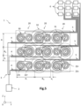
- FIGS. 4A and 4B are top views of two examples of Mach-Zehnder interferometer arrays 20, the arrangement of the interferometers 20 and the sensitive surfaces 30 of which is supposed to reduce the bulk of the interferometer array 20 while ensuring that the risk of coalescence of the microdroplets 31 is eliminated.
- the Mach-Zehnder interferometers 20 and the sensitive surfaces 30 have an identical arrangement, namely here a hexagonal periodic arrangement oriented here along the longitudinal axis Z.
- seven interferometers 20 are arranged at the vertices and in the center of a hexagon, including three interferometers 20 aligned along the longitudinal axis Z.
- the sensitive surfaces 30 are arranged on the same side of the longitudinal axis Z, namely here on the left side (direction -Y).
- the adjacent interferometers 20 of the same column are spaced by a distance substantially equal to d g +2 ⁇ p g , and here equal to 290 ⁇ m, while the distance separating two adjacent interferometers 20 of different columns is greater than d g +2 ⁇ p g , and here equal to 360 ⁇ m.
- the Mach-Zehnder interferometers 20 and the sensitive surfaces 30 does not lead to an optimization of the size of the interferometer matrix 20.
- the total surface area (dotted rectangular line) of the matrix is greater than that of the fig.2 by more than 15%, in particular due to the presence of non-useful empty areas.
- the interferometer lines 20 are no longer spaced from each other by a constant spacing e l , so that this arrangement greatly complicates the possible arrangement of the input 4 and output 5 waveguides.
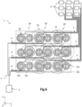
- the Mach-Zehnder interferometers 20 and the sensitive surfaces 30 also have an identical arrangement, namely here a hexagonal periodic arrangement. However, it is here oriented along the transverse axis Y (three interferometers 20 of the hexagon are aligned along the Y axis).
- the sensitive surfaces 30 are arranged on the same side of the longitudinal axis Z, namely here on the left side (direction -Y).
- This arrangement is also not a regular hexagon. Indeed, the adjacent interferometers 20 forming a side located on the same line are spaced from each other by a distance greater than d g +2 ⁇ p g , here equal to 330 ⁇ m. And the interferometers 20 forming a side that passes from one line to the other are spaced by a distance d g +2 ⁇ p g equal here to 290 ⁇ m.
- the interferometers 20 and the sensitive surfaces 30 does not lead to a real optimization of the size of the matrix of interferometers 20 either. Indeed, the total surface area of the matrix is only about 3% less than that of the fig.2 , due to unnecessary empty areas. Furthermore, the lines 20 interferometers are spaced from each other by a constant spacing e l of the order of 90 ⁇ m (compared to 140 ⁇ m in the fig.2 ).
- FIG. 5 is a schematic and partial top view of an interferometric detection system 1 according to one embodiment of the invention.
- the arrangement of the sensitive surfaces 30 differs from that of the fig.2 essentially by the arrangement of the sensitive surfaces 30. Indeed, it appears that dissociating the periodic arrangement of the interferometers 20 from that of the sensitive surfaces 30 makes it possible to reduce the size of the Mach-Zehnder interferometer matrix while ensuring that the microdroplets 31 cannot coalesce. In addition, the spacing between the rows and/or columns of the interferometers 20 is sufficient to allow the passage of the input 4 and output 5 waveguides.
- the Mach-Zehnder interferometers 20 are arranged in a rectangular periodic manner. They are aligned in rows along the transverse axis Y and are aligned in columns along the longitudinal axis Z.
- the transverse pitch p t is constant and is here equal to approximately 330 ⁇ m. It is formed by the transverse dimension d tb of the arms (here equal to approximately 300 ⁇ m) and the transverse spacing e t between the arms 22 of two adjacent interferometers 20 (here equal to approximately 30 ⁇ m).
- the longitudinal pitch p l is constant and is here equal to approximately 250 ⁇ m. It is formed by the longitudinal dimension d lb of the arms (here equal to approximately 150 ⁇ m) and the longitudinal spacing e l between the arms 22 of two adjacent interferometers 20 (here equal to approximately 100 ⁇ m).
- the sensitive surfaces 30 are arranged in a hexagonal periodic manner along the transverse axis Y. They are located on the six vertices and the center of the hexagon. The hexagon is oriented along the transverse axis Y in the sense that three sensitive surfaces 30 of the hexagon (two vertices and the center) are located on the same line and are aligned along the transverse axis Y.
- This hexagonal periodic arrangement results in the fact that the sensitive surfaces of the same line are positioned on the same side of the longitudinal axis Z passing between the two arms 22 of the interferometer 20 considered, and that this positioning side changes from one line to the other.
- the positioning side of the sensitive surfaces 30 with respect to the interferometers 20 of the same column alternates from one line to the other.
- the sensitive surfaces 30 of the lower line are located opposite the left arm 22 (located in the -Y direction)
- the sensitive surfaces 30 of the central line are located opposite the right arm 22 (located in the +Y direction)
- the sensitive surfaces 30 of the upper line are located opposite the left arm 22.
- the interferometers 20 in a rectangular manner makes it possible to avoid the unnecessary areas which appear in the fig.4A and 4B .
- the hexagonal periodic arrangement of the sensitive surfaces 30 makes it possible to reduce the size of the interferometer matrix since it is possible to reduce the spacings e l and/or e t while ensuring that the microdroplets 31 cannot coalesce on the one hand, and that the passage of the input 4 and output 5 waveguides remains possible on the other hand.
- the total surface area of the Mach-Zehnder interferometer matrix is almost 14% less than that of the fig.2 .
- the Mach-Zehnder 20 interferometers can have a symmetrical configuration from one line to another.
- the 20 interferometers have the configuration of the fig.5 , and for neighboring lines, the optical splitter 21 is located upstream of the center of the spiral arms 22 (along the -Z direction) while the optical coupler 23 is located downstream of the center of the spiral arms 22 (along the +Z direction).
- the arms 22 have a spiral and/or serpentine shape with an aspect ratio equal to 1 to 20% near.
Landscapes
- Physics & Mathematics (AREA)
- Chemical & Material Sciences (AREA)
- Pathology (AREA)
- General Health & Medical Sciences (AREA)
- Immunology (AREA)
- Health & Medical Sciences (AREA)
- Life Sciences & Earth Sciences (AREA)
- Analytical Chemistry (AREA)
- Biochemistry (AREA)
- General Physics & Mathematics (AREA)
- Chemical Kinetics & Catalysis (AREA)
- Plasma & Fusion (AREA)
- Engineering & Computer Science (AREA)
- Spectroscopy & Molecular Physics (AREA)
- Investigating Or Analysing Materials By Optical Means (AREA)
- Optical Integrated Circuits (AREA)
Claims (10)
- Interferometrisches System (1) zum Nachweisen von Analyten, die in einer Flüssigkeitsprobe vorhanden sind, Folgendes umfassend:∘ ein Anordnung von Mach-Zehnder-Interferometern (20), die dazu bestimmt ist, einerseits an mindestens eine Laserquelle (2) und andererseits an eine Vielzahl von Fotodetektoren (6) gekoppelt zu werden, wobei jedes Interferometer (20) zwei Wellenleiter (22) umfasst, die die Arme des Interferometers bilden, wobei sich die Arme (22) spiralförmig und/oder schlangenförmig mit einem Seitenverhältnis von 1 erstrecken,• wobei die Interferometer (20) periodisch und rechteckig angeordnet und in Spalten entlang einer Längsachse (Z), die zwischen den Armen (22) jedes Interferometers (20) verläuft, und in Zeilen entlang einer Querachse (Y), die orthogonal zur Längsachse (Z) verläuft, ausgerichtet sind;∘ eine Anordnung von empfindlichen Oberflächen (30), die jeweils aus Rezeptoren ausgebildet sind, mit denen die Analyten durch Adsorption/Desorption interagieren können, wobei jede empfindliche Oberfläche (30) mindestens teilweise einen der Arme (22) eines Interferometers (20) bedeckt, der dann einen empfindlichen Arm (22s) bildet, und den anderen Arm (22) nicht bedeckt, der dann einen Referenzarm (22r) bildet;∘ dadurch gekennzeichnet, dass:• die empfindlichen Oberflächen (30) periodisch und sechseckig angeordnet sind, so dass jede der empfindlichen Oberflächen (30) derselben Linie auf derselben Seite der Längsachse (Z) positioniert ist, die zwischen den beiden Armen (22) des betrachteten Interferometers (20) verläuft, wobei die Positionierungsseite der empfindlichen Oberflächen (30) gegenüber den Interferometern (20) derselben Spalte sich dann von einer Zeile zur anderen abwechseln.
- Interferometrisches System (1) nach Anspruch 1, wobei die empfindlichen Oberflächen (30) desselben Sechsecks drei empfindliche Oberflächen (30) umfassen, die entlang der Querachse (Y) ausgerichtet sind.
- Interferometrisches System (1) nach Anspruch 1 oder 2, wobei empfindliche Oberflächen (30) unterschiedliche Rezeptoren im Hinblick auf die chemische und/oder physikalische Affinität derjenigen der benachbarten empfindlichen Oberflächen umfassen.
- Interferometrisches System (1) nach einem der Ansprüche 1 bis 3, das Eingangswellenleiter (4) umfasst, die die Laserquelle (2) mit jedem Interferometer (20) koppeln, und Ausgangswellenleiter (5), die jedes Interferometer (20) mit den Fotodetektoren (6) koppeln, wobei sich die Eingangs- (5) und die Ausgangswellenleiter (6) entlang der Querachse (Y) zwischen jeder Linie der Interferometer (20) erstrecken.
- Interferometrisches System (1) nach einem der Ansprüche 1 bis 4, wobei die Arme (22) derselben Linie von denen der benachbarten Linie bzw. der benachbarten Linien um einen konstanten Längsabstand ei von einer Linie zur anderen beabstandet sind, und die Arme (22) derselben Spalte von denen der benachbarten Spalte bzw. der benachbarten Spalten um einen konstanten Querabstand et von einer Spalte zur anderen beabstandet sind.
- Interferometrisches System (1) nach einem der Ansprüche 1 bis 5, wobei die Arme (22) auf Siliziumbasis hergestellt sind und von einer Umhüllung umgeben ist, die aus einem Oxid hergestellt ist und einen niedrigen Brechungsindex im Vergleich zum Brechungsindex der Arme aufweist.
- Interferometrisches System (1) nach einem der Ansprüche 1 bis 6, wobei eine Umhüllung der Arme (22) durch eine untere Schicht und durch eine obere Schicht ausgebildet ist, wobei die obere Schicht an jedem empfindlichen Arm (22s) eine Aussparung aufweist.
- Interferometrisches System (1) nach den Ansprüchen 6 und 7, wobei die Arme (22) aus Siliziumnitrid hergestellt sind und mit einer dünnen Haftschicht (14), die aus einem Oxid hergestellt ist, bedeckt sind, auf der die Rezeptoren befestigt sind, wobei sich die dünne Haftschicht (14) in der Aussparung befindet.
- Interferometrisches System (1) nach Anspruch 8, das Organosilane umfasst, die auf die dünne Haftschicht (14) aufgepfropft sind und reaktive Gruppen bilden, an die die Rezeptoren gebunden sind.
- Verfahren zum Herstellen eines interferometrischen Systems (1) nach einem der vorhergehenden Ansprüche, das einen Schritt des Abscheidens von Mikrotröpfchen, die die Rezeptoren enthalten:∘ gegenüber den Armen (22) umfasst, die dazu bestimmt sind, die empfindlichen Arme (22s) zu bilden,∘ wobei die abgeschiedenen Mikrotröpfchen eine Abmessung dg in einer Ebene parallel zur Anordnung von Interferometern (20) aufweisen;∘ wobei das Abscheiden der Mikrotröpfchen eine Positionierungsunsicherheit Δpg ungleich Null aufweist, wobei die Arme (22), die dazu bestimmt sind, empfindliche Arme (22s) zu werden, dann paarweise um einen Abstand von mindestens gleich dg + 2 × Δpg voneinander beabstandet sind.
Applications Claiming Priority (3)
| Application Number | Priority Date | Filing Date | Title |
|---|---|---|---|
| FR2106153A FR3123988A1 (fr) | 2021-06-10 | 2021-06-10 | systeme interférométrique de detection d’analytes comportant une matrice d’interféromètres de Mach-Zehnder |
| FR2108208A FR3123987B1 (fr) | 2021-06-10 | 2021-07-28 | systeme interférométrique de detection d’analytes comportant une matrice d’interféromètres de Mach-Zehnder |
| PCT/EP2022/065307 WO2022258559A1 (fr) | 2021-06-10 | 2022-06-06 | Systeme interferometrique de detection d'analytes comportant une matrice d'interferometres de mach-zehnder |
Publications (3)
| Publication Number | Publication Date |
|---|---|
| EP4352492A1 EP4352492A1 (de) | 2024-04-17 |
| EP4352492B1 true EP4352492B1 (de) | 2025-01-01 |
| EP4352492C0 EP4352492C0 (de) | 2025-01-01 |
Family
ID=82115869
Family Applications (1)
| Application Number | Title | Priority Date | Filing Date |
|---|---|---|---|
| EP22731692.4A Active EP4352492B1 (de) | 2021-06-10 | 2022-06-06 | Interferometrisches analytnachweissystem mit mach-zehnder-interferometerarray |
Country Status (6)
| Country | Link |
|---|---|
| US (1) | US20240280495A1 (de) |
| EP (1) | EP4352492B1 (de) |
| JP (1) | JP2024520823A (de) |
| KR (1) | KR20240028425A (de) |
| TW (1) | TW202314224A (de) |
| WO (1) | WO2022258559A1 (de) |
Families Citing this family (2)
| Publication number | Priority date | Publication date | Assignee | Title |
|---|---|---|---|---|
| FR3122921B1 (fr) * | 2021-05-11 | 2026-01-23 | Aryballe | Dispositif électronique d’analyse d’un analyte présent dans un fluide comportant un capteur et procédé de remplacement du capteur |
| FR3153418B1 (fr) * | 2023-09-22 | 2025-10-10 | Commissariat Energie Atomique | Système analytique en phase gazeuse à dispositif de détection optique |
Family Cites Families (5)
| Publication number | Priority date | Publication date | Assignee | Title |
|---|---|---|---|---|
| US5173747A (en) * | 1990-09-20 | 1992-12-22 | Battelle Memorial Institute | Integrated optical directional-coupling refractometer apparatus |
| EP2400291A1 (de) * | 2010-06-17 | 2011-12-28 | Optisense B.V. | Integrierter Lichtwellenleiter-Evaneszenzfeldsensor und länglicher Abschnitt eines Substrats zur Verwendung in solch einem Sensor |
| FR3097640B1 (fr) | 2019-06-21 | 2021-07-02 | Commissariat Energie Atomique | Circuit optique intégré à bras de référence encapsulé |
| US20230133866A1 (en) * | 2020-04-09 | 2023-05-04 | SiPhox Inc. | Integrated photonic systems and methods for biosensing |
| WO2023003985A1 (en) * | 2021-07-20 | 2023-01-26 | Siphox, Inc. | Integrated silicon photonic biosensors for plate readers, and related systems and methods |
-
2022
- 2022-06-06 KR KR1020247000988A patent/KR20240028425A/ko active Pending
- 2022-06-06 EP EP22731692.4A patent/EP4352492B1/de active Active
- 2022-06-06 US US18/568,555 patent/US20240280495A1/en active Pending
- 2022-06-06 WO PCT/EP2022/065307 patent/WO2022258559A1/fr not_active Ceased
- 2022-06-06 JP JP2023575983A patent/JP2024520823A/ja active Pending
- 2022-06-10 TW TW111121651A patent/TW202314224A/zh unknown
Also Published As
| Publication number | Publication date |
|---|---|
| KR20240028425A (ko) | 2024-03-05 |
| TW202314224A (zh) | 2023-04-01 |
| JP2024520823A (ja) | 2024-05-24 |
| US20240280495A1 (en) | 2024-08-22 |
| WO2022258559A1 (fr) | 2022-12-15 |
| EP4352492A1 (de) | 2024-04-17 |
| EP4352492C0 (de) | 2025-01-01 |
Similar Documents
| Publication | Publication Date | Title |
|---|---|---|
| EP3754326B1 (de) | Integrierter optischer schaltkreis mit eingekapseltem referenzarm | |
| JP4699459B2 (ja) | 多重波長光センサー | |
| Kussrow et al. | Interferometric methods for label-free molecular interaction studies | |
| US20020172457A1 (en) | Coated optical microcavity resonator chemical sensor | |
| US8320718B2 (en) | Optical sensors and methods of making the same | |
| EP4352492B1 (de) | Interferometrisches analytnachweissystem mit mach-zehnder-interferometerarray | |
| JPH08510831A (ja) | 屈折率を測定する方法および装置 | |
| WO2007144313A1 (fr) | Composant optique fonctionnant en transmission en champ proche | |
| Ciminelli et al. | Silicon photonic biosensors | |
| FR3123987A1 (fr) | systeme interférométrique de detection d’analytes comportant une matrice d’interféromètres de Mach-Zehnder | |
| Cano-Velázquez et al. | Beyond Spectral Resolution in Nanophotonic Sensing: Picometer-Level Precision with Multispectral Readout | |
| Duval et al. | Interferometric waveguide biosensors based on Si-technology for point-of-care diagnostic | |
| FR3124592A1 (fr) | Système de mesure de type MEMS ou NEMS multicapteurs | |
| EP4060329B1 (de) | Optomechanischer sensor für die konzentration von arten in einem flüssigen medium | |
| WO2012168589A1 (fr) | Biocapteur photonique multi-cible, procede de fabrication et de preparation | |
| EP3486603B1 (de) | System zur umwandlung einer bewegung in eine optische phasenverschiebung | |
| EP2396642A1 (de) | System und vorrichtung zur optischen erkennung von partikeln mit einem array zur entkopplung optischer informationen sowie herstellungsverfahren dafür | |
| EP1554565B1 (de) | Integriertes lumineszenzlesegerät | |
| EP1300675A1 (de) | Optischer Sensor zum Nachweis mindestens einer chemischen Substanz und solche Sensoren enthaltende optische Sonden | |
| WO2021140302A1 (fr) | Capteur pour détecter un analyte cible dans un milieu liquide avec un résonateur optique couplé à un résonateur mecanique | |
| Werquin et al. | Silicon Ring Resonator-Based Biochips | |
| FR3130845A1 (fr) | Dispositif de séquençage d’une sequence de nucleotides présentant une sensibilité augmentée et une fiabilité améliorée | |
| FR3134894A1 (fr) | procede de caractérisation d’analytes comportant une variation de température au moyen d’un nez électronique de type interferometrique | |
| FR3139389A1 (fr) | Système interférométrique de caractérisation calibré et présentant un encombrement réduit | |
| Lawrie et al. | Silicon Photonics for Biosensing Applications |
Legal Events
| Date | Code | Title | Description |
|---|---|---|---|
| STAA | Information on the status of an ep patent application or granted ep patent |
Free format text: STATUS: UNKNOWN |
|
| STAA | Information on the status of an ep patent application or granted ep patent |
Free format text: STATUS: THE INTERNATIONAL PUBLICATION HAS BEEN MADE |
|
| PUAI | Public reference made under article 153(3) epc to a published international application that has entered the european phase |
Free format text: ORIGINAL CODE: 0009012 |
|
| STAA | Information on the status of an ep patent application or granted ep patent |
Free format text: STATUS: REQUEST FOR EXAMINATION WAS MADE |
|
| 17P | Request for examination filed |
Effective date: 20231208 |
|
| AK | Designated contracting states |
Kind code of ref document: A1 Designated state(s): AL AT BE BG CH CY CZ DE DK EE ES FI FR GB GR HR HU IE IS IT LI LT LU LV MC MK MT NL NO PL PT RO RS SE SI SK SM TR |
|
| GRAP | Despatch of communication of intention to grant a patent |
Free format text: ORIGINAL CODE: EPIDOSNIGR1 |
|
| STAA | Information on the status of an ep patent application or granted ep patent |
Free format text: STATUS: GRANT OF PATENT IS INTENDED |
|
| DAV | Request for validation of the european patent (deleted) | ||
| DAX | Request for extension of the european patent (deleted) | ||
| INTG | Intention to grant announced |
Effective date: 20240916 |
|
| RAP3 | Party data changed (applicant data changed or rights of an application transferred) |
Owner name: ARYBALLE Owner name: COMMISSARIAT A L'ENERGIE ATOMIQUE ET AUX ENERGIESALTERNATIVES |
|
| GRAS | Grant fee paid |
Free format text: ORIGINAL CODE: EPIDOSNIGR3 |
|
| GRAA | (expected) grant |
Free format text: ORIGINAL CODE: 0009210 |
|
| STAA | Information on the status of an ep patent application or granted ep patent |
Free format text: STATUS: THE PATENT HAS BEEN GRANTED |
|
| AK | Designated contracting states |
Kind code of ref document: B1 Designated state(s): AL AT BE BG CH CY CZ DE DK EE ES FI FR GB GR HR HU IE IS IT LI LT LU LV MC MK MT NL NO PL PT RO RS SE SI SK SM TR |
|
| REG | Reference to a national code |
Ref country code: GB Ref legal event code: FG4D Free format text: NOT ENGLISH |
|
| REG | Reference to a national code |
Ref country code: DE Ref legal event code: R096 Ref document number: 602022009405 Country of ref document: DE |
|
| REG | Reference to a national code |
Ref country code: CH Ref legal event code: EP |
|
| REG | Reference to a national code |
Ref country code: IE Ref legal event code: FG4D Free format text: LANGUAGE OF EP DOCUMENT: FRENCH |
|
| U01 | Request for unitary effect filed |
Effective date: 20250122 |
|
| U07 | Unitary effect registered |
Designated state(s): AT BE BG DE DK EE FI FR IT LT LU LV MT NL PT RO SE SI Effective date: 20250129 |
|
| PG25 | Lapsed in a contracting state [announced via postgrant information from national office to epo] |
Ref country code: PL Free format text: LAPSE BECAUSE OF FAILURE TO SUBMIT A TRANSLATION OF THE DESCRIPTION OR TO PAY THE FEE WITHIN THE PRESCRIBED TIME-LIMIT Effective date: 20250101 |
|
| PG25 | Lapsed in a contracting state [announced via postgrant information from national office to epo] |
Ref country code: ES Free format text: LAPSE BECAUSE OF FAILURE TO SUBMIT A TRANSLATION OF THE DESCRIPTION OR TO PAY THE FEE WITHIN THE PRESCRIBED TIME-LIMIT Effective date: 20250101 |
|
| PG25 | Lapsed in a contracting state [announced via postgrant information from national office to epo] |
Ref country code: NO Free format text: LAPSE BECAUSE OF FAILURE TO SUBMIT A TRANSLATION OF THE DESCRIPTION OR TO PAY THE FEE WITHIN THE PRESCRIBED TIME-LIMIT Effective date: 20250401 Ref country code: IS Free format text: LAPSE BECAUSE OF FAILURE TO SUBMIT A TRANSLATION OF THE DESCRIPTION OR TO PAY THE FEE WITHIN THE PRESCRIBED TIME-LIMIT Effective date: 20250501 |
|
| PG25 | Lapsed in a contracting state [announced via postgrant information from national office to epo] |
Ref country code: HR Free format text: LAPSE BECAUSE OF FAILURE TO SUBMIT A TRANSLATION OF THE DESCRIPTION OR TO PAY THE FEE WITHIN THE PRESCRIBED TIME-LIMIT Effective date: 20250101 |
|
| PG25 | Lapsed in a contracting state [announced via postgrant information from national office to epo] |
Ref country code: GR Free format text: LAPSE BECAUSE OF FAILURE TO SUBMIT A TRANSLATION OF THE DESCRIPTION OR TO PAY THE FEE WITHIN THE PRESCRIBED TIME-LIMIT Effective date: 20250402 |
|
| PG25 | Lapsed in a contracting state [announced via postgrant information from national office to epo] |
Ref country code: CZ Free format text: LAPSE BECAUSE OF FAILURE TO SUBMIT A TRANSLATION OF THE DESCRIPTION OR TO PAY THE FEE WITHIN THE PRESCRIBED TIME-LIMIT Effective date: 20250101 |
|
| U20 | Renewal fee for the european patent with unitary effect paid |
Year of fee payment: 4 Effective date: 20250627 |
|
| PG25 | Lapsed in a contracting state [announced via postgrant information from national office to epo] |
Ref country code: SM Free format text: LAPSE BECAUSE OF FAILURE TO SUBMIT A TRANSLATION OF THE DESCRIPTION OR TO PAY THE FEE WITHIN THE PRESCRIBED TIME-LIMIT Effective date: 20250101 |
|
| PG25 | Lapsed in a contracting state [announced via postgrant information from national office to epo] |
Ref country code: SK Free format text: LAPSE BECAUSE OF FAILURE TO SUBMIT A TRANSLATION OF THE DESCRIPTION OR TO PAY THE FEE WITHIN THE PRESCRIBED TIME-LIMIT Effective date: 20250101 |
|
| PLBE | No opposition filed within time limit |
Free format text: ORIGINAL CODE: 0009261 |
|
| STAA | Information on the status of an ep patent application or granted ep patent |
Free format text: STATUS: NO OPPOSITION FILED WITHIN TIME LIMIT |
|
| REG | Reference to a national code |
Ref country code: CH Ref legal event code: L10 Free format text: ST27 STATUS EVENT CODE: U-0-0-L10-L00 (AS PROVIDED BY THE NATIONAL OFFICE) Effective date: 20251112 |
|
| U1N | Appointed representative for the unitary patent procedure changed after the registration of the unitary effect |
Representative=s name: SANTARELLI; FR |
|
| 26N | No opposition filed |
Effective date: 20251002 |
|
| REG | Reference to a national code |
Ref country code: CH Ref legal event code: H13 Free format text: ST27 STATUS EVENT CODE: U-0-0-H10-H13 (AS PROVIDED BY THE NATIONAL OFFICE) Effective date: 20260127 |
|
| PG25 | Lapsed in a contracting state [announced via postgrant information from national office to epo] |
Ref country code: MC Free format text: LAPSE BECAUSE OF FAILURE TO SUBMIT A TRANSLATION OF THE DESCRIPTION OR TO PAY THE FEE WITHIN THE PRESCRIBED TIME-LIMIT Effective date: 20250101 |