EP4350989A1 - Slew-rate boost circuitry - Google Patents
Slew-rate boost circuitry Download PDFInfo
- Publication number
- EP4350989A1 EP4350989A1 EP23191905.1A EP23191905A EP4350989A1 EP 4350989 A1 EP4350989 A1 EP 4350989A1 EP 23191905 A EP23191905 A EP 23191905A EP 4350989 A1 EP4350989 A1 EP 4350989A1
- Authority
- EP
- European Patent Office
- Prior art keywords
- output
- voltage
- transistor
- input
- boost
- Prior art date
- Legal status (The legal status is an assumption and is not a legal conclusion. Google has not performed a legal analysis and makes no representation as to the accuracy of the status listed.)
- Pending
Links
Images




Classifications
-
- H—ELECTRICITY
- H03—ELECTRONIC CIRCUITRY
- H03F—AMPLIFIERS
- H03F3/00—Amplifiers with only discharge tubes or only semiconductor devices as amplifying elements
- H03F3/45—Differential amplifiers
- H03F3/45071—Differential amplifiers with semiconductor devices only
- H03F3/45076—Differential amplifiers with semiconductor devices only characterised by the way of implementation of the active amplifying circuit in the differential amplifier
- H03F3/45179—Differential amplifiers with semiconductor devices only characterised by the way of implementation of the active amplifying circuit in the differential amplifier using MOSFET transistors as the active amplifying circuit
- H03F3/45273—Mirror types
-
- H—ELECTRICITY
- H03—ELECTRONIC CIRCUITRY
- H03F—AMPLIFIERS
- H03F1/00—Details of amplifiers with only discharge tubes, only semiconductor devices or only unspecified devices as amplifying elements
- H03F1/02—Modifications of amplifiers to raise the efficiency, e.g. gliding Class A stages, use of an auxiliary oscillation
- H03F1/0205—Modifications of amplifiers to raise the efficiency, e.g. gliding Class A stages, use of an auxiliary oscillation in transistor amplifiers
-
- H—ELECTRICITY
- H03—ELECTRONIC CIRCUITRY
- H03F—AMPLIFIERS
- H03F1/00—Details of amplifiers with only discharge tubes, only semiconductor devices or only unspecified devices as amplifying elements
- H03F1/02—Modifications of amplifiers to raise the efficiency, e.g. gliding Class A stages, use of an auxiliary oscillation
- H03F1/0205—Modifications of amplifiers to raise the efficiency, e.g. gliding Class A stages, use of an auxiliary oscillation in transistor amplifiers
- H03F1/0211—Modifications of amplifiers to raise the efficiency, e.g. gliding Class A stages, use of an auxiliary oscillation in transistor amplifiers with control of the supply voltage or current
-
- H—ELECTRICITY
- H03—ELECTRONIC CIRCUITRY
- H03F—AMPLIFIERS
- H03F1/00—Details of amplifiers with only discharge tubes, only semiconductor devices or only unspecified devices as amplifying elements
- H03F1/26—Modifications of amplifiers to reduce influence of noise generated by amplifying elements
-
- H—ELECTRICITY
- H03—ELECTRONIC CIRCUITRY
- H03F—AMPLIFIERS
- H03F1/00—Details of amplifiers with only discharge tubes, only semiconductor devices or only unspecified devices as amplifying elements
- H03F1/32—Modifications of amplifiers to reduce non-linear distortion
-
- H—ELECTRICITY
- H03—ELECTRONIC CIRCUITRY
- H03F—AMPLIFIERS
- H03F3/00—Amplifiers with only discharge tubes or only semiconductor devices as amplifying elements
- H03F3/30—Single-ended push-pull [SEPP] amplifiers; Phase-splitters therefor
- H03F3/3001—Single-ended push-pull [SEPP] amplifiers; Phase-splitters therefor with field-effect transistors
- H03F3/3022—CMOS common source output SEPP amplifiers
-
- H—ELECTRICITY
- H03—ELECTRONIC CIRCUITRY
- H03F—AMPLIFIERS
- H03F3/00—Amplifiers with only discharge tubes or only semiconductor devices as amplifying elements
- H03F3/45—Differential amplifiers
-
- H—ELECTRICITY
- H03—ELECTRONIC CIRCUITRY
- H03F—AMPLIFIERS
- H03F3/00—Amplifiers with only discharge tubes or only semiconductor devices as amplifying elements
- H03F3/45—Differential amplifiers
- H03F3/45071—Differential amplifiers with semiconductor devices only
- H03F3/45076—Differential amplifiers with semiconductor devices only characterised by the way of implementation of the active amplifying circuit in the differential amplifier
- H03F3/45179—Differential amplifiers with semiconductor devices only characterised by the way of implementation of the active amplifying circuit in the differential amplifier using MOSFET transistors as the active amplifying circuit
- H03F3/45183—Long tailed pairs
-
- H—ELECTRICITY
- H03—ELECTRONIC CIRCUITRY
- H03F—AMPLIFIERS
- H03F3/00—Amplifiers with only discharge tubes or only semiconductor devices as amplifying elements
- H03F3/45—Differential amplifiers
- H03F3/45071—Differential amplifiers with semiconductor devices only
- H03F3/45076—Differential amplifiers with semiconductor devices only characterised by the way of implementation of the active amplifying circuit in the differential amplifier
- H03F3/45179—Differential amplifiers with semiconductor devices only characterised by the way of implementation of the active amplifying circuit in the differential amplifier using MOSFET transistors as the active amplifying circuit
- H03F3/4521—Complementary long tailed pairs having parallel inputs and being supplied in parallel
-
- H—ELECTRICITY
- H03—ELECTRONIC CIRCUITRY
- H03F—AMPLIFIERS
- H03F3/00—Amplifiers with only discharge tubes or only semiconductor devices as amplifying elements
- H03F3/45—Differential amplifiers
- H03F3/45071—Differential amplifiers with semiconductor devices only
- H03F3/45076—Differential amplifiers with semiconductor devices only characterised by the way of implementation of the active amplifying circuit in the differential amplifier
- H03F3/45475—Differential amplifiers with semiconductor devices only characterised by the way of implementation of the active amplifying circuit in the differential amplifier using IC blocks as the active amplifying circuit
-
- H—ELECTRICITY
- H03—ELECTRONIC CIRCUITRY
- H03F—AMPLIFIERS
- H03F2203/00—Indexing scheme relating to amplifiers with only discharge tubes or only semiconductor devices as amplifying elements covered by H03F3/00
- H03F2203/45—Indexing scheme relating to differential amplifiers
- H03F2203/45248—Indexing scheme relating to differential amplifiers the dif amp being designed for improving the slew rate
-
- H—ELECTRICITY
- H03—ELECTRONIC CIRCUITRY
- H03F—AMPLIFIERS
- H03F2203/00—Indexing scheme relating to amplifiers with only discharge tubes or only semiconductor devices as amplifying elements covered by H03F3/00
- H03F2203/45—Indexing scheme relating to differential amplifiers
- H03F2203/45392—Indexing scheme relating to differential amplifiers the AAC comprising resistors in the source circuit of the AAC before the common source coupling
Definitions
- Slew-rate may be the measure of how fast an operational amplifier can charge the output capacitance.
- a high value for the slew-rate may increase the performance of the operational amplifier but can also increase power consumption and/or affect other performance parameters such as bandwidth and noise.
- the techniques described herein relate to a circuit including an operational amplifier that includes a differential amplifier, a capacitor, and an output stage.
- the differential amplifier includes a first input and a second input.
- the output stage is configured to generate an output voltage.
- the circuit includes a slew-rate boost circuitry connected to the operational amplifier.
- the slew-rate boost circuitry is configured to detect a voltage differential between the first input and the second input and apply, at an output of the differential amplifier, a boost current to charge the capacitor during a period of time in which the output voltage increases or decreases to a target voltage level.
- the techniques described herein relate to a circuit including an operational amplifier that includes a differential amplifier, a capacitor, and an output stage.
- the output stage configured to generate an output voltage
- a first control circuitry configured to apply, at an output of the differential amplifier, a first boost current to charge the capacitor during a first period of time in which the output voltage increases from a first voltage level to a second voltage level
- a second control circuitry configured to apply, at the output of the differential amplifier, a second boost current to charge the capacitor during a second period of time in which the output voltage decreases from the second voltage level to the first voltage level.
- the techniques described herein relate to a method for increasing a slew-rate of an operational amplifier, the method including detecting a first voltage differential between a first input of a differential amplifier and a second input of the differential amplifier, applying, at an output of the differential amplifier, a first boost current to charge a capacitor during a first period of time in which an output voltage increases from a first voltage level to a second voltage level, detecting a second voltage differential between the first input and the second input, and applying, at the output of the differential amplifier, a second boost current to charge the capacitor during a second period of time in which the output voltage decreases from the second voltage level to the first voltage level.
- This description relates to a slew-rate boost circuitry configured to increase a current applied to an operational amplifier during a slew condition, thereby reducing the amount of time to charge an output voltage of the operational amplifier to a target voltage level.
- the slew-rate boost circuitry is configured to add a boost current to increase the slew-rate during the transient response of the operational amplifier.
- the operational amplifier may include a differential amplifier, an output stage coupled to an output of the differential amplifier, and one or more output capacitances coupled to the output of the differential amplifier or the output stage.
- the slew-rate boost circuitry includes a first control circuitry and a second control circuitry.
- the first control circuitry is configured to apply a first boost current to increase a positive voltage slope (e.g., a rising edge slope), and the second control circuitry 106 is configured to apply a second boost current to increase a negative voltage slope (e.g., a falling edge slope). Since the slew-rate boost circuitry independently monitors and controls the positive voltage slope and the negative voltage slope (e.g., via the first control circuitry and the second control circuitry), the response time of the operational amplifier can be improved while minimizing the effect on other parameters such as noise and bandwidth.
- the first control circuitry is connected to the output of the differential amplifier.
- the first control circuitry is configured to apply, at the output of the differential amplifier, the first boost current to charge the output capacitance(s) during the slewing operation (e.g., during the period of time in which the output voltage increases from a first voltage level to a second voltage level).
- the first boost current may increase the positive voltage slope (e.g., the slew-rate) such that the output capacitance(s) are charged faster.
- the first control circuitry may remove the first boost current (e.g., provide a first boost current of zero or substantially zero). In other words, the first boost current may be applied during the transient response of the operational amplifier.
- the quiescent current may be minimized.
- a slew-rate value may be proportional (e.g., directly proportional) to the quiescent current of a circuit that includes an operational amplifier.
- the slew-rate boost circuitry may increase the slew-rate while minimizing the quiescent current in the operational amplifier.
- the second control circuitry is connected to the output of the differential amplifier.
- the second control circuitry is configured to apply, at the output of the differential amplifier, the second boost current to charge the output capacitance(s) during the slewing operation (e.g., during the period of time in which the output voltage decreases from the second voltage level to the first voltage level).
- the second boost current may increase the negative voltage slope (e.g., the slew-rate) such that the output capacitance(s) are charged faster.
- the second control circuitry may remove the second boost current (e.g., provide a second boost current of zero or substantially zero).
- the second boost current may be applied during the transient response of the operational amplifier. Similar to the first boost current, since the second boost current is applied during the transient response, the quiescent current may be minimized in the operational amplifier.
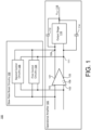
- FIG. 1 illustrates a circuit 100 for increasing the slew-rate of an operational amplifier 105 according to an aspect.
- the slew-rate may be the measure of how fast the operational amplifier 105 can charge output capacitances (e.g., capacitor 112, capacitor 114).
- the circuit 100 may apply a boost current to increase the rate at which the output capacitances are charged, where the boost current is applied when the operational amplifier 105 is active.
- the operational amplifier 105 may be active when the output voltage 116 is changing in response to a change to the input voltage. In other words, the operational amplifier 105 may be active during a transient response of the operational amplifier 105 (e.g., during a slewing operation).
- the circuit 100 may remove the boost current when the operational amplifier 105 is not active (e.g., in a steady-state mode).
- the operational amplifier 105 may be in a non-active state when an equilibrium between the input and the output is achieved (e.g., no further voltage movements).
- the circuit 100 may selectively apply the boost current during (e.g., only during) the transient response of the operational amplifier 105, the quiescent current (IQ) of the circuit 100 may be reduced, which can reduce power consumption.
- the boost current may be applied at an output of a differential amplifier 108 or an output stage 110 of the operational amplifier 105, which can reduce noise and/or distortion within the circuit 100.
- the circuit 100 may be used in a wide variety of devices such as analog-to-digital converters (ADCs), digital-to-analog converters (DACs), buffers, or regulated power supplies.
- the operational amplifier 105 includes a differential amplifier 108, an output stage 110, a capacitor 112, and a capacitor 114.
- the differential amplifier 108 includes a first input 101 and a second input 103.
- the differential amplifier 108 is configured to amplify the voltage difference between the first input 101 and the second input 103.
- the first input 101 is an inverting input.
- the second input 103 is a non-inverting input.
- a voltage differential between the first input 101 and the second input 103 may represent an input signal.
- the output stage 110 is connected to the differential amplifier 108.
- the output stage 110 is configured to generate the output voltage 116 (e.g., the output of the output stage 110 is the output voltage 116).
- the output stage 110 may include one or more electrical components such as transistor(s), amplifier(s), and/or voltage/current source(s).
- the topology of the output stage 110 may widely vary depending on the implementation of the circuit 100.
- the differential amplifier 108 includes a first output 121 and a second output 123. Similar to the first input 101 and the second input 103, the first output 121 and the second output 123 are differential. In some examples, the differential amplifier 108 is referred to as fully differential. In some examples, the first output 121 is a positive output. In some examples, the second output 123 is a negative output. The output voltages of the differential amplifier 108 may be equal but opposite in polarity. The first output 121 is connected to the input of the output stage 110. The second output 123 is connected to the input of the output stage 110.
- the capacitor 112 and the capacitor 114 may be the output capacitances.
- the capacitor 112 and the capacitor 114 may represent compensation and/or parasitic capacitances.
- the capacitor 112 is connected in parallel with the output stage 110.
- the capacitor 112 has a first terminal connected to the input of the output stage 110 and a second terminal connected to the output of the output stage 110.
- the first terminal of the capacitor 112 may be also connected to the first output 121.
- the capacitor 114 is connected in parallel with the output stage 110.
- the capacitor 114 has a first terminal connected to the input of the output stage 110 and a second terminal connected to the output of the output stage 110.
- the first terminal of the capacitor 112 may be also connected to the second output 123.
- the operational amplifier 105 may receive an input voltage and generate an output voltage 116 that corresponds to the input voltage. For example, if the input voltage changes from a threshold voltage (e.g., a first voltage level such as zero volts) to a higher voltage level (e.g., a second voltage level such as five volts), the operational amplifier 105 increases the output voltage 116 from the first voltage level to the second voltage level and the slew-rate is the time to change the output voltage 116 from the first voltage level to the second voltage level (e.g., rising edge slope).
- a threshold voltage e.g., a first voltage level such as zero volts
- a higher voltage level e.g., a second voltage level such as five volts
- the operational amplifier 105 increases the output voltage 116 from the first voltage level to the second voltage level and the slew-rate is the time to change the output voltage 116 from the first voltage level to the second voltage level (e.g., rising edge slope).
- the operational amplifier 105 decreases the output voltage 116 from the second voltage level to the first voltage level and the slew-rate is the time to change the output voltage 116 from the second voltage level to the first voltage level (e.g., falling edge slope).
- the operational amplifier 105 converts the output voltage 116 from the first voltage level to the second voltage level (e.g., rising edge slope), which may be referred to as the transient response of the operational amplifier 105.
- the operational amplifier 105 converts the output voltage 116 from the second voltage level to the first voltage level (e.g., falling edge slope), which may also be referred to as the transient response of the operational amplifier 105.
- the second threshold level is the same as the first threshold level. In some examples, the second threshold level is different from the first threshold level.
- the circuit 100 includes slew-rate boost circuitry 102 configured to add a boost current to increase the slew-rate during the transient response of the operational amplifier 105.
- the design of the slew-rate boost circuitry 102 is relatively small, which occupies a relatively small space in a converter, thereby reducing or eliminating compensation capacitors.
- the slew-rate boost circuitry 102 can be used for low voltage or high voltage operational amplifiers.
- the slew-rate boost circuitry 102 may increase the slew-rate of the operational amplifier 105 without significantly increasing the overall quiescent current.
- the slew-rate boost circuitry 102 may be used with any type of operational amplifier topology.
- the slew-rate boost circuitry 102 includes a first control circuitry 104 and a second control circuitry 106.
- the first control circuitry 104 is configured to apply a boost current to increase the positive voltage slope (e.g., rising edge slope)
- the second control circuitry 106 is configured to apply a boost current to increase the negative voltage slope (e.g., falling edge slope).
- the positive voltage slope may be a first slew-rate and the negative voltage slope may be a second slew-rate.
- the slew-rate boost circuitry 102 independently monitors and controls the positive and negative voltage slopes (e.g., via the first control circuitry 104 and the second control circuitry 106), the response time of the operational amplifier 105 can be improved while minimizing the effect on other parameters such as noise and bandwidth.
- the first control circuitry 104 is connected to the first input 101 and the second input 103 of the differential amplifier 108.
- the first control circuitry 104 is configured to measure the voltage differential between the first input 101 and the second input 103 and detect a slewing condition, e.g., whether the voltage differential between the first input 101 and the second input 103 exceeds a threshold level. In some examples, the first control circuitry 104 detects whether the voltage differential is positive (e.g., increasing), and, in some examples, greater than a first voltage threshold.
- the first control circuitry 104 may be connected to the output of the differential amplifier 108.
- the first control circuitry 104 may be connected to the input of the output stage 110.
- the first control circuitry 104 is connected to the first output 121 of the differential amplifier 108 and connected to the second output 123 of the differential amplifier 108. In some examples, the first control circuitry 104 is connected to a node 109, where the node 109 is connected to the first output 121 and the input of the output stage 110. In some examples, the first control circuitry 104 is connected to a node 111, where the node 111 is connected to the first output 121 and the input of the output stage 110.
- the first control circuitry 104 is configured to apply, at the output of the differential amplifier 108, a boost current (e.g., a first boost current) to charge the output capacitances (e.g., the capacitor 112 and/or the capacitor 114) during the slewing operation (e.g., during the period of time in which the output voltage increases to the second voltage level).
- the boost current may increase the positive voltage slope (e.g., the slew-rate) such that the output capacitances are charged faster.
- the first control circuitry 104 may remove the boost current. In other words, the boost current may be applied during the transient response of the operational amplifier 105.
- the second control circuitry 106 is connected to the first input 101 and the second input 103 of the differential amplifier 108.
- the second control circuitry 106 is configured to measure the voltage differential between the first input 101 and the second input 103 and detect a slewing condition, e.g., whether the voltage differential between the first input 101 and the second input 103 exceeds a second voltage threshold.
- the second control circuitry 106 is configured to detect whether the voltage differential is negative (e.g., decreasing) and, in some examples, greater than the second voltage threshold.
- the second control circuitry 106 may be connected to the output of the differential amplifier 108.
- the second control circuitry 106 may be connected to the input of the output stage 110.
- the second control circuitry 106 is connected to the first output 121 of the differential amplifier 108 and connected to the second output 123 of the differential amplifier 108. In some examples, the second control circuitry 106 is connected to a node 109, where the node 109 is connected to the first output 121 and the input of the output stage 110. In some examples, the second control circuitry 106 is connected to a node 111, where the node 111 is connected to the first output 121 and the input of the output stage 110.
- the second control circuitry 106 is configured to apply, at the output of the differential amplifier 108, a boost current (e.g., a second boost current) to charge the output capacitances (e.g., the capacitor 112 and/or the capacitor 114) during the slewing operation (e.g., during the period of time in which the output voltage decreases to the first voltage level).
- the boost current may increase the negative voltage slope such that the output capacitances are charged faster.
- the second control circuitry 106 may remove the boost current.
- the boost current may be applied during the transient response of the operational amplifier 105.
- FIG. 2 illustrates an example of a first control circuitry 204 according to an aspect.
- the first control circuitry 204 may be an example of the first control circuitry 104 of FIG. 1 and may include any of the details discussed with that figure.
- the first control circuitry 204 includes a differential voltage detector 220, a sense amplifier 236, and a current mirror 251.
- the current mirror 251 is configured to generate the boost current, which is provided to the node 109 of FIG. 1 and the node 111 of FIG. 1 .
- the differential voltage detector 220 is configured to detect the voltage differential between the first input 101 of FIG. 1 and the second input 103 of FIG. 1 and determine a slewing condition, e.g., whether the voltage differential between the first input 101 of FIG. 1 and the second input 103 of FIG. 1 is positive, and, in some examples, exceeds a first voltage threshold.
- the differential voltage detector 220 includes a transistor 226, a transistor 228, a resistor 230, a resistor 232, a resistor 222, a resistor 224, and a voltage source VDD.
- the voltage source VDD is included in the first control circuitry 204.
- the voltage source VDD is an external source voltage (e.g., a voltage that is received by the first control circuitry 204). In some examples, the voltage source VDD is a positive supply voltage. In some examples, the transistor 226 includes a N-type transistor. In some examples, the transistor 228 includes a N-type transistor.
- the gate of the transistor 226 is connected to the first input 101 of FIG. 1 , the drain of the transistor 226 is connected to a first terminal of the resistor 222, and the source of the transistor 226 is connected to the sense amplifier 236.
- the gate of the transistor 228 is connected to the second input 103 of FIG. 1 , the drain of the transistor 228 is connected to a first terminal of the resistor 224, and the source of the transistor 228 is connected to the sense amplifier 236.
- the source of the transistor 226 is connected to a first terminal of the resistor 230, and the source of the transistor 228 is connected to a first terminal of the resistor 232.
- a second terminal of the resistor 230 is connected to a second terminal of the resistor 232.
- the transistor 226, the transistor 228, the resistor 230, and the resistor 232 are used for reading the differential voltage and to determine a slewing event.
- imbalanced currents through the transistor 226 and the transistor 228 indicate an imbalance between the voltage drop across the resistor 230 and the resistor 232.x
- the sense amplifier 236 is configured to detect the voltage difference.
- the sense amplifier 236 includes a transistor 238, a transistor 240, a transistor 241, a current source 242, and a current source 244.
- the transistor 238 is a P-type transistor.
- the transistor 240 is a P-type transistor.
- the transistor 241 is a P-type transistor.
- the source of the transistor 238 is connected to the source of transistor 228, the drain of the transistor 238 is connected to the current source 244, and the gate of the transistor 238 is connected to the gate of the transistor 240. Also, the drain of the transistor 238 is connected to the gate of the transistor 238. Also, the source of the transistor 238 is connected to the source of the transistor 241.
- the source of the transistor 240 is connected to the source of the transistor 226, the drain of the transistor 240 is connected to the current source 242, and the gate of the transistor 240 is connected to the gate of the transistor 238. Also, the drain of the transistor 240 is connected to the gate of the transistor 241.
- the source of the transistor 241 is connected to the source of the transistor 228, the drain of the transistor 241 is connected to a drain of a transistor 246, and the gate of the transistor 241 is connected to the drain of the transistor 240.
- the first control circuitry 204 includes a current source 234.
- the current source 234 is connected to a node 231 disposed between the resistor 230 and the resistor 232.
- the current source 234 is also connected to a supply voltage VSS.
- the supply voltage VSS is connected to the current source 242 and the current source 244.
- the first control circuitry 204 includes a transistor 246.
- the transistor 246 is an N-type transistor.
- the drain of the transistor 246 is connected to the drain of the transistor 241, the source of the transistor 246 is connected to the supply voltage VSS, and the gate of the transistor 246 is connected to the drain of the transistor 246 and the gates of transistor 248 and the transistor 250.
- the inputs of the sense amplifier 236 are the sources of the transistor 240 and the transistor 238 and are connected to the sources of the transistor 226 and the transistor 228.
- the output of the sense amplifier 236 is the source of the transistor 241 and is connected to one of the inputs of the sense amplifier 236, so that a negative feedback loop is created. To assure the stability of the negative feedback loop, source inputs and source output are used.
- the current generated through the transistor 241 is mirrored by the current mirror 251 and provided to the node 109 and the node 111 of FIG. 1 .
- the output of the current mirror 251 is the boost current that is provided to the node 109 and the node 111 of FIG. 1 .
- the current mirror 251 includes a transistor 248 and a transistor 250.
- transistor 248 is a N-type transistor.
- the transistor 250 is a N-type transistor.
- the drain of the transistor 248 is connected to the node 109, the source of the transistor 248 is connected to the supply voltage VSS, and the gate of the transistor 248 is connected to the gates of the transistor 246 and the transistor 250, as well as the drain of the transistor 241.
- the drain of the transistor 250 is connected to the node 111 of FIG. 1 , the source of the transistor 250 is connected to the supply voltage VSS, and the gate of the transistor 250 is connected to the gates of the transistor 246 and the transistor 248, as well as the drain of the transistor 241.
- the first control circuitry 204 may embed hysteresis at one or more locations in the first control circuitry 204. By embedding hysteresis in the first control circuitry 204, the first control circuitry 204 may be activated for controlled differential voltages (e.g., V diff >100mV). In some examples, the values for current source 242 and the current source 244 are different (e.g., mismatched) in order to create hysteresis. In some examples, hysteresis can be created by using different values for the transistor 238 and the transistor 240 or different values for the resistor 230 and the resistor 232. It is noted that the purpose of the hysteresis may be to activate the first control circuitry 204 in the event of relatively high differential voltage steps and to reduce the activation caused by noise or small signals.
- V diff controlled differential voltages
- the values for current source 242 and the current source 244 are different (e.g., mismatched) in order to create hystere
- FIG. 3 illustrates an example of a second control circuitry 306 according to an aspect.
- the second control circuitry 306 may be an example of the second control circuitry 106 of FIG. 1 and may include any of the details discussed with that figure.
- the second control circuitry 306 includes a differential voltage detector 320, a sense amplifier 336, and a current mirror 351.
- the current mirror 351 is configured to generate the boost current, which is provided to the node 109 of FIG. 1 and the node 111 of FIG. 1 .
- the differential voltage detector 320 is configured to detect the voltage differential between the first input 101 of FIG. 1 and the second input 103 of FIG. 1 and determine a slewing condition, e.g., whether the voltage differential between the first input 101 of FIG. 1 and the second input 103 of FIG. 1 is negative and exceeds a threshold level.
- the differential voltage detector 220 includes a transistor 326, a transistor 328, a resistor 330, a resistor 332, a resistor 322, a resistor 324, and a voltage source VDD.
- the transistor 326 includes a P-type transistor.
- the transistor 328 includes a P-type transistor.
- the gate of the transistor 326 is connected to the first input 101 of FIG. 1 , the drain of the transistor 326 is connected to a first terminal of the resistor 322, and the source of the transistor 326 is connected to the sense amplifier 336.
- the gate of the transistor 328 is connected to the second input 103 of FIG. 1 , the drain of the transistor 328 is connected to a first terminal of the resistor 324, and the source of the transistor 328 is connected to the sense amplifier 336.
- the source of the transistor 326 is connected to a first terminal of the resistor 330, and the source of the transistor 326 is connected to a first terminal of the resistor 332.
- a second terminal of the resistor 330 is connected to a second terminal of the resistor 332.
- the transistor 326, the transistor 328, the resistor 330, and the resistor 332 are used for reading the differential voltage and to determine a slewing event.
- imbalanced currents through the transistor 326 and the transistor 328 indicate an imbalance between the voltage drop across the resistor 330 and the resistor 332.
- the sense amplifier 336 is configured to detect the voltage difference.
- the sense amplifier 336 includes a transistor 338, a transistor 340, a transistor 341, a current source 342, and a current source 344.
- the transistor 338 is a N-type transistor.
- the transistor 340 is a N-type transistor.
- the transistor 341 is a N-type transistor.
- the source of the transistor 338 is connected to the source of transistor 328, the drain of the transistor 338 is connected to the current source 344, and the gate of the transistor 338 is connected to the gate of the transistor 340. Also, the drain of the transistor 338 is connected to the gate of the transistor 338. Also, the source of the transistor 338 is connected to the source of the transistor 341.
- the source of the transistor 340 is connected to the source of the transistor 326, the drain of the transistor 340 is connected to the current source 342, and the gate of the transistor 340 is connected to the gate of the transistor 338. Also, the drain of the transistor 340 is connected to the gate of the transistor 341.
- the source of the transistor 341 is connected to the source of the transistor 328, the drain of the transistor 341 is connected to a drain of a transistor 346, and the gate of the transistor 341 is connected to the drain of the transistor 340.
- the second control circuitry 306 includes a current source 334.
- the current source 334 is connected to a node 331 disposed between the resistor 330 and the resistor 332.
- the current source 334 is also connected to a supply voltage VSS.
- the supply voltage VSS is connected to the current source 342 and the current source 344.
- the second control circuitry 306 includes a transistor 346.
- the transistor 346 is a P-type transistor.
- the drain of the transistor 346 is connected to the drain of the transistor 341, the source of the transistor 346 is connected to the supply voltage VDD, and the gate of the transistor 346 is connected to the drain of the transistor 346 and the gates of transistor 348 and the transistor 350.
- the inputs of the sense amplifier 336 are the sources of the transistor 340 and the transistor 338 and are connected to the sources of the transistor 326 and the transistor 328.
- the output of the sense amplifier 336 is the source of the transistor 341 and is connected to one of the inputs of the sense amplifier 336, so that a negative feedback loop is created. To assure the stability of the negative feedback loop, source inputs and source output are used.
- the current generated through the transistor 341 is mirrored by the current mirror 351 and provided to the node 109 and the node 111 of FIG. 1 .
- the output of the current mirror 351 is the boost current that is provided to the node 109 and the node 111 of FIG. 1 .
- the current mirror 351 includes a transistor 348 and a transistor 350.
- transistor 348 is a P-type transistor.
- the transistor 350 is a P-type transistor.
- the drain of the transistor 348 is connected to the node 109, the source of the transistor 348 is connected to the supply voltage VSS, and the gate of the transistor 348 is connected to the gates of the transistor 346 and the transistor 350, as well as the drain of the transistor 341.
- the drain of the transistor 350 is connected to the node 111 of FIG. 1 , the source of the transistor 350 is connected to the supply voltage VSS, and the gate of the transistor 350 is connected to the gates of the transistor 346 and the transistor 348, as well as the drain of the transistor 341.
- the second control circuitry 306 may embed hysteresis at one or more locations in the second control circuitry 306. By embedding hysteresis in the second control circuitry 306, the second control circuitry 306 may be activated for controlled differential voltages (e.g., V diff >100mV).
- the values for current source 342 and the current source 344 are different (e.g., mismatched) in order to create hysteresis.
- hysteresis can be created by using different values for the transistor 338 and the transistor 340 or different values for the resistor 330 and the resistor 332. It is noted that the purpose of the hysteresis may be to activate the second control circuitry 306 in the event of relatively high differential voltage steps and to reduce the activation caused by noise or small signals.
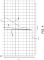
- FIG. 4 illustrates a graph 400 depicting a transient response of an operational amplifier with the slew-rate boost circuitry discussed herein and a transient response of an operational amplifier without the slew-rate boost circuitry.
- the graph 400 depicts voltage on the y-axis and time on the x-axis.
- Line 401 depicts an input voltage that is provided to the operational amplifier. As shown in FIG. 4 , the input voltage has a step voltage that increases from a first voltage level 410 to a second voltage level 412.
- Line 403 depicts the output voltage of the operational amplifier with the slew rate boost circuitry. The line 403 depicts the positive voltage slope of the output voltage during the transient response.
- Line 405 depicts the output voltage of the operational amplifier without the slew rate boost circuitry. As shown in FIG. 4 , the slew rate is increased as compared to the operational amplifier without the slew rate boost circuitry.
- FIG. 5 illustrates a graph 500 depicting a transient response of an operational amplifier with the slew-rate boost circuitry discussed herein and a transient response of an operational amplifier without the slew-rate boost circuitry.
- the graph 500 depicts voltage on the y-axis and time on the x-axis.
- Line 501 depicts an input voltage that is provided to the operational amplifier. As shown in FIG. 5 , the input voltage has a step voltage that decreases from a second voltage level 512 to a first voltage level 510.
- Line 503 depicts the output voltage of the operational amplifier with the slew rate boost circuitry. The line 503 depicts the negative voltage slope of the output voltage during the transient response.
- Line 505 depicts the output voltage of the operational amplifier without the slew rate boost circuitry. As shown in FIG. 5 , the slew rate is increased as compared to the operational amplifier without the slew rate boost circuitry.
- FIGS. 6A through 6C illustrate various graphs depicting a positive voltage slope and currents provided by the slew-rate boost circuitry according to an aspect.
- the graph of FIG. 6A depicts voltage level on the y-axis and time on the x-axis.
- Line 601 depicts an input voltage that is provided to the operational amplifier. As shown in FIG. 6A , the input voltage has a step voltage that increases from a first voltage level 610 to a second voltage level 612.
- Line 603 depicts the output voltage of the operational amplifier with the slew rate boost circuitry. The line 603 depicts the positive voltage slope of the output voltage during the transient response.
- FIG. 6C depicts the current level on the y-axis and time on the x-axis.
- line 605 depicts the boost current provided by the second control circuitry 106 of FIG. 1 .
- the boost current provided by the second control circuitry 106 is zero or close to zero.
- lines 607 and 609 depict the boost currents provided by the first control circuitry 104 of FIG. 1 .
- the boost currents are from the first control circuitry (e.g., 104, 204) - one for each capacitor in FIG. 1 (e.g., capacitors 112, 114).
- the lines 609 and 607 represent the drain currents of transistor 250 and transistor 248 of FIG. 2 , respectively.
- FIGS. 7A through 7C illustrate various graphs depicting a positive voltage slope and currents provided by the slew-rate boost circuitry according to an aspect.
- the graph of FIG. 7A depicts voltage level on the y-axis and time on the x-axis.
- Line 701 depicts an input voltage that is provided to the operational amplifier. As shown in FIG. 7A , the input voltage has a step voltage that decreases from a second voltage level 712 to a first voltage level 710.
- Line 703 depicts the output voltage of the operational amplifier with the slew rate boost circuitry. The line 703 depicts the negative voltage slope of the output voltage during the transient response.
- FIG. 7C depicts the current level on the y-axis and time on the x-axis.
- lines 707 and 705 depict the boost currents provided by the second control circuitry 106 of FIG. 1 .
- the boost currents are from the second control circuitry (e.g., 106, 206) - one for each capacitor in FIG. 1 (e.g., capacitors 112, 114).
- the lines 705 and 707 represent the drain currents of transistor 350 and transistor 348 of FIG. 3 , respectively.
- line 709 depicts the boost current provided by the first control circuitry 104 of FIG. 1 .
- the boost current provided by the first control circuitry 104 is zero or close to zero.
- FIGS. 8A and 8B illustrate graphs depicting boost currents over increasing values of the voltage differential (V diff ) according to an aspect.
- the voltage differential is the voltage difference between the first input 101 of FIG. 1 and the second input 103 of FIG. 1 .
- lines 801 and 802 depict the boost currents provided by the second control circuitry 106 of FIG. 1 (and supplied to the capacitors 112, 114 of FIG. 1 ).
- the boost current e.g., a negative current
- V1 first voltage threshold
- the boost current provided by the second control circuitry 106 continues to remain at zero or substantially zero.
- lines 803 and 804 depict the boost currents provided by the first control circuitry 104 of FIG. 1 (and supplied to the capacitors 112, 114 of FIG. 1 ).
- V2 the boost current
- FIG. 9 illustrates a flowchart 900 depicting example operations of an operational amplifier with a slew-rate boost circuitry according to an aspect.
- the flowchart 900 is explained with reference to the circuit 100 of FIG. 1 , the operations may be implemented by any of the examples discussed herein.
- the flowchart 900 of FIG. 9 illustrates the operations in sequential order, it will be appreciated that this is merely an example, and that additional or alternative operations may be included. Further, operations of FIG. 9 and related operations may be executed in a different order than that shown, or in a parallel or overlapping fashion.
- Operation 902 includes detecting a first voltage differential between a first input 101 of a differential amplifier 108 and a second input 103 of the differential amplifier 108.
- the first voltage differential is a voltage difference between the first input 101 and the second input 103 that exceeds a first voltage threshold.
- Operation 904 includes applying, at an output of the differential amplifier 108, a first boost current to charge a capacitor (e.g., capacitor 112 and/or capacitor 114) during a first period of time in which an output voltage 116 increases from a first voltage level to a second voltage level.
- the first boost current is applied at the input of the output stage 110.
- operation 902 and operation 904 are executed by the first control circuitry 104.
- the first boost current is added to the existing current to increase the slew-rate (e.g., the positive voltage slope).
- operation 904 is executed only during a transient response of the operational amplifier 105.
- Operation 906 includes detecting a second voltage differential between the first input 101 and the second input 103.
- the second voltage differential is a voltage difference between the first input 101 and the second input 103 that exceeds a second voltage threshold.
- Operation 908 includes applying, at the output of the differential amplifier 108, a second boost current to charge the capacitor (e.g., capacitor 112 and/or capacitor 114) during a second period of time in which the output voltage 116 decreases from the second voltage level to the first voltage level.
- the second boost current is applied at the input of the output stage 110.
- operation 902 and operation 904 are executed by the second control circuitry 106.
- the second boost current is added to the existing current to increase the slew-rate (e.g., the negative voltage slope).
- operation 908 is executed only during a transient response of the operational amplifier 105.
- the operations include removing the first boost current in response to expiration of the first period of time.
- the removal of the first boost current may include controlling the first boost current to have a value of zero or substantially zero.
- the operations may include removing the second boost current in response to expiration of the second period of time.
- the removal of the first boost current may include controlling the first boost current to have a value of zero or substantially zero.
- the first boost current is not applied during the second period of time, and the second boost current is not applied during the first period of time.
- the slew-rate boost circuitry is configured to, in response to the output voltage achieving the target voltage level, remove the boost current.
- the slew-rate boost circuitry is connected to the first input and the second input.
- the differential amplifier includes a first output and a second output, the first output being connected to the output stage, the second output being connected to the output stage, the slew-rate boost circuitry being connected to the first output and the second output.
- the slew-rate boost circuitry includes a current mirror, where the current mirror includes a first transistor and a second transistor. The first transistor is connected to the first output and the second transistor is connected to the second output.
- the slew-rate boost circuitry includes a differential voltage detector configured to detect the voltage differential.
- the capacitor is connected in parallel with the output stage.
- the boost current is a first boost current.
- the slew-rate boost circuitry includes a first control circuitry configured to detect that the voltage differential between the first input and the second input exceeds a first voltage threshold, and apply, at the output of the differential amplifier, the first boost current to charge the capacitor during a first period of time in which the output voltage increases from a first voltage level to a second voltage level.
- the slew-rate boost circuitry includes a second control circuitry configured to detect that the voltage differential between the first input and the second input exceeds a second voltage threshold, and apply, at the output of the differential amplifier, a second boost current to charge the capacitor during a second period of time in which the output voltage decreases from the second voltage level to the first voltage level.
- the differential amplifier includes a first input and a second input, where the first control circuitry configured to detect a first voltage differential between the first input and the second input, where, in response to the first voltage differential being detected, the first control circuitry is configured to apply the first boost current.
- the second control circuitry is configured to detect a second voltage differential between the first input and the second input, wherein, in response to the second voltage differential being detected, the second control circuitry is configured to apply the second boost current.
- the first boost current is not applied during the second period of time, and the second boost current is not applied during the first period of time.
- the differential amplifier includes a first input and a second input, where the first control circuitry is connected to the first input and the second input, the second control circuitry being connected to the first input and the second input.
- the differential amplifier includes a first output and a second output, the first output being connected to the output stage, the second output being connected to the output stage, the first control circuitry being connected to the first output and the second output, the second control circuitry being connected to the first output and the second output.
- Each of the first control circuitry and the second control circuitry includes a current mirror, the current mirror including a first transistor and a second transistor, the first transistor being connected to the first output, the second transistor being connected to the second output.
- the first control circuitry includes a first differential voltage detector configured to detect the first voltage differential, the second control circuitry including a second differential voltage detector configured to detect the second voltage differential.
- the method may include removing the first boost current in response to expiration of the first period of time and removing the second boost current in response to expiration of the second period of time.
- the first boost current is not applied during the second period of time, and the second boost current is not applied during the first period of time.
- a circuit comprising: an operational amplifier including a differential amplifier, a capacitor, and an output stage, the differential amplifier including a first input and a second input, the output stage configured to generate an output voltage; and a slew-rate boost circuitry connected to the operational amplifier, the slew-rate boost circuitry is configured to: detect a voltage differential between the first input and the second input; and apply, at an output of the differential amplifier, a boost current to charge the capacitor during a period of time in which the output voltage increases or decreases to a target voltage level.
- Clause 3 The circuit of clause 1 or 2, wherein the slew-rate boost circuitry is connected to the first input and the second input.
- the slew-rate boost circuitry includes a current mirror, the current mirror including a first transistor and a second transistor, the first transistor being connected to the first output, the second transistor being connected to the second output.
- Clause 6 The circuit of any of clauses 1 to 5, wherein the slew-rate boost circuitry includes a differential voltage detector configured to detect the voltage differential.
- the boost current is a first boost current
- the slew-rate boost circuitry including a first control circuitry configured to: detect that the voltage differential between the first input and the second input exceeds a first voltage threshold; and apply, at the output of the differential amplifier, the first boost current to charge the capacitor during a first period of time in which the output voltage increases from a first voltage level to a second voltage level.
- the slew-rate boost circuitry includes a second control circuitry configured to: detect that the voltage differential between the first input and the second input exceeds a second voltage threshold; and apply, at the output of the differential amplifier, a second boost current to charge the capacitor during a second period of time in which the output voltage decreases from the second voltage level to the first voltage level.
- a circuit comprising: an operational amplifier including a differential amplifier, a capacitor, and an output stage, the output stage configured to generate an output voltage; a first control circuitry configured to apply, at an output of the differential amplifier, a first boost current to charge the capacitor during a first period of time in which the output voltage increases from a first voltage level to a second voltage level; and a second control circuitry configured to apply, at the output of the differential amplifier, a second boost current to charge the capacitor during a second period of time in which the output voltage decreases from the second voltage level to the first voltage level.
- Clause 11 The circuit of clause 10, wherein the differential amplifier includes a first input and a second input, the first control circuitry configured to detect a first voltage differential between the first input and the second input, wherein, in response to the first voltage differential being detected, the first control circuitry is configured to apply the first boost current.
- Clause 12 The circuit of clause 11, wherein the second control circuitry is configured to detect a second voltage differential between the first input and the second input, wherein, in response to the second voltage differential being detected, the second control circuitry is configured to apply the second boost current.
- Clause 13 The circuit of any of clauses 10 to 12, wherein the first boost current is not applied during the second period of time, and the second boost current is not applied during the first period of time.
- Clause 14 The circuit of any of clauses 10 to 13, wherein the differential amplifier includes a first input and a second input, the first control circuitry being connected to the first input and the second input, the second control circuitry being connected to the first input and the second input.
- each of the first control circuitry and the second control circuitry includes a current mirror, the current mirror including a first transistor and a second transistor, the first transistor being connected to the first output, the second transistor being connected to the second output.
- Clause 17 The circuit of clause 15, wherein the first control circuitry includes a first differential voltage detector configured to detect the first voltage differential, the second control circuitry including a second differential voltage detector configured to detect the second voltage differential.
- a method for increasing a slew-rate of an operational amplifier comprising: detecting a first voltage differential between a first input of a differential amplifier and a second input of the differential amplifier; applying, at an output of the differential amplifier, a first boost current to charge a capacitor during a first period of time in which an output voltage increases from a first voltage level to a second voltage level; detecting a second voltage differential between the first input and the second input; and applying, at the output of the differential amplifier, a second boost current to charge the capacitor during a second period of time in which the output voltage decreases from the second voltage level to the first voltage level.
- Clause 19 The method of clause 18, further comprising: removing the first boost current in response to expiration of the first period of time; and removing the second boost current in response to expiration of the second period of time.
- Clause 20 The method of clause 18 or 19, wherein the first boost current is not applied during the second period of time, and the second boost current is not applied during the first period of time.
- Various implementations of the systems and techniques described here can be realized in digital electronic circuitry, integrated circuitry, specially designed ASICs (application specific integrated circuits), computer hardware, firmware, software, and/or combinations thereof. These various implementations can include implementation in one or more computer programs that are executable and/or interpretable on a programmable system including at least one programmable processor, which may be special or general purpose, coupled to receive data and instructions from, and to transmit data and instructions to, a storage system, at least one input device, and at least one output device.
- Various implementations of the systems and techniques described here can be realized as and/or generally be referred to herein as a circuit, a module, a block, or a system that can combine software and hardware aspects.
- a module may include the functions/acts/computer program instructions executing on a processor (e.g., a processor formed on a silicon substrate, a GaAs substrate, and the like) or some other programmable data processing apparatus.
- Methods discussed above may be implemented by hardware, software, firmware, middleware, microcode, hardware description languages, or any combination thereof.
- the program code or code segments to perform the necessary tasks may be stored in a machine or computer readable medium such as a storage medium.
- a processor(s) may perform the necessary tasks.
- a singular form may, unless definitely indicating a particular case in terms of the context, include a plural form.
- Spatially relative terms e.g., over, above, upper, under, beneath, below, lower, and so forth
- the relative terms above and below can, respectively, include vertically above and vertically below.
- the term adjacent can include laterally adjacent to or horizontally adjacent to.
- references to acts and symbolic representations of operations that may be implemented as program modules or functional processes include routines, programs, objects, components, data structures, etc., that perform particular tasks or implement particular abstract data types and may be described and/or implemented using existing hardware at existing structural elements.
- Such existing hardware may include one or more Central Processing Units (CPUs), digital signal processors (DSPs), application-specific-integrated-circuits, field programmable gate arrays (FPGAs) computers or the like.
- CPUs Central Processing Units
- DSPs digital signal processors
- FPGAs field programmable gate arrays
Landscapes
- Engineering & Computer Science (AREA)
- Power Engineering (AREA)
- Physics & Mathematics (AREA)
- Nonlinear Science (AREA)
- Amplifiers (AREA)
Abstract
Description
- Slew-rate may be the measure of how fast an operational amplifier can charge the output capacitance. A high value for the slew-rate may increase the performance of the operational amplifier but can also increase power consumption and/or affect other performance parameters such as bandwidth and noise.
- In some examples, the techniques described herein relate to a circuit including an operational amplifier that includes a differential amplifier, a capacitor, and an output stage. The differential amplifier includes a first input and a second input. The output stage is configured to generate an output voltage. The circuit includes a slew-rate boost circuitry connected to the operational amplifier. The slew-rate boost circuitry is configured to detect a voltage differential between the first input and the second input and apply, at an output of the differential amplifier, a boost current to charge the capacitor during a period of time in which the output voltage increases or decreases to a target voltage level.
- In some examples, the techniques described herein relate to a circuit including an operational amplifier that includes a differential amplifier, a capacitor, and an output stage. The output stage configured to generate an output voltage, a first control circuitry configured to apply, at an output of the differential amplifier, a first boost current to charge the capacitor during a first period of time in which the output voltage increases from a first voltage level to a second voltage level, and a second control circuitry configured to apply, at the output of the differential amplifier, a second boost current to charge the capacitor during a second period of time in which the output voltage decreases from the second voltage level to the first voltage level.
- In some examples, the techniques described herein relate to a method for increasing a slew-rate of an operational amplifier, the method including detecting a first voltage differential between a first input of a differential amplifier and a second input of the differential amplifier, applying, at an output of the differential amplifier, a first boost current to charge a capacitor during a first period of time in which an output voltage increases from a first voltage level to a second voltage level, detecting a second voltage differential between the first input and the second input, and applying, at the output of the differential amplifier, a second boost current to charge the capacitor during a second period of time in which the output voltage decreases from the second voltage level to the first voltage level.
-
-
FIG. 1 illustrates a circuit having an operational amplifier and slew-rate boost circuitry according to an aspect. -
FIG. 2 illustrates a first control circuitry of the slew-rate boost circuitry according to an aspect. -
FIG. 3 illustrates a second control circuitry of the slew-rate boost circuitry according to an aspect. -
FIG. 4 illustrates a slew rate of a positive voltage slope according to an aspect. -
FIG. 5 illustrates a slew rate of a negative voltage slope according to an aspect. -
FIGS. 6A through 6C illustrate graphs depicting voltage and boost current over time according to an aspect. -
FIGS. 7A through 7C illustrate graphs depicting voltage and boost current over time according to another aspect. -
FIGS. 8A and 8B illustrate graphs depicting boost current over increasing values of voltage differential according to an aspect. -
FIG. 9 illustrates a flowchart depicting example operations of an operational amplifier with a slew-rate boost circuitry according to an aspect. - This description relates to a slew-rate boost circuitry configured to increase a current applied to an operational amplifier during a slew condition, thereby reducing the amount of time to charge an output voltage of the operational amplifier to a target voltage level. For example, the slew-rate boost circuitry is configured to add a boost current to increase the slew-rate during the transient response of the operational amplifier. The operational amplifier may include a differential amplifier, an output stage coupled to an output of the differential amplifier, and one or more output capacitances coupled to the output of the differential amplifier or the output stage.
- The slew-rate boost circuitry includes a first control circuitry and a second control circuitry. The first control circuitry is configured to apply a first boost current to increase a positive voltage slope (e.g., a rising edge slope), and the second control circuitry 106 is configured to apply a second boost current to increase a negative voltage slope (e.g., a falling edge slope). Since the slew-rate boost circuitry independently monitors and controls the positive voltage slope and the negative voltage slope (e.g., via the first control circuitry and the second control circuitry), the response time of the operational amplifier can be improved while minimizing the effect on other parameters such as noise and bandwidth.
- In some examples, the first control circuitry is connected to the output of the differential amplifier. The first control circuitry is configured to apply, at the output of the differential amplifier, the first boost current to charge the output capacitance(s) during the slewing operation (e.g., during the period of time in which the output voltage increases from a first voltage level to a second voltage level). The first boost current may increase the positive voltage slope (e.g., the slew-rate) such that the output capacitance(s) are charged faster. When the output voltage reaches the second voltage level, the first control circuitry may remove the first boost current (e.g., provide a first boost current of zero or substantially zero). In other words, the first boost current may be applied during the transient response of the operational amplifier. Since the first boost current is applied during the transient response, the quiescent current may be minimized. For example, a slew-rate value may be proportional (e.g., directly proportional) to the quiescent current of a circuit that includes an operational amplifier. However, according to the techniques discussed herein, the slew-rate boost circuitry may increase the slew-rate while minimizing the quiescent current in the operational amplifier.
- In some examples, the second control circuitry is connected to the output of the differential amplifier. The second control circuitry is configured to apply, at the output of the differential amplifier, the second boost current to charge the output capacitance(s) during the slewing operation (e.g., during the period of time in which the output voltage decreases from the second voltage level to the first voltage level). The second boost current may increase the negative voltage slope (e.g., the slew-rate) such that the output capacitance(s) are charged faster. When the output voltage reaches the first voltage level, the second control circuitry may remove the second boost current (e.g., provide a second boost current of zero or substantially zero). In other words, the second boost current may be applied during the transient response of the operational amplifier. Similar to the first boost current, since the second boost current is applied during the transient response, the quiescent current may be minimized in the operational amplifier.
-
FIG. 1 illustrates acircuit 100 for increasing the slew-rate of anoperational amplifier 105 according to an aspect. The slew-rate may be the measure of how fast theoperational amplifier 105 can charge output capacitances (e.g.,capacitor 112, capacitor 114). Thecircuit 100 may apply a boost current to increase the rate at which the output capacitances are charged, where the boost current is applied when theoperational amplifier 105 is active. Theoperational amplifier 105 may be active when theoutput voltage 116 is changing in response to a change to the input voltage. In other words, theoperational amplifier 105 may be active during a transient response of the operational amplifier 105 (e.g., during a slewing operation). Thecircuit 100 may remove the boost current when theoperational amplifier 105 is not active (e.g., in a steady-state mode). Theoperational amplifier 105 may be in a non-active state when an equilibrium between the input and the output is achieved (e.g., no further voltage movements). Because thecircuit 100 may selectively apply the boost current during (e.g., only during) the transient response of theoperational amplifier 105, the quiescent current (IQ) of thecircuit 100 may be reduced, which can reduce power consumption. Furthermore, the boost current may be applied at an output of adifferential amplifier 108 or anoutput stage 110 of theoperational amplifier 105, which can reduce noise and/or distortion within thecircuit 100. - The
circuit 100 may be used in a wide variety of devices such as analog-to-digital converters (ADCs), digital-to-analog converters (DACs), buffers, or regulated power supplies. Theoperational amplifier 105 includes adifferential amplifier 108, anoutput stage 110, acapacitor 112, and acapacitor 114. - The
differential amplifier 108 includes afirst input 101 and asecond input 103. Thedifferential amplifier 108 is configured to amplify the voltage difference between thefirst input 101 and thesecond input 103. In some examples, thefirst input 101 is an inverting input. In some examples, thesecond input 103 is a non-inverting input. A voltage differential between thefirst input 101 and thesecond input 103 may represent an input signal. Theoutput stage 110 is connected to thedifferential amplifier 108. Theoutput stage 110 is configured to generate the output voltage 116 (e.g., the output of theoutput stage 110 is the output voltage 116). Theoutput stage 110 may include one or more electrical components such as transistor(s), amplifier(s), and/or voltage/current source(s). The topology of theoutput stage 110 may widely vary depending on the implementation of thecircuit 100. - In some examples, the
differential amplifier 108 includes afirst output 121 and asecond output 123. Similar to thefirst input 101 and thesecond input 103, thefirst output 121 and thesecond output 123 are differential. In some examples, thedifferential amplifier 108 is referred to as fully differential. In some examples, thefirst output 121 is a positive output. In some examples, thesecond output 123 is a negative output. The output voltages of thedifferential amplifier 108 may be equal but opposite in polarity. Thefirst output 121 is connected to the input of theoutput stage 110. Thesecond output 123 is connected to the input of theoutput stage 110. - The
capacitor 112 and thecapacitor 114 may be the output capacitances. Thecapacitor 112 and thecapacitor 114 may represent compensation and/or parasitic capacitances. In some examples, thecapacitor 112 is connected in parallel with theoutput stage 110. Thecapacitor 112 has a first terminal connected to the input of theoutput stage 110 and a second terminal connected to the output of theoutput stage 110. The first terminal of thecapacitor 112 may be also connected to thefirst output 121. In some examples, thecapacitor 114 is connected in parallel with theoutput stage 110. Thecapacitor 114 has a first terminal connected to the input of theoutput stage 110 and a second terminal connected to the output of theoutput stage 110. The first terminal of thecapacitor 112 may be also connected to thesecond output 123. - The
operational amplifier 105 may receive an input voltage and generate anoutput voltage 116 that corresponds to the input voltage. For example, if the input voltage changes from a threshold voltage (e.g., a first voltage level such as zero volts) to a higher voltage level (e.g., a second voltage level such as five volts), theoperational amplifier 105 increases theoutput voltage 116 from the first voltage level to the second voltage level and the slew-rate is the time to change theoutput voltage 116 from the first voltage level to the second voltage level (e.g., rising edge slope). Similarly, if the input voltage changes from the second voltage level to the first voltage level, theoperational amplifier 105 decreases theoutput voltage 116 from the second voltage level to the first voltage level and the slew-rate is the time to change theoutput voltage 116 from the second voltage level to the first voltage level (e.g., falling edge slope). - In further detail, if the voltage differential between the
first input 101 and thesecond input 103 exceeds a first threshold level, theoperational amplifier 105 converts theoutput voltage 116 from the first voltage level to the second voltage level (e.g., rising edge slope), which may be referred to as the transient response of theoperational amplifier 105. Similarly, if the voltage differential between thefirst input 101 and thesecond input 103 exceeds a second threshold level, theoperational amplifier 105 converts theoutput voltage 116 from the second voltage level to the first voltage level (e.g., falling edge slope), which may also be referred to as the transient response of theoperational amplifier 105. In some examples, the second threshold level is the same as the first threshold level. In some examples, the second threshold level is different from the first threshold level. - The
circuit 100 includes slew-rate boost circuitry 102 configured to add a boost current to increase the slew-rate during the transient response of theoperational amplifier 105. In some examples, the design of the slew-rate boost circuitry 102 is relatively small, which occupies a relatively small space in a converter, thereby reducing or eliminating compensation capacitors. Also, the slew-rate boost circuitry 102 can be used for low voltage or high voltage operational amplifiers. Further, the slew-rate boost circuitry 102 may increase the slew-rate of theoperational amplifier 105 without significantly increasing the overall quiescent current. The slew-rate boost circuitry 102 may be used with any type of operational amplifier topology. - The slew-
rate boost circuitry 102 includes afirst control circuitry 104 and a second control circuitry 106. Thefirst control circuitry 104 is configured to apply a boost current to increase the positive voltage slope (e.g., rising edge slope), and the second control circuitry 106 is configured to apply a boost current to increase the negative voltage slope (e.g., falling edge slope). In some examples, the positive voltage slope may be a first slew-rate and the negative voltage slope may be a second slew-rate. Also, since the slew-rate boost circuitry 102 independently monitors and controls the positive and negative voltage slopes (e.g., via thefirst control circuitry 104 and the second control circuitry 106), the response time of theoperational amplifier 105 can be improved while minimizing the effect on other parameters such as noise and bandwidth. - The
first control circuitry 104 is connected to thefirst input 101 and thesecond input 103 of thedifferential amplifier 108. Thefirst control circuitry 104 is configured to measure the voltage differential between thefirst input 101 and thesecond input 103 and detect a slewing condition, e.g., whether the voltage differential between thefirst input 101 and thesecond input 103 exceeds a threshold level. In some examples, thefirst control circuitry 104 detects whether the voltage differential is positive (e.g., increasing), and, in some examples, greater than a first voltage threshold. Thefirst control circuitry 104 may be connected to the output of thedifferential amplifier 108. Thefirst control circuitry 104 may be connected to the input of theoutput stage 110. In some examples, thefirst control circuitry 104 is connected to thefirst output 121 of thedifferential amplifier 108 and connected to thesecond output 123 of thedifferential amplifier 108. In some examples, thefirst control circuitry 104 is connected to anode 109, where thenode 109 is connected to thefirst output 121 and the input of theoutput stage 110. In some examples, thefirst control circuitry 104 is connected to anode 111, where thenode 111 is connected to thefirst output 121 and the input of theoutput stage 110. - The
first control circuitry 104 is configured to apply, at the output of thedifferential amplifier 108, a boost current (e.g., a first boost current) to charge the output capacitances (e.g., thecapacitor 112 and/or the capacitor 114) during the slewing operation (e.g., during the period of time in which the output voltage increases to the second voltage level). The boost current may increase the positive voltage slope (e.g., the slew-rate) such that the output capacitances are charged faster. When theoutput voltage 116 reaches the second voltage level, thefirst control circuitry 104 may remove the boost current. In other words, the boost current may be applied during the transient response of theoperational amplifier 105. - The second control circuitry 106 is connected to the
first input 101 and thesecond input 103 of thedifferential amplifier 108. The second control circuitry 106 is configured to measure the voltage differential between thefirst input 101 and thesecond input 103 and detect a slewing condition, e.g., whether the voltage differential between thefirst input 101 and thesecond input 103 exceeds a second voltage threshold. In some examples, the second control circuitry 106 is configured to detect whether the voltage differential is negative (e.g., decreasing) and, in some examples, greater than the second voltage threshold. The second control circuitry 106 may be connected to the output of thedifferential amplifier 108. The second control circuitry 106 may be connected to the input of theoutput stage 110. In some examples, the second control circuitry 106 is connected to thefirst output 121 of thedifferential amplifier 108 and connected to thesecond output 123 of thedifferential amplifier 108. In some examples, the second control circuitry 106 is connected to anode 109, where thenode 109 is connected to thefirst output 121 and the input of theoutput stage 110. In some examples, the second control circuitry 106 is connected to anode 111, where thenode 111 is connected to thefirst output 121 and the input of theoutput stage 110. - The second control circuitry 106 is configured to apply, at the output of the
differential amplifier 108, a boost current (e.g., a second boost current) to charge the output capacitances (e.g., thecapacitor 112 and/or the capacitor 114) during the slewing operation (e.g., during the period of time in which the output voltage decreases to the first voltage level). The boost current may increase the negative voltage slope such that the output capacitances are charged faster. When theoutput voltage 116 reaches the first voltage level, the second control circuitry 106 may remove the boost current. In other words, the boost current may be applied during the transient response of theoperational amplifier 105. -
FIG. 2 illustrates an example of afirst control circuitry 204 according to an aspect. Thefirst control circuitry 204 may be an example of thefirst control circuitry 104 ofFIG. 1 and may include any of the details discussed with that figure. - The
first control circuitry 204 includes adifferential voltage detector 220, asense amplifier 236, and acurrent mirror 251. Thecurrent mirror 251 is configured to generate the boost current, which is provided to thenode 109 ofFIG. 1 and thenode 111 ofFIG. 1 . - The
differential voltage detector 220 is configured to detect the voltage differential between thefirst input 101 ofFIG. 1 and thesecond input 103 ofFIG. 1 and determine a slewing condition, e.g., whether the voltage differential between thefirst input 101 ofFIG. 1 and thesecond input 103 ofFIG. 1 is positive, and, in some examples, exceeds a first voltage threshold. Thedifferential voltage detector 220 includes atransistor 226, atransistor 228, aresistor 230, aresistor 232, aresistor 222, aresistor 224, and a voltage source VDD. In some examples, the voltage source VDD is included in thefirst control circuitry 204. In some examples, the voltage source VDD is an external source voltage (e.g., a voltage that is received by the first control circuitry 204). In some examples, the voltage source VDD is a positive supply voltage. In some examples, thetransistor 226 includes a N-type transistor. In some examples, thetransistor 228 includes a N-type transistor. - The gate of the
transistor 226 is connected to thefirst input 101 ofFIG. 1 , the drain of thetransistor 226 is connected to a first terminal of theresistor 222, and the source of thetransistor 226 is connected to thesense amplifier 236. The gate of thetransistor 228 is connected to thesecond input 103 ofFIG. 1 , the drain of thetransistor 228 is connected to a first terminal of theresistor 224, and the source of thetransistor 228 is connected to thesense amplifier 236. Also, the source of thetransistor 226 is connected to a first terminal of theresistor 230, and the source of thetransistor 228 is connected to a first terminal of theresistor 232. A second terminal of theresistor 230 is connected to a second terminal of theresistor 232. Thetransistor 226, thetransistor 228, theresistor 230, and theresistor 232 are used for reading the differential voltage and to determine a slewing event. During a slewing event, imbalanced currents through thetransistor 226 and thetransistor 228 indicate an imbalance between the voltage drop across theresistor 230 and the resistor 232.x - The
sense amplifier 236 is configured to detect the voltage difference. Thesense amplifier 236 includes atransistor 238, atransistor 240, atransistor 241, acurrent source 242, and acurrent source 244. In some examples, thetransistor 238 is a P-type transistor. In some examples, thetransistor 240 is a P-type transistor. In some examples, thetransistor 241 is a P-type transistor. The source of thetransistor 238 is connected to the source oftransistor 228, the drain of thetransistor 238 is connected to thecurrent source 244, and the gate of thetransistor 238 is connected to the gate of thetransistor 240. Also, the drain of thetransistor 238 is connected to the gate of thetransistor 238. Also, the source of thetransistor 238 is connected to the source of thetransistor 241. The source of thetransistor 240 is connected to the source of thetransistor 226, the drain of thetransistor 240 is connected to thecurrent source 242, and the gate of thetransistor 240 is connected to the gate of thetransistor 238. Also, the drain of thetransistor 240 is connected to the gate of thetransistor 241. The source of thetransistor 241 is connected to the source of thetransistor 228, the drain of thetransistor 241 is connected to a drain of atransistor 246, and the gate of thetransistor 241 is connected to the drain of thetransistor 240. - The
first control circuitry 204 includes acurrent source 234. Thecurrent source 234 is connected to anode 231 disposed between theresistor 230 and theresistor 232. Thecurrent source 234 is also connected to a supply voltage VSS. The supply voltage VSS is connected to thecurrent source 242 and thecurrent source 244. Thefirst control circuitry 204 includes atransistor 246. In some examples, thetransistor 246 is an N-type transistor. The drain of thetransistor 246 is connected to the drain of thetransistor 241, the source of thetransistor 246 is connected to the supply voltage VSS, and the gate of thetransistor 246 is connected to the drain of thetransistor 246 and the gates oftransistor 248 and thetransistor 250. - The inputs of the
sense amplifier 236 are the sources of thetransistor 240 and thetransistor 238 and are connected to the sources of thetransistor 226 and thetransistor 228. The output of thesense amplifier 236 is the source of thetransistor 241 and is connected to one of the inputs of thesense amplifier 236, so that a negative feedback loop is created. To assure the stability of the negative feedback loop, source inputs and source output are used. - The current generated through the
transistor 241 is mirrored by thecurrent mirror 251 and provided to thenode 109 and thenode 111 ofFIG. 1 . For example, the output of thecurrent mirror 251 is the boost current that is provided to thenode 109 and thenode 111 ofFIG. 1 . Thecurrent mirror 251 includes atransistor 248 and atransistor 250. In some examples,transistor 248 is a N-type transistor. In some examples, thetransistor 250 is a N-type transistor. The drain of thetransistor 248 is connected to thenode 109, the source of thetransistor 248 is connected to the supply voltage VSS, and the gate of thetransistor 248 is connected to the gates of thetransistor 246 and thetransistor 250, as well as the drain of thetransistor 241. The drain of thetransistor 250 is connected to thenode 111 ofFIG. 1 , the source of thetransistor 250 is connected to the supply voltage VSS, and the gate of thetransistor 250 is connected to the gates of thetransistor 246 and thetransistor 248, as well as the drain of thetransistor 241. - In some examples, the
first control circuitry 204 may embed hysteresis at one or more locations in thefirst control circuitry 204. By embedding hysteresis in thefirst control circuitry 204, thefirst control circuitry 204 may be activated for controlled differential voltages (e.g., Vdiff >100mV). In some examples, the values forcurrent source 242 and thecurrent source 244 are different (e.g., mismatched) in order to create hysteresis. In some examples, hysteresis can be created by using different values for thetransistor 238 and thetransistor 240 or different values for theresistor 230 and theresistor 232. It is noted that the purpose of the hysteresis may be to activate thefirst control circuitry 204 in the event of relatively high differential voltage steps and to reduce the activation caused by noise or small signals. -
FIG. 3 illustrates an example of asecond control circuitry 306 according to an aspect. Thesecond control circuitry 306 may be an example of the second control circuitry 106 ofFIG. 1 and may include any of the details discussed with that figure. - The
second control circuitry 306 includes adifferential voltage detector 320, asense amplifier 336, and acurrent mirror 351. Thecurrent mirror 351 is configured to generate the boost current, which is provided to thenode 109 ofFIG. 1 and thenode 111 ofFIG. 1 . - The
differential voltage detector 320 is configured to detect the voltage differential between thefirst input 101 ofFIG. 1 and thesecond input 103 ofFIG. 1 and determine a slewing condition, e.g., whether the voltage differential between thefirst input 101 ofFIG. 1 and thesecond input 103 ofFIG. 1 is negative and exceeds a threshold level. Thedifferential voltage detector 220 includes atransistor 326, atransistor 328, aresistor 330, aresistor 332, aresistor 322, aresistor 324, and a voltage source VDD. In some examples, thetransistor 326 includes a P-type transistor. In some examples, thetransistor 328 includes a P-type transistor. - The gate of the
transistor 326 is connected to thefirst input 101 ofFIG. 1 , the drain of thetransistor 326 is connected to a first terminal of theresistor 322, and the source of thetransistor 326 is connected to thesense amplifier 336. The gate of thetransistor 328 is connected to thesecond input 103 ofFIG. 1 , the drain of thetransistor 328 is connected to a first terminal of theresistor 324, and the source of thetransistor 328 is connected to thesense amplifier 336. Also, the source of thetransistor 326 is connected to a first terminal of theresistor 330, and the source of thetransistor 326 is connected to a first terminal of theresistor 332. A second terminal of theresistor 330 is connected to a second terminal of theresistor 332. Thetransistor 326, thetransistor 328, theresistor 330, and theresistor 332 are used for reading the differential voltage and to determine a slewing event. During a slewing event, imbalanced currents through thetransistor 326 and thetransistor 328 indicate an imbalance between the voltage drop across theresistor 330 and theresistor 332. - The
sense amplifier 336 is configured to detect the voltage difference. Thesense amplifier 336 includes atransistor 338, atransistor 340, atransistor 341, acurrent source 342, and acurrent source 344. In some examples, thetransistor 338 is a N-type transistor. In some examples, thetransistor 340 is a N-type transistor. In some examples, thetransistor 341 is a N-type transistor. The source of thetransistor 338 is connected to the source oftransistor 328, the drain of thetransistor 338 is connected to thecurrent source 344, and the gate of thetransistor 338 is connected to the gate of thetransistor 340. Also, the drain of thetransistor 338 is connected to the gate of thetransistor 338. Also, the source of thetransistor 338 is connected to the source of thetransistor 341. The source of thetransistor 340 is connected to the source of thetransistor 326, the drain of thetransistor 340 is connected to thecurrent source 342, and the gate of thetransistor 340 is connected to the gate of thetransistor 338. Also, the drain of thetransistor 340 is connected to the gate of thetransistor 341. The source of thetransistor 341 is connected to the source of thetransistor 328, the drain of thetransistor 341 is connected to a drain of atransistor 346, and the gate of thetransistor 341 is connected to the drain of thetransistor 340. - The
second control circuitry 306 includes acurrent source 334. Thecurrent source 334 is connected to anode 331 disposed between theresistor 330 and theresistor 332. Thecurrent source 334 is also connected to a supply voltage VSS. The supply voltage VSS is connected to thecurrent source 342 and thecurrent source 344. Thesecond control circuitry 306 includes atransistor 346. In some examples, thetransistor 346 is a P-type transistor. The drain of thetransistor 346 is connected to the drain of thetransistor 341, the source of thetransistor 346 is connected to the supply voltage VDD, and the gate of thetransistor 346 is connected to the drain of thetransistor 346 and the gates oftransistor 348 and thetransistor 350. - The inputs of the
sense amplifier 336 are the sources of thetransistor 340 and thetransistor 338 and are connected to the sources of thetransistor 326 and thetransistor 328. The output of thesense amplifier 336 is the source of thetransistor 341 and is connected to one of the inputs of thesense amplifier 336, so that a negative feedback loop is created. To assure the stability of the negative feedback loop, source inputs and source output are used. - The current generated through the
transistor 341 is mirrored by thecurrent mirror 351 and provided to thenode 109 and thenode 111 ofFIG. 1 . For example, the output of thecurrent mirror 351 is the boost current that is provided to thenode 109 and thenode 111 ofFIG. 1 . Thecurrent mirror 351 includes atransistor 348 and atransistor 350. In some examples,transistor 348 is a P-type transistor. In some examples, thetransistor 350 is a P-type transistor. The drain of thetransistor 348 is connected to thenode 109, the source of thetransistor 348 is connected to the supply voltage VSS, and the gate of thetransistor 348 is connected to the gates of thetransistor 346 and thetransistor 350, as well as the drain of thetransistor 341. The drain of thetransistor 350 is connected to thenode 111 ofFIG. 1 , the source of thetransistor 350 is connected to the supply voltage VSS, and the gate of thetransistor 350 is connected to the gates of thetransistor 346 and thetransistor 348, as well as the drain of thetransistor 341. - In some examples, the
second control circuitry 306 may embed hysteresis at one or more locations in thesecond control circuitry 306. By embedding hysteresis in thesecond control circuitry 306, thesecond control circuitry 306 may be activated for controlled differential voltages (e.g., Vdiff >100mV). In some examples, the values forcurrent source 342 and thecurrent source 344 are different (e.g., mismatched) in order to create hysteresis. In some examples, hysteresis can be created by using different values for thetransistor 338 and thetransistor 340 or different values for theresistor 330 and theresistor 332. It is noted that the purpose of the hysteresis may be to activate thesecond control circuitry 306 in the event of relatively high differential voltage steps and to reduce the activation caused by noise or small signals. -
FIG. 4 illustrates agraph 400 depicting a transient response of an operational amplifier with the slew-rate boost circuitry discussed herein and a transient response of an operational amplifier without the slew-rate boost circuitry. Thegraph 400 depicts voltage on the y-axis and time on the x-axis. Line 401 depicts an input voltage that is provided to the operational amplifier. As shown inFIG. 4 , the input voltage has a step voltage that increases from afirst voltage level 410 to asecond voltage level 412.Line 403 depicts the output voltage of the operational amplifier with the slew rate boost circuitry. Theline 403 depicts the positive voltage slope of the output voltage during the transient response.Line 405 depicts the output voltage of the operational amplifier without the slew rate boost circuitry. As shown inFIG. 4 , the slew rate is increased as compared to the operational amplifier without the slew rate boost circuitry. -
FIG. 5 illustrates agraph 500 depicting a transient response of an operational amplifier with the slew-rate boost circuitry discussed herein and a transient response of an operational amplifier without the slew-rate boost circuitry. Thegraph 500 depicts voltage on the y-axis and time on the x-axis. Line 501 depicts an input voltage that is provided to the operational amplifier. As shown inFIG. 5 , the input voltage has a step voltage that decreases from asecond voltage level 512 to afirst voltage level 510.Line 503 depicts the output voltage of the operational amplifier with the slew rate boost circuitry. Theline 503 depicts the negative voltage slope of the output voltage during the transient response.Line 505 depicts the output voltage of the operational amplifier without the slew rate boost circuitry. As shown inFIG. 5 , the slew rate is increased as compared to the operational amplifier without the slew rate boost circuitry. -
FIGS. 6A through 6C illustrate various graphs depicting a positive voltage slope and currents provided by the slew-rate boost circuitry according to an aspect. The graph ofFIG. 6A depicts voltage level on the y-axis and time on the x-axis. Line 601 depicts an input voltage that is provided to the operational amplifier. As shown inFIG. 6A , the input voltage has a step voltage that increases from afirst voltage level 610 to asecond voltage level 612.Line 603 depicts the output voltage of the operational amplifier with the slew rate boost circuitry. Theline 603 depicts the positive voltage slope of the output voltage during the transient response. The graph ofFIG. 6B and the graph ofFIG. 6C depicts the current level on the y-axis and time on the x-axis. InFIG. 6B ,line 605 depicts the boost current provided by the second control circuitry 106 ofFIG. 1 . For the rising edge, since the second control circuitry 106 is not activated, the boost current provided by the second control circuitry 106 is zero or close to zero. InFIG. 6C ,lines first control circuitry 104 ofFIG. 1 . In some examples, the boost currents are from the first control circuitry (e.g., 104, 204) - one for each capacitor inFIG. 1 (e.g.,capacitors 112, 114). In some examples, thelines transistor 250 andtransistor 248 ofFIG. 2 , respectively. -
FIGS. 7A through 7C illustrate various graphs depicting a positive voltage slope and currents provided by the slew-rate boost circuitry according to an aspect. The graph ofFIG. 7A depicts voltage level on the y-axis and time on the x-axis.Line 701 depicts an input voltage that is provided to the operational amplifier. As shown inFIG. 7A , the input voltage has a step voltage that decreases from asecond voltage level 712 to afirst voltage level 710.Line 703 depicts the output voltage of the operational amplifier with the slew rate boost circuitry. Theline 703 depicts the negative voltage slope of the output voltage during the transient response. The graph ofFIG. 7B and the graph ofFIG. 7C depicts the current level on the y-axis and time on the x-axis. InFIG. 7B ,lines FIG. 1 . In some examples, the boost currents are from the second control circuitry (e.g., 106, 206) - one for each capacitor inFIG. 1 (e.g.,capacitors 112, 114). In some examples, thelines transistor 350 andtransistor 348 ofFIG. 3 , respectively. InFIG. 7C ,line 709 depicts the boost current provided by thefirst control circuitry 104 ofFIG. 1 . For the falling edge, since thefirst control circuitry 104 is not activated, the boost current provided by thefirst control circuitry 104 is zero or close to zero. -
FIGS. 8A and 8B illustrate graphs depicting boost currents over increasing values of the voltage differential (Vdiff) according to an aspect. The voltage differential is the voltage difference between thefirst input 101 ofFIG. 1 and thesecond input 103 ofFIG. 1 . InFIG. 8A ,lines FIG. 1 (and supplied to thecapacitors FIG. 1 ). As shown inFIG. 8A , the boost current (e.g., a negative current) increases when a voltage differential is detected and the boost current decreases until the voltage differential reaches a first voltage threshold (V1) at which the boost current is zero or substantially zero. As the voltage differential continues to increase to a second voltage threshold (V2), the boost current provided by the second control circuitry 106 continues to remain at zero or substantially zero. InFIG. 8B ,lines first control circuitry 104 ofFIG. 1 (and supplied to thecapacitors FIG. 1 ). As shown inFIG. 8B , when the voltage differential reaches the second voltage threshold (V2), the boost current increases. -
FIG. 9 illustrates aflowchart 900 depicting example operations of an operational amplifier with a slew-rate boost circuitry according to an aspect. Although theflowchart 900 is explained with reference to thecircuit 100 ofFIG. 1 , the operations may be implemented by any of the examples discussed herein. Although theflowchart 900 ofFIG. 9 illustrates the operations in sequential order, it will be appreciated that this is merely an example, and that additional or alternative operations may be included. Further, operations ofFIG. 9 and related operations may be executed in a different order than that shown, or in a parallel or overlapping fashion. -
Operation 902 includes detecting a first voltage differential between afirst input 101 of adifferential amplifier 108 and asecond input 103 of thedifferential amplifier 108. In some examples, the first voltage differential is a voltage difference between thefirst input 101 and thesecond input 103 that exceeds a first voltage threshold.Operation 904 includes applying, at an output of thedifferential amplifier 108, a first boost current to charge a capacitor (e.g.,capacitor 112 and/or capacitor 114) during a first period of time in which anoutput voltage 116 increases from a first voltage level to a second voltage level. In some examples, the first boost current is applied at the input of theoutput stage 110. In some examples,operation 902 andoperation 904 are executed by thefirst control circuitry 104. In some examples, the first boost current is added to the existing current to increase the slew-rate (e.g., the positive voltage slope). In some examples,operation 904 is executed only during a transient response of theoperational amplifier 105. -
Operation 906 includes detecting a second voltage differential between thefirst input 101 and thesecond input 103. In some examples, the second voltage differential is a voltage difference between thefirst input 101 and thesecond input 103 that exceeds a second voltage threshold.Operation 908 includes applying, at the output of thedifferential amplifier 108, a second boost current to charge the capacitor (e.g.,capacitor 112 and/or capacitor 114) during a second period of time in which theoutput voltage 116 decreases from the second voltage level to the first voltage level. In some examples, the second boost current is applied at the input of theoutput stage 110. In some examples,operation 902 andoperation 904 are executed by the second control circuitry 106. In some examples, the second boost current is added to the existing current to increase the slew-rate (e.g., the negative voltage slope). In some examples,operation 908 is executed only during a transient response of theoperational amplifier 105. - In some examples, the operations include removing the first boost current in response to expiration of the first period of time. In some examples, the removal of the first boost current may include controlling the first boost current to have a value of zero or substantially zero. The operations may include removing the second boost current in response to expiration of the second period of time. In some examples, the removal of the first boost current may include controlling the first boost current to have a value of zero or substantially zero. In some examples, the first boost current is not applied during the second period of time, and the second boost current is not applied during the first period of time.
- The slew-rate boost circuitry is configured to, in response to the output voltage achieving the target voltage level, remove the boost current. The slew-rate boost circuitry is connected to the first input and the second input. The differential amplifier includes a first output and a second output, the first output being connected to the output stage, the second output being connected to the output stage, the slew-rate boost circuitry being connected to the first output and the second output. The slew-rate boost circuitry includes a current mirror, where the current mirror includes a first transistor and a second transistor. The first transistor is connected to the first output and the second transistor is connected to the second output. The slew-rate boost circuitry includes a differential voltage detector configured to detect the voltage differential. The capacitor is connected in parallel with the output stage. The boost current is a first boost current. The slew-rate boost circuitry includes a first control circuitry configured to detect that the voltage differential between the first input and the second input exceeds a first voltage threshold, and apply, at the output of the differential amplifier, the first boost current to charge the capacitor during a first period of time in which the output voltage increases from a first voltage level to a second voltage level. The slew-rate boost circuitry includes a second control circuitry configured to detect that the voltage differential between the first input and the second input exceeds a second voltage threshold, and apply, at the output of the differential amplifier, a second boost current to charge the capacitor during a second period of time in which the output voltage decreases from the second voltage level to the first voltage level.
- The differential amplifier includes a first input and a second input, where the first control circuitry configured to detect a first voltage differential between the first input and the second input, where, in response to the first voltage differential being detected, the first control circuitry is configured to apply the first boost current. The second control circuitry is configured to detect a second voltage differential between the first input and the second input, wherein, in response to the second voltage differential being detected, the second control circuitry is configured to apply the second boost current. The first boost current is not applied during the second period of time, and the second boost current is not applied during the first period of time. The differential amplifier includes a first input and a second input, where the first control circuitry is connected to the first input and the second input, the second control circuitry being connected to the first input and the second input. The differential amplifier includes a first output and a second output, the first output being connected to the output stage, the second output being connected to the output stage, the first control circuitry being connected to the first output and the second output, the second control circuitry being connected to the first output and the second output. Each of the first control circuitry and the second control circuitry includes a current mirror, the current mirror including a first transistor and a second transistor, the first transistor being connected to the first output, the second transistor being connected to the second output. The first control circuitry includes a first differential voltage detector configured to detect the first voltage differential, the second control circuitry including a second differential voltage detector configured to detect the second voltage differential.
- The method may include removing the first boost current in response to expiration of the first period of time and removing the second boost current in response to expiration of the second period of time. The first boost current is not applied during the second period of time, and the second boost current is not applied during the first period of time.
- Clause 1. A circuit comprising: an operational amplifier including a differential amplifier, a capacitor, and an output stage, the differential amplifier including a first input and a second input, the output stage configured to generate an output voltage; and a slew-rate boost circuitry connected to the operational amplifier, the slew-rate boost circuitry is configured to: detect a voltage differential between the first input and the second input; and apply, at an output of the differential amplifier, a boost current to charge the capacitor during a period of time in which the output voltage increases or decreases to a target voltage level.
- Clause 2. The circuit of clause 1, wherein the slew-rate boost circuitry is configured to: in response to the output voltage achieving the target voltage level, remove the boost current.
- Clause 3. The circuit of clause 1 or 2, wherein the slew-rate boost circuitry is connected to the first input and the second input.
- Clause 4. The circuit of any of clauses 1 to 3, wherein the differential amplifier includes a first output and a second output, the first output being connected to the output stage, the second output being connected to the output stage, the slew-rate boost circuitry being connected to the first output and the second output.
- Clause 5. The circuit of clause 4, wherein the slew-rate boost circuitry includes a current mirror, the current mirror including a first transistor and a second transistor, the first transistor being connected to the first output, the second transistor being connected to the second output.
- Clause 6. The circuit of any of clauses 1 to 5, wherein the slew-rate boost circuitry includes a differential voltage detector configured to detect the voltage differential.
- Clause 7. The circuit of any of clauses 1 to 6, wherein the capacitor is connected in parallel with the output stage.
- Clause 8. The circuit of any of clauses 1 to 7, wherein the boost current is a first boost current, the slew-rate boost circuitry including a first control circuitry configured to: detect that the voltage differential between the first input and the second input exceeds a first voltage threshold; and apply, at the output of the differential amplifier, the first boost current to charge the capacitor during a first period of time in which the output voltage increases from a first voltage level to a second voltage level.
- Clause 9. The circuit of clause 8, wherein the slew-rate boost circuitry includes a second control circuitry configured to: detect that the voltage differential between the first input and the second input exceeds a second voltage threshold; and apply, at the output of the differential amplifier, a second boost current to charge the capacitor during a second period of time in which the output voltage decreases from the second voltage level to the first voltage level.
- Clause 10. A circuit comprising: an operational amplifier including a differential amplifier, a capacitor, and an output stage, the output stage configured to generate an output voltage; a first control circuitry configured to apply, at an output of the differential amplifier, a first boost current to charge the capacitor during a first period of time in which the output voltage increases from a first voltage level to a second voltage level; and a second control circuitry configured to apply, at the output of the differential amplifier, a second boost current to charge the capacitor during a second period of time in which the output voltage decreases from the second voltage level to the first voltage level.
- Clause 11. The circuit of clause 10, wherein the differential amplifier includes a first input and a second input, the first control circuitry configured to detect a first voltage differential between the first input and the second input, wherein, in response to the first voltage differential being detected, the first control circuitry is configured to apply the first boost current.
- Clause 12. The circuit of clause 11, wherein the second control circuitry is configured to detect a second voltage differential between the first input and the second input, wherein, in response to the second voltage differential being detected, the second control circuitry is configured to apply the second boost current.
- Clause 13. The circuit of any of clauses 10 to 12, wherein the first boost current is not applied during the second period of time, and the second boost current is not applied during the first period of time.
- Clause 14. The circuit of any of clauses 10 to 13, wherein the differential amplifier includes a first input and a second input, the first control circuitry being connected to the first input and the second input, the second control circuitry being connected to the first input and the second input.
- Clause 15. The circuit of any of clauses 10 to 14, wherein the differential amplifier includes a first output and a second output, the first output being connected to the output stage, the second output being connected to the output stage, the first control circuitry being connected to the first output and the second output, the second control circuitry being connected to the first output and the second output.
- Clause 16. The circuit of clause 15, wherein each of the first control circuitry and the second control circuitry includes a current mirror, the current mirror including a first transistor and a second transistor, the first transistor being connected to the first output, the second transistor being connected to the second output.
- Clause 17. The circuit of clause 15, wherein the first control circuitry includes a first differential voltage detector configured to detect the first voltage differential, the second control circuitry including a second differential voltage detector configured to detect the second voltage differential.
- Clause 18. A method for increasing a slew-rate of an operational amplifier, the method comprising: detecting a first voltage differential between a first input of a differential amplifier and a second input of the differential amplifier; applying, at an output of the differential amplifier, a first boost current to charge a capacitor during a first period of time in which an output voltage increases from a first voltage level to a second voltage level; detecting a second voltage differential between the first input and the second input; and applying, at the output of the differential amplifier, a second boost current to charge the capacitor during a second period of time in which the output voltage decreases from the second voltage level to the first voltage level.
- Clause 19. The method of clause 18, further comprising: removing the first boost current in response to expiration of the first period of time; and removing the second boost current in response to expiration of the second period of time.
- Clause 20. The method of clause 18 or 19, wherein the first boost current is not applied during the second period of time, and the second boost current is not applied during the first period of time.
- Various implementations of the systems and techniques described here can be realized in digital electronic circuitry, integrated circuitry, specially designed ASICs (application specific integrated circuits), computer hardware, firmware, software, and/or combinations thereof. These various implementations can include implementation in one or more computer programs that are executable and/or interpretable on a programmable system including at least one programmable processor, which may be special or general purpose, coupled to receive data and instructions from, and to transmit data and instructions to, a storage system, at least one input device, and at least one output device. Various implementations of the systems and techniques described here can be realized as and/or generally be referred to herein as a circuit, a module, a block, or a system that can combine software and hardware aspects. For example, a module may include the functions/acts/computer program instructions executing on a processor (e.g., a processor formed on a silicon substrate, a GaAs substrate, and the like) or some other programmable data processing apparatus.
- Some of the above examples are described as processes or methods depicted as flowcharts. Although the flowcharts describe the operations as sequential processes, many of the operations may be performed in parallel, concurrently or simultaneously. In addition, the order of operations may be re-arranged. The processes may be terminated when their operations are completed but may also have additional steps not included in the figure. The processes may correspond to methods, functions, procedures, subroutines, subprograms, etc.
- Methods discussed above, some of which are illustrated by the flow charts, may be implemented by hardware, software, firmware, middleware, microcode, hardware description languages, or any combination thereof. When implemented in software, firmware, middleware or microcode, the program code or code segments to perform the necessary tasks may be stored in a machine or computer readable medium such as a storage medium. A processor(s) may perform the necessary tasks.
- It will be understood that, although the terms first, second, etc. may be used herein to describe various elements, these elements should not be limited by these terms. These terms are only used to distinguish one element from another. For example, a first element could be termed a second element, and, similarly, a second element could be termed a first element, without departing from the scope of examples discussed herein. As used herein, the term and/or includes any and all combinations of one or more of the associated listed items.
- It will be understood that, in the foregoing description, when an element is referred to as being on, connected to, electrically connected to, coupled to, or electrically coupled to another element, it may be directly on, connected or coupled to the other element, or one or more intervening elements may be present. In contrast, when an element is referred to as being directly on, directly connected to or directly coupled to another element, there are no intervening elements present. Although the terms directly on, directly connected to, or directly coupled to may not be used throughout the detailed description, elements that are shown as being directly on, directly connected or directly coupled can be referred to as such. The claims of the application, if any, may be amended to recite exemplary relationships described in the specification or shown in the figures.
- As used in this specification, a singular form may, unless definitely indicating a particular case in terms of the context, include a plural form. Spatially relative terms (e.g., over, above, upper, under, beneath, below, lower, and so forth) are intended to encompass different orientations of the device in use or operation in addition to the orientation depicted in the figures. In some implementations, the relative terms above and below can, respectively, include vertically above and vertically below. In some implementations, the term adjacent can include laterally adjacent to or horizontally adjacent to.
- While certain features of the described implementations have been illustrated as described herein, many modifications, substitutions, changes and equivalents will now occur to those skilled in the art. It is, therefore, to be understood that the appended claims are intended to cover all such modifications and changes as fall within the scope of the implementations. It should be understood that they have been presented by way of example only, not limitation, and various changes in form and details may be made. Any portion of the apparatus and/or methods described herein may be combined in any combination, except mutually exclusive combinations. The implementations described herein can include various combinations and/or sub-combinations of the functions, components and/or features of the different implementations described.
- Unless otherwise defined, all terms (including technical and scientific terms) used herein have the same meaning as commonly understood by one of ordinary skill in the art to which example embodiments belong. It will be further understood that terms, e.g., those defined in commonly used dictionaries, should be interpreted as having a meaning that is consistent with their meaning in the context of the relevant art and will not be interpreted in an idealized or overly formal sense unless expressly so defined herein.
- Portions of the above example embodiments and corresponding detailed description are presented in terms of software, or algorithms and symbolic representations of operation on data bits within a computer memory. These descriptions and representations are the ones by which those of ordinary skill in the art effectively convey the substance of their work to others of ordinary skill in the art. An algorithm, as the term is used here, and as it is used generally, is conceived to be a self-consistent sequence of steps leading to a desired result. The steps are those requiring physical manipulations of physical quantities. Usually, though not necessarily, these quantities take the form of optical, electrical, or magnetic signals capable of being stored, transferred, combined, compared, and otherwise manipulated. It has proven convenient at times, principally for reasons of common usage, to refer to these signals as bits, values, elements, symbols, characters, terms, numbers, or the like.
- In the above illustrative embodiments, reference to acts and symbolic representations of operations (e.g., in the form of flowcharts) that may be implemented as program modules or functional processes include routines, programs, objects, components, data structures, etc., that perform particular tasks or implement particular abstract data types and may be described and/or implemented using existing hardware at existing structural elements. Such existing hardware may include one or more Central Processing Units (CPUs), digital signal processors (DSPs), application-specific-integrated-circuits, field programmable gate arrays (FPGAs) computers or the like.
- It should be borne in mind, however, that all of these and similar terms are to be associated with the appropriate physical quantities and are merely convenient labels applied to these quantities. Unless specifically stated otherwise, or as is apparent from the discussion, terms such as processing or computing or calculating or determining of displaying or the like, refer to the action and processes of a computer system, or similar electronic computing device, that manipulates and transforms data represented as physical, electronic quantities within the computer system's registers and memories into other data similarly represented as physical quantities within the computer system memories or registers or other such information storage, transmission or display devices.
- Lastly, it should also be noted that whilst the accompanying claims set out particular combinations of features described herein, the scope of the present disclosure is not limited to the particular combinations hereafter claimed, but instead extends to encompass any combination of features or embodiments herein disclosed irrespective of whether or not that particular combination has been specifically enumerated in the accompanying claims at this time.
Claims (15)
- A circuit comprising:an operational amplifier including a differential amplifier, a capacitor, and an output stage, the differential amplifier including a first input and a second input, the output stage configured to generate an output voltage; anda slew-rate boost circuitry connected to the operational amplifier, the slew-rate boost circuitry is configured to:detect a voltage differential between the first input and the second input; andapply, at an output of the differential amplifier, a boost current to charge the capacitor during a period of time in which the output voltage increases or decreases to a target voltage level.
- The circuit of claim 1, wherein the slew-rate boost circuitry is configured to:
in response to the output voltage achieving the target voltage level, remove the boost current. - The circuit of claim 1 or 2, wherein the slew-rate boost circuitry is connected to the first input and the second input.
- The circuit of any of claims 1 to 3, wherein the differential amplifier includes a first output and a second output, the first output being connected to the output stage, the second output being connected to the output stage, the slew-rate boost circuitry being connected to the first output and the second output.
- The circuit of claim 4, wherein the slew-rate boost circuitry includes a current mirror, the current mirror including a first transistor and a second transistor, the first transistor being connected to the first output, the second transistor being connected to the second output.
- The circuit of any of claims 1 to 5, wherein the slew-rate boost circuitry includes a differential voltage detector configured to detect the voltage differential.
- The circuit of any of claims 1 to 6, wherein the capacitor is connected in parallel with the output stage.
- The circuit of any of claims 1 to 7, wherein the boost current is a first boost current, the slew-rate boost circuitry including a first control circuitry configured to:detect that the voltage differential between the first input and the second input exceeds a first voltage threshold; andapply, at the output of the differential amplifier, the first boost current to charge the capacitor during a first period of time in which the output voltage increases from a first voltage level to a second voltage level.
- The circuit of claim 8, wherein the slew-rate boost circuitry includes a second control circuitry configured to:detect that the voltage differential between the first input and the second input exceeds a second voltage threshold; andapply, at the output of the differential amplifier, a second boost current to charge the capacitor during a second period of time in which the output voltage decreases from the second voltage level to the first voltage level.
- The circuit of claim 9, wherein the first boost current is not applied during the second period of time, and the second boost current is not applied during the first period of time.
- The circuit of claim 9, wherein the differential amplifier includes a first output and a second output, the first output being connected to the output stage, the second output being connected to the output stage, the first control circuitry being connected to the first output and the second output, the second control circuitry being connected to the first output and the second output.
- The circuit of claim 9, wherein each of the first control circuitry and the second control circuitry includes a current mirror, the current mirror including a first transistor and a second transistor, the first transistor being connected to the first output, the second transistor being connected to the second output.
- A method for increasing a slew-rate of an operational amplifier, the method comprising:detecting a first voltage differential between a first input of a differential amplifier and a second input of the differential amplifier;applying, at an output of the differential amplifier, a first boost current to charge a capacitor during a first period of time in which an output voltage increases from a first voltage level to a second voltage level;detecting a second voltage differential between the first input and the second input; andapplying, at the output of the differential amplifier, a second boost current to charge the capacitor during a second period of time in which the output voltage decreases from the second voltage level to the first voltage level.
- The method of claim 13, further comprising:removing the first boost current in response to expiration of the first period of time; andremoving the second boost current in response to expiration of the second period of time.
- The method of claim 13 or 14, wherein the first boost current is not applied during the second period of time, and the second boost current is not applied during the first period of time.
Applications Claiming Priority (1)
| Application Number | Priority Date | Filing Date | Title |
|---|---|---|---|
| US17/931,947 US12597896B2 (en) | 2022-09-14 | 2022-09-14 | Slew-rate boost circuitry |
Publications (1)
| Publication Number | Publication Date |
|---|---|
| EP4350989A1 true EP4350989A1 (en) | 2024-04-10 |
Family
ID=87695810
Family Applications (1)
| Application Number | Title | Priority Date | Filing Date |
|---|---|---|---|
| EP23191905.1A Pending EP4350989A1 (en) | 2022-09-14 | 2023-08-17 | Slew-rate boost circuitry |
Country Status (4)
| Country | Link |
|---|---|
| US (1) | US12597896B2 (en) |
| EP (1) | EP4350989A1 (en) |
| CN (1) | CN117713697A (en) |
| TW (1) | TW202416655A (en) |
Citations (3)
| Publication number | Priority date | Publication date | Assignee | Title |
|---|---|---|---|---|
| US5317281A (en) * | 1993-01-12 | 1994-05-31 | Raytheon Company | Slew rate booster circuit |
| US20050285676A1 (en) * | 2004-06-28 | 2005-12-29 | Jones Mark A | Slew rate enhancement circuitry for folded cascode amplifier |
| US7362173B1 (en) * | 2005-09-16 | 2008-04-22 | National Semiconductor Corporation | System and method for providing slew rate enhancement for two stage CMOS amplifiers |
Family Cites Families (1)
| Publication number | Priority date | Publication date | Assignee | Title |
|---|---|---|---|---|
| US6437645B1 (en) | 2001-02-15 | 2002-08-20 | Texas Instruments Incorporated | Slew rate boost circuitry and method |
-
2022
- 2022-09-14 US US17/931,947 patent/US12597896B2/en active Active
-
2023
- 2023-08-17 EP EP23191905.1A patent/EP4350989A1/en active Pending
- 2023-08-25 TW TW112132021A patent/TW202416655A/en unknown
- 2023-09-13 CN CN202311180368.6A patent/CN117713697A/en active Pending
Patent Citations (3)
| Publication number | Priority date | Publication date | Assignee | Title |
|---|---|---|---|---|
| US5317281A (en) * | 1993-01-12 | 1994-05-31 | Raytheon Company | Slew rate booster circuit |
| US20050285676A1 (en) * | 2004-06-28 | 2005-12-29 | Jones Mark A | Slew rate enhancement circuitry for folded cascode amplifier |
| US7362173B1 (en) * | 2005-09-16 | 2008-04-22 | National Semiconductor Corporation | System and method for providing slew rate enhancement for two stage CMOS amplifiers |
Also Published As
| Publication number | Publication date |
|---|---|
| TW202416655A (en) | 2024-04-16 |
| US20240088853A1 (en) | 2024-03-14 |
| US12597896B2 (en) | 2026-04-07 |
| CN117713697A (en) | 2024-03-15 |
Similar Documents
| Publication | Publication Date | Title |
|---|---|---|
| EP3208942B1 (en) | Input device | |
| EP2894537A1 (en) | Voltage regulator | |
| US12026115B2 (en) | Compensating DC loss in USB 2.0 high speed applications | |
| US20050033998A1 (en) | Power supply circuit and semiconductor integrated circuit device | |
| US20150002218A1 (en) | Device and method for compensating for voltage drops | |
| US11569807B2 (en) | Voltage comparator circuit, power management circuit, electronic device | |
| US9665113B2 (en) | High-speed multiphase precision clamping circuit | |
| US9363070B2 (en) | Low power squelch circuit | |
| US12597896B2 (en) | Slew-rate boost circuitry | |
| US20240171175A1 (en) | Redriver and resistive termination unit for a redriver | |
| US12174063B2 (en) | Sampling circuit, optical detection system, display apparatus and sampling method | |
| CN113726337B (en) | Current compensation circuit and operation method of compensation current | |
| US11128260B2 (en) | Trans impedance amplifier capacitance isolation stage | |
| US10579083B1 (en) | Managing linear regulator transient voltages upon sleep transitions | |
| US11973507B2 (en) | Comparator circuit | |
| US10497455B2 (en) | Apparatus for sampling electrical signals with reduced leakage current and associated methods | |
| JP3319732B2 (en) | Voltage control circuit, network device, and voltage detection method | |
| EP4624939A1 (en) | Differential current sensor | |
| US10862470B2 (en) | Comparator circuitry | |
| CN113447697A (en) | Signal detection circuit, signal detection method, touch panel and display device | |
| US7893729B2 (en) | Voltage/current conversion circuit | |
| JP2021535649A (en) | Power amplifier with tracking power supply | |
| US12249909B2 (en) | Power supply noise reduction by current cancellation circuit | |
| CN112152653B (en) | Circuit with multiple receivers | |
| US20240028061A1 (en) | Feedback control system and feedback control method |
Legal Events
| Date | Code | Title | Description |
|---|---|---|---|
| PUAI | Public reference made under article 153(3) epc to a published international application that has entered the european phase |
Free format text: ORIGINAL CODE: 0009012 |
|
| STAA | Information on the status of an ep patent application or granted ep patent |
Free format text: STATUS: THE APPLICATION HAS BEEN PUBLISHED |
|
| AK | Designated contracting states |
Kind code of ref document: A1 Designated state(s): AL AT BE BG CH CY CZ DE DK EE ES FI FR GB GR HR HU IE IS IT LI LT LU LV MC ME MK MT NL NO PL PT RO RS SE SI SK SM TR |
|
| P01 | Opt-out of the competence of the unified patent court (upc) registered |
Effective date: 20240416 |
|
| STAA | Information on the status of an ep patent application or granted ep patent |
Free format text: STATUS: REQUEST FOR EXAMINATION WAS MADE |
|
| 17P | Request for examination filed |
Effective date: 20241010 |
|
| RBV | Designated contracting states (corrected) |
Designated state(s): AL AT BE BG CH CY CZ DE DK EE ES FI FR GB GR HR HU IE IS IT LI LT LU LV MC ME MK MT NL NO PL PT RO RS SE SI SK SM TR |
|
| STAA | Information on the status of an ep patent application or granted ep patent |
Free format text: STATUS: EXAMINATION IS IN PROGRESS |
|
| 17Q | First examination report despatched |
Effective date: 20250217 |