EP4350931A1 - A charge pump control system - Google Patents
A charge pump control system Download PDFInfo
- Publication number
- EP4350931A1 EP4350931A1 EP22306492.4A EP22306492A EP4350931A1 EP 4350931 A1 EP4350931 A1 EP 4350931A1 EP 22306492 A EP22306492 A EP 22306492A EP 4350931 A1 EP4350931 A1 EP 4350931A1
- Authority
- EP
- European Patent Office
- Prior art keywords
- charge pump
- balancing
- switch
- cell
- control system
- Prior art date
- Legal status (The legal status is an assumption and is not a legal conclusion. Google has not performed a legal analysis and makes no representation as to the accuracy of the status listed.)
- Pending
Links
Images


Classifications
-
- H—ELECTRICITY
- H02—GENERATION; CONVERSION OR DISTRIBUTION OF ELECTRIC POWER
- H02J—ELECTRIC POWER NETWORKS; CIRCUIT ARRANGEMENTS OR SYSTEMS FOR SUPPLYING OR DISTRIBUTING ELECTRIC POWER; SYSTEMS FOR STORING ELECTRIC ENERGY
- H02J7/00—Circuit arrangements for charging or discharging batteries or for supplying loads from batteries
- H02J7/50—Circuit arrangements for charging or discharging batteries or for supplying loads from batteries acting upon multiple batteries simultaneously or sequentially
- H02J7/52—Circuit arrangements for charging or discharging batteries or for supplying loads from batteries acting upon multiple batteries simultaneously or sequentially for charge balancing, e.g. equalisation of charge between batteries
-
- H—ELECTRICITY
- H02—GENERATION; CONVERSION OR DISTRIBUTION OF ELECTRIC POWER
- H02J—ELECTRIC POWER NETWORKS; CIRCUIT ARRANGEMENTS OR SYSTEMS FOR SUPPLYING OR DISTRIBUTING ELECTRIC POWER; SYSTEMS FOR STORING ELECTRIC ENERGY
- H02J7/00—Circuit arrangements for charging or discharging batteries or for supplying loads from batteries
- H02J7/50—Circuit arrangements for charging or discharging batteries or for supplying loads from batteries acting upon multiple batteries simultaneously or sequentially
- H02J7/52—Circuit arrangements for charging or discharging batteries or for supplying loads from batteries acting upon multiple batteries simultaneously or sequentially for charge balancing, e.g. equalisation of charge between batteries
- H02J7/54—Passive balancing, e.g. using resistors or parallel MOSFETs
-
- H—ELECTRICITY
- H02—GENERATION; CONVERSION OR DISTRIBUTION OF ELECTRIC POWER
- H02J—ELECTRIC POWER NETWORKS; CIRCUIT ARRANGEMENTS OR SYSTEMS FOR SUPPLYING OR DISTRIBUTING ELECTRIC POWER; SYSTEMS FOR STORING ELECTRIC ENERGY
- H02J7/00—Circuit arrangements for charging or discharging batteries or for supplying loads from batteries
- H02J7/50—Circuit arrangements for charging or discharging batteries or for supplying loads from batteries acting upon multiple batteries simultaneously or sequentially
- H02J7/52—Circuit arrangements for charging or discharging batteries or for supplying loads from batteries acting upon multiple batteries simultaneously or sequentially for charge balancing, e.g. equalisation of charge between batteries
- H02J7/56—Active balancing, e.g. using capacitor-based, inductor-based or DC-DC converters
-
- H—ELECTRICITY
- H02—GENERATION; CONVERSION OR DISTRIBUTION OF ELECTRIC POWER
- H02J—ELECTRIC POWER NETWORKS; CIRCUIT ARRANGEMENTS OR SYSTEMS FOR SUPPLYING OR DISTRIBUTING ELECTRIC POWER; SYSTEMS FOR STORING ELECTRIC ENERGY
- H02J7/00—Circuit arrangements for charging or discharging batteries or for supplying loads from batteries
- H02J7/90—Regulation of charging or discharging current or voltage
- H02J7/933—Regulation of charging or discharging current or voltage the cycle being controlled or terminated in response to electric parameters
-
- H—ELECTRICITY
- H02—GENERATION; CONVERSION OR DISTRIBUTION OF ELECTRIC POWER
- H02J—ELECTRIC POWER NETWORKS; CIRCUIT ARRANGEMENTS OR SYSTEMS FOR SUPPLYING OR DISTRIBUTING ELECTRIC POWER; SYSTEMS FOR STORING ELECTRIC ENERGY
- H02J7/00—Circuit arrangements for charging or discharging batteries or for supplying loads from batteries
- H02J7/90—Regulation of charging or discharging current or voltage
- H02J7/94—Regulation of charging or discharging current or voltage in response to battery current
-
- H—ELECTRICITY
- H02—GENERATION; CONVERSION OR DISTRIBUTION OF ELECTRIC POWER
- H02J—ELECTRIC POWER NETWORKS; CIRCUIT ARRANGEMENTS OR SYSTEMS FOR SUPPLYING OR DISTRIBUTING ELECTRIC POWER; SYSTEMS FOR STORING ELECTRIC ENERGY
- H02J7/00—Circuit arrangements for charging or discharging batteries or for supplying loads from batteries
- H02J7/90—Regulation of charging or discharging current or voltage
- H02J7/96—Regulation of charging or discharging current or voltage in response to battery voltage
-
- H—ELECTRICITY
- H02—GENERATION; CONVERSION OR DISTRIBUTION OF ELECTRIC POWER
- H02M—APPARATUS FOR CONVERSION BETWEEN AC AND AC, BETWEEN AC AND DC, OR BETWEEN DC AND DC, AND FOR USE WITH MAINS OR SIMILAR POWER SUPPLY SYSTEMS; CONVERSION OF DC OR AC INPUT POWER INTO SURGE OUTPUT POWER; CONTROL OR REGULATION THEREOF
- H02M1/00—Details of apparatus for conversion
- H02M1/14—Arrangements for reducing ripples from DC input or output
- H02M1/15—Arrangements for reducing ripples from DC input or output using active elements
-
- H—ELECTRICITY
- H02—GENERATION; CONVERSION OR DISTRIBUTION OF ELECTRIC POWER
- H02M—APPARATUS FOR CONVERSION BETWEEN AC AND AC, BETWEEN AC AND DC, OR BETWEEN DC AND DC, AND FOR USE WITH MAINS OR SIMILAR POWER SUPPLY SYSTEMS; CONVERSION OF DC OR AC INPUT POWER INTO SURGE OUTPUT POWER; CONTROL OR REGULATION THEREOF
- H02M3/00—Conversion of DC power input into DC power output
- H02M3/02—Conversion of DC power input into DC power output without intermediate conversion into AC
- H02M3/04—Conversion of DC power input into DC power output without intermediate conversion into AC by static converters
- H02M3/06—Conversion of DC power input into DC power output without intermediate conversion into AC by static converters using resistors or capacitors, e.g. potential divider
- H02M3/07—Conversion of DC power input into DC power output without intermediate conversion into AC by static converters using resistors or capacitors, e.g. potential divider using capacitors charged and discharged alternately by semiconductor devices with control electrode, e.g. charge pumps
-
- H—ELECTRICITY
- H01—ELECTRIC ELEMENTS
- H01M—PROCESSES OR MEANS, e.g. BATTERIES, FOR THE DIRECT CONVERSION OF CHEMICAL ENERGY INTO ELECTRICAL ENERGY
- H01M10/00—Secondary cells; Manufacture thereof
- H01M10/42—Methods or arrangements for servicing or maintenance of secondary cells or secondary half-cells
- H01M10/425—Structural combination with electronic components, e.g. electronic circuits integrated to the outside of the casing
- H01M2010/4271—Battery management systems including electronic circuits, e.g. control of current or voltage to keep battery in healthy state, cell balancing
Definitions
- the present disclosure relates to charge pump control systems, and in particular to charge pump control systems for battery management systems (BMSs).
- BMSs battery management systems
- the battery management system comprises:
- such a charge pump control system can reduce the consumption of the charge pump by changing the charge pump switching frequency while maintaining the charge pump output voltage ripple close to a specification, whatever the load.
- the charge pump control system comprises: a controller that is configured to set the switching frequency of the charge pump based on the number of switch drivers that are providing their respective cell-balancing-switches with a drive signal to close the cell-balancing-switch.
- the controller is configured to use a look-up table or database to determine the required switching frequency for a given number of switch drivers that are providing their respective cell-balancing-switches with a drive signal to close the cell-balancing-switch.
- the charge pump control system is configured to determine the amplitude of ripple in the output voltage that is provided by the charge pump and set the switching frequency of the charge pump based on the determined amplitude of the ripple.
- the charge pump control system is configured to:
- the charge pump control system is configured to provide the clock-adjustment-signal based on the level of ripple in the output voltage provided by the charge pump.
- the charge pump control system is configured to provide the clock-adjustment-signal by looking up a value for the clock-adjustment-signal in a look-up table based on the number of switch drivers that are providing their respective cell-balancing-switches with a drive signal to close the cell-balancing-switch.
- the charge pump control system is configured to modify the frequency of the clock-signal in order to provide the charge-pump-clock-signal by:
- the charge pump control system is configured to set the frequency of a charge-pump-clock-signal by: setting an operational parameter of a clock that provides a charge-pump-clock-signal based on the number of switch-drivers that are providing their respective cell-balancing-switches with a drive signal to close the cell-balancing-switch.
- the charge pump control system further comprises: a DC output voltage loop for setting the output voltage of the charge pump to a constant value by regulating the current through a flying capacitor in the charge pump.
- setting the switching frequency of the charge pump comprises using a look-up table or database to determine the required switching frequency for a given number of switch drivers that are providing their respective cell-balancing-switches with a drive signal to close the cell-balancing-switch.
- setting the switching frequency of the charge pump comprises:
- a charge pump can be used to supply drivers of cell balancing switches (one for each cell). In this case the current load of the charge pump depends on the number of cells balanced.
- BMS applications can require that the BMS consumption on the battery stack is as low as possible, especially in cyclic mode when the main source of consumption is the cell balancing.
- the charge pump can be optimized to supply the maximum number of drivers (current load / ripple / current consumption). If the charge pump is supplying fewer drivers (when fewer cells are balanced) than the maximum, then the charge pump is no longer optimized because the current load is smaller than its maximum capability. This causes unnecessary overconsumption.
- Examples that will be disclosed herein can improve performance of the charge pump in terms of current consumption, whatever number of cells are being supplied by the charge pump.
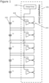
- FIG 1 illustrates a battery management system (BMS) 101, which in this example is implemented on an integrated circuit (IC).
- BMS 101 is shown connected to nine battery cells 102.
- the battery cells 102 are connected in series to provide a stack of battery cells.
- the BMS 101 includes a plurality of cell-balancing-switches 103, one for each of the plurality of battery cells 102. These cell-balancing-switches 103 can be implemented as PMOS MOSFETs in some examples. Each cell-balancing-switch 103 is in parallel with a respective one of the battery cells 102.
- the BMS 101 also includes a plurality of switch-drivers 104, one for each of the cell-balancing-switches 103. Each switch-driver 104 is for providing a drive signal to selectively close a respective one of the cell-balancing-switches 103.
- a cell balancing procedure can be applied in which each battery cell 102 can be discharged with the cell-balancing-switch 103.
- the BMS 101 also includes bleed resistors in parallel with each battery call 102 such that closing a cell-balancing-switch 103 does not short the battery call 102.
- bleed resistors are not shown in Figure 1 to simplify the illustration of the components of the BMS 101 that are key to the present disclosure.
- the BMS 101 also includes a charge pump 105 that is configured to provide an output voltage to each of the plurality of switch-drivers 104.
- the charge pump 105 senses the output voltage and adjusts a current source that charges a flying capacitor, as will be discussed in more detail with reference to Figure 5 .
- the charge pump 105 is operable at a switching frequency that sets the maximum output current.
- the switching frequency also has an impact on the level of ripple in the voltage at the output of the charge pump 105.
- the level of this ripple is constant for a static load, as is the case in the present application.
- the current consumption of the charge pump 105 is Ivbat_CP.
- Figure 2 shows a plot 207 of the level of ripple in the output voltage provided by the charge pump (on the vertical axis) versus the number of cells being balanced (on the horizontal axis) for a charge pump that is operated at a fixed switching frequency.
- the charge pump that is represented by the plot of Figure 2 is designed for the following requirements:
- Figure 3 shows: a plot 310 of the switching frequency of the charge pump (to illustrate that it is kept constant in this illustration); and a plot 311 of the level of ripple voltage in the output voltage provided by the charge pump, versus the number of cells being balanced (on the horizontal axis).
- Figure 4 shows another plot that illustrates that the current drawn on the charge pump (on the vertical axis) decreases as the number of cell balancing stages that are operating decreases.
- Examples of the present disclosure that will be described below can advantageously reduce the consumption of the charge pump by changing the charge pump switching frequency while maintaining the charge pump output voltage ripple close to the specification, whatever the load.
- Figure 5 shows a charge pump 505 for providing an output voltage 506 to each of a plurality of switch-drivers (not shown in Figure 5 ).
- a DC output voltage loop is provided for setting the output voltage 506 of the charge pump 505 to a constant value (or an almost constant value, in that it tends towards a predetermined value) by regulating the current through a flying capacitor in the charge pump.
- a DC control block 507 in Figure 5 which causes the current provided to the charge pump 505 by a variable current source 528 to increase, thereby implementing a regulation loop that causes the flying capacitor charge current to be increased.
- the charge pump 505 of Figure 5 is operated such that its DC output voltage is constant whatever the current drawn at its output by regulating its flying capacitor current charge.
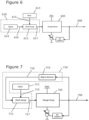
- Figure 6 shows a charge pump 605 for providing an output voltage 606 to each of a plurality of switch-drivers (not shown in Figure 6 ), along with a charge pump control system 618 according to an embodiment of the present disclosure.
- load configuration e.g. N_cells [0 to 9]
- x Iload_CB [0 to 270uA]
- the charge pump control system 618 includes a controller (specifically a digital controller 614 in this implementation) that is configured to set the switching frequency of the charge pump 605 based on the number of switch drivers that are providing their respective cell-balancing-switches with a drive signal to close the cell-balancing-switch.
- the switching frequency of the charge pump 605 is set by an open loop.
- the digital controller 614 can determine the number of cells that are to be balanced (for example: because the digital controller 614 provides the control signals to the switch-drivers to close the associated cell-balancing-switches; or because the digital controller 614 has access to computer memory that stores an identifier of the number of cells that are to be balanced), and can then set the switching frequency of the charge pump 605 in order to decrease the consumption of the charge pump 605 whilst still achieving an acceptable ripple voltage.
- the digital controller 614 can use a look-up table or database to determine the required switching frequency for a given number of cells that are being balanced.
- the switching / working frequencies that will be used for each load configuration can be set for a specific BMS at manufacture. That is, optimum switching frequencies for a given part and for a given N_cell system can slightly differ from part to part. Therefore, the optimum switching frequencies can be determined at the time of manufacture so that they can subsequently be used by the charge pump control system 618.
- the charge pump control system 618 receives a clock-signal 615 from a clock 613.
- the clock 613 may be part of the charge pump control system 618, it may be part of the BMS, or it may be provided as part of a different system.
- the charge pump control system 618 also includes a clock tuning block 612.
- the digital controller 614 of the charge pump control system 618 in this implementation provide a clock-adjustment-signal 616 based on the number of switch drivers that are providing their respective cell-balancing-switches with a drive signal to close the cell-balancing-switch. For example by using a look-up table as indicated above.
- the clock tuning block 612 modifies the frequency of the clock-signal 615 based on the clock-adjustment-signal 616 in order to provide a charge-pump-clock-signal 617.
- the clock tuning block 612 can modify the frequency of the clock-signal 615 in order to provide the charge-pump-clock-signal 617 by determining a frequency-factor based on the clock-adjustment-signal 616 and multiplying the clock-signal 615 by the frequency-factor.
- the clock tuning block 612 can be implemented as a simple frequency multiplier or divider.
- the charge pump control system 618 can then provide the charge-pump-clock-signal 617 to the charge pump 605 in order to set the switching frequency of the charge pump 605.
- the charge pump control system can set an operational parameter of a clock that (directly) provides a charge-pump-clock-signal based on the number of switch-drivers that are providing their respective cell-balancing-switches with a drive signal to close the cell-balancing-switch.
- the clock-signal that is directly provided by a clock can be adjusted, as opposed to modifying the (fixed) clock-signal that is provided by a clock as is the case in Figure 6 .
- Figure 7 shows a charge pump 705 for providing an output voltage 706 to each of a plurality of switch-drivers (not shown in Figure 7 ), along with a charge pump control system 718 according to another embodiment of the present disclosure.
- the charge pump control system 718 determines the amplitude of the ripple in the output voltage 706 that is provided by the charge pump 705 and set the switching frequency of the charge pump 705 based on the determined amplitude of the ripple.
- the charge pump control system 718 includes a ripple detector 719 and a clock tuning block 712.
- a clock 713 which provides a clock-signal 715 to the charge pump control system 718, is also shown in Figure 7 .
- the ripple detector 719 monitors the output voltage 706 that is provided by the charge pump 705.
- the ripple detector 719 provides a clock-adjustment-signal 716 at its output, which has a value that is proportional to the size of the ripple in the output voltage 706.
- This clock-adjustment-signal 716 (which can be considered as a feedback signal) is provided to the clock tuning block 712.
- the ripple detector 719 compares the size of the detected ripple voltage with at least two threshold values: a lower-threshold-value that represents a minimum acceptable value for the ripple voltage; and an upper-threshold-value that represents a maximum acceptable value for the ripple voltage. If the detected ripple voltage is not between the lower-threshold-value and the upper-threshold-value, then the ripple detector 719 sets the clock-adjustment-signal 716 such that the switching frequency of the charge pump 705 will either be increased or decreased such that the ripple voltage will move closer to it's acceptable range of values and ultimately to a value that is within the ripple amplitude range that is defined by the upper-threshold-value and the lower-threshold-value.
- the functionality of comparing the size of the detected ripple voltage with the at least two threshold values can be performed by the clock tuning block 712.
- the clock tuning block 712 provides a charge-pump-clock-signal 717 that has a frequency that is a function of a base clock (the clock-signal 715) combined with the feedback signal (the clock-adjustment-signal 716). Consequently, the frequency of the clock signal that supplies the charge pump 705 is tuned according to the feedback signal generated by the ripple detector 719. Therefore, a clock frequency control loop is provided by the example of Figure 7 .
- the charge pump control systems of Figure 6 and Figure 7 do not interfere with the DC output voltage loop that is described with reference to Figure 5 because the DC output voltage loop can be considered as a relatively fast loop that maintains the DC output voltage at a constant value.
- the charge pump control systems of Figure 6 and Figure 7 can be considered as implementing much slower control of the charge pump because the number of cells that are being balanced typically changes infrequently. For example, there could be anything from the order of minutes or hours between a change in the number of cells being balanced.
- This "slow loop" is that slow due to the particular load behaviour, so that it behaves more or less as a slow sequence of DC currents.
- the charge pump provides the output voltage (Vout) via the DC control loop that is described with reference to Figure 5 , at a frequency set point where the ripple voltage is an acceptable level due to the charge pump control system of Figure 6 or Figure 7 .
- the DC output voltage loop that is described with reference to Figure 5 can be considered part of any of the charge pump control systems that are described herein.
- Figure 8 shows plots 820, 821 of the operation of a charge pump that is controlled by the charge pump control system of Figures 6 or 7 .
- Figure 8 shows: a plot 821 of the switching frequency of the charge pump; and a plot 820 of the level of ripple voltage in the output voltage provided by the charge pump, versus the number of cells being balanced (on the horizontal axis).
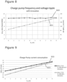
- Figure 9 shows a comparison between the current consumption of a charge pump that does not use a charge pump control system of Figures 6 or 7 , and one that does.
- a first plot 922 in Figure 9 shows current consumption of a charge pump that does not use a charge pump control system of Figures 6 or 7 .
- the first plot 922 is the same as the plot that is shown in Figure 4 .
- a second plot 923 in Figure 9 shows current consumption of a charge pump that does use a charge pump control system of Figures 6 or 7 . It can be seen from Figure 9 that the charge pump current consumption benefits from the decreased switching frequency that is enabled by the charge pump control system of Figures 6 and 7 .
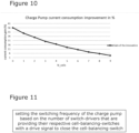
- Figure 10 shows a plot of the percentage improvements in charge pump current consumption that is achieved by using the charge pump control system of Figures 6 and 7 .
- FIG 11 illustrates schematically a method of controlling a charge pump control system for a BMS according to an embodiment of the present disclosure. Features of such a BMS are described in detail above.
- the method includes the step of setting the switching frequency of the charge pump based on the number of switch-drivers that are providing their respective cell-balancing-switches with a drive signal to close the cell-balancing-switch.
- controlling the charge pump in this way can advantageously improve the efficiency of the charge pump and reduce it's current consumption.
- Examples disclosed herein adapt the switching frequency of the charge pump.
- a predefined table of the switching frequency required for each number of balanced cells is used.
- a ripple detector is used to automatically adapt the switching frequency of the charge pump.
- a control loop is provided in some implementations that adapts the charge pump switching frequency according to the ripple observed at the charge pump output that supplies the cell balancing stages. Decreasing the charge pump frequency with the number of active cell balancing stages such as to maintain constant the charge pump output ripple results in significant savings to current consumption.
- Examples disclosed herein provide an improvement of the power consumption of a charge pump supplying cells balancing feature on BMS applications. Such examples can employ a strategy of adapting the frequency of the internal clock to fit the number of cells managed by the cells balancing feature.
- the set of instructions/method steps described above are implemented as functional and software instructions embodied as a set of executable instructions which are effected on a computer or machine which is programmed with and controlled by said executable instructions. Such instructions are loaded for execution on a processor (such as one or more CPUs).
- processor includes microprocessors, microcontrollers, processor modules or subsystems (including one or more microprocessors or microcontrollers), or other control or computing devices.
- a processor can refer to a single component or to plural components.
- the set of instructions/methods illustrated herein and data and instructions associated therewith are stored in respective storage devices, which are implemented as one or more non-transient machine or computer-readable or computer-usable storage media or mediums.
- Such computer-readable or computer usable storage medium or media is (are) considered to be part of an article (or article of manufacture).
- An article or article of manufacture can refer to any manufactured single component or multiple components.
- the non-transient machine or computer usable media or mediums as defined herein excludes signals, but such media or mediums may be capable of receiving and processing information from signals and/or other transient mediums.
- Example embodiments of the material discussed in this specification can be implemented in whole or in part through network, computer, or data based devices and/or services. These may include cloud, internet, intranet, mobile, desktop, processor, look-up table, microcontroller, consumer equipment, infrastructure, or other enabling devices and services. As may be used herein and in the claims, the following non-exclusive definitions are provided.
- one or more instructions or steps discussed herein are automated.
- the terms automated or automatically mean controlled operation of an apparatus, system, and/or process using computers and/or mechanical/electrical devices without the necessity of human intervention, observation, effort and/or decision.
- any components said to be coupled may be coupled or connected either directly or indirectly.
- additional components may be located between the two components that are said to be coupled.
Landscapes
- Engineering & Computer Science (AREA)
- Power Engineering (AREA)
- Dc-Dc Converters (AREA)
- Charge And Discharge Circuits For Batteries Or The Like (AREA)
Abstract
Description
- The present disclosure relates to charge pump control systems, and in particular to charge pump control systems for battery management systems (BMSs).
- According to a first aspect of the present disclosure there is provided a charge pump control system for a battery management system, wherein:
the battery management system comprises: - a plurality of cell-balancing-switches, one for each of a plurality of battery cells, wherein each cell-balancing-switch is in parallel with a respective one of the battery cells;
- a plurality of switch-drivers, one for each of the cell-balancing-switches, wherein each switch-driver is for providing a drive signal to selectively close a respective one of the cell-balancing-switches; and
- a charge pump that is configured to provide an output voltage to each of the plurality of switch-drivers, wherein the charge pump is operable at a switching frequency that sets the maximum output current;
- Advantageously, such a charge pump control system can reduce the consumption of the charge pump by changing the charge pump switching frequency while maintaining the charge pump output voltage ripple close to a specification, whatever the load.
- In one or more embodiments, the charge pump control system comprises:
a controller that is configured to set the switching frequency of the charge pump based on the number of switch drivers that are providing their respective cell-balancing-switches with a drive signal to close the cell-balancing-switch. - In one or more embodiments, the controller is configured to use a look-up table or database to determine the required switching frequency for a given number of switch drivers that are providing their respective cell-balancing-switches with a drive signal to close the cell-balancing-switch.
- In one or more embodiments, the charge pump control system is configured to determine the amplitude of ripple in the output voltage that is provided by the charge pump and set the switching frequency of the charge pump based on the determined amplitude of the ripple.
- In one or more embodiments, the charge pump control system is configured to:
- receive a clock-signal from a clock;
- provide a clock-adjustment-signal based on the number of switch drivers that are providing their respective cell-balancing-switches with a drive signal to close the cell-balancing-switch;
- modify the frequency of the clock-signal based on the clock-adjustment-signal in order to provide a charge-pump-clock-signal; and
- provide the charge-pump-clock-signal to the charge pump in order to set the switching frequency of the charge pump.
- In one or more embodiments, the charge pump control system is configured to provide the clock-adjustment-signal based on the level of ripple in the output voltage provided by the charge pump.
- In one or more embodiments, the charge pump control system is configured to provide the clock-adjustment-signal by looking up a value for the clock-adjustment-signal in a look-up table based on the number of switch drivers that are providing their respective cell-balancing-switches with a drive signal to close the cell-balancing-switch.
- In one or more embodiments, the charge pump control system is configured to modify the frequency of the clock-signal in order to provide the charge-pump-clock-signal by:
- determining a frequency-factor based on the clock-adjustment-signal; and
- multiplying the clock-signal by the frequency-factor.
- In one or more embodiments, the charge pump control system is configured to set the frequency of a charge-pump-clock-signal by:
setting an operational parameter of a clock that provides a charge-pump-clock-signal based on the number of switch-drivers that are providing their respective cell-balancing-switches with a drive signal to close the cell-balancing-switch. - In one or more embodiments, the charge pump control system further comprises:
a DC output voltage loop for setting the output voltage of the charge pump to a constant value by regulating the current through a flying capacitor in the charge pump. - There is also disclosed an integrated circuit comprising any charge pump control system disclosed herein.
- There is also disclosed a battery management system comprising any charge pump control system disclosed herein.
- According to a further aspect of the present disclosure there is provided a method of controlling a charge pump control system for a battery management system, wherein:
- the battery management system comprises:
- a plurality of cell-balancing-switches, one for each of a plurality of battery cells, wherein each cell-balancing-switch is in parallel with a respective one of the battery cells;
- a plurality of switch-drivers, one for each of the cell-balancing-switches, wherein each switch-driver is for providing a drive signal to selectively close a respective one of the cell-balancing-switches;
- a charge pump that is configured to provide an output voltage to each of the plurality of switch-drivers, wherein the charge pump is operable at a switching frequency that sets the maximum output current;
- In one or more embodiments, setting the switching frequency of the charge pump comprises using a look-up table or database to determine the required switching frequency for a given number of switch drivers that are providing their respective cell-balancing-switches with a drive signal to close the cell-balancing-switch.
- In one or more embodiments, setting the switching frequency of the charge pump comprises:
- determining the amplitude of ripple in the output voltage that is provided by the charge pump; and
- setting the switching frequency of the charge pump based on the determined amplitude of the ripple.
- While the disclosure is amenable to various modifications and alternative forms, specifics thereof have been shown by way of example in the drawings and will be described in detail. It should be understood, however, that other embodiments, beyond the particular embodiments described, are possible as well. All modifications, equivalents, and alternative embodiments falling within the spirit and scope of the appended claims are covered as well.
- The above discussion is not intended to represent every example embodiment or every implementation within the scope of the current or future Claim sets. The figures and Detailed Description that follow also exemplify various example embodiments. Various example embodiments may be more completely understood in consideration of the following Detailed Description in connection with the accompanying Drawings.
- One or more embodiments will now be described by way of example only with reference to the accompanying drawings in which:
-
Figure 1 illustrates a battery management system (BMS); -
Figure 2 shows a plot of the level of ripple in the output voltage provided by the charge pump versus the number of cells being balanced for a charge pump that is operated at a fixed switching frequency; -
Figure 3 shows a plot of the (constant) switching frequency of the charge pump and a plot of the level of ripple voltage in the output voltage provided by the charge pump, versus the number of cells being balanced; -
Figure 4 shows another plot that illustrates that the current drawn on the charge pump decreases as the number of cell balancing stages that are operating decreases; -
Figure 5 shows a charge pump for providing an output voltage to each of a plurality of switch-drivers; -
Figure 6 shows a charge pump for providing an output voltage to each of a plurality of switch-drivers, along with a charge pump control system according to an embodiment of the present disclosure; -
Figure 7 shows a charge pump for providing an output voltage to each of a plurality of switch-drivers, along with a charge pump control system according to another embodiment of the present disclosure; -
Figure 8 shows plots of the operation of a charge pump that is controlled by the charge pump control system ofFigures 6 or 7 ; -
Figure 9 shows a comparison between the current consumption of a charge pump that does not use a charge pump control system ofFigures 6 or 7 , and one that does; -
Figure 10 shows a plot of the percentage improvements in charge pump current consumption that is achieved by using the charge pump control system ofFigures 6 and 7 ; and -
Figure 11 illustrates schematically a method of controlling a charge pump control system for a BMS according to an embodiment of the present disclosure. - When using a cell balancing feature in BMS (battery management system) applications, a charge pump can be used to supply drivers of cell balancing switches (one for each cell). In this case the current load of the charge pump depends on the number of cells balanced. Moreover, BMS applications can require that the BMS consumption on the battery stack is as low as possible, especially in cyclic mode when the main source of consumption is the cell balancing.
- As will be discussed below, the charge pump can be optimized to supply the maximum number of drivers (current load / ripple / current consumption). If the charge pump is supplying fewer drivers (when fewer cells are balanced) than the maximum, then the charge pump is no longer optimized because the current load is smaller than its maximum capability. This causes unnecessary overconsumption.
- Examples that will be disclosed herein can improve performance of the charge pump in terms of current consumption, whatever number of cells are being supplied by the charge pump.
-
Figure 1 illustrates a battery management system (BMS) 101, which in this example is implemented on an integrated circuit (IC). TheBMS 101 is shown connected to ninebattery cells 102. As is known in the art, thebattery cells 102 are connected in series to provide a stack of battery cells. - The
BMS 101 includes a plurality of cell-balancing-switches 103, one for each of the plurality ofbattery cells 102. These cell-balancing-switches 103 can be implemented as PMOS MOSFETs in some examples. Each cell-balancing-switch 103 is in parallel with a respective one of thebattery cells 102. TheBMS 101 also includes a plurality of switch-drivers 104, one for each of the cell-balancing-switches 103. Each switch-driver 104 is for providing a drive signal to selectively close a respective one of the cell-balancing-switches 103. In order to optimize cell load, a cell balancing procedure can be applied in which eachbattery cell 102 can be discharged with the cell-balancing-switch 103. When a switch-driver 104 is providing its respective cell-balancing-switch 103 with a drive signal to close the cell-balancing-switch 103, it consumes a current (for example, Iload_CB=30µA (where Iload_CB is the current drawn by the switch-driver 104 when it is controlling the associated cell-balancing-switch 103 for cell balancing). - As is known in the art, the
BMS 101 also includes bleed resistors in parallel with eachbattery call 102 such that closing a cell-balancing-switch 103 does not short thebattery call 102. These bleed resistors are not shown inFigure 1 to simplify the illustration of the components of theBMS 101 that are key to the present disclosure. - The
BMS 101 also includes acharge pump 105 that is configured to provide an output voltage to each of the plurality of switch-drivers 104. Thecharge pump 105 senses the output voltage and adjusts a current source that charges a flying capacitor, as will be discussed in more detail with reference toFigure 5 . Thecharge pump 105 is operable at a switching frequency that sets the maximum output current. The switching frequency also has an impact on the level of ripple in the voltage at the output of thecharge pump 105. The level of this ripple is constant for a static load, as is the case in the present application. Thecharge pump 105 can operate at a switching frequency (e.g. CP_freq=10.8 MHz) that is designed to deliver maximum current (e.g. Iload_CP = N_cells × Iload_CB) with a maximum acceptable ripple voltage (Vripple_max_CP=150mV). The current consumption of thecharge pump 105 is Ivbat_CP. -
Figure 2 shows aplot 207 of the level of ripple in the output voltage provided by the charge pump (on the vertical axis) versus the number of cells being balanced (on the horizontal axis) for a charge pump that is operated at a fixed switching frequency. - The charge pump that is represented by the plot of
Figure 2 is designed for the following requirements: - Switching frequency: CP_freq=10.8 MHz
- Maximum current load: Iload_CP = N_cells × Iload_CB = 270uA
- Maximum acceptable ripple voltage: Vripple_max_CP= 150mV
- The maximum acceptable ripple voltage is also plotted in
Figure 2 asline 206. It can be seen that the charge pump is running at a fixed frequency and designed to meet the 150mV ripple specification at the maximum current load (Iload_CP = N_cells × Iload_CB = 9 x 30uA = 270uA) when all nine cells are being balanced (taking into account a design margin 208). When fewer cells are being balanced, the charge pump output voltage ripple decreases (as shown byline 207 inFigure 2 ) such that the operation of the charge pump is not optimized for the target ripple voltage. -
Figure 3 shows: aplot 310 of the switching frequency of the charge pump (to illustrate that it is kept constant in this illustration); and aplot 311 of the level of ripple voltage in the output voltage provided by the charge pump, versus the number of cells being balanced (on the horizontal axis). - It can be seen from
Figure 3 that when fewer cell balancing stages are operating, since the charge pump switching frequency is fixed, the charge pumpoutput voltage ripple 311 decreases. -
Figure 4 shows another plot that illustrates that the current drawn on the charge pump (on the vertical axis) decreases as the number of cell balancing stages that are operating decreases. - It will be appreciated from
Figures 2 and 3 that the simulated architecture is not optimized when driving fewer than the maximum number of cells for cell balancing. The size of the ripple is far from the specification and this unnecessarily increases the charge pump current consumption. - Examples of the present disclosure that will be described below can advantageously reduce the consumption of the charge pump by changing the charge pump switching frequency while maintaining the charge pump output voltage ripple close to the specification, whatever the load.
-
Figure 5 shows acharge pump 505 for providing anoutput voltage 506 to each of a plurality of switch-drivers (not shown inFigure 5 ). - In
Figure 5 , a DC output voltage loop is provided for setting theoutput voltage 506 of thecharge pump 505 to a constant value (or an almost constant value, in that it tends towards a predetermined value) by regulating the current through a flying capacitor in the charge pump. In other words, if the current drawn on the charge pump output increases, the output voltage will tend to decrease. This is detected by a DC control block 507 inFigure 5 , which causes the current provided to thecharge pump 505 by a variablecurrent source 528 to increase, thereby implementing a regulation loop that causes the flying capacitor charge current to be increased. In this way, thecharge pump 505 ofFigure 5 is operated such that its DC output voltage is constant whatever the current drawn at its output by regulating its flying capacitor current charge. -
Figure 6 shows acharge pump 605 for providing anoutput voltage 606 to each of a plurality of switch-drivers (not shown inFigure 6 ), along with a chargepump control system 618 according to an embodiment of the present disclosure. - The charge
pump control system 618 can set the switching frequency of thecharge pump 605 based on the number of switch-drivers that are providing their respective cell-balancing-switches with a drive signal to close the cell-balancing-switch. In this way, the chargepump control system 618 can set the switching / working frequency of thecharge pump 605 for each load configuration (e.g. N_cells [0 to 9] x Iload_CB = [0 to 270uA]) to provide acceptable current consumption versus maximum ripple of thecharge pump 605 in all cases. - In this example, the charge
pump control system 618 includes a controller (specifically adigital controller 614 in this implementation) that is configured to set the switching frequency of thecharge pump 605 based on the number of switch drivers that are providing their respective cell-balancing-switches with a drive signal to close the cell-balancing-switch. InFigure 6 , the switching frequency of thecharge pump 605 is set by an open loop. Thedigital controller 614 can determine the number of cells that are to be balanced (for example: because thedigital controller 614 provides the control signals to the switch-drivers to close the associated cell-balancing-switches; or because thedigital controller 614 has access to computer memory that stores an identifier of the number of cells that are to be balanced), and can then set the switching frequency of thecharge pump 605 in order to decrease the consumption of thecharge pump 605 whilst still achieving an acceptable ripple voltage. - In one implementation, the
digital controller 614 can use a look-up table or database to determine the required switching frequency for a given number of cells that are being balanced. - In this way, the charge
pump control system 618 inFigure 6 can set the switching / working frequency of thecharge pump 605 for each load configuration (e.g. N_cells [0 to 9] x Iload_CB = [0 to 270uA]). In some implementations, the switching / working frequencies that will be used for each load configuration can be set for a specific BMS at manufacture. That is, optimum switching frequencies for a given part and for a given N_cell system can slightly differ from part to part. Therefore, the optimum switching frequencies can be determined at the time of manufacture so that they can subsequently be used by the chargepump control system 618. - As shown in
Figure 6 , the chargepump control system 618 receives a clock-signal 615 from aclock 613. Theclock 613 may be part of the chargepump control system 618, it may be part of the BMS, or it may be provided as part of a different system. The chargepump control system 618 also includes aclock tuning block 612. - The
digital controller 614 of the chargepump control system 618 in this implementation provide a clock-adjustment-signal 616 based on the number of switch drivers that are providing their respective cell-balancing-switches with a drive signal to close the cell-balancing-switch. For example by using a look-up table as indicated above. Theclock tuning block 612 modifies the frequency of the clock-signal 615 based on the clock-adjustment-signal 616 in order to provide a charge-pump-clock-signal 617. For instance, the clock tuning block 612 can modify the frequency of the clock-signal 615 in order to provide the charge-pump-clock-signal 617 by determining a frequency-factor based on the clock-adjustment-signal 616 and multiplying the clock-signal 615 by the frequency-factor. In which case, the clock tuning block 612 can be implemented as a simple frequency multiplier or divider. The chargepump control system 618 can then provide the charge-pump-clock-signal 617 to thecharge pump 605 in order to set the switching frequency of thecharge pump 605. - In an alternative embodiment, the charge pump control system can set an operational parameter of a clock that (directly) provides a charge-pump-clock-signal based on the number of switch-drivers that are providing their respective cell-balancing-switches with a drive signal to close the cell-balancing-switch. In this way, the clock-signal that is directly provided by a clock can be adjusted, as opposed to modifying the (fixed) clock-signal that is provided by a clock as is the case in
Figure 6 . -
Figure 7 shows acharge pump 705 for providing anoutput voltage 706 to each of a plurality of switch-drivers (not shown inFigure 7 ), along with a chargepump control system 718 according to another embodiment of the present disclosure. - In this example, the charge
pump control system 718 determines the amplitude of the ripple in theoutput voltage 706 that is provided by thecharge pump 705 and set the switching frequency of thecharge pump 705 based on the determined amplitude of the ripple. - In the implementation of
Figure 7 , the chargepump control system 718 includes aripple detector 719 and aclock tuning block 712. Aclock 713, which provides a clock-signal 715 to the chargepump control system 718, is also shown inFigure 7 . - The
ripple detector 719 monitors theoutput voltage 706 that is provided by thecharge pump 705. Theripple detector 719 provides a clock-adjustment-signal 716 at its output, which has a value that is proportional to the size of the ripple in theoutput voltage 706. This clock-adjustment-signal 716 (which can be considered as a feedback signal) is provided to theclock tuning block 712. - In this example, the
ripple detector 719 compares the size of the detected ripple voltage with at least two threshold values: a lower-threshold-value that represents a minimum acceptable value for the ripple voltage; and an upper-threshold-value that represents a maximum acceptable value for the ripple voltage. If the detected ripple voltage is not between the lower-threshold-value and the upper-threshold-value, then theripple detector 719 sets the clock-adjustment-signal 716 such that the switching frequency of thecharge pump 705 will either be increased or decreased such that the ripple voltage will move closer to it's acceptable range of values and ultimately to a value that is within the ripple amplitude range that is defined by the upper-threshold-value and the lower-threshold-value. - Alternatively, the functionality of comparing the size of the detected ripple voltage with the at least two threshold values can be performed by the
clock tuning block 712. - In the same way that is described above with reference to
Figure 6 , theclock tuning block 712 provides a charge-pump-clock-signal 717 that has a frequency that is a function of a base clock (the clock-signal 715) combined with the feedback signal (the clock-adjustment-signal 716). Consequently, the frequency of the clock signal that supplies thecharge pump 705 is tuned according to the feedback signal generated by theripple detector 719. Therefore, a clock frequency control loop is provided by the example ofFigure 7 . - The charge pump control systems of
Figure 6 and Figure 7 do not interfere with the DC output voltage loop that is described with reference toFigure 5 because the DC output voltage loop can be considered as a relatively fast loop that maintains the DC output voltage at a constant value. In contrast, the charge pump control systems ofFigure 6 and Figure 7 can be considered as implementing much slower control of the charge pump because the number of cells that are being balanced typically changes infrequently. For example, there could be anything from the order of minutes or hours between a change in the number of cells being balanced. This "slow loop" is that slow due to the particular load behaviour, so that it behaves more or less as a slow sequence of DC currents. So after a load change the frequency and hence the ripple may be sub-optimal for only a short time, but after that short time it reaches the right set point. Then the charge pump provides the output voltage (Vout) via the DC control loop that is described with reference toFigure 5 , at a frequency set point where the ripple voltage is an acceptable level due to the charge pump control system ofFigure 6 or Figure 7 . - In some examples, the DC output voltage loop that is described with reference to
Figure 5 can be considered part of any of the charge pump control systems that are described herein. -
Figure 8 showsplots Figures 6 or 7 .Figure 8 shows: aplot 821 of the switching frequency of the charge pump; and aplot 820 of the level of ripple voltage in the output voltage provided by the charge pump, versus the number of cells being balanced (on the horizontal axis). - In contrast with
Figure 3 , it can be seen fromFigure 8 that theripple voltage 820 is substantially constant irrespective of the number of cells being balanced. Whereas, theswitching frequency 821 reduces as the number of cells being balanced reduces. -
Figure 9 shows a comparison between the current consumption of a charge pump that does not use a charge pump control system ofFigures 6 or 7 , and one that does. Afirst plot 922 inFigure 9 shows current consumption of a charge pump that does not use a charge pump control system ofFigures 6 or 7 . Thefirst plot 922 is the same as the plot that is shown inFigure 4 . Asecond plot 923 inFigure 9 shows current consumption of a charge pump that does use a charge pump control system ofFigures 6 or 7 . It can be seen fromFigure 9 that the charge pump current consumption benefits from the decreased switching frequency that is enabled by the charge pump control system ofFigures 6 and 7 . -
Figure 10 shows a plot of the percentage improvements in charge pump current consumption that is achieved by using the charge pump control system ofFigures 6 and 7 . -
Figure 11 illustrates schematically a method of controlling a charge pump control system for a BMS according to an embodiment of the present disclosure. Features of such a BMS are described in detail above. - The method includes the step of setting the switching frequency of the charge pump based on the number of switch-drivers that are providing their respective cell-balancing-switches with a drive signal to close the cell-balancing-switch. As discussed above, controlling the charge pump in this way can advantageously improve the efficiency of the charge pump and reduce it's current consumption.
- Examples disclosed herein adapt the switching frequency of the charge pump. In one implementation, a predefined table of the switching frequency required for each number of balanced cells is used. In another implementation, a ripple detector is used to automatically adapt the switching frequency of the charge pump.
- A control loop is provided in some implementations that adapts the charge pump switching frequency according to the ripple observed at the charge pump output that supplies the cell balancing stages. Decreasing the charge pump frequency with the number of active cell balancing stages such as to maintain constant the charge pump output ripple results in significant savings to current consumption.
- Examples disclosed herein provide an improvement of the power consumption of a charge pump supplying cells balancing feature on BMS applications. Such examples can employ a strategy of adapting the frequency of the internal clock to fit the number of cells managed by the cells balancing feature.
- The instructions and/or flowchart steps in the above figures can be executed in any order, unless a specific order is explicitly stated. Also, those skilled in the art will recognize that while one example set of instructions/method has been discussed, the material in this specification can be combined in a variety of ways to yield other examples as well, and are to be understood within a context provided by this detailed description.
- In some example embodiments the set of instructions/method steps described above are implemented as functional and software instructions embodied as a set of executable instructions which are effected on a computer or machine which is programmed with and controlled by said executable instructions. Such instructions are loaded for execution on a processor (such as one or more CPUs). The term processor includes microprocessors, microcontrollers, processor modules or subsystems (including one or more microprocessors or microcontrollers), or other control or computing devices. A processor can refer to a single component or to plural components.
- In other examples, the set of instructions/methods illustrated herein and data and instructions associated therewith are stored in respective storage devices, which are implemented as one or more non-transient machine or computer-readable or computer-usable storage media or mediums. Such computer-readable or computer usable storage medium or media is (are) considered to be part of an article (or article of manufacture). An article or article of manufacture can refer to any manufactured single component or multiple components. The non-transient machine or computer usable media or mediums as defined herein excludes signals, but such media or mediums may be capable of receiving and processing information from signals and/or other transient mediums.
- Example embodiments of the material discussed in this specification can be implemented in whole or in part through network, computer, or data based devices and/or services. These may include cloud, internet, intranet, mobile, desktop, processor, look-up table, microcontroller, consumer equipment, infrastructure, or other enabling devices and services. As may be used herein and in the claims, the following non-exclusive definitions are provided.
- In one example, one or more instructions or steps discussed herein are automated. The terms automated or automatically (and like variations thereof) mean controlled operation of an apparatus, system, and/or process using computers and/or mechanical/electrical devices without the necessity of human intervention, observation, effort and/or decision.
- It will be appreciated that any components said to be coupled may be coupled or connected either directly or indirectly. In the case of indirect coupling, additional components may be located between the two components that are said to be coupled.
- In this specification, example embodiments have been presented in terms of a selected set of details. However, a person of ordinary skill in the art would understand that many other example embodiments may be practiced which include a different selected set of these details. It is intended that the following claims cover all possible example embodiments.
setting the switching frequency of the charge pump based on the number of switch-drivers that are providing their respective cell-balancing-switches with a drive signal to close the cell-balancing-switch.
Claims (15)
- A charge pump control system for a battery management system, wherein:
the battery management system comprises:a plurality of cell-balancing-switches, one for each of a plurality of battery cells, wherein each cell-balancing-switch is in parallel with a respective one of the battery cells;a plurality of switch-drivers, one for each of the cell-balancing-switches, wherein each switch-driver is for providing a drive signal to selectively close a respective one of the cell-balancing-switches; anda charge pump that is configured to provide an output voltage to each of the plurality of switch-drivers, wherein the charge pump is operable at a switching frequency that sets the maximum output current;wherein the charge pump control system is configured to set the switching frequency of the charge pump based on the number of switch-drivers that are providing their respective cell-balancing-switches with a drive signal to close the cell-balancing-switch. - The charge pump control system of claim 1, wherein the charge pump control system comprises:
a controller that is configured to set the switching frequency of the charge pump based on the number of switch drivers that are providing their respective cell-balancing-switches with a drive signal to close the cell-balancing-switch. - The charge pump control system of claim 2, wherein the controller is configured to use a look-up table or database to determine the required switching frequency for a given number of switch drivers that are providing their respective cell-balancing-switches with a drive signal to close the cell-balancing-switch.
- The charge pump control system of claim 1, wherein the charge pump control system is configured to determine the amplitude of ripple in the output voltage that is provided by the charge pump and set the switching frequency of the charge pump based on the determined amplitude of the ripple.
- The charge pump control system of claim 1, wherein the charge pump control system is configured to:receive a clock-signal from a clock;provide a clock-adjustment-signal based on the number of switch drivers that are providing their respective cell-balancing-switches with a drive signal to close the cell-balancing-switch;modify the frequency of the clock-signal based on the clock-adjustment-signal in order to provide a charge-pump-clock-signal; andprovide the charge-pump-clock-signal to the charge pump in order to set the switching frequency of the charge pump.
- The charge pump control system of claim 5, wherein the charge pump control system is configured to provide the clock-adjustment-signal based on the level of ripple in the output voltage provided by the charge pump.
- The charge pump control system of claim 5, wherein the charge pump control system is configured to provide the clock-adjustment-signal by looking up a value for the clock-adjustment-signal in a look-up table based on the number of switch drivers that are providing their respective cell-balancing-switches with a drive signal to close the cell-balancing-switch.
- The charge pump control system of any one of claims 5 to 7, wherein the charge pump control system is configured to modify the frequency of the clock-signal in order to provide the charge-pump-clock-signal by:determining a frequency-factor based on the clock-adjustment-signal; andmultiplying the clock-signal by the frequency-factor.
- The charge pump control system of any one of claims 5 to 7, wherein the charge pump control system is configured to set the frequency of a charge-pump-clock-signal by:
setting an operational parameter of a clock that provides a charge-pump-clock-signal based on the number of switch-drivers that are providing their respective cell-balancing-switches with a drive signal to close the cell-balancing-switch. - The charge pump control system of any preceding claim, wherein the charge pump control system further comprises:
a DC output voltage loop for setting the output voltage of the charge pump to a constant value by regulating the current through a flying capacitor in the charge pump. - An integrated circuit comprising the charge pump control system of any preceding claim.
- A battery management system comprising the charge pump control system of any preceding claim.
- A method of controlling a charge pump control system for a battery management system, wherein:the battery management system comprises:a plurality of cell-balancing-switches, one for each of a plurality of battery cells, wherein each cell-balancing-switch is in parallel with a respective one of the battery cells;a plurality of switch-drivers, one for each of the cell-balancing-switches, wherein each switch-driver is for providing a drive signal to selectively close a respective one of the cell-balancing-switches;a charge pump that is configured to provide an output voltage to each of the plurality of switch-drivers, wherein the charge pump is operable at a switching frequency that sets the maximum output current;wherein the method comprises:
setting the switching frequency of the charge pump based on the number of switch-drivers that are providing their respective cell-balancing-switches with a drive signal to close the cell-balancing-switch. - The method of claim 13, wherein setting the switching frequency of the charge pump comprises using a look-up table or database to determine the required switching frequency for a given number of switch drivers that are providing their respective cell-balancing-switches with a drive signal to close the cell-balancing-switch.
- The method of claim 13, wherein setting the switching frequency of the charge pump comprises:determining the amplitude of ripple in the output voltage that is provided by the charge pump; andsetting the switching frequency of the charge pump based on the determined amplitude of the ripple.
Priority Applications (3)
| Application Number | Priority Date | Filing Date | Title |
|---|---|---|---|
| EP22306492.4A EP4350931A1 (en) | 2022-10-05 | 2022-10-05 | A charge pump control system |
| CN202311171998.7A CN117856370A (en) | 2022-10-05 | 2023-09-12 | Charge Pump Control System |
| US18/478,161 US20240120751A1 (en) | 2022-10-05 | 2023-09-29 | Charge pump control system |
Applications Claiming Priority (1)
| Application Number | Priority Date | Filing Date | Title |
|---|---|---|---|
| EP22306492.4A EP4350931A1 (en) | 2022-10-05 | 2022-10-05 | A charge pump control system |
Publications (1)
| Publication Number | Publication Date |
|---|---|
| EP4350931A1 true EP4350931A1 (en) | 2024-04-10 |
Family
ID=83691157
Family Applications (1)
| Application Number | Title | Priority Date | Filing Date |
|---|---|---|---|
| EP22306492.4A Pending EP4350931A1 (en) | 2022-10-05 | 2022-10-05 | A charge pump control system |
Country Status (3)
| Country | Link |
|---|---|
| US (1) | US20240120751A1 (en) |
| EP (1) | EP4350931A1 (en) |
| CN (1) | CN117856370A (en) |
Citations (4)
| Publication number | Priority date | Publication date | Assignee | Title |
|---|---|---|---|---|
| US20170033684A1 (en) * | 2015-07-28 | 2017-02-02 | Denso Corporation | Switching element driving circuit |
| US20180124529A1 (en) * | 2016-11-03 | 2018-05-03 | Gn Hearing A/S | Hearing instrument comprising switched capacitor dc-dc converter |
| CN109245523A (en) * | 2018-09-12 | 2019-01-18 | 长江存储科技有限责任公司 | Charge pump and storage equipment |
| KR20200086849A (en) * | 2019-01-10 | 2020-07-20 | 주식회사 엘지화학 | Controller ic, battery controller circuit comprising the controller ic, and battery pack comprising the battery controller circuit |
-
2022
- 2022-10-05 EP EP22306492.4A patent/EP4350931A1/en active Pending
-
2023
- 2023-09-12 CN CN202311171998.7A patent/CN117856370A/en active Pending
- 2023-09-29 US US18/478,161 patent/US20240120751A1/en active Pending
Patent Citations (4)
| Publication number | Priority date | Publication date | Assignee | Title |
|---|---|---|---|---|
| US20170033684A1 (en) * | 2015-07-28 | 2017-02-02 | Denso Corporation | Switching element driving circuit |
| US20180124529A1 (en) * | 2016-11-03 | 2018-05-03 | Gn Hearing A/S | Hearing instrument comprising switched capacitor dc-dc converter |
| CN109245523A (en) * | 2018-09-12 | 2019-01-18 | 长江存储科技有限责任公司 | Charge pump and storage equipment |
| KR20200086849A (en) * | 2019-01-10 | 2020-07-20 | 주식회사 엘지화학 | Controller ic, battery controller circuit comprising the controller ic, and battery pack comprising the battery controller circuit |
Also Published As
| Publication number | Publication date |
|---|---|
| CN117856370A (en) | 2024-04-09 |
| US20240120751A1 (en) | 2024-04-11 |
Similar Documents
| Publication | Publication Date | Title |
|---|---|---|
| US20170222463A1 (en) | Duty cycle control for charging a battery | |
| CN116998101A (en) | Current-Based Transition Between Buck Converter Mode and Charge Pump Mode in Adaptive Combination Power Supply Circuits | |
| US20180358818A1 (en) | Chargeable device and charging method | |
| CN112787506B (en) | Voltage modulator with piecewise linear load line | |
| US12170479B2 (en) | Power management system and electronic device | |
| KR20210005198A (en) | Charging device, charging method and charging standby equipment | |
| US20160204604A1 (en) | Systems and methods for managing a voltage regulator | |
| US9620975B2 (en) | Methods and apparatus for battery characteristic conversion | |
| EP3193436B1 (en) | Charge pump circuit driving a load connection switch | |
| US20240235388A1 (en) | Switched capacitor power converter circuitry | |
| JP6053280B2 (en) | Charging circuit and electronic device using the same | |
| US20230275452A1 (en) | Power system, charging method, and discharging method | |
| CN114759763A (en) | Controller, power module and electronic equipment of asymmetric half-bridge conversion circuit | |
| CN119718041B (en) | Server power supply system | |
| US6873136B2 (en) | Smart VRM to extend the battery life | |
| US11101738B2 (en) | Power converter and control method thereof and power supply system | |
| US20240120751A1 (en) | Charge pump control system | |
| US20210242786A1 (en) | Dynamic regulation resonant power converter | |
| US11777337B2 (en) | Power supply system and control method thereof | |
| EP4733124A1 (en) | Charging pile system and power scheduling method and apparatus therefor, and computer device | |
| EP2405318A1 (en) | Power-supply circuit | |
| JP2021061743A (en) | Inductor current shunt to reduce load dump transients in DC-DC regulators | |
| CN114567034B (en) | Control method, device, terminal and storage medium of battery charging and discharging module | |
| CN106896862B (en) | Power Domain Current Balance | |
| US6700807B1 (en) | Flexible converter |
Legal Events
| Date | Code | Title | Description |
|---|---|---|---|
| PUAI | Public reference made under article 153(3) epc to a published international application that has entered the european phase |
Free format text: ORIGINAL CODE: 0009012 |
|
| STAA | Information on the status of an ep patent application or granted ep patent |
Free format text: STATUS: THE APPLICATION HAS BEEN PUBLISHED |
|
| AK | Designated contracting states |
Kind code of ref document: A1 Designated state(s): AL AT BE BG CH CY CZ DE DK EE ES FI FR GB GR HR HU IE IS IT LI LT LU LV MC ME MK MT NL NO PL PT RO RS SE SI SK SM TR |
|
| STAA | Information on the status of an ep patent application or granted ep patent |
Free format text: STATUS: REQUEST FOR EXAMINATION WAS MADE |
|
| 17P | Request for examination filed |
Effective date: 20241010 |
|
| RBV | Designated contracting states (corrected) |
Designated state(s): AL AT BE BG CH CY CZ DE DK EE ES FI FR GB GR HR HU IE IS IT LI LT LU LV MC ME MK MT NL NO PL PT RO RS SE SI SK SM TR |