EP4350054A2 - Elektroplattierungsabschirmungsvorrichtung - Google Patents
Elektroplattierungsabschirmungsvorrichtung Download PDFInfo
- Publication number
- EP4350054A2 EP4350054A2 EP23194890.2A EP23194890A EP4350054A2 EP 4350054 A2 EP4350054 A2 EP 4350054A2 EP 23194890 A EP23194890 A EP 23194890A EP 4350054 A2 EP4350054 A2 EP 4350054A2
- Authority
- EP
- European Patent Office
- Prior art keywords
- electroplating
- minor
- openings
- major
- conduit
- Prior art date
- Legal status (The legal status is an assumption and is not a legal conclusion. Google has not performed a legal analysis and makes no representation as to the accuracy of the status listed.)
- Pending
Links
- 238000009713 electroplating Methods 0.000 title claims abstract description 99
- 238000000034 method Methods 0.000 claims abstract description 42
- 239000012530 fluid Substances 0.000 claims abstract description 7
- 239000000463 material Substances 0.000 claims description 7
- 239000000788 chromium alloy Substances 0.000 claims description 5
- 229910000531 Co alloy Inorganic materials 0.000 claims description 3
- 238000002844 melting Methods 0.000 claims description 3
- 230000008018 melting Effects 0.000 claims description 3
- 229910000623 nickel–chromium alloy Inorganic materials 0.000 claims description 3
- 229910000640 Fe alloy Inorganic materials 0.000 claims description 2
- 229910001092 metal group alloy Inorganic materials 0.000 claims 2
- 238000007747 plating Methods 0.000 description 25
- 239000011247 coating layer Substances 0.000 description 14
- 230000008569 process Effects 0.000 description 9
- 238000000576 coating method Methods 0.000 description 7
- 230000001939 inductive effect Effects 0.000 description 6
- 239000011248 coating agent Substances 0.000 description 5
- PXHVJJICTQNCMI-UHFFFAOYSA-N Nickel Chemical compound [Ni] PXHVJJICTQNCMI-UHFFFAOYSA-N 0.000 description 4
- 238000005260 corrosion Methods 0.000 description 4
- 230000007797 corrosion Effects 0.000 description 4
- 238000004519 manufacturing process Methods 0.000 description 4
- 230000008901 benefit Effects 0.000 description 3
- 230000005684 electric field Effects 0.000 description 3
- 230000001788 irregular Effects 0.000 description 3
- 239000010410 layer Substances 0.000 description 3
- 238000012986 modification Methods 0.000 description 3
- 230000004048 modification Effects 0.000 description 3
- 238000012546 transfer Methods 0.000 description 3
- 239000004812 Fluorinated ethylene propylene Substances 0.000 description 2
- 239000004813 Perfluoroalkoxy alkane Substances 0.000 description 2
- 229910045601 alloy Inorganic materials 0.000 description 2
- 239000000956 alloy Substances 0.000 description 2
- 238000013459 approach Methods 0.000 description 2
- 238000010586 diagram Methods 0.000 description 2
- 229920000840 ethylene tetrafluoroethylene copolymer Polymers 0.000 description 2
- -1 for example Substances 0.000 description 2
- 229910001026 inconel Inorganic materials 0.000 description 2
- 238000005259 measurement Methods 0.000 description 2
- 230000007246 mechanism Effects 0.000 description 2
- 229910052751 metal Inorganic materials 0.000 description 2
- 239000002184 metal Substances 0.000 description 2
- 229910052759 nickel Inorganic materials 0.000 description 2
- 229920009441 perflouroethylene propylene Polymers 0.000 description 2
- 229920011301 perfluoro alkoxyl alkane Polymers 0.000 description 2
- 229920001343 polytetrafluoroethylene Polymers 0.000 description 2
- 239000004810 polytetrafluoroethylene Substances 0.000 description 2
- 238000012545 processing Methods 0.000 description 2
- VYZAMTAEIAYCRO-UHFFFAOYSA-N Chromium Chemical compound [Cr] VYZAMTAEIAYCRO-UHFFFAOYSA-N 0.000 description 1
- 229910000599 Cr alloy Inorganic materials 0.000 description 1
- 241000251948 Dolophilodes major Species 0.000 description 1
- 239000004593 Epoxy Substances 0.000 description 1
- 229910001030 Iron–nickel alloy Inorganic materials 0.000 description 1
- 229910000831 Steel Inorganic materials 0.000 description 1
- 229910001080 W alloy Inorganic materials 0.000 description 1
- QVYYOKWPCQYKEY-UHFFFAOYSA-N [Fe].[Co] Chemical compound [Fe].[Co] QVYYOKWPCQYKEY-UHFFFAOYSA-N 0.000 description 1
- UPHIPHFJVNKLMR-UHFFFAOYSA-N chromium iron Chemical compound [Cr].[Fe] UPHIPHFJVNKLMR-UHFFFAOYSA-N 0.000 description 1
- 238000010276 construction Methods 0.000 description 1
- 230000002950 deficient Effects 0.000 description 1
- 238000006073 displacement reaction Methods 0.000 description 1
- 238000005516 engineering process Methods 0.000 description 1
- QHSJIZLJUFMIFP-UHFFFAOYSA-N ethene;1,1,2,2-tetrafluoroethene Chemical group C=C.FC(F)=C(F)F QHSJIZLJUFMIFP-UHFFFAOYSA-N 0.000 description 1
- HQQADJVZYDDRJT-UHFFFAOYSA-N ethene;prop-1-ene Chemical group C=C.CC=C HQQADJVZYDDRJT-UHFFFAOYSA-N 0.000 description 1
- 229920002313 fluoropolymer Polymers 0.000 description 1
- 239000004811 fluoropolymer Substances 0.000 description 1
- 230000006872 improvement Effects 0.000 description 1
- JHOPGIQVBWUSNH-UHFFFAOYSA-N iron tungsten Chemical compound [Fe].[Fe].[W] JHOPGIQVBWUSNH-UHFFFAOYSA-N 0.000 description 1
- 150000002739 metals Chemical class 0.000 description 1
- 239000004800 polyvinyl chloride Substances 0.000 description 1
- 230000000750 progressive effect Effects 0.000 description 1
- 230000009467 reduction Effects 0.000 description 1
- 229910052710 silicon Inorganic materials 0.000 description 1
- 239000010703 silicon Substances 0.000 description 1
- 229910001220 stainless steel Inorganic materials 0.000 description 1
- 239000010959 steel Substances 0.000 description 1
- 239000000126 substance Substances 0.000 description 1
- 239000000758 substrate Substances 0.000 description 1
Images


Classifications
-
- C—CHEMISTRY; METALLURGY
- C25—ELECTROLYTIC OR ELECTROPHORETIC PROCESSES; APPARATUS THEREFOR
- C25D—PROCESSES FOR THE ELECTROLYTIC OR ELECTROPHORETIC PRODUCTION OF COATINGS; ELECTROFORMING; APPARATUS THEREFOR
- C25D5/00—Electroplating characterised by the process; Pretreatment or after-treatment of workpieces
- C25D5/02—Electroplating of selected surface areas
- C25D5/022—Electroplating of selected surface areas using masking means
-
- C—CHEMISTRY; METALLURGY
- C25—ELECTROLYTIC OR ELECTROPHORETIC PROCESSES; APPARATUS THEREFOR
- C25D—PROCESSES FOR THE ELECTROLYTIC OR ELECTROPHORETIC PRODUCTION OF COATINGS; ELECTROFORMING; APPARATUS THEREFOR
- C25D17/00—Constructional parts, or assemblies thereof, of cells for electrolytic coating
- C25D17/008—Current shielding devices
-
- C—CHEMISTRY; METALLURGY
- C25—ELECTROLYTIC OR ELECTROPHORETIC PROCESSES; APPARATUS THEREFOR
- C25D—PROCESSES FOR THE ELECTROLYTIC OR ELECTROPHORETIC PRODUCTION OF COATINGS; ELECTROFORMING; APPARATUS THEREFOR
- C25D5/00—Electroplating characterised by the process; Pretreatment or after-treatment of workpieces
- C25D5/02—Electroplating of selected surface areas
-
- C—CHEMISTRY; METALLURGY
- C25—ELECTROLYTIC OR ELECTROPHORETIC PROCESSES; APPARATUS THEREFOR
- C25D—PROCESSES FOR THE ELECTROLYTIC OR ELECTROPHORETIC PRODUCTION OF COATINGS; ELECTROFORMING; APPARATUS THEREFOR
- C25D5/00—Electroplating characterised by the process; Pretreatment or after-treatment of workpieces
- C25D5/08—Electroplating with moving electrolyte e.g. jet electroplating
-
- C—CHEMISTRY; METALLURGY
- C25—ELECTROLYTIC OR ELECTROPHORETIC PROCESSES; APPARATUS THEREFOR
- C25D—PROCESSES FOR THE ELECTROLYTIC OR ELECTROPHORETIC PRODUCTION OF COATINGS; ELECTROFORMING; APPARATUS THEREFOR
- C25D7/00—Electroplating characterised by the article coated
-
- C—CHEMISTRY; METALLURGY
- C25—ELECTROLYTIC OR ELECTROPHORETIC PROCESSES; APPARATUS THEREFOR
- C25D—PROCESSES FOR THE ELECTROLYTIC OR ELECTROPHORETIC PRODUCTION OF COATINGS; ELECTROFORMING; APPARATUS THEREFOR
- C25D7/00—Electroplating characterised by the article coated
- C25D7/04—Tubes; Rings; Hollow bodies
-
- C—CHEMISTRY; METALLURGY
- C25—ELECTROLYTIC OR ELECTROPHORETIC PROCESSES; APPARATUS THEREFOR
- C25D—PROCESSES FOR THE ELECTROLYTIC OR ELECTROPHORETIC PRODUCTION OF COATINGS; ELECTROFORMING; APPARATUS THEREFOR
- C25D17/00—Constructional parts, or assemblies thereof, of cells for electrolytic coating
- C25D17/10—Electrodes, e.g. composition, counter electrode
- C25D17/12—Shape or form
Definitions
- Various embodiments of the present disclosure relate generally to the field of electroplating and, more particularly, to an electroplating shield device and methods of fabricating the same.
- Machinery parts are typically electroplated in electroplating solution baths or chambers. Electroplating large machinery parts requires a relatively large spacing (e.g., greater than 4 inches) between the electroplating electrode(s) and the large machinery parts. As such, high volumes of electroplating solutions are required for electroplating large machinery parts. Further, machinery parts with irregular shapes often cause variations in thickness among electroplate coating layers in various areas of the machinery parts (i.e., layers that are coated over various areas of the machinery part via electroplating). Such variations in thickness among electroplate coating layers may result in reduced wear and corrosion resistance.
- Existing methods of reducing variations in thickness among electroplate coating layers include conducting multiple round plating operations (e.g., 2-3 plating operations) to increase thickness in deficient regions with a thinner coating layer. Such methods may involve the removal of excess coating and/or nodules in regions where the coating is thicker after an initial electroplating operation, followed by subsequent plating. Carrying out these methods may require the machinery parts to be removed from the electroplating bath or chamber and then added back for further processing, leading to increased production time and cost. Thus, there is a need for an efficient and cost effective solution to electroplate machinery parts in any shape and/or size with a uniform electroplate coating thickness.
- the present disclosure is directed to overcoming one or more of these challenges.
- the background description provided herein is for the purpose of generally presenting the context of the disclosure. Unless otherwise indicated herein, the materials described in this section are not prior art to the claims in this application and are not admitted to be prior art, or suggestions of the prior art, by inclusion in this section.
- an electroplating shield device methods of fabricating the same for improving electroplating processes, and methods of electroplating with the electroplating shield device are provided in this disclosure.
- a method of electroplating a part may comprise positioning an object in an electroplating shield device.
- the electroplating shield device may comprise a conduit configured to receive the object and a plurality of openings selectively extended between inner and outer surfaces of the conduit. The openings may be positioned between first and second ends of the conduit.
- the method may also comprise forming a layer on the object by transferring fluid through the plurality of openings to at least one of a first continuous section of the object comprising a minor of the object and a second continuous section of the object comprising a major of the object.
- a ratio of a thickness of the major to the minor after forming the layer may range from approximately 1:1 to approximately 1:18.
- an electroplating shield device may comprise a conduit extending from a first end to a second end.
- the conduit may be hollow and configured to receive an object for electroplating.
- a plurality of openings may be selectively extended between inner and outer surfaces. The openings may be positioned between the first and second ends of the conduit. The plurality of openings may be configured to transfer fluid to at least one of a first continuous section of the object and a second continuous section of the object.
- a method of fabricating an electroplating shield device may comprise forming a plurality of openings on a strip and forming a conduit with the strip.
- the conduit may be configured to receive an object for electroplating.
- the plurality of openings may be configured to transfer fluid to at least one of a first continuous section of the object comprising a minor of the object and a second continuous section of the object comprising a major of the object in a major-to-minor plating ratio ranging from approximately 1:1 to approximately 1:18.
- the following embodiments describe an electroplating shield device and methods of using the electroplating shield device for improving electroplating processes, in accordance with one or more aspects of the present disclosure.
- electroplating a large machinery part e.g., a mud motor rotor
- electroplating electrodes e.g., anode electrode(s)
- a relatively large electrode spacing may be required in order to produce a suitable electroplate coating layer on the large machinery part.
- electrode spacing generally requires a large volume of electroplating solution, especially for large machinery parts (e.g., a mud motor rotor) that could extend beyond 30 feet.
- Minimizing the electrode spacing, in an attempt to reduce the amount of electroplating solution, may result in uneven electroplate coating layers formed on various areas of the large machinery part. Accordingly, the following embodiments describe an electroplating shield device that facilitates application of uniform electroplate coating layers on objects, such as machinery parts of any shape and/or size.
- the electroplating shield device may include a plurality of openings on a sidewall of the electroplating shield device.
- the plurality of openings may be arranged to align with particular areas of a machinery part.
- the plurality of openings may be aligned with the minor regions (e.g., concave surfaces of a mud motor rotor) of the machinery part and/or the major regions (e.g., convex surfaces of a mud motor rotor) of the machinery part.
- the size and/or shape e.g., rectangular though other shapes such as triangular, circular, elliptical, or any other polygon, etc.
- the openings may vary and/or be the same throughout.
- the openings may have a diameter of less than about 2 inch, e.g., less than about 1 inch, less than about 0.75 inch, or less than about 0.5 inch.
- the electric field applied between the machinery part and the electroplating electrode may vary based on the size of each of the plurality of openings. Additionally, the rate of flow of the electroplating solution through the plurality of openings may also vary.
- the amount and/or thickness of electroplate coating layers on the major regions and the minor regions of the machinery part may be controlled and/or be applied as desired. Accordingly, a uniform electroplate coating layer may be achieved on machinery parts with any shape and/or size by utilizing the electroplating shield device of the present disclosure.
- subject matter may be embodied as methods, devices, components, or systems. Accordingly, embodiments may, for example, take the form of hardware, software, firmware, or any combination thereof (other than software per se).
- the following detailed description is, therefore, not intended to be taken in a limiting sense.
- the term “based on” means “based at least in part on.”
- the singular forms “a,” “an,” and “the” include plural referents unless the context dictates otherwise.
- the term “exemplary” is used in the sense of “example” rather than “ideal.”
- the term “or” is meant to be inclusive and means either, any, several, or all of the listed items.
- the terms “comprises,” “comprising,” “includes,” “including,” or other variations thereof, are intended to cover a non-exclusive inclusion such that a process, method, or product that comprises a list of elements does not necessarily include only those elements, but may include other elements not expressly listed or inherent to such a process, method, article, or apparatus. Relative terms, such as, “substantially” and “generally,” are used to indicate a possible variation of ⁇ 10% of a stated or understood value.
- FIG. 1A depicts a side cross-sectional view of an example electroplating system 100 including a fixture 105 from which a resilient member 108 (e.g., a spring) can extend and mechanically attach a compressible disk 111 via one or more fastening mechanisms, as discussed more particularly below in Figs. 2A to 2B .
- FIG. 1B depicts a close-up perspective view of an exemplary cap 126 used to secure a distal end 131 of an electroplating shield device 116 with system 100 of FIG. 1A .
- Cap 126 can be formed of silicon with a hemispherical dome section 126a and a cylindrical section 126b proximal thereof.
- Portions 126a and 126b can be continuous (e.g., integrally formed) with each other or be two separate attached portions.
- FIG. 1C depicts a top plan cross-sectional view of aspects of system 100 while FIG. 2A depicts an upper perspective view of system 100 and FIG. 2B depicts a partially exploded upper perspective view of system 100.
- system 100 may include an electroplating chamber 158 which can be an open electroplating chamber (or bath) or an enclosed electroplating chamber that is configured to receive and store device 116 and one or more parts 121 (e.g., a shaft, rod, beam, cylinder, bar, etc.). Chamber 158 can contain one or more electroplating solutions to be positioned around device 116 and part 121.
- System 100 can include, one or more anode electrodes 162. While system 100 in Fig. 1C depicts only one or more anode electrodes 162, it is contemplated that one or more cathode electrodes can also be incorporated by system 100 as needed or required.
- One or more anode electrodes 162 can apply electric current and electric fields in chamber 158 to facilitate the application of electroplating coating layers on part 121.
- Chamber 158 can be configured to receive and store part 121 and device 116.
- a length of chamber 158 can be greater than part 121 and device 116.
- the electroplating chamber 158 may be greater than 20 feet, for example, to receive and store large machinery parts (e.g., a rotor of positive-displacement motors, progressive cavity pumps, etc.).
- Chamber 158 can also be any length suitable for various other applications.
- Chamber 158 may be configured to receive the one or more electroplating solutions S (e.g., from a reservoir system via one or more conduits not shown in the figures) to facilitate the electroplating process.
- the electroplating chamber 158 may be connected a controller system, which can automatically or manually facilitate the electroplating processes by providing the electroplating solutions S and electric current to the electroplating chamber 158 via pumps, actuators, electrodes, and/or valves that are coupled to the electroplating chamber 158 and the reservoir system.
- a controller system which can automatically or manually facilitate the electroplating processes by providing the electroplating solutions S and electric current to the electroplating chamber 158 via pumps, actuators, electrodes, and/or valves that are coupled to the electroplating chamber 158 and the reservoir system.
- Part 121 can be greater than 30 feet, for example, and as shown in Fig. 1C , can include major regions E and minor regions F.
- Major regions E may include one or more protruding, spiral-shaped lobes (or convex surface) that vertically extend from one end to the opposite end of part 121.
- Minor regions F may include spiral-shaped depressions (or concave surface) that vertically extend from one end to the opposite end of part 121. Minor regions F may be arranged adjacent to and in between major regions E. In other words, the continuous, spiral-shaped depressions of minor regions F may be arranged adjacent to and alternately in between the continuous, spiral-shaped lobes of major regions E.
- part 121 may be placed into the electroplating chamber 158, and device 116 may be placed in between the part 121 and the anode electrode 162.
- the length of device 116 may be equal to or greater than the length of the part 121, so as to arrange or place the entire piece of part 121 within device 116.
- Device 116 can be arranged or placed relative to the part 121, so as to align one or more portions (e.g., upper portion, middle portion, lower portion, etc) of device 116 with minor regions F and/or major regions E of part 121.
- electroplating solutions S can flow through openings (e.g., 143 of FIGs. 3A and 3B ).
- an electroplate coating layer may be deposited on both minor regions F and major regions E with a post-plating thickness that is larger in minor regions F than in major regions E, as explained more particularly in the example of FIG. 6 .
- the size of each, and the density the openings of device 116 can vary depending on the shape, size, and/or dimensions of the part 121. Further, the size of each, and the density of the openings, can vary based on the distance between the anode electrode 162 and the surfaces of different regions (e.g., major regions E and minor regions F) of the part 121. In one embodiment, the electrode spacing between the anode electrode 162 and the part 121 may be 1 inch or less.
- resilient member 108 can be mechanically connected to disk 111 via one or more fastening mechanisms.
- a proximal end of part 121 can include one or more threaded surfaces to threadingly engage with a corresponding fastener (e.g., a nut), which can couple disk 111 thereto.
- a corresponding fastener e.g., a nut
- Any number of mechanical fastening approaches are contemplated and the example depicted in FIGs. 2A and 2B are but one example implementation of securing electroplating shield device 116 and part 121 with an electroplating system.
- Electroplating shield device 116 can include an inner ring 116c having an opening 116d configured to receive disk 111 (e.g., in a friction fit).
- spokes 116a can extend outwardly from ring 116c to outer surface 116b of electroplating shield device 116.
- spokes 116a can be thicker than surface 116b. Electroplating solution can flow through areas between spokes 116a and surface 116b.
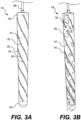
- FIG. 3A depicts a side plan view of device 116 while FIG. 3B depicts a side plan view of device 116 after an example plating process where material 153 has collected or otherwise build-up about portions 147 and openings 143.
- device 116 may include a cylindrical tube and/or a conduit that can be hollow and substantially elongated. Device 116 can extend vertically from a proximal end 216 to a distal end 214. Device 116 may also include a plurality of openings 143 (e.g., apertures, holes, slots, slits, ovals, perforations, etc.) that penetrate through the sidewall of device 116.
- openings 143 e.g., apertures, holes, slots, slits, ovals, perforations, etc.
- the openings 143 may have a diameter of less than about 2 inch, e.g., less than about 1 inch, less than about 0.75 inch, or less than about 0.5 inch. Openings 143 may be selectively extended and/or arranged on the sidewall in a continuous, spiral-shaped (or helical) surface that extends vertically between ends 216 and 214. In one embodiment, the size of each of openings 143 may be equal. However, the shape and size of each of openings 143, individually or in groups, may vary based on the shape and dimensions of one or more parts or work pieces (e.g., a shaft, rod, beam, cylinder, bar, etc.) being electroplated.
- parts or work pieces e.g., a shaft, rod, beam, cylinder, bar, etc.
- each opening may depend on the rotor diameter and the number of lobes on the rotor.
- openings 143 in the shield may be sized at 0.5 inch for 2 inch and 4 inch diameter rotors with 5 lobes. The diameter of the opening(s) may be increased for a rotor with a larger diameter.
- openings 143 in the shield may be sized between 1 and 2 inches for an 8 inch diameter rotor with 5 lobes.
- the size of the openings 143 may vary based on the distance between the shield and part 121 (e.g., rotor).
- Ends 216 and 214 may be "zones" that include a continuous, cylindrical surface between the respective end and beginning of openings 143 (e.g., a non-perforated zone).
- proximal and distal ends 216 and 214 of the part 121 may experience a higher electroplating rate compared to the rest of the part 121.
- a predetermined vertical length at each end of the part 121 may gain a thicker growth of electroplate coating layer compared to the rest of the part 121.
- device 116 may be arranged or placed within an electroplating chamber (e.g., the electroplating chamber 158) in the manner to cover at least about ends 214 and 216 of the part 121. Accordingly, a uniform electroplate coating layer may be formed on the part 121 by utilizing the electroplating shield device 116, in accordance with one or more aspects of the present disclosure.
- portions 147 of device 116 that form its sidewall around openings 143 can be made from a material including, for example, nickel-chromium alloys (e.g., ICONEL alloys, a registered trademark of Special Metals Corporation, mp 1390° C to 1425° C) or any other suitable stainless steels, high strength steels with high nickel content, and/or any other metal substrates with high nickel content having a melting point in excess of about 800°C materials that have a linear coefficient of thermal expansion (CTE) value substantially similar to ICONEL alloys.
- nickel-chromium alloys e.g., ICONEL alloys, a registered trademark of Special Metals Corporation, mp 1390° C to 1425° C
- any other suitable stainless steels e.g., high strength steels with high nickel content, and/or any other metal substrates with high nickel content having a melting point in excess of about 800°C materials that have a linear coefficient of thermal expansion (CTE) value substantially similar to ICONEL alloys.
- CTE linear coefficient
- the material used to form the sidewall around openings 143 may include iron alloys (e.g., iron-cobalt alloys, iron-nickel alloys, iron-tungsten alloys, and iron-chromium alloys etc.) and cobalt alloys (e.g., cobalt-chromium alloys).
- device 116 may or may not be conformal to part 121 and may or may not have though holes for targeted plating. Once the shape of part 121 has been determined, device 116 can receive a chemical resistant coating for longevity and to prevent buildup.
- Such a thin and lightweight construction for device 116 improves mobility and efficiency during electroplating processes, especially for electroplating large machinery parts (e.g., length greater than 20 feet) such as mud motor rotors. Further, the thin sidewall of device 116 may displace less electroplating solution, promote efficient electroplating solution movement, and may allow tighter electrode spacing, for example, in relatively smaller, enclosed electroplating chambers, especially when compared to prior chrome plating approaches which often require many start and stop cycles to ensure coating growth is even. By use of the inductive shielding of device 116, plating can be targeted to specific slow growth areas without added rectifier cost.
- device 116 acts like a shield to prevent excessive distribution for areas of high growth on part 121.
- one or more coatings may be applied to an outer surface of device 116 to improve corrosion resistance.
- coatings may include, for example, PVC, epoxy, and fluoropolymers (e.g., polytetrafluoroethylene (PTFE), ethylene tetrafluoroethylene (ETFE), fluorinated ethylene propylene (FEP), perfluoroalkoxy alkane (PFA), etc.).
- PTFE polytetrafluoroethylene
- ETFE ethylene tetrafluoroethylene
- FEP fluorinated ethylene propylene
- PFA perfluoroalkoxy alkane
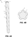
- FIG. 4A depicts an example part 121 processed using device 116 in an example electroplating chamber (e.g., chamber 158) of the electroplating system of FIG. 1A .
- FIG. 4B depicts an exemplary top plan cross-sectional view of part 121 taken at a middle portion of part 121 illustrating example minor regions F and major regions E.
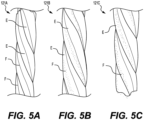
- FIG. 5A depicts a close-up of an upper portion 121A of part 121 as shown in FIG. 4A .
- FIG. 5B depicts a close-up of a middle portion 121B of part 121 as shown in FIG. 4A .
- FIG. 5C depicts a close-up of a lower portion 121C of part 121 as shown in FIG. 4A .
- FIGs. 5A to 5C illustrate example post-plating aspects of major regions E and minor regions F of part 121.
- FIG. 6 is a data plot diagram showing example measurements of part 121 processed and described in Figs. 3A to 5C .
- a mud motor rotor may include major regions (e.g., high/convex regions such as major regions E) that may be coated with electroplating deposits many times thicker than those of minor regions (e.g., low/concave regions such as minor regions F). Since the ratio of electroplating deposit thickness difference between the major regions and the minor regions can vary, the difference in the electroplating deposit thicknesses may leave the minor regions with a thinner-than-desired electroplate deposit thickness, which may result in reduced wear and corrosion resistance.
- each of openings 143 of device 116 may be varied based on the desired thickness of electroplating deposits on various regions of one or more parts or work pieces. Further, the density of openings 143 may also be varied based on the desired thickness of electroplating deposits on various regions of one or more parts or work pieces. With that, using the shield 116, 116' of FIGs. 3A to 3B , a pre-plating major diameter E of part 121 measured approximately 4.101 in, the post-plating major diameter E measured approximately 4.105 in, and the related post-plating major diameter E thickness measured approximately .004 in.
- the pre-plating minor diameter F of part 121 measured approximately 2.903 in
- the post-plating minor diameter F measured approximately 2.976 in
- the related post-plating minor diameter F thickness measured approximately .073 in.
- the major-to-minor ratio of plating with the example shield 116, 116' of FIGs. 3A to 3B was approximately 1:18 (major: minor or .073 in /.004 in) in contrast to plating without the herein disclosed inductive shield 116, which measured approximately 47:1 (major: minor).
- the advantageous improvement of the herein disclosed inductive shield therefore improves current throw into minor diameter F of part 121 thereby reducing additional plating processing which otherwise would be necessary and therefore saving production time and reduction of touch time.
- the heretofore describes use of both anode electrodes 162 and device 116 to produce a better distributed deposit on part 121, including through its major and minor regions, through use of inductive and/or bipolar current.
- the shape, size, and configuration of each of openings of the inductive shield device may be varied to achieve a major-to-minor plating ratio of approximately 1:1.
- the inductive shield device of the present disclosure has been configured to achieve a major-to-minor plating ratio of approximately 1:1, such that a ratio of thickness of the major region to the minor region is approximately 1:1, the electroplating operation may be performed in a single step.
- a method of fabricating an electroplating shield device of the present disclosure may include forming a plurality of openings on a strip and forming a conduit with the strip.
- Each of the openings may be varied to achieve a desired to major-to-minor plating ratio.
- the openings may be designed to transfer fluid to at least one of a first continuous section of an object (e.g., machinery part) comprising a minor of the object and a second continuous section of the object comprising a major of the object in a major-to-minor plating ratio.
- the major-to-minor plating ratio corresponding to a ratio of thickness achieved, may range from approximately 1:1 to approximately 1:18.
Landscapes
- Chemical & Material Sciences (AREA)
- Engineering & Computer Science (AREA)
- Chemical Kinetics & Catalysis (AREA)
- Electrochemistry (AREA)
- Materials Engineering (AREA)
- Metallurgy (AREA)
- Organic Chemistry (AREA)
- Electroplating Methods And Accessories (AREA)
- Treatment Of Fiber Materials (AREA)
Applications Claiming Priority (1)
| Application Number | Priority Date | Filing Date | Title |
|---|---|---|---|
| US17/934,121 US20240093400A1 (en) | 2022-09-21 | 2022-09-21 | Electroplating shield device |
Publications (2)
| Publication Number | Publication Date |
|---|---|
| EP4350054A2 true EP4350054A2 (de) | 2024-04-10 |
| EP4350054A3 EP4350054A3 (de) | 2024-06-19 |
Family
ID=87929318
Family Applications (1)
| Application Number | Title | Priority Date | Filing Date |
|---|---|---|---|
| EP23194890.2A Pending EP4350054A3 (de) | 2022-09-21 | 2023-09-01 | Elektroplattierungsabschirmungsvorrichtung |
Country Status (4)
| Country | Link |
|---|---|
| US (1) | US20240093400A1 (de) |
| EP (1) | EP4350054A3 (de) |
| CN (1) | CN117737813A (de) |
| CA (1) | CA3212338A1 (de) |
Family Cites Families (3)
| Publication number | Priority date | Publication date | Assignee | Title |
|---|---|---|---|---|
| US5098542A (en) * | 1990-09-11 | 1992-03-24 | Baker Hughes Incorporated | Controlled plating apparatus and method for irregularly-shaped objects |
| US20150132604A1 (en) * | 2013-11-14 | 2015-05-14 | National Oilwell DHT, L.P. | Multilayered Coating for Downhole Tools with Enhanced Wear Resistance and Acidic Corrosion Resistance |
| US12209323B2 (en) * | 2020-12-08 | 2025-01-28 | Honeywell International Inc. | Electroplating shield device and methods of fabricating the same |
-
2022
- 2022-09-21 US US17/934,121 patent/US20240093400A1/en not_active Abandoned
-
2023
- 2023-09-01 EP EP23194890.2A patent/EP4350054A3/de active Pending
- 2023-09-04 CN CN202311131723.0A patent/CN117737813A/zh active Pending
- 2023-09-13 CA CA3212338A patent/CA3212338A1/en active Pending
Also Published As
| Publication number | Publication date |
|---|---|
| EP4350054A3 (de) | 2024-06-19 |
| US20240093400A1 (en) | 2024-03-21 |
| CA3212338A1 (en) | 2024-03-21 |
| CN117737813A (zh) | 2024-03-22 |
Similar Documents
| Publication | Publication Date | Title |
|---|---|---|
| US5681443A (en) | Method for forming printed circuits | |
| JP6695799B2 (ja) | 軸受要素とその製造方法 | |
| US3065153A (en) | Electroplating method and apparatus | |
| TW201525172A (zh) | 具有低摩擦墊之物理氣相沉積標靶 | |
| US10392717B2 (en) | Protective coating for titanium last stage buckets | |
| JP2004509230A5 (de) | ||
| EP4350054A2 (de) | Elektroplattierungsabschirmungsvorrichtung | |
| CN111677759B (zh) | 将聚合物锚定到基底上的装置和方法 | |
| KR20190052895A (ko) | 전해 동박 제조 장치 | |
| US4080268A (en) | Method for high speed chromium plating of cylindrical articles | |
| RU2210620C1 (ru) | Способ ионно-плазменного нанесения многокомпонентных пленочных покрытий, мозаичная мишень для его осуществления и способ изготовления мишени | |
| US2761831A (en) | Electroplating fixture | |
| JPS6326395A (ja) | 金属篩の製造方法及び装置 | |
| US12209323B2 (en) | Electroplating shield device and methods of fabricating the same | |
| US2391039A (en) | Method of coating metal articles | |
| CN120261091A (zh) | 一种烧结钕铁硼磁体及其制备方法 | |
| CN111321452B (zh) | 深内孔零件挂镀结构 | |
| JPH03285097A (ja) | 電気めっき用陽極及び電気めっき方法 | |
| JPH09303289A (ja) | 分子ポンプの表面処理方法 | |
| JPS6344840B2 (de) | ||
| CN223280965U (zh) | 阳极材料的定位组件、定位机构及链条电镀装置 | |
| JP2017150000A (ja) | 部分めっき方法およびそれに用いるマスク部材 | |
| JP4604709B2 (ja) | 接合用部材およびそれを用いた器物 | |
| US20050145501A1 (en) | High energy plating process for static seals | |
| KR101176224B1 (ko) | 접합용 부재 및 그것을 이용한 기물 |
Legal Events
| Date | Code | Title | Description |
|---|---|---|---|
| PUAI | Public reference made under article 153(3) epc to a published international application that has entered the european phase |
Free format text: ORIGINAL CODE: 0009012 |
|
| STAA | Information on the status of an ep patent application or granted ep patent |
Free format text: STATUS: THE APPLICATION HAS BEEN PUBLISHED |
|
| AK | Designated contracting states |
Kind code of ref document: A2 Designated state(s): AL AT BE BG CH CY CZ DE DK EE ES FI FR GB GR HR HU IE IS IT LI LT LU LV MC ME MK MT NL NO PL PT RO RS SE SI SK SM TR |
|
| PUAL | Search report despatched |
Free format text: ORIGINAL CODE: 0009013 |
|
| AK | Designated contracting states |
Kind code of ref document: A3 Designated state(s): AL AT BE BG CH CY CZ DE DK EE ES FI FR GB GR HR HU IE IS IT LI LT LU LV MC ME MK MT NL NO PL PT RO RS SE SI SK SM TR |
|
| RIC1 | Information provided on ipc code assigned before grant |
Ipc: C25D 17/12 20060101ALN20240513BHEP Ipc: C25D 7/00 20060101ALI20240513BHEP Ipc: C25D 17/00 20060101ALI20240513BHEP Ipc: C25D 5/02 20060101AFI20240513BHEP |
|
| STAA | Information on the status of an ep patent application or granted ep patent |
Free format text: STATUS: REQUEST FOR EXAMINATION WAS MADE |
|
| 17P | Request for examination filed |
Effective date: 20240814 |
|
| RBV | Designated contracting states (corrected) |
Designated state(s): AL AT BE BG CH CY CZ DE DK EE ES FI FR GB GR HR HU IE IS IT LI LT LU LV MC ME MK MT NL NO PL PT RO RS SE SI SK SM TR |