EP4345856A1 - Multilayer electronic component - Google Patents
Multilayer electronic component Download PDFInfo
- Publication number
- EP4345856A1 EP4345856A1 EP23160431.5A EP23160431A EP4345856A1 EP 4345856 A1 EP4345856 A1 EP 4345856A1 EP 23160431 A EP23160431 A EP 23160431A EP 4345856 A1 EP4345856 A1 EP 4345856A1
- Authority
- EP
- European Patent Office
- Prior art keywords
- stabilized zirconia
- electronic component
- multilayer electronic
- dielectric
- dielectric layers
- Prior art date
- Legal status (The legal status is an assumption and is not a legal conclusion. Google has not performed a legal analysis and makes no representation as to the accuracy of the status listed.)
- Pending
Links
- 229910002076 stabilized zirconia Inorganic materials 0.000 claims abstract description 67
- 229910052726 zirconium Inorganic materials 0.000 claims description 51
- 239000000203 mixture Substances 0.000 claims description 46
- QCWXUUIWCKQGHC-UHFFFAOYSA-N Zirconium Chemical compound [Zr] QCWXUUIWCKQGHC-UHFFFAOYSA-N 0.000 claims description 45
- 229910001233 yttria-stabilized zirconia Inorganic materials 0.000 claims description 43
- 229910052727 yttrium Inorganic materials 0.000 claims description 43
- VWQVUPCCIRVNHF-UHFFFAOYSA-N yttrium atom Chemical compound [Y] VWQVUPCCIRVNHF-UHFFFAOYSA-N 0.000 claims description 37
- BRPQOXSCLDDYGP-UHFFFAOYSA-N calcium oxide Chemical compound [O-2].[Ca+2] BRPQOXSCLDDYGP-UHFFFAOYSA-N 0.000 claims description 6
- ODINCKMPIJJUCX-UHFFFAOYSA-N calcium oxide Inorganic materials [Ca]=O ODINCKMPIJJUCX-UHFFFAOYSA-N 0.000 claims description 6
- 239000000292 calcium oxide Substances 0.000 claims description 6
- 229910000420 cerium oxide Inorganic materials 0.000 claims description 6
- 239000000395 magnesium oxide Substances 0.000 claims description 6
- CPLXHLVBOLITMK-UHFFFAOYSA-N magnesium oxide Inorganic materials [Mg]=O CPLXHLVBOLITMK-UHFFFAOYSA-N 0.000 claims description 6
- AXZKOIWUVFPNLO-UHFFFAOYSA-N magnesium;oxygen(2-) Chemical compound [O-2].[Mg+2] AXZKOIWUVFPNLO-UHFFFAOYSA-N 0.000 claims description 6
- TWNQGVIAIRXVLR-UHFFFAOYSA-N oxo(oxoalumanyloxy)alumane Chemical compound O=[Al]O[Al]=O TWNQGVIAIRXVLR-UHFFFAOYSA-N 0.000 claims description 6
- BMMGVYCKOGBVEV-UHFFFAOYSA-N oxo(oxoceriooxy)cerium Chemical compound [Ce]=O.O=[Ce]=O BMMGVYCKOGBVEV-UHFFFAOYSA-N 0.000 claims description 6
- 239000010410 layer Substances 0.000 description 137
- BASFCYQUMIYNBI-UHFFFAOYSA-N platinum Chemical compound [Pt] BASFCYQUMIYNBI-UHFFFAOYSA-N 0.000 description 29
- 238000000034 method Methods 0.000 description 17
- PXHVJJICTQNCMI-UHFFFAOYSA-N Nickel Chemical compound [Ni] PXHVJJICTQNCMI-UHFFFAOYSA-N 0.000 description 16
- 238000007747 plating Methods 0.000 description 16
- 229910002113 barium titanate Inorganic materials 0.000 description 15
- 239000000463 material Substances 0.000 description 15
- 239000000843 powder Substances 0.000 description 14
- 229910052697 platinum Inorganic materials 0.000 description 13
- 238000005245 sintering Methods 0.000 description 13
- KDLHZDBZIXYQEI-UHFFFAOYSA-N Palladium Chemical compound [Pd] KDLHZDBZIXYQEI-UHFFFAOYSA-N 0.000 description 12
- 238000002354 inductively-coupled plasma atomic emission spectroscopy Methods 0.000 description 9
- 239000000919 ceramic Substances 0.000 description 8
- 238000004458 analytical method Methods 0.000 description 7
- 239000010936 titanium Substances 0.000 description 7
- 229910021642 ultra pure water Inorganic materials 0.000 description 7
- 239000012498 ultrapure water Substances 0.000 description 7
- MCMNRKCIXSYSNV-UHFFFAOYSA-N Zirconium dioxide Chemical compound O=[Zr]=O MCMNRKCIXSYSNV-UHFFFAOYSA-N 0.000 description 6
- 239000010949 copper Substances 0.000 description 6
- 239000010931 gold Substances 0.000 description 6
- 229910052751 metal Inorganic materials 0.000 description 6
- 239000002184 metal Substances 0.000 description 6
- JRPBQTZRNDNNOP-UHFFFAOYSA-N barium titanate Chemical compound [Ba+2].[Ba+2].[O-][Ti]([O-])([O-])[O-] JRPBQTZRNDNNOP-UHFFFAOYSA-N 0.000 description 5
- 239000011324 bead Substances 0.000 description 5
- 238000003801 milling Methods 0.000 description 5
- 238000004841 transmission electron microscopy energy-dispersive X-ray spectroscopy Methods 0.000 description 5
- ATJFFYVFTNAWJD-UHFFFAOYSA-N Tin Chemical compound [Sn] ATJFFYVFTNAWJD-UHFFFAOYSA-N 0.000 description 4
- 239000000956 alloy Substances 0.000 description 4
- 229910045601 alloy Inorganic materials 0.000 description 4
- 238000011088 calibration curve Methods 0.000 description 4
- 239000003985 ceramic capacitor Substances 0.000 description 4
- 229910010293 ceramic material Inorganic materials 0.000 description 4
- 238000004090 dissolution Methods 0.000 description 4
- 239000011521 glass Substances 0.000 description 4
- 239000012535 impurity Substances 0.000 description 4
- 229910052759 nickel Inorganic materials 0.000 description 4
- 229910052763 palladium Inorganic materials 0.000 description 4
- 239000000047 product Substances 0.000 description 4
- 238000004445 quantitative analysis Methods 0.000 description 4
- RYGMFSIKBFXOCR-UHFFFAOYSA-N Copper Chemical compound [Cu] RYGMFSIKBFXOCR-UHFFFAOYSA-N 0.000 description 3
- BQCADISMDOOEFD-UHFFFAOYSA-N Silver Chemical compound [Ag] BQCADISMDOOEFD-UHFFFAOYSA-N 0.000 description 3
- RTAQQCXQSZGOHL-UHFFFAOYSA-N Titanium Chemical compound [Ti] RTAQQCXQSZGOHL-UHFFFAOYSA-N 0.000 description 3
- 230000008901 benefit Effects 0.000 description 3
- 230000015572 biosynthetic process Effects 0.000 description 3
- 239000011575 calcium Substances 0.000 description 3
- 229910052802 copper Inorganic materials 0.000 description 3
- PCHJSUWPFVWCPO-UHFFFAOYSA-N gold Chemical compound [Au] PCHJSUWPFVWCPO-UHFFFAOYSA-N 0.000 description 3
- 229910052737 gold Inorganic materials 0.000 description 3
- 238000010438 heat treatment Methods 0.000 description 3
- 238000004519 manufacturing process Methods 0.000 description 3
- 239000011347 resin Substances 0.000 description 3
- 229920005989 resin Polymers 0.000 description 3
- VSZWPYCFIRKVQL-UHFFFAOYSA-N selanylidenegallium;selenium Chemical compound [Se].[Se]=[Ga].[Se]=[Ga] VSZWPYCFIRKVQL-UHFFFAOYSA-N 0.000 description 3
- 229910052709 silver Inorganic materials 0.000 description 3
- 239000004332 silver Substances 0.000 description 3
- 239000000126 substance Substances 0.000 description 3
- 229910052719 titanium Inorganic materials 0.000 description 3
- WFKWXMTUELFFGS-UHFFFAOYSA-N tungsten Chemical compound [W] WFKWXMTUELFFGS-UHFFFAOYSA-N 0.000 description 3
- 229910052721 tungsten Inorganic materials 0.000 description 3
- 239000010937 tungsten Substances 0.000 description 3
- RUDFQVOCFDJEEF-UHFFFAOYSA-N yttrium(III) oxide Inorganic materials [O-2].[O-2].[O-2].[Y+3].[Y+3] RUDFQVOCFDJEEF-UHFFFAOYSA-N 0.000 description 3
- 229910013178 LiBO2 Inorganic materials 0.000 description 2
- GRYLNZFGIOXLOG-UHFFFAOYSA-N Nitric acid Chemical compound O[N+]([O-])=O GRYLNZFGIOXLOG-UHFFFAOYSA-N 0.000 description 2
- 229910009650 Ti1-yZry Inorganic materials 0.000 description 2
- 239000000654 additive Substances 0.000 description 2
- 239000007864 aqueous solution Substances 0.000 description 2
- QVGXLLKOCUKJST-UHFFFAOYSA-N atomic oxygen Chemical compound [O] QVGXLLKOCUKJST-UHFFFAOYSA-N 0.000 description 2
- 230000015556 catabolic process Effects 0.000 description 2
- 239000002131 composite material Substances 0.000 description 2
- 238000009792 diffusion process Methods 0.000 description 2
- 238000007865 diluting Methods 0.000 description 2
- 230000000694 effects Effects 0.000 description 2
- 239000000706 filtrate Substances 0.000 description 2
- HZRMTWQRDMYLNW-UHFFFAOYSA-N lithium metaborate Chemical compound [Li+].[O-]B=O HZRMTWQRDMYLNW-UHFFFAOYSA-N 0.000 description 2
- 238000005259 measurement Methods 0.000 description 2
- 150000002739 metals Chemical class 0.000 description 2
- 230000004048 modification Effects 0.000 description 2
- 238000012986 modification Methods 0.000 description 2
- 229910017604 nitric acid Inorganic materials 0.000 description 2
- 229910052760 oxygen Inorganic materials 0.000 description 2
- 239000001301 oxygen Substances 0.000 description 2
- 239000002994 raw material Substances 0.000 description 2
- OYPRJOBELJOOCE-UHFFFAOYSA-N Calcium Chemical compound [Ca] OYPRJOBELJOOCE-UHFFFAOYSA-N 0.000 description 1
- 229910010252 TiO3 Inorganic materials 0.000 description 1
- 239000002253 acid Substances 0.000 description 1
- 230000009286 beneficial effect Effects 0.000 description 1
- 239000011230 binding agent Substances 0.000 description 1
- 229910052791 calcium Inorganic materials 0.000 description 1
- 230000000052 comparative effect Effects 0.000 description 1
- 230000008602 contraction Effects 0.000 description 1
- 230000008094 contradictory effect Effects 0.000 description 1
- 238000000354 decomposition reaction Methods 0.000 description 1
- 230000007423 decrease Effects 0.000 description 1
- 238000001514 detection method Methods 0.000 description 1
- 239000002270 dispersing agent Substances 0.000 description 1
- 230000005611 electricity Effects 0.000 description 1
- 238000011156 evaluation Methods 0.000 description 1
- 239000012467 final product Substances 0.000 description 1
- -1 for example Inorganic materials 0.000 description 1
- 238000007646 gravure printing Methods 0.000 description 1
- 238000000227 grinding Methods 0.000 description 1
- 238000003384 imaging method Methods 0.000 description 1
- 150000002500 ions Chemical class 0.000 description 1
- 239000004973 liquid crystal related substance Substances 0.000 description 1
- 239000003960 organic solvent Substances 0.000 description 1
- RVTZCBVAJQQJTK-UHFFFAOYSA-N oxygen(2-);zirconium(4+) Chemical compound [O-2].[O-2].[Zr+4] RVTZCBVAJQQJTK-UHFFFAOYSA-N 0.000 description 1
- 230000002093 peripheral effect Effects 0.000 description 1
- 238000007639 printing Methods 0.000 description 1
- 231100000628 reference dose Toxicity 0.000 description 1
- 238000007650 screen-printing Methods 0.000 description 1
- 239000002356 single layer Substances 0.000 description 1
- 239000003381 stabilizer Substances 0.000 description 1
- VEALVRVVWBQVSL-UHFFFAOYSA-N strontium titanate Chemical compound [Sr+2].[O-][Ti]([O-])=O VEALVRVVWBQVSL-UHFFFAOYSA-N 0.000 description 1
- 238000006467 substitution reaction Methods 0.000 description 1
- 229910001928 zirconium oxide Inorganic materials 0.000 description 1
Images


Classifications
-
- H—ELECTRICITY
- H01—ELECTRIC ELEMENTS
- H01G—CAPACITORS; CAPACITORS, RECTIFIERS, DETECTORS, SWITCHING DEVICES, LIGHT-SENSITIVE OR TEMPERATURE-SENSITIVE DEVICES OF THE ELECTROLYTIC TYPE
- H01G4/00—Fixed capacitors; Processes of their manufacture
- H01G4/002—Details
- H01G4/018—Dielectrics
- H01G4/06—Solid dielectrics
- H01G4/08—Inorganic dielectrics
- H01G4/12—Ceramic dielectrics
- H01G4/1209—Ceramic dielectrics characterised by the ceramic dielectric material
-
- H—ELECTRICITY
- H01—ELECTRIC ELEMENTS
- H01G—CAPACITORS; CAPACITORS, RECTIFIERS, DETECTORS, SWITCHING DEVICES, LIGHT-SENSITIVE OR TEMPERATURE-SENSITIVE DEVICES OF THE ELECTROLYTIC TYPE
- H01G4/00—Fixed capacitors; Processes of their manufacture
- H01G4/002—Details
- H01G4/018—Dielectrics
- H01G4/06—Solid dielectrics
- H01G4/08—Inorganic dielectrics
- H01G4/12—Ceramic dielectrics
- H01G4/1209—Ceramic dielectrics characterised by the ceramic dielectric material
- H01G4/1236—Ceramic dielectrics characterised by the ceramic dielectric material based on zirconium oxides or zirconates
-
- H—ELECTRICITY
- H01—ELECTRIC ELEMENTS
- H01G—CAPACITORS; CAPACITORS, RECTIFIERS, DETECTORS, SWITCHING DEVICES, LIGHT-SENSITIVE OR TEMPERATURE-SENSITIVE DEVICES OF THE ELECTROLYTIC TYPE
- H01G4/00—Fixed capacitors; Processes of their manufacture
- H01G4/30—Stacked capacitors
-
- B—PERFORMING OPERATIONS; TRANSPORTING
- B32—LAYERED PRODUCTS
- B32B—LAYERED PRODUCTS, i.e. PRODUCTS BUILT-UP OF STRATA OF FLAT OR NON-FLAT, e.g. CELLULAR OR HONEYCOMB, FORM
- B32B18/00—Layered products essentially comprising ceramics, e.g. refractory products
-
- C—CHEMISTRY; METALLURGY
- C04—CEMENTS; CONCRETE; ARTIFICIAL STONE; CERAMICS; REFRACTORIES
- C04B—LIME, MAGNESIA; SLAG; CEMENTS; COMPOSITIONS THEREOF, e.g. MORTARS, CONCRETE OR LIKE BUILDING MATERIALS; ARTIFICIAL STONE; CERAMICS; REFRACTORIES; TREATMENT OF NATURAL STONE
- C04B35/00—Shaped ceramic products characterised by their composition; Ceramics compositions; Processing powders of inorganic compounds preparatory to the manufacturing of ceramic products
- C04B35/01—Shaped ceramic products characterised by their composition; Ceramics compositions; Processing powders of inorganic compounds preparatory to the manufacturing of ceramic products based on oxide ceramics
- C04B35/46—Shaped ceramic products characterised by their composition; Ceramics compositions; Processing powders of inorganic compounds preparatory to the manufacturing of ceramic products based on oxide ceramics based on titanium oxides or titanates
- C04B35/462—Shaped ceramic products characterised by their composition; Ceramics compositions; Processing powders of inorganic compounds preparatory to the manufacturing of ceramic products based on oxide ceramics based on titanium oxides or titanates based on titanates
- C04B35/465—Shaped ceramic products characterised by their composition; Ceramics compositions; Processing powders of inorganic compounds preparatory to the manufacturing of ceramic products based on oxide ceramics based on titanium oxides or titanates based on titanates based on alkaline earth metal titanates
- C04B35/468—Shaped ceramic products characterised by their composition; Ceramics compositions; Processing powders of inorganic compounds preparatory to the manufacturing of ceramic products based on oxide ceramics based on titanium oxides or titanates based on titanates based on alkaline earth metal titanates based on barium titanates
- C04B35/4682—Shaped ceramic products characterised by their composition; Ceramics compositions; Processing powders of inorganic compounds preparatory to the manufacturing of ceramic products based on oxide ceramics based on titanium oxides or titanates based on titanates based on alkaline earth metal titanates based on barium titanates based on BaTiO3 perovskite phase
-
- C—CHEMISTRY; METALLURGY
- C04—CEMENTS; CONCRETE; ARTIFICIAL STONE; CERAMICS; REFRACTORIES
- C04B—LIME, MAGNESIA; SLAG; CEMENTS; COMPOSITIONS THEREOF, e.g. MORTARS, CONCRETE OR LIKE BUILDING MATERIALS; ARTIFICIAL STONE; CERAMICS; REFRACTORIES; TREATMENT OF NATURAL STONE
- C04B35/00—Shaped ceramic products characterised by their composition; Ceramics compositions; Processing powders of inorganic compounds preparatory to the manufacturing of ceramic products
- C04B35/622—Forming processes; Processing powders of inorganic compounds preparatory to the manufacturing of ceramic products
- C04B35/626—Preparing or treating the powders individually or as batches ; preparing or treating macroscopic reinforcing agents for ceramic products, e.g. fibres; mechanical aspects section B
- C04B35/62605—Treating the starting powders individually or as mixtures
- C04B35/6261—Milling
-
- H—ELECTRICITY
- H01—ELECTRIC ELEMENTS
- H01G—CAPACITORS; CAPACITORS, RECTIFIERS, DETECTORS, SWITCHING DEVICES, LIGHT-SENSITIVE OR TEMPERATURE-SENSITIVE DEVICES OF THE ELECTROLYTIC TYPE
- H01G4/00—Fixed capacitors; Processes of their manufacture
- H01G4/002—Details
- H01G4/005—Electrodes
- H01G4/012—Form of non-self-supporting electrodes
-
- H—ELECTRICITY
- H01—ELECTRIC ELEMENTS
- H01G—CAPACITORS; CAPACITORS, RECTIFIERS, DETECTORS, SWITCHING DEVICES, LIGHT-SENSITIVE OR TEMPERATURE-SENSITIVE DEVICES OF THE ELECTROLYTIC TYPE
- H01G4/00—Fixed capacitors; Processes of their manufacture
- H01G4/002—Details
- H01G4/018—Dielectrics
- H01G4/06—Solid dielectrics
- H01G4/08—Inorganic dielectrics
- H01G4/12—Ceramic dielectrics
- H01G4/1209—Ceramic dielectrics characterised by the ceramic dielectric material
- H01G4/1218—Ceramic dielectrics characterised by the ceramic dielectric material based on titanium oxides or titanates
-
- H—ELECTRICITY
- H01—ELECTRIC ELEMENTS
- H01G—CAPACITORS; CAPACITORS, RECTIFIERS, DETECTORS, SWITCHING DEVICES, LIGHT-SENSITIVE OR TEMPERATURE-SENSITIVE DEVICES OF THE ELECTROLYTIC TYPE
- H01G4/00—Fixed capacitors; Processes of their manufacture
- H01G4/002—Details
- H01G4/018—Dielectrics
- H01G4/06—Solid dielectrics
- H01G4/08—Inorganic dielectrics
- H01G4/12—Ceramic dielectrics
- H01G4/1209—Ceramic dielectrics characterised by the ceramic dielectric material
- H01G4/1218—Ceramic dielectrics characterised by the ceramic dielectric material based on titanium oxides or titanates
- H01G4/1227—Ceramic dielectrics characterised by the ceramic dielectric material based on titanium oxides or titanates based on alkaline earth titanates
-
- C—CHEMISTRY; METALLURGY
- C04—CEMENTS; CONCRETE; ARTIFICIAL STONE; CERAMICS; REFRACTORIES
- C04B—LIME, MAGNESIA; SLAG; CEMENTS; COMPOSITIONS THEREOF, e.g. MORTARS, CONCRETE OR LIKE BUILDING MATERIALS; ARTIFICIAL STONE; CERAMICS; REFRACTORIES; TREATMENT OF NATURAL STONE
- C04B2235/00—Aspects relating to ceramic starting mixtures or sintered ceramic products
- C04B2235/02—Composition of constituents of the starting material or of secondary phases of the final product
- C04B2235/30—Constituents and secondary phases not being of a fibrous nature
- C04B2235/32—Metal oxides, mixed metal oxides, or oxide-forming salts thereof, e.g. carbonates, nitrates, (oxy)hydroxides, chlorides
- C04B2235/3205—Alkaline earth oxides or oxide forming salts thereof, e.g. beryllium oxide
- C04B2235/3206—Magnesium oxides or oxide-forming salts thereof
-
- C—CHEMISTRY; METALLURGY
- C04—CEMENTS; CONCRETE; ARTIFICIAL STONE; CERAMICS; REFRACTORIES
- C04B—LIME, MAGNESIA; SLAG; CEMENTS; COMPOSITIONS THEREOF, e.g. MORTARS, CONCRETE OR LIKE BUILDING MATERIALS; ARTIFICIAL STONE; CERAMICS; REFRACTORIES; TREATMENT OF NATURAL STONE
- C04B2235/00—Aspects relating to ceramic starting mixtures or sintered ceramic products
- C04B2235/02—Composition of constituents of the starting material or of secondary phases of the final product
- C04B2235/30—Constituents and secondary phases not being of a fibrous nature
- C04B2235/32—Metal oxides, mixed metal oxides, or oxide-forming salts thereof, e.g. carbonates, nitrates, (oxy)hydroxides, chlorides
- C04B2235/3205—Alkaline earth oxides or oxide forming salts thereof, e.g. beryllium oxide
- C04B2235/3208—Calcium oxide or oxide-forming salts thereof, e.g. lime
-
- C—CHEMISTRY; METALLURGY
- C04—CEMENTS; CONCRETE; ARTIFICIAL STONE; CERAMICS; REFRACTORIES
- C04B—LIME, MAGNESIA; SLAG; CEMENTS; COMPOSITIONS THEREOF, e.g. MORTARS, CONCRETE OR LIKE BUILDING MATERIALS; ARTIFICIAL STONE; CERAMICS; REFRACTORIES; TREATMENT OF NATURAL STONE
- C04B2235/00—Aspects relating to ceramic starting mixtures or sintered ceramic products
- C04B2235/02—Composition of constituents of the starting material or of secondary phases of the final product
- C04B2235/30—Constituents and secondary phases not being of a fibrous nature
- C04B2235/32—Metal oxides, mixed metal oxides, or oxide-forming salts thereof, e.g. carbonates, nitrates, (oxy)hydroxides, chlorides
- C04B2235/3217—Aluminum oxide or oxide forming salts thereof, e.g. bauxite, alpha-alumina
-
- C—CHEMISTRY; METALLURGY
- C04—CEMENTS; CONCRETE; ARTIFICIAL STONE; CERAMICS; REFRACTORIES
- C04B—LIME, MAGNESIA; SLAG; CEMENTS; COMPOSITIONS THEREOF, e.g. MORTARS, CONCRETE OR LIKE BUILDING MATERIALS; ARTIFICIAL STONE; CERAMICS; REFRACTORIES; TREATMENT OF NATURAL STONE
- C04B2235/00—Aspects relating to ceramic starting mixtures or sintered ceramic products
- C04B2235/02—Composition of constituents of the starting material or of secondary phases of the final product
- C04B2235/30—Constituents and secondary phases not being of a fibrous nature
- C04B2235/32—Metal oxides, mixed metal oxides, or oxide-forming salts thereof, e.g. carbonates, nitrates, (oxy)hydroxides, chlorides
- C04B2235/3224—Rare earth oxide or oxide forming salts thereof, e.g. scandium oxide
- C04B2235/3225—Yttrium oxide or oxide-forming salts thereof
-
- C—CHEMISTRY; METALLURGY
- C04—CEMENTS; CONCRETE; ARTIFICIAL STONE; CERAMICS; REFRACTORIES
- C04B—LIME, MAGNESIA; SLAG; CEMENTS; COMPOSITIONS THEREOF, e.g. MORTARS, CONCRETE OR LIKE BUILDING MATERIALS; ARTIFICIAL STONE; CERAMICS; REFRACTORIES; TREATMENT OF NATURAL STONE
- C04B2235/00—Aspects relating to ceramic starting mixtures or sintered ceramic products
- C04B2235/02—Composition of constituents of the starting material or of secondary phases of the final product
- C04B2235/30—Constituents and secondary phases not being of a fibrous nature
- C04B2235/32—Metal oxides, mixed metal oxides, or oxide-forming salts thereof, e.g. carbonates, nitrates, (oxy)hydroxides, chlorides
- C04B2235/3224—Rare earth oxide or oxide forming salts thereof, e.g. scandium oxide
- C04B2235/3229—Cerium oxides or oxide-forming salts thereof
-
- C—CHEMISTRY; METALLURGY
- C04—CEMENTS; CONCRETE; ARTIFICIAL STONE; CERAMICS; REFRACTORIES
- C04B—LIME, MAGNESIA; SLAG; CEMENTS; COMPOSITIONS THEREOF, e.g. MORTARS, CONCRETE OR LIKE BUILDING MATERIALS; ARTIFICIAL STONE; CERAMICS; REFRACTORIES; TREATMENT OF NATURAL STONE
- C04B2235/00—Aspects relating to ceramic starting mixtures or sintered ceramic products
- C04B2235/02—Composition of constituents of the starting material or of secondary phases of the final product
- C04B2235/30—Constituents and secondary phases not being of a fibrous nature
- C04B2235/32—Metal oxides, mixed metal oxides, or oxide-forming salts thereof, e.g. carbonates, nitrates, (oxy)hydroxides, chlorides
- C04B2235/3231—Refractory metal oxides, their mixed metal oxides, or oxide-forming salts thereof
- C04B2235/3244—Zirconium oxides, zirconates, hafnium oxides, hafnates, or oxide-forming salts thereof
- C04B2235/3246—Stabilised zirconias, e.g. YSZ or cerium stabilised zirconia
-
- C—CHEMISTRY; METALLURGY
- C04—CEMENTS; CONCRETE; ARTIFICIAL STONE; CERAMICS; REFRACTORIES
- C04B—LIME, MAGNESIA; SLAG; CEMENTS; COMPOSITIONS THEREOF, e.g. MORTARS, CONCRETE OR LIKE BUILDING MATERIALS; ARTIFICIAL STONE; CERAMICS; REFRACTORIES; TREATMENT OF NATURAL STONE
- C04B2235/00—Aspects relating to ceramic starting mixtures or sintered ceramic products
- C04B2235/70—Aspects relating to sintered or melt-casted ceramic products
- C04B2235/72—Products characterised by the absence or the low content of specific components, e.g. alkali metal free alumina ceramics
-
- C—CHEMISTRY; METALLURGY
- C04—CEMENTS; CONCRETE; ARTIFICIAL STONE; CERAMICS; REFRACTORIES
- C04B—LIME, MAGNESIA; SLAG; CEMENTS; COMPOSITIONS THEREOF, e.g. MORTARS, CONCRETE OR LIKE BUILDING MATERIALS; ARTIFICIAL STONE; CERAMICS; REFRACTORIES; TREATMENT OF NATURAL STONE
- C04B2237/00—Aspects relating to ceramic laminates or to joining of ceramic articles with other articles by heating
- C04B2237/30—Composition of layers of ceramic laminates or of ceramic or metallic articles to be joined by heating, e.g. Si substrates
- C04B2237/32—Ceramic
- C04B2237/34—Oxidic
- C04B2237/345—Refractory metal oxides
- C04B2237/346—Titania or titanates
-
- C—CHEMISTRY; METALLURGY
- C04—CEMENTS; CONCRETE; ARTIFICIAL STONE; CERAMICS; REFRACTORIES
- C04B—LIME, MAGNESIA; SLAG; CEMENTS; COMPOSITIONS THEREOF, e.g. MORTARS, CONCRETE OR LIKE BUILDING MATERIALS; ARTIFICIAL STONE; CERAMICS; REFRACTORIES; TREATMENT OF NATURAL STONE
- C04B2237/00—Aspects relating to ceramic laminates or to joining of ceramic articles with other articles by heating
- C04B2237/50—Processing aspects relating to ceramic laminates or to the joining of ceramic articles with other articles by heating
- C04B2237/58—Forming a gradient in composition or in properties across the laminate or the joined articles
Definitions
- the present disclosure relates to a multilayer electronic component.
- a multilayer ceramic capacitor (MLCC) that is one of the multilayer electronic components is a chip-type condenser mounted on a printed circuit board of various electronic products such as imaging devices like a liquid crystal display device (LCD) and a plasma display device panel (PDP), computers, smartphones, and serves to charge or discharge electricity.
- imaging devices like a liquid crystal display device (LCD) and a plasma display device panel (PDP)
- LCD liquid crystal display device
- PDP plasma display device panel
- multilayer ceramic capacitors may be used as components in a variety of electronic devices thanks to their small sizes, high capacity, and ease of mounting.
- electronic devices such as computers and mobile devices have become miniaturized and capable of high-output, the demand for miniaturization and higher capacity for multilayer ceramic capacitors is increasing.
- a milling process may be used to atomize the dielectric powders, in which zirconium beads may be used as a media. Due to the characteristics of the milling process, zirconium (Zr), a component of zirconium beads, may be introduced into the dielectric powder as an impurity, and the zirconium introduced as an impurity has been identified as a factor that may affect various characteristics such as electrical properties, dielectric capacity, a dissipation factor (DF), and breakdown voltage (BDV) of the dielectric powder.
- Zr zirconium
- DF dissipation factor
- BDV breakdown voltage
- An aspect of the present disclosure is to provide multilayer electronic components with improved electrical properties, dielectric capacity, DF and BDV, etc. by adding stabilized zirconia to the dielectric composition.
- a multilayer electronic component comprises an active portion including first dielectric layers, where at least one of the first dielectric layers includes stabilized zirconia, and first and second internal electrodes alternately disposed between the first dielectric layers to form capacitance, a body including first and second surfaces opposing each other in a first direction, third and fourth surfaces connected to the first and second surfaces and opposing each other in a second direction, and fifth and sixth surfaces connected to the first to fourth surfaces and opposing each other in a third direction; and first and second external electrodes disposed on the body and connected to the first and second internal electrodes, respectively.
- the multilayer electronic component comprises a body including an active portion including a first dielectric layers, first and second internal electrodes alternately disposed between the first dielectric layers to form capacitance, and first and second surfaces opposing each other in a first direction, third and fourth surfaces connected to the first and second surfaces and opposing each other in a second direction, and fifth and sixth surfaces connected to the first to fourth surfaces and opposing each other in a third direction; and including first and second external electrodes disposed on the body and connected to the first and second internal electrodes, respectively, wherein at least one of the first dielectric layers includes a first dielectric composition, the first dielectric composition comprises stabilized zirconia, the stabilized zirconia may contain one or more of yttria stabilized zirconia, magnesium oxide stabilized zirconia, cerium oxide stabilized zirconia, aluminum oxide stabilized zirconia, and calcium oxide stabilized zirconia.
- a first direction may be defined as a stacking direction or a thickness T direction, a second direction as a length L direction, and a third direction as a width W direction.
- FIG. 1 is a perspective view of a multilayer electronic component according to an embodiment of the present disclosure.
- FIG. 2 is a schematic exploded view of a body of the multilayer electronic component according to an embodiment of the present disclosure.
- FIG. 3 is a view schematically illustrating a cross section taken along line I-I' of FIG. 1 .
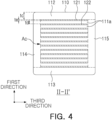
- FIG. 4 is a view schematically illustrating a cross section taken along line II-II' of FIG. 1 .
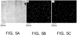
- FIG. 5 is an image captured by TEM-EDS of a first dielectric layer of the multilayer electronic component according to an embodiment of the present disclosure.
- a multilayer electronic component according to an embodiment of the present disclosure will be described in detail.
- a multilayer electronic component a multilayer ceramic capacitor will be described, but the present disclosure may be applied to various electronic products using a dielectric composition, such as, an inductor, a piezoelectric device, a varistor, or a thermistor.
- the multilayer electronic component 100 comprises a body including an active portion Ac including a plurality of first dielectric layers 111a and first and second internal electrodes 121 and 122 alternately disposed between the first dielectric layers 111a to form capacitance, a body comprising first and second surfaces 1 and 2 opposing each other in a first direction, and third and fourth surfaces 3 and 4 connected to the first and second surfaces 1 and 2 and opposing each other in a second direction, and fifth and sixth surfaces 5 and 6 connected to the first to fourth surfaces 1, 2, 3 and 4 and opposing each other in a third direction; and first and second external electrodes 131 and 132 disposed on the body 110 and connected to the first and second internal electrodes 121 and 122, respectively, wherein the first dielectric layer 111a may comprise stabilized zirconia.
- the "dielectric layer” may refer to a first dielectric layer 111a included in the active portion Ac, a second dielectric layer 111b included in cover portions 112 and 113, and a third dielectric layer 111c included in the margin portions 114 and 115.
- a detailed description of the first to third dielectric layers 111a , 111b, and 111c will be described below.
- peripheral portion may refer to a cover portion as disclosed herein, a margin portion as disclosed herein, or both.
- a body 110 includes the first dielectric layer 111a alternately stacked with the internal electrodes 121 and 122.
- a body 110 is disposed inside the body 110 and includes the first internal electrode 121 and the second internal electrode 122 that are alternately disposed opposing each other with the first dielectric layer 111a in between.
- the body 110 may be made of a cube shape or a similar shape. Due to the contraction of the ceramic powder contained in the body 110 during the sintering process, the body 110 may not have a hexahedral shape with complete straight lines, but a substantial hexahedral shape.
- the body 110 may comprise the first and second surfaces 1 and 2 that face each other in the first direction, and the third and fourth surfaces 3 and 4 that are connected to the first and second surfaces 1 and 2 opposing each other in the second direction, and the fifth and sixth surfaces 5 and 6 that are connected to the first to the fourth surfaces 1, 2, 3 and 4 opposing each other in the third direction.
- the plurality of first dielectric layers 111a forming the body 110 are in a calcined state, and the border between the adjacent first dielectric layers 111a may be integrated so that it is difficult to check unless using a scanning electron microscope (SEM).
- SEM scanning electron microscope
- the raw material forming the first dielectric layer 111a is not limited as long as sufficient capacitance can be obtained.
- perovskite (ABO 3 ) based materials may be used, for example, barium titanate materials, lead composite perovskite materials, or strontium titanium oxide-based materials.
- Barium titanate materials may include BaTiO 3 based ceramic powders.
- BaTiO 3 and (Ba 1-x Ca x ) TiO 3 (0 ⁇ x ⁇ 1), Ba(Ti 1-y Ca y )O 3 (0 ⁇ y ⁇ 1), (Ba 1-x Ca x )(Ti 1-y Zr y )0 3 (0 ⁇ x ⁇ 1, 0 ⁇ y ⁇ 1) or Ba(Ti 1-y Zr y )O 3 (0 ⁇ y ⁇ 1), which are BaTiO 3 with partially employed Ca(calcium) and Zr(zirconium), etc., may be used as examples of ceramic powders.
- the raw material for forming the first dielectric layer 111a may be powders such as barium titanate (BaTiO 3 ) to which various ceramic additives, organic solvents, binders, dispersants, and etc., are added according to the object of the present disclosure.
- barium titanate BaTiO 3
- various ceramic additives, organic solvents, binders, dispersants, and etc. are added according to the object of the present disclosure.
- zirconium beads may be used as a media. Due to the nature of the milling process, zirconium (Zr), a component of zirconium beads, may be introduced into the dielectric powder as an impurity, and the zirconium introduced as an impurity has been identified as a factor that may affect various characteristics such as electrical properties, dielectric capacitance, DF (dissipation factor), and BDV (breakdown voltage) of the dielectric powder.
- Zr zirconium
- the zirconium currently has difficulty controlling its content and relies only on inflow control.
- stabilized zirconia may be added to the dielectric composition to improve the electrical properties, capacitive properties, DF and BDV properties of the multilayer electronic component.
- the first dielectric layer 111a included in the active portion Ac forming the capacitance may comprise stabilized zirconia.
- the stabilized zirconia may include one or more of the following: yttria-stabilized zirconia, magnesium oxide stabilized zirconia, cerium oxide stabilized zirconia, aluminum oxide stabilized zirconia and calcium oxide stabilized zirconia.
- Stabilized zirconia may be defined as a material in which a stabilizer is added to zirconium in order to prevent problems such as grain collapse that may follow when a volume change occurs due to the temperature change of zirconium.
- yttria stabilized zirconia corresponds to a material made to be stable at room temperature by adding yttrium acid (yttria) to zirconium oxide (zirconia).
- zirconia zirconium oxide
- yttria stabilized zirconia By adding yttria to zirconia, some of the Zr4+ ions are replaced by Y3+. This replaces four O2- ions with three O2- ions, resulting in an oxygen vacancy.
- yttria stabilized zirconia has O2-ion conductivity, and the higher the temperature gets, the better the conductivity becomes, and the toughness and strength may also be improved.
- the type of stabilized zirconia is not limited to the above-described type, and according to the type of beads used as a media in the milling process, or when the electrical properties are to be improved in various environments, the necessary kind of stabilized zirconia may be added.
- first dielectric layer 111a may be formed using a first dielectric composition, and the first dielectric composition may comprise stabilized zirconia.
- Stabilized zirconia added to the first dielectric composition may play the role of a sintering accelerator of the dielectric powder, and accordingly, the dielectric grain grows during the sintering process, and the dielectric permittivity is increased, thereby increasing the capacitance. That is, when stabilized zirconia is added to the first dielectric composition to form the first dielectric layer 111a , the electrical properties of the active portion Ac may be improved.
- YSZ yttria stabilized zirconia
- BT BaTiO 3
- YSZ may remain as YSZ without decomposition even after sintering, or some may be decomposed into Y and Zr, or all YSZ may be decomposed into Y and Zr. At this time, even if YSZ is formed as in the form of YSZ, Y and Zr, electrical properties can be improved. Accordingly, appropriate control is preferably performed according to the manufacturing process.
- the electrical properties may be improved, and it may be desirable to add at least 200 ppm.
- At least one of the plurality of first dielectric layers 111a included in the active portion Ac may comprise zirconium.
- At least one of the plurality of first dielectric layers 111a included in the active portion Ac may comprise yttrium.
- Zirconium and yttrium included in the first dielectric layer 111a may be the result of the detection of zirconium or yttrium elements in the first dielectric layer 111a as stabilized zirconia, with the addition of yttria stabilized zirconia to the first dielectric composition.
- a component analysis of yttria stabilized zirconia, zirconium and yttrium may be performed using transmission electron microscopy-energy dispersive X-ray spectroscopy (TEM-EDS).
- TEM-EDS transmission electron microscopy-energy dispersive X-ray spectroscopy
- any first dielectric layer 111a may be analyzed by TEM-EDS to proceed with component analysis.
- components of yttria stabilized zirconia, zirconium and yttrium located in an area set based on the center point of a cross-section of the first and second directions may be analyzed.
- yttria stabilized zirconia, zirconium and yttrium may be quantitatively analyzed using inductively coupled plasma optical emission spectroscopy (ICP-OES) equipment.
- ICP-OES inductively coupled plasma optical emission spectroscopy
- the pretreatment conditions are important, and the pretreatment conditions are as follows:
- sample chip and 1 ⁇ 2g of LiBO 2 are diluted 10-20 times, placed in a platinum crucible, and melted at a temperature of 1050°C for 3 hours.
- the molten platinum crucible is inserted into a 250 ml beaker (low 250 ml) and a 10% concentration of nitric acid aqueous solution is poured until the platinum crucible is submerged (about 200 ml).
- the beaker is covered with a watch glass and the ultrasonic dissolution is proceeded in a 60 ⁇ 70°C thermostatic bath for 60 minutes. At this time, the ultrasonic dissolution is carried out until there is no residue inside the platinum crucible.
- the Perkin Elmer Avio 200 device may then be used to quantitatively analyze zirconium and yttrium content.
- the calibration curve may be set by diluting 10, 100 and 1000 times using a standard sample, and it may be considered effective when 99.99% or more is satisfied.
- ppm of quantified samples may be analyzed.
- the content measured by this way may mean an average content.
- the thickness td of the first dielectric layer 111a does not need to be particularly limited.
- the thickness of the first dielectric layer 111a may be 0.6 um or less, more preferably 0.4 ⁇ m or less.
- the thickness td of the first dielectric layer 111a may mean the thickness of the second dielectric layer 111b and the third dielectric layer (not shown) described below.
- the thickness td of the first dielectric layer 111a may mean the thickness td of the first dielectric layer 111a disposed between the first and second internal electrodes 121 and 122.
- the thickness td of the first dielectric layer 111a may mean the size of the first dielectric layer 111a along the first direction.
- the thickness td of the first dielectric layer 111a may mean the average thickness td of the first dielectric layer 111a and the average size the first dielectric layer 111a along the first direction.
- the average size of the first dielectric layer 111a along the first direction may be measured by scanning the images of the cross-sections of the first and second directions of the body 110 with a scanning electron microscope (SEM) at 10,000 magnifications. More specifically, it may be an average value measuring the size of the first dielectric layer 111a along the first direction at 30 equidistant interval points in the second direction in order to measure one first dielectric layer 111a from a scanned image. The 30 equidistant interval points may be designated in the active portion Ac.
- the average value measurement is extended to 10 first dielectric layers 111a to measure the average value, the average size of the first dielectric layer 111a along the first direction may be further generalized. Other methods and/or tools appreciated by one of ordinary skill in the art, even if not described in the present disclosure, may also be used.
- the internal electrodes 121 and 122 may be alternately stacked with the first dielectric layer 111a.
- the internal electrodes 121 and 122 may include a first internal electrode 121 and a second internal electrode 122, and the first and second internal electrodes 121 and 122 are alternately arranged to face each other with the first dielectric layer 111a in between that constitutes the body 110, and may be exposed to the third and fourth surfaces 3 and 4, respectively, of the body 110.
- first internal electrode 121 is spaced apart from the fourth surface 4 and may be exposed through the third surface 3
- second internal electrode 122 is spaced apart from the third surface 3 and may be exposed through the fourth surface 4.
- the first external electrode 131 is disposed on the third surface 3 of the body 110 and connected to the first internal electrode 121
- the second external electrode 132 is disposed on the fourth surface 4 of the body 110 and connected to the second internal electrode 122.
- the first internal electrode 121 is not connected to the second external electrode 132 but is connected to the first external electrode 131
- the second internal electrode 122 is not connected to the first external electrode 131 and may be connected to the second external electrode 132.
- the first and second internal electrodes 121 and 122 may be electrically separated from each other by the first dielectric layer 111a disposed there in between.
- the body 110 may be formed by alternately stacking a ceramic green sheet printed with the first internal electrode 121 and a ceramic green sheet printed with the second internal electrode 122, and then formed by sintering.
- the materials forming the internal electrodes 121 and 122 are not particularly limited, and materials having excellent electrical conductivity may be used.
- the internal electrodes 121 and 122 may include one or more of nickel (Ni), copper (Cu), palladium (Pd), silver (Ag), gold (Au), platinum (Pt), tin (Sn), tungsten (W), titanium (Ti) and alloys thereof.
- the internal electrodes 121 and 122 may be formed with a conductive paste for internal electrodes containing one or more of nickel (Ni), copper (Cu), palladium (Pd), silver (Ag), gold (Au), platinum (Pt), tin (Sn), tungsten (W), titanium (Ti) and alloys thereof, printed on a ceramic green sheet.
- a conductive paste for internal electrodes containing one or more of nickel (Ni), copper (Cu), palladium (Pd), silver (Ag), gold (Au), platinum (Pt), tin (Sn), tungsten (W), titanium (Ti) and alloys thereof, printed on a ceramic green sheet.
- a screen printing method or a gravure printing method may be used, and the present disclosure is not limited thereto.
- the thickness te of the internal electrodes 121 and 122 does not need to be particularly limited.
- the thickness of the internal electrodes 121 and 122 may be 0.6 ⁇ m or less, more preferably 0.4 ⁇ m or less.
- the thickness te of the internal electrodes 121 and 122 may mean the size of the internal electrodes 121 and 122 along the first direction.
- the thickness te of the internal electrodes 121 and 122 may mean the average thickness te of the internal electrodes 121 and 122, and may mean the average size of the internal electrodes 121 and 122 along the first direction.
- the average size of the internal electrodes 121 and 122 along the first direction may be measured by scanning the images of the cross-sections of the first and second directions of the body 110 with a scanning electron microscope (SEM) at 10,000 magnifications. More specifically, it may be an average value measuring the size of internal electrodes 121 and 122 along the first direction at 30 equidistant interval points in the second direction in order to measure one internal electrode 121 and 122 from a scanned image. The 30 equidistant interval points may be designated in the active portion Ac.
- the average value measurement is extended to the 10 internal electrodes 121 and 122 to measure the average value, the average size of the internal electrodes 121 and 122 along the first direction may be further generalized. Other methods and/or tools appreciated by one of ordinary skill in the art, even if not described in the present disclosure, may also be used.
- the body 110 may include cover portions 112 and 113 disposed on the end-surfaces of the first direction of the active portion Ac.
- the upper cover portion 112 disposed in the upper part of the first direction of the active portion Ac and the lower cover portion 113 disposed in the lower part of the first direction of the active portion Ac may be included.
- the cover portions 112 and 113 include a second dielectric layer 111b, and the second dielectric layer 111b is formed using a second dielectric composition, however, the second dielectric composition may not include (may be free of) stabilized zirconia. At this time, preferably the second dielectric layer 111b may not include (may be free of) stabilized zirconia.
- the upper cover portion 112 and the lower cover portion 113 may be formed by stacking a single second dielectric layer 111b or two or more second dielectric layers 111b in the upper and lower surfaces of the first direction of the active portion Ac, respectively, in the first direction.
- the second dielectric layer 111b may be formed using a second dielectric composition, and unlike the first dielectric composition forming the first dielectric layer 111a , the second dielectric composition may not include (may be free of) stabilized zirconia.
- the stabilized zirconia added to the first dielectric composition is intended to improve electrical properties
- the stabilized zirconia may not be added to the second dielectric composition forming the second dielectric layer 111b of the cover portions 112 and 113 that does not contribute to the dielectric capacitance.
- the average content of zirconium included in the first dielectric layer 111a may be higher than the average content of zirconium included in the second dielectric layer 111b.
- the average content of yttrium included in the first dielectric layer 111a may be higher than the average content of yttrium included in the second dielectric layer 111b.
- the stabilized zirconia included in the first dielectric composition may include zirconium or yttrium in the second dielectric layer 111b of the cover portions 112 and 113.
- the average content of zirconium or yttrium contained in the first and second dielectric layers 111a and 111b may be measured through quantitative analysis using the ICP-OES analysis equipment described above, and the active portion Ac, the cover portions 112 and 113, or the margin portions 114 and 115 described later may be distinguished to quantitatively analyze the components included in each formation.
- the second dielectric composition may comprise the same material as the first dielectric composition, except for stabilized zirconia.
- cover portions 112 and 113 may include ceramic materials such as, barium titanate (BaTiO 3 ) based ceramic materials.
- the cover portions 112 and 113 may basically play a role in preventing damage to the internal electrodes 121 and 122 by physical or chemical stress.
- the upper cover portion 112 and the lower cover portion 113 may not include the internal electrodes 121 and 122.
- the thickness tc of the cover portions 112 and 113 does not need to be particularly limited.
- the thickness tc of the cover portions 112 and 113 may be 100 ⁇ m or less, preferably 30 um or less, and more preferably 20 um or less in ultra-small products.
- the thickness tc of the cover portions 112 and 113 may mean the size of the cover portions 112 and 113 along the first direction.
- the thickness tc of the cover portions 112 and 113 may mean the average thickness tc of the cover portions 112 and 113, and may mean the average size of the cover portions 112 and 113 along the first direction.
- the average size of the cover portions 112 and 113 along the first direction may be measured by scanning the images of the cross-sections of the first and third directions of the body 110 with a scanning electron microscope (SEM) at 10,000 magnifications. More specifically, it may be an average value measuring the thickness at 30 equidistant interval points in the third direction in order to measure one cover part from a scanned image.
- the 30 equidistant interval points may be designated in the upper cover portion 112.
- the body 110 may further include margin portions 114 and 115 disposed on end-surfaces of the third direction of the active portion Ac.
- the margin portions 114 and 115 may include a first margin portion 114 disposed on the fifth surface 5 of the active portion Ac and a second margin portion 115 disposed on the sixth surface 6.
- the margin portions 114 and 115 may mean an area between the end-surfaces of the third direction of the first and the second internal electrodes 121 and 122 and the border surface of the body 110, based on the cross-sections cut in the first and third directions of the body 110.
- the margin portions 114 and 115 may basically serve to prevent damage to the internal electrodes 121 and 122 by physical or chemical stress.
- the margin portions 114 and 115 may be formed with the internal electrodes 121 and 122 formed by applying a conductive paste on the ceramic green sheet except the place where the margin portions 114 and 115 are formed. And in order to suppress an offset by the internal electrodes 121 and 122, the internal electrodes 121 and 122 are cut, after stacking, to be exposed to the fifth and sixth surfaces 5 and 6 of the active portion Ac, and then a single third dielectric layer (not shown) or two or more third dielectric layers (not shown) are stacked in the third direction on the end-surface of the third direction of the active portion Ac.
- the margin portions 114 and 115 include a third dielectric layer (not shown), and the third dielectric layer (not shown) is formed using a third dielectric composition, where the third dielectric composition may not include (may be free of) stabilized zirconia.
- first margin portion 114 and the second margin portion 115 may form a single third dielectric layer (not shown) or two or more third dielectric layers (not shown) stacked in the third direction on the end-surface of the third direction of the active portion Ac.
- the third dielectric layer (not shown) may be formed using a third dielectric composition, and unlike the first dielectric composition forming the first dielectric layer 111a , the third dielectric composition may not include (may be free of) stabilized zirconia.
- the stabilized zirconia added to the first dielectric composition is intended to improve electrical properties
- the stabilized zirconia may not be added to the third dielectric composition that forms a third dielectric layer (not shown) of margin portions 114 and 115 that does not contribute to dielectric capacitance.
- the average content of zirconium included in the first dielectric layer 111a may be higher than the average content of zirconium included in the third dielectric layer (not shown), and the average content of yttrium included in the first dielectric layer 111a may be higher than the average content of yttrium included in the third dielectric layer (not shown).
- the stabilized zirconia included in the first dielectric composition may include zirconium or yttrium in the third dielectric layer of the margin portions 114 and 115.
- the average content of zirconium or yttrium contained in the third dielectric layer (not shown) of the margin portions 114 and 115 may be measured through quantitative analysis using an ICP-OES analysis equipment.
- the third dielectric composition may comprise the same material as the first dielectric composition, except for stabilized zirconia. Alternatively, the third dielectric composition may correspond to the same material as the second dielectric composition.
- the margin portions 114 and 115 may include ceramic materials, for example, barium titanate (BaTiO 3 ) based ceramic materials.
- the margin portions 114 and 115 may basically serve to prevent damage to the internal electrodes 121 and 122 by physical or chemical stress.
- first margin portion 114 and the second margin portion 115 may not include the internal electrodes 121 and 122.
- the width of the margin portions 114 and 115 does not need to be particularly limited.
- the width of the margin portions 114 and 115 may be 100 ⁇ m or less, preferably 30 ⁇ m or less, and more preferably 20 um or less in an ultra-small product.
- the width of the margin portions 114 and 115 may mean the size of the margin portions 114 and 115 along the third direction.
- the width of the margin portions 114 and 115 may mean the average width of the margin portions 114 and 115, and may mean the average size of the margin portions 114 and 115 along the third direction.
- the average size of the margin portions 114 and 115 along the third direction may be measured by scanning the images of the cross-sections of the first and third direction of the body 110 with a scanning electron microscope (SEM) at 10,000 magnifications. More specifically, it may be an average value measuring the size of the margin portions 114 and 115 along the third direction at 30 equidistant interval points in the first direction in order to measure one margin portion from a scanned image. The 30 equidistant interval points may be designated in the first margin portion 114. Other methods and/or tools appreciated by one of ordinary skill in the art, even if not described in the present disclosure, may also be used.
- the multilayer electronic component 100 describes a structure comprising two external electrodes 131 and 132, but the number or shape of the external electrodes 131 and 132 may be changed according to the form of the internal electrodes 121 and 122 or other purposes.
- the external electrodes 131 and 132 may be disposed on the body 110 and connected to the internal electrodes 121 and 122.
- the external electrodes 131 and 132 are disposed on the third and fourth surfaces 3 and 4 of the body 110, respectively, and may include the first and the second external electrodes 131 and 132 that are connected to the first and second internal electrodes 121 and 122, respectively. That is, the first external electrode 131 may be disposed on the third surface 3 of the body and connected to the first internal electrode 121, and the second external electrode 132 may be disposed on the fourth surface 4 of the body to be connected to the second internal electrode 122.
- the external electrodes 131 and 132 may be formed with any material having electrical conductivity, and a specific material may be determined in consideration of electrical properties, structural stability, and etc., and may have a multilayer structure.
- the external electrodes 131 and 132 may include electrode layers 131a and 132a disposed on the body 110 and plating layers 131b and 132b disposed on the electrode layers 131a and 132a.
- the electrode layers 131a and 132a may be sintering electrodes including conductive metals and glass, or resin-based electrodes including conductive metals and resins.
- the electrode layers 131a and 132a may be in the form of sequentially formed sintering electrodes and resin-based electrodes on the body.
- the electrode layers 131a and 132a may be formed in a manner of transferring a sheet including a conductive metal on the body or by transferring a sheet including a conductive metal on a sintering electrode.
- the conductive metal used in the electrode layers 131a and 132a is not particularly limited as long as it is a material that may be electrically connected to the internal electrodes 121 and 122 for capacitance formation.
- it may include one or more from the group of selected elements, such as nickel (Ni), copper (Cu), palladium (Pd), silver (Ag), gold (Au), platinum (Pt), tin (Sn), tungsten (W), titanium (Ti) and alloys thereof.
- the electrode layers 131a and 132a may be formed by applying a conductive paste prepared by adding a glass frit to the conductive metal powders and then sintering it.
- the plating layers 131b and 132b serve to improve the mounting properties.
- plating layers 131b and 132b are not particularly limited and may be a single layer of plating layers 131b and 132b comprising one or more of nickel (Ni), tin (Sn), palladium (Pd) and alloys thereof, and may be formed of a plurality of layers.
- the plating layers 131b and 132b may be a Ni plating layer or an Sn plating layer, or may be the Ni plating layer and the Sn plating layer sequentially formed on the electrode layers 131a and 132a, or may be the Sn plating layer, the Ni plating layer and the Sn plating layer sequentially formed.
- the plating layers 131b and 132b may include a plurality of Ni plating layers and/or a plurality of Sn plating layers.
- the multilayer electronic component 100 according to an embodiment of the present disclosure describes a size of 3216 (length ⁇ width, 3.2 mm ⁇ 1.6 mm) as an embodiment, but it is not particularly limited thereto.
- Table 1 shows the data of an evaluation of the electrical properties of sample 1 in which a sample chip was prepared without adding YSZ to the first dielectric layer 111a which is the area of the active portion Ac and of samples 2 and 3 in which sample chips were prepared by adding YSZ.
- the sample chip used as the sample was produced in size 3216 (length ⁇ width, 3.2 mm ⁇ 1.6 mm).
- the sample 1 corresponds to a sample chip produced using a BaTiO 3 based dielectric composition to which YSZ is not added.
- the sample 2 corresponds to a sample chip prepared using a dielectric composition to which 200 ppm of YSZ was added.
- the components of the dielectric composition except for the presence of YSZ are the same as in the sample 1.
- the sample 3 corresponds to a sample chip prepared using a dielectric composition to which 400 ppm of YSZ was added.
- the content of the added YSZ is higher than that of sample 2.
- the components of the dielectric composition except for the presence of YSZ are the same as in the sample 1.
- DF dissipation factor
- C is a value representing the dielectric capacitance, and the unit is ⁇ F.
- the capacitance percentage refers to the rate of change of the capacitance compared to 4.7uF, which is a reference dose value among the 3216 (length ⁇ width, 3.2 mm ⁇ 1.6 mm) size.
- the pretreatment conditions are important for ICP-OES analysis, and the pretreatment conditions are as follows.
- sample chip and 1 ⁇ 2g of LiBO 2 are diluted 10-20 times, placed in a platinum crucible, and melted at 1050°C for 3 hours.
- the molten platinum crucible is inserted into a 250 ml beaker and a 10% concentration of nitric acid aqueous solution is poured until the platinum crucible is submerged (about 200 ml).
- the beaker is covered with a watch glass and the ultrasonic dissolution is proceeded in a 60 ⁇ 70°C thermostatic bath for 60 minutes. The ultrasonic dissolution is carried out until there is no residue inside the platinum crucible.
- the filtrate is rinsed with ultrapure water (UPW).
- UPF ultrapure water
- Sample 1 is a comparative example in which YSZ is not added, and Zr and Y were detected during ICP-OES analysis in ZrO 2 and Y 2 O 3 , which were added as additives.
- Sample 2 and sample 3 are the embodiments in which YSZ was added in amounts of 200 ppm and 400 ppm, respectively. Compared to sample 1 in which YSZ is not added, it may be confirmed that the electrical properties DF Avg, C avg and capacitance percentage are increased.
- the first dielectric layer of the active portion Ac forming the dielectric capacitance is formed using a dielectric composition to which YSZ is added, it may be confirmed that the electrical properties are improved compared to the case of forming it using a dielectric composition without added YSZ.
- One of the various effects of the present disclosure is to improve the electrical properties, dielectric capacitance, DF and BDV of the multilayer electronic component.
- Embodiment 1 A multilayer electronic component comprising: an active portion including:
- Embodiment 2 The multilayer electronic component of embodiment 1, wherein the stabilized zirconia includes one or more of yttria stabilized zirconia, magnesium oxide stabilized zirconia, cerium oxide stabilized zirconia, aluminum oxide stabilized zirconia, and calcium oxide stabilized zirconia.
- Embodiment 3 The multilayer electronic component of embodiment 1, wherein the at least one of the first dielectric layers comprises zirconium, and an average content of zirconium included in the at least one of the first dielectric layers comprising zirconium is greater than 637 ppm.
- Embodiment 4 The multilayer electronic component of embodiment 3, wherein the average content of zirconium included in the at least one of the first dielectric layers comprising zirconium is 1090 ppm or less.
- Embodiment 5 The multilayer electronic component of embodiment 1, wherein the at least one of the first dielectric layers further comprises yttrium, and an average content of yttrium included in the at least one of the first dielectric layers comprising yttrium is greater than 122 ppm.
- Embodiment 6 The multilayer electronic component of embodiment 5, wherein the average content of yttrium included in the at least one of the first dielectric layers comprising yttrium is 140 ppm or less.
- Embodiment 7 The multilayer electronic component of embodiment 1, wherein the body further comprises cover portions disposed on surfaces of the active portion opposing each other in the first direction.
- Embodiment 8 The multilayer electronic component of embodiment 7, wherein
- Embodiment 9 The multilayer electronic component of embodiment 8, wherein
- Embodiment 10 The multilayer electronic component of embodiment 1, wherein the body further comprises margin portions disposed on surfaces of the active portion opposing each other in the third direction.
- Embodiment 11 The multilayer electronic component of embodiment 10, wherein
- Embodiment 12 The multilayer electronic component of embodiment 11, wherein
- Embodiment 13 The multilayer electronic component of embodiment 1, wherein an average size of at least one of the first dielectric layers is 0.4 ⁇ m or less along the first direction.
- Embodiment 14 The multilayer electronic component of embodiment 1, wherein an average size of at least one of the first and second internal electrodes is 0.4 ⁇ m or less along the first direction.
- Embodiment 15 The multilayer electronic component of embodiment 7, wherein an average size of at least one of the cover portions is 100 ⁇ m or less along the first direction.
- Embodiment 16 The multilayer electronic component of embodiment 10, wherein an average size of at least one of the margin portions is 100 ⁇ m or less along the third direction.
- Embodiment 17 A multilayer electronic component, comprising:
- Embodiment 18 The multilayer electronic component of embodiment 17, wherein the stabilized zirconia contains yttria stabilized zirconia.
- Embodiment 19 The multilayer electronic component of embodiment 17, wherein at least two of the first dielectric layers is formed using the first dielectric composition.
- Embodiment 20 The multilayer electronic component of embodiment 18, wherein the multilayer electronic component comprises a content of zirconium greater than 637 ppm and 1090 ppm or less, and/or a content of yttrium greater than 122 ppm and 144 ppm or less.
Landscapes
- Engineering & Computer Science (AREA)
- Power Engineering (AREA)
- Chemical & Material Sciences (AREA)
- Ceramic Engineering (AREA)
- Manufacturing & Machinery (AREA)
- Microelectronics & Electronic Packaging (AREA)
- Inorganic Chemistry (AREA)
- Materials Engineering (AREA)
- Structural Engineering (AREA)
- Organic Chemistry (AREA)
- Fixed Capacitors And Capacitor Manufacturing Machines (AREA)
- Ceramic Capacitors (AREA)
Abstract
Description
- This application claims benefit of priority to
Korean Patent Application No. 10-2022-0104588 filed on August 22, 2022 - The present disclosure relates to a multilayer electronic component.
- A multilayer ceramic capacitor (MLCC) that is one of the multilayer electronic components is a chip-type condenser mounted on a printed circuit board of various electronic products such as imaging devices like a liquid crystal display device (LCD) and a plasma display device panel (PDP), computers, smartphones, and serves to charge or discharge electricity.
- These multilayer ceramic capacitors may be used as components in a variety of electronic devices thanks to their small sizes, high capacity, and ease of mounting. As various electronic devices such as computers and mobile devices have become miniaturized and capable of high-output, the demand for miniaturization and higher capacity for multilayer ceramic capacitors is increasing.
- On the other hand, when manufacturing dielectric powder used in the MLCC, a milling process may be used to atomize the dielectric powders, in which zirconium beads may be used as a media. Due to the characteristics of the milling process, zirconium (Zr), a component of zirconium beads, may be introduced into the dielectric powder as an impurity, and the zirconium introduced as an impurity has been identified as a factor that may affect various characteristics such as electrical properties, dielectric capacity, a dissipation factor (DF), and breakdown voltage (BDV) of the dielectric powder.
- An aspect of the present disclosure is to provide multilayer electronic components with improved electrical properties, dielectric capacity, DF and BDV, etc. by adding stabilized zirconia to the dielectric composition.
- However, various problems to be solved by the present disclosure are not limited to the above-described contents, and it will become clearer to understand during the process of describing specific embodiments of the present disclosure.
- A multilayer electronic component according to an embodiment of the present disclosure comprises an active portion including first dielectric layers, where at least one of the first dielectric layers includes stabilized zirconia, and first and second internal electrodes alternately disposed between the first dielectric layers to form capacitance, a body including first and second surfaces opposing each other in a first direction, third and fourth surfaces connected to the first and second surfaces and opposing each other in a second direction, and fifth and sixth surfaces connected to the first to fourth surfaces and opposing each other in a third direction; and first and second external electrodes disposed on the body and connected to the first and second internal electrodes, respectively.
- The multilayer electronic component according to another embodiment of the present disclosure comprises a body including an active portion including a first dielectric layers, first and second internal electrodes alternately disposed between the first dielectric layers to form capacitance, and first and second surfaces opposing each other in a first direction, third and fourth surfaces connected to the first and second surfaces and opposing each other in a second direction, and fifth and sixth surfaces connected to the first to fourth surfaces and opposing each other in a third direction; and including first and second external electrodes disposed on the body and connected to the first and second internal electrodes, respectively, wherein at least one of the first dielectric layers includes a first dielectric composition, the first dielectric composition comprises stabilized zirconia, the stabilized zirconia may contain one or more of yttria stabilized zirconia, magnesium oxide stabilized zirconia, cerium oxide stabilized zirconia, aluminum oxide stabilized zirconia, and calcium oxide stabilized zirconia.
- The above and other aspects, features, and advantages of the present disclosure will be more clearly understood from the following detailed description, taken in conjunction with the accompanying drawings, in which:
-
FIG. 1 is a perspective view of a multilayer electronic component according to an embodiment of the present disclosure. -
FIG. 2 is a schematic exploded view of a body of the multilayer electronic component according to an embodiment of the present disclosure. -
FIG. 3 is a view schematically illustrating a cross section taken along line I-I' ofFIG. 1 . -
FIG. 4 is a view schematically illustrating a cross section taken along line II-II' ofFIG. 1 . -
FIGs. 5A to 5C are images captured by TEM-EDS of a first dielectric layer of the multilayer electronic component according to an embodiment of the present disclosure. - Hereinafter, with reference to specific embodiments and accompanied drawings, the embodiments of the present disclosure will be described. However, the embodiments of the present disclosure may be modified into various other forms, and the scope of the present disclosure is not limited to the embodiments described below. In addition, the embodiments of the present disclosure are provided to more fully describe the present disclosure to those skilled in the art. Therefore, the shape and size of the elements in the drawings may be exaggerated for a clearer explanation, and the elements represented by the same reference marks on the drawings are the same elements.
- In order to clearly describe the present disclosure in the drawings, parts that are not related to the description are omitted, and the size and thickness of each formation shown in the drawings are arbitrarily shown for the convenience of the description, so that the present disclosure is not necessarily limited to the shown configuration. In addition, components with the same function within the scope of the same idea are described using the same reference marks. Further, when a part "includes" an element in the entire description, it means that it may further include the other element rather than excluding other elements unless specifically stated to the contrary.
- In the figure, a first direction may be defined as a stacking direction or a thickness T direction, a second direction as a length L direction, and a third direction as a width W direction.
-
FIG. 1 is a perspective view of a multilayer electronic component according to an embodiment of the present disclosure. -
FIG. 2 is a schematic exploded view of a body of the multilayer electronic component according to an embodiment of the present disclosure. -
FIG. 3 is a view schematically illustrating a cross section taken along line I-I' ofFIG. 1 . -
FIG. 4 is a view schematically illustrating a cross section taken along line II-II' ofFIG. 1 . -
FIG. 5 is an image captured by TEM-EDS of a first dielectric layer of the multilayer electronic component according to an embodiment of the present disclosure. - Hereinafter, with reference to
FIGs. 1 to 5C , a multilayer electronic component according to an embodiment of the present disclosure will be described in detail. However, as an example of a multilayer electronic component, a multilayer ceramic capacitor will be described, but the present disclosure may be applied to various electronic products using a dielectric composition, such as, an inductor, a piezoelectric device, a varistor, or a thermistor. - The multilayer
electronic component 100 according to an embodiment of the present disclosure comprises a body including an active portion Ac including a plurality of firstdielectric layers 111a and first and secondinternal electrodes dielectric layers 111a to form capacitance, a body comprising first andsecond surfaces 1 and 2 opposing each other in a first direction, and third and fourth surfaces 3 and 4 connected to the first andsecond surfaces 1 and 2 and opposing each other in a second direction, and fifth andsixth surfaces fourth surfaces 1, 2, 3 and 4 and opposing each other in a third direction; and first and secondexternal electrodes body 110 and connected to the first and secondinternal electrodes dielectric layer 111a may comprise stabilized zirconia. - In the present description, the "dielectric layer" may refer to a first
dielectric layer 111a included in the active portion Ac, a seconddielectric layer 111b included incover portions margin portions dielectric layers - In the present description, the "peripheral portion" may refer to a cover portion as disclosed herein, a margin portion as disclosed herein, or both.
- A
body 110 includes the firstdielectric layer 111a alternately stacked with theinternal electrodes - More specifically, a
body 110 is disposed inside thebody 110 and includes the firstinternal electrode 121 and the secondinternal electrode 122 that are alternately disposed opposing each other with the firstdielectric layer 111a in between. - Although there is no particular limitation on a specific shape of the
body 110, as shown, thebody 110 may be made of a cube shape or a similar shape. Due to the contraction of the ceramic powder contained in thebody 110 during the sintering process, thebody 110 may not have a hexahedral shape with complete straight lines, but a substantial hexahedral shape. - The
body 110 may comprise the first andsecond surfaces 1 and 2 that face each other in the first direction, and the third and fourth surfaces 3 and 4 that are connected to the first andsecond surfaces 1 and 2 opposing each other in the second direction, and the fifth andsixth surfaces fourth surfaces 1, 2, 3 and 4 opposing each other in the third direction. - The plurality of first
dielectric layers 111a forming thebody 110 are in a calcined state, and the border between the adjacent firstdielectric layers 111a may be integrated so that it is difficult to check unless using a scanning electron microscope (SEM). - The raw material forming the first
dielectric layer 111a is not limited as long as sufficient capacitance can be obtained. In general, perovskite (ABO3) based materials may be used, for example, barium titanate materials, lead composite perovskite materials, or strontium titanium oxide-based materials. Barium titanate materials may include BaTiO3 based ceramic powders. BaTiO3, and (Ba1-xCax) TiO3 (0<x<1), Ba(Ti1-yCay)O3 (0<y<1), (Ba1-xCax)(Ti1-yZry)03 (0<x<1, 0<y<1) or Ba(Ti1-yZry)O3 (0<y<1), which are BaTiO3 with partially employed Ca(calcium) and Zr(zirconium), etc., may be used as examples of ceramic powders. - In addition, the raw material for forming the first
dielectric layer 111a may be powders such as barium titanate (BaTiO3) to which various ceramic additives, organic solvents, binders, dispersants, and etc., are added according to the object of the present disclosure. - On the other hand, when manufacturing the dielectric powders used in the MLCC, a milling process may be used to atomize the dielectric powders, and in this case, zirconium beads may be used as a media. Due to the nature of the milling process, zirconium (Zr), a component of zirconium beads, may be introduced into the dielectric powder as an impurity, and the zirconium introduced as an impurity has been identified as a factor that may affect various characteristics such as electrical properties, dielectric capacitance, DF (dissipation factor), and BDV (breakdown voltage) of the dielectric powder. However, the zirconium currently has difficulty controlling its content and relies only on inflow control.
- In an embodiment of the present disclosure, stabilized zirconia may be added to the dielectric composition to improve the electrical properties, capacitive properties, DF and BDV properties of the multilayer electronic component.
- More specifically, the first
dielectric layer 111a included in the active portion Ac forming the capacitance may comprise stabilized zirconia. - Here, the stabilized zirconia may include one or more of the following: yttria-stabilized zirconia, magnesium oxide stabilized zirconia, cerium oxide stabilized zirconia, aluminum oxide stabilized zirconia and calcium oxide stabilized zirconia.
- Stabilized zirconia may be defined as a material in which a stabilizer is added to zirconium in order to prevent problems such as grain collapse that may follow when a volume change occurs due to the temperature change of zirconium. For example, yttria stabilized zirconia (YSZ) corresponds to a material made to be stable at room temperature by adding yttrium acid (yttria) to zirconium oxide (zirconia). By adding yttria to zirconia, some of the Zr4+ ions are replaced by Y3+. This replaces four O2- ions with three O2- ions, resulting in an oxygen vacancy. By the oxygen vacancy thus generated, yttria stabilized zirconia has O2-ion conductivity, and the higher the temperature gets, the better the conductivity becomes, and the toughness and strength may also be improved.
- On the other hand, the type of stabilized zirconia is not limited to the above-described type, and according to the type of beads used as a media in the milling process, or when the electrical properties are to be improved in various environments, the necessary kind of stabilized zirconia may be added.
- In addition, the
first dielectric layer 111a may be formed using a first dielectric composition, and the first dielectric composition may comprise stabilized zirconia. - Stabilized zirconia added to the first dielectric composition may play the role of a sintering accelerator of the dielectric powder, and accordingly, the dielectric grain grows during the sintering process, and the dielectric permittivity is increased, thereby increasing the capacitance. That is, when stabilized zirconia is added to the first dielectric composition to form the
first dielectric layer 111a, the electrical properties of the active portion Ac may be improved. - For example, in the case of yttria stabilized zirconia (YSZ), since the sintering temperature is at 1,300°C or more, which is higher than BaTiO3 (BT), used generally as a dielectric composition, if BT and YSZ are mixed and sintered together it may be a composite that remains in a secondary phase, and when the sintering temperature is become higher, YSZ may be decomposed into yttrium (Y) and zirconium (Zr). Depending on the heat treatment temperature, atmosphere, and process conditions, YSZ may remain as YSZ without decomposition even after sintering, or some may be decomposed into Y and Zr, or all YSZ may be decomposed into Y and Zr. At this time, even if YSZ is formed as in the form of YSZ, Y and Zr, electrical properties can be improved. Accordingly, appropriate control is preferably performed according to the manufacturing process.
- At this time, even if a small amount (greater than 0 ppm) of yttria stabilized zirconia is added, the electrical properties may be improved, and it may be desirable to add at least 200 ppm.
- In an embodiment of the present disclosure, at least one of the plurality of first
dielectric layers 111a included in the active portion Ac may comprise zirconium. - In addition, in an embodiment of the present disclosure, at least one of the plurality of first
dielectric layers 111a included in the active portion Ac may comprise yttrium. - Zirconium and yttrium included in the
first dielectric layer 111a may be the result of the detection of zirconium or yttrium elements in thefirst dielectric layer 111a as stabilized zirconia, with the addition of yttria stabilized zirconia to the first dielectric composition. - Referring to
FIGs. 5A to 5C , a component analysis of yttria stabilized zirconia, zirconium and yttrium may be performed using transmission electron microscopy-energy dispersive X-ray spectroscopy (TEM-EDS). Other methods and/or tools appreciated by one of ordinary skill in the art, even if not described in the present disclosure, may also be used. - After grinding the chip, which is a multilayer electronic component that has been calcined, to the 1/2 point of the third direction based on the cross-sections of the first and second directions, any
first dielectric layer 111a may be analyzed by TEM-EDS to proceed with component analysis. At this time, components of yttria stabilized zirconia, zirconium and yttrium located in an area set based on the center point of a cross-section of the first and second directions may be analyzed. - In addition, yttria stabilized zirconia, zirconium and yttrium may be quantitatively analyzed using inductively coupled plasma optical emission spectroscopy (ICP-OES) equipment. Other methods and/or tools appreciated by one of ordinary skill in the art, even if not described in the present disclosure, may also be used.
- For ICP-OES analysis, the pretreatment conditions are important, and the pretreatment conditions are as follows:
- 0.1-0.2g of sample chip and 1∼2g of LiBO2 (lithium metaborate) are diluted 10-20 times, placed in a platinum crucible, and melted at a temperature of 1050°C for 3 hours. The molten platinum crucible is inserted into a 250 ml beaker (low 250 ml) and a 10% concentration of nitric acid aqueous solution is poured until the platinum crucible is submerged (about 200 ml). The beaker is covered with a watch glass and the ultrasonic dissolution is proceeded in a 60~70°C thermostatic bath for 60 minutes. At this time, the ultrasonic dissolution is carried out until there is no residue inside the platinum crucible. Remove the platinum crucible from the beaker, check for any residue, and rinse off the filtrate with ultrapure water (UPW). After lowering the temperature of the sample with the melted chip to 25°C from the room temperature, it is poured into a 250 ml flask, and ultrapure water is added to adjust it to the 250 ml volume.
- The Perkin Elmer Avio 200 device may then be used to quantitatively analyze zirconium and yttrium content. The calibration curve may be set by diluting 10, 100 and 1000 times using a standard sample, and it may be considered effective when 99.99% or more is satisfied. When analyzing components using calibration curves set through standard samples, ppm of quantified samples may be analyzed. The content measured by this way may mean an average content.
- The thickness td of the
first dielectric layer 111a does not need to be particularly limited. - However, in order to more easily achieve miniaturization and higher capacitance of multilayer electronic components, the thickness of the
first dielectric layer 111a may be 0.6 um or less, more preferably 0.4 µm or less. - Here, the thickness td of the
first dielectric layer 111a may mean the thickness of thesecond dielectric layer 111b and the third dielectric layer (not shown) described below. - The thickness td of the
first dielectric layer 111a may mean the thickness td of thefirst dielectric layer 111a disposed between the first and secondinternal electrodes - Meanwhile, the thickness td of the
first dielectric layer 111a may mean the size of thefirst dielectric layer 111a along the first direction. In addition, the thickness td of thefirst dielectric layer 111a may mean the average thickness td of thefirst dielectric layer 111a and the average size thefirst dielectric layer 111a along the first direction. - The average size of the
first dielectric layer 111a along the first direction may be measured by scanning the images of the cross-sections of the first and second directions of thebody 110 with a scanning electron microscope (SEM) at 10,000 magnifications. More specifically, it may be an average value measuring the size of thefirst dielectric layer 111a along the first direction at 30 equidistant interval points in the second direction in order to measure onefirst dielectric layer 111a from a scanned image. The 30 equidistant interval points may be designated in the active portion Ac. In addition, if the average value measurement is extended to 10 firstdielectric layers 111a to measure the average value, the average size of thefirst dielectric layer 111a along the first direction may be further generalized. Other methods and/or tools appreciated by one of ordinary skill in the art, even if not described in the present disclosure, may also be used. - The
internal electrodes first dielectric layer 111a. - The
internal electrodes internal electrode 121 and a secondinternal electrode 122, and the first and secondinternal electrodes first dielectric layer 111a in between that constitutes thebody 110, and may be exposed to the third and fourth surfaces 3 and 4, respectively, of thebody 110. - More specifically, the first
internal electrode 121 is spaced apart from the fourth surface 4 and may be exposed through the third surface 3, and the secondinternal electrode 122 is spaced apart from the third surface 3 and may be exposed through the fourth surface 4. The firstexternal electrode 131 is disposed on the third surface 3 of thebody 110 and connected to the firstinternal electrode 121, and the secondexternal electrode 132 is disposed on the fourth surface 4 of thebody 110 and connected to the secondinternal electrode 122. - That is to say, the first
internal electrode 121 is not connected to the secondexternal electrode 132 but is connected to the firstexternal electrode 131, and the secondinternal electrode 122 is not connected to the firstexternal electrode 131 and may be connected to the secondexternal electrode 132. In this case, the first and secondinternal electrodes first dielectric layer 111a disposed there in between. - Meanwhile, the
body 110 may be formed by alternately stacking a ceramic green sheet printed with the firstinternal electrode 121 and a ceramic green sheet printed with the secondinternal electrode 122, and then formed by sintering. - The materials forming the
internal electrodes internal electrodes - In addition, the
internal electrodes - On the other hand, the thickness te of the
internal electrodes - However, in order to more easily achieve miniaturization and higher capacitance of multilayer electronic components, the thickness of the
internal electrodes - Here, the thickness te of the
internal electrodes internal electrodes internal electrodes internal electrodes internal electrodes - The average size of the
internal electrodes body 110 with a scanning electron microscope (SEM) at 10,000 magnifications. More specifically, it may be an average value measuring the size ofinternal electrodes internal electrode internal electrodes internal electrodes - Meanwhile, the
body 110 may includecover portions - More specifically, the
upper cover portion 112 disposed in the upper part of the first direction of the active portion Ac and thelower cover portion 113 disposed in the lower part of the first direction of the active portion Ac may be included. - In an embodiment of the present disclosure, the
cover portions second dielectric layer 111b, and thesecond dielectric layer 111b is formed using a second dielectric composition, however, the second dielectric composition may not include (may be free of) stabilized zirconia. At this time, preferably thesecond dielectric layer 111b may not include (may be free of) stabilized zirconia. - More specifically, the
upper cover portion 112 and thelower cover portion 113 may be formed by stacking a singlesecond dielectric layer 111b or two or more second dielectric layers 111b in the upper and lower surfaces of the first direction of the active portion Ac, respectively, in the first direction. - The
second dielectric layer 111b may be formed using a second dielectric composition, and unlike the first dielectric composition forming thefirst dielectric layer 111a, the second dielectric composition may not include (may be free of) stabilized zirconia. - As the stabilized zirconia added to the first dielectric composition is intended to improve electrical properties, the stabilized zirconia may not be added to the second dielectric composition forming the
second dielectric layer 111b of thecover portions - In an embodiment of the present disclosure, the average content of zirconium included in the
first dielectric layer 111a may be higher than the average content of zirconium included in thesecond dielectric layer 111b. In addition, the average content of yttrium included in thefirst dielectric layer 111a may be higher than the average content of yttrium included in thesecond dielectric layer 111b. - In the process of sintering the multilayer electronic component, as the diffusion by heat treatment proceeds at the border surfaces of the active portion Ac including the
first dielectric layer 111a and of thecover portions second dielectric layer 111b, the stabilized zirconia included in the first dielectric composition, for example, yttria-stabilized zirconia, may include zirconium or yttrium in thesecond dielectric layer 111b of thecover portions - The average content of zirconium or yttrium contained in the first and second
dielectric layers cover portions margin portions - The second dielectric composition may comprise the same material as the first dielectric composition, except for stabilized zirconia.
- That is, the
cover portions - The
cover portions internal electrodes - In addition, the
upper cover portion 112 and thelower cover portion 113 may not include theinternal electrodes - On the other hand, the thickness tc of the
cover portions - However, in order to more easily achieve miniaturization and higher capacitance of multilayer electronic component, the thickness tc of the
cover portions - Here, the thickness tc of the
cover portions cover portions cover portions cover portions cover portions - The average size of the
cover portions body 110 with a scanning electron microscope (SEM) at 10,000 magnifications. More specifically, it may be an average value measuring the thickness at 30 equidistant interval points in the third direction in order to measure one cover part from a scanned image. The 30 equidistant interval points may be designated in theupper cover portion 112. Other methods and/or tools appreciated by one of ordinary skill in the art, even if not described in the present disclosure, may also be used. - According to an embodiment of the present disclosure, the
body 110 may further includemargin portions - More specifically, the
margin portions first margin portion 114 disposed on thefifth surface 5 of the active portion Ac and asecond margin portion 115 disposed on thesixth surface 6. - As shown, the
margin portions internal electrodes body 110, based on the cross-sections cut in the first and third directions of thebody 110. - The
margin portions internal electrodes - The
margin portions internal electrodes margin portions internal electrodes internal electrodes sixth surfaces - In an embodiment of the present disclosure, the
margin portions - In this case, the
first margin portion 114 and thesecond margin portion 115 may form a single third dielectric layer (not shown) or two or more third dielectric layers (not shown) stacked in the third direction on the end-surface of the third direction of the active portion Ac. - The third dielectric layer (not shown) may be formed using a third dielectric composition, and unlike the first dielectric composition forming the
first dielectric layer 111a, the third dielectric composition may not include (may be free of) stabilized zirconia. - As the stabilized zirconia added to the first dielectric composition is intended to improve electrical properties, the stabilized zirconia may not be added to the third dielectric composition that forms a third dielectric layer (not shown) of
margin portions - In an embodiment of the present disclosure, the average content of zirconium included in the
first dielectric layer 111a may be higher than the average content of zirconium included in the third dielectric layer (not shown), and the average content of yttrium included in thefirst dielectric layer 111a may be higher than the average content of yttrium included in the third dielectric layer (not shown). - In the sintering process of the multilayer electronic component, as the diffusion by heat treatment proceeds at the border surfaces of the active portion Ac including the
first dielectric layer 111a and of themargin portions margin portions - The average content of zirconium or yttrium contained in the third dielectric layer (not shown) of the
margin portions - The third dielectric composition may comprise the same material as the first dielectric composition, except for stabilized zirconia. Alternatively, the third dielectric composition may correspond to the same material as the second dielectric composition.
- That is, the
margin portions - The
margin portions internal electrodes - In addition, the
first margin portion 114 and thesecond margin portion 115 may not include theinternal electrodes - On the other hand, the width of the
margin portions - However, in order to more easily achieve miniaturization and higher capacitance of the multilayer
electronic component 100, the width of themargin portions - Here, the width of the
margin portions margin portions margin portions margin portions margin portions - The average size of the
margin portions body 110 with a scanning electron microscope (SEM) at 10,000 magnifications. More specifically, it may be an average value measuring the size of themargin portions first margin portion 114. Other methods and/or tools appreciated by one of ordinary skill in the art, even if not described in the present disclosure, may also be used. - In an embodiment of the present disclosure, the multilayer
electronic component 100 describes a structure comprising twoexternal electrodes external electrodes internal electrodes - The
external electrodes body 110 and connected to theinternal electrodes - More specifically, the
external electrodes body 110, respectively, and may include the first and the secondexternal electrodes internal electrodes external electrode 131 may be disposed on the third surface 3 of the body and connected to the firstinternal electrode 121, and the secondexternal electrode 132 may be disposed on the fourth surface 4 of the body to be connected to the secondinternal electrode 122. - The
external electrodes - For example, the
external electrodes electrode layers body 110 and platinglayers electrode layers - To give a more specific example of the
electrode layers electrode layers - In addition, the
electrode layers - In addition, the
electrode layers - The conductive metal used in the
electrode layers internal electrodes electrode layers - The plating layers 131b and 132b serve to improve the mounting properties.
- The types of plating
layers layers - For a more specific example of the plating layers 131b and 132b, the plating layers 131b and 132b may be a Ni plating layer or an Sn plating layer, or may be the Ni plating layer and the Sn plating layer sequentially formed on the
electrode layers - Although the embodiments of the present disclosure have been described in detail above, the present disclosure is not limited by the above-described embodiments and accompanied drawings, but it is intended to be limited by the appended claims. Therefore, various forms of substitution, modification and changes will be possible by skilled persons in the art within the scope of the technical spirit of the present disclosure described in the claims, and this will also be said to fall within the scope of the present disclosure.
- The multilayer
electronic component 100 according to an embodiment of the present disclosure describes a size of 3216 (length×width, 3.2 mm×1.6 mm) as an embodiment, but it is not particularly limited thereto. - Hereinafter, the present disclosure will be described in more detail through examples, but this is to help a detailed understanding of the disclosure, and the scope of the present disclosure is not limited to the embodiments.
- Table 1 below shows the data of an evaluation of the electrical properties of sample 1 in which a sample chip was prepared without adding YSZ to the
first dielectric layer 111a which is the area of the active portion Ac and ofsamples 2 and 3 in which sample chips were prepared by adding YSZ. - The sample chip used as the sample was produced in size 3216 (length × width, 3.2 mm ×1.6 mm).
- The sample 1 corresponds to a sample chip produced using a BaTiO3 based dielectric composition to which YSZ is not added.
- The
sample 2 corresponds to a sample chip prepared using a dielectric composition to which 200 ppm of YSZ was added. The components of the dielectric composition except for the presence of YSZ are the same as in the sample 1. - The sample 3 corresponds to a sample chip prepared using a dielectric composition to which 400 ppm of YSZ was added. The content of the added YSZ is higher than that of
sample 2. The components of the dielectric composition except for the presence of YSZ are the same as in the sample 1. - DF (dissipation factor) is an eigen constant of the dielectric that indicates the degree to which the size of the input signal decreases and the heat is generated due to the loss of energy of the input signal caused by the vibration of electrons around the atom in the dielectric. C is a value representing the dielectric capacitance, and the unit is µF. The capacitance percentage refers to the rate of change of the capacitance compared to 4.7uF, which is a reference dose value among the 3216 (length×width, 3.2 mm×1.6 mm) size.
- As a quantitative analysis method, it may be analyzed by ICP-OES, and the pretreatment conditions are important for ICP-OES analysis, and the pretreatment conditions are as follows.
- 0.1-0.2g of sample chip and 1∼2g of LiBO2 (lithium metaborate) are diluted 10-20 times, placed in a platinum crucible, and melted at 1050°C for 3 hours. The molten platinum crucible is inserted into a 250 ml beaker and a 10% concentration of nitric acid aqueous solution is poured until the platinum crucible is submerged (about 200 ml). The beaker is covered with a watch glass and the ultrasonic dissolution is proceeded in a 60~70°C thermostatic bath for 60 minutes. The ultrasonic dissolution is carried out until there is no residue inside the platinum crucible. After taking the platinum crucible from the beaker and check the residue, the filtrate is rinsed with ultrapure water (UPW).
- When the sample with the chip melted is left at room temperature and is lowered to 25°C., it is poured into a 250 ml flask, and ultrapure water (UPW) is added to adjust it to the 250 ml volume.
- Quantitative analysis of Zr and Y content was performed on the Perkin Elmer Avio 200 device, and the calibration curve was set by diluting 10, 100, and 1000 times using a standard sample, and it is effective if 99.99% or more is satisfied. When analyzing components using calibration curves set through standard samples, ppm of quantified samples may be analyzed.
Table 1 Measured sample Measuring equipment Electrical properties ICP-OES Chip No. Zr (ppm) Y (ppm) DF Avg (%) C Avg (µF) Capacitance Percentage (%) 1 637 122 2.76 5.05 107.4 2 821 133 3.11 5.28 112.4 3 945 140 3.45 5.49 116.8 - Sample 1 is a comparative example in which YSZ is not added, and Zr and Y were detected during ICP-OES analysis in ZrO2 and Y2O3, which were added as additives.
-
Sample 2 and sample 3 are the embodiments in which YSZ was added in amounts of 200 ppm and 400 ppm, respectively. Compared to sample 1 in which YSZ is not added, it may be confirmed that the electrical properties DF Avg, C avg and capacitance percentage are increased. - It may be confirmed that the content of the added YSZ satisfies sample 1 <
sample 2 <sample 3 (YSZ was not added in the sample 1), and with the increase of the content of added YSZ, the detected content of Zr and Y in the chip as a final product increases, and the electrical properties are improved as well. - In summary, when the first dielectric layer of the active portion Ac forming the dielectric capacitance is formed using a dielectric composition to which YSZ is added, it may be confirmed that the electrical properties are improved compared to the case of forming it using a dielectric composition without added YSZ.
- The expression 'an embodiment' used in this description does not refer to the same embodiments, and is provided to emphasize and describe each different unique feature. However, the embodiments presented above do not exclude being implemented in combination with features of other embodiments. For example, even if a point described in an embodiment is not described in another embodiment, it may be understood as a description related to another embodiment, unless there is a description that is contrary or contradictory to the point in another embodiment.
- The terms used in the present disclosure are used only to describe an embodiment and are not intended to limit the present disclosure. In this case, the singular expression includes the plural expression unless it is clearly meant differently in the context.
- One of the various effects of the present disclosure is to improve the electrical properties, dielectric capacitance, DF and BDV of the multilayer electronic component.
- However, various beneficial advantages and effects of the present disclosure are not limited to the above-described contents, and this will become clearer to understand during the process of describing specific embodiments of the present disclosure.
- While example embodiments have been shown and described above, it will be apparent to those skilled in the art that modifications and variations could be made without departing from the scope of the present invention as defined by the appended claims.
- Embodiment 1: A multilayer electronic component comprising:
an active portion including: - first dielectric layers, wherein at least one of the first dielectric layers comprises stabilized zirconia, and
- first and second internal electrodes alternately disposed between the first dielectric layers to form capacitance,
- a body comprising first and second surfaces opposing each other in a first direction, third and fourth surfaces connected to the first and second surfaces and opposing each other in a second direction, and fifth and sixth surfaces connected to the first to fourth surfaces and opposing each other in a third direction; and
- first and second external electrodes disposed on the body and connected to the first and second internal electrodes respectively.
- Embodiment 2: The multilayer electronic component of embodiment 1, wherein the stabilized zirconia includes one or more of yttria stabilized zirconia, magnesium oxide stabilized zirconia, cerium oxide stabilized zirconia, aluminum oxide stabilized zirconia, and calcium oxide stabilized zirconia.
- Embodiment 3: The multilayer electronic component of embodiment 1, wherein the at least one of the first dielectric layers comprises zirconium, and
an average content of zirconium included in the at least one of the first dielectric layers comprising zirconium is greater than 637 ppm. - Embodiment 4: The multilayer electronic component of embodiment 3, wherein the average content of zirconium included in the at least one of the first dielectric layers comprising zirconium is 1090 ppm or less.
- Embodiment 5: The multilayer electronic component of embodiment 1, wherein the at least one of the first dielectric layers further comprises yttrium, and
an average content of yttrium included in the at least one of the first dielectric layers comprising yttrium is greater than 122 ppm. - Embodiment 6: The multilayer electronic component of
embodiment 5, wherein the average content of yttrium included in the at least one of the first dielectric layers comprising yttrium is 140 ppm or less. - Embodiment 7: The multilayer electronic component of embodiment 1, wherein the body further comprises cover portions disposed on surfaces of the active portion opposing each other in the first direction.
- Embodiment 8: The multilayer electronic component of embodiment 7, wherein
- at least one of the cover portions includes a second dielectric layer, and
- the second dielectric layer is free of stabilized zirconia.
- Embodiment 9: The multilayer electronic component of embodiment 8, wherein
- an average content of zirconium included in the at least one of the first dielectric layers is higher than an average content of zirconium included in the second dielectric layer, and
- an average content of yttrium included in the at least one of the first dielectric layers is higher than an average content of yttrium included in the second dielectric layer.
- Embodiment 10: The multilayer electronic component of embodiment 1, wherein
the body further comprises margin portions disposed on surfaces of the active portion opposing each other in the third direction. - Embodiment 11: The multilayer electronic component of embodiment 10, wherein
- the margin portions include a third dielectric layer, and
- the third dielectric layer is free of stabilized zirconia.
- Embodiment 12: The multilayer electronic component of embodiment 11, wherein
- an average content of zirconium included in the at least one of the first dielectric layers is higher than an average content of zirconium included in the third dielectric layer, and
- an average content of yttrium included in the at least one of the first dielectric layers is higher than an average content of yttrium included in the third dielectric layer.
- Embodiment 13: The multilayer electronic component of embodiment 1, wherein an average size of at least one of the first dielectric layers is 0.4 µm or less along the first direction.
- Embodiment 14: The multilayer electronic component of embodiment 1, wherein an average size of at least one of the first and second internal electrodes is 0.4 µm or less along the first direction.
- Embodiment 15: The multilayer electronic component of embodiment 7, wherein an average size of at least one of the cover portions is 100 µm or less along the first direction.
- Embodiment 16: The multilayer electronic component of embodiment 10, wherein an average size of at least one of the margin portions is 100 µm or less along the third direction.
- Embodiment 17: A multilayer electronic component, comprising:
- a body including:
an active portion including:
first dielectric layers, - first and second internal electrodes alternately disposed between the first dielectric layers to form capacitance, and
- first and second surfaces opposing each other in a first direction, third and fourth surfaces connected to the first and second surfaces and opposing each other in a second direction, and fifth and sixth surfaces connected to the first to fourth surfaces and opposing each other in a third direction; and
- first and second external electrodes disposed on the body and connected to the first and second internal electrodes, respectively,
- wherein at least one of the first dielectric layers is formed using a first dielectric composition,
- the first dielectric composition comprises stabilized zirconia, and
- the stabilized zirconia contains one or more of yttria stabilized zirconia, magnesium oxide stabilized zirconia, cerium oxide stabilized zirconia, aluminum oxide stabilized zirconia, and calcium oxide stabilized zirconia.
- Embodiment 18: The multilayer electronic component of embodiment 17, wherein the stabilized zirconia contains yttria stabilized zirconia.
- Embodiment 19: The multilayer electronic component of embodiment 17, wherein at least two of the first dielectric layers is formed using the first dielectric composition.
- Embodiment 20: The multilayer electronic component of embodiment 18, wherein the multilayer electronic component comprises a content of zirconium greater than 637 ppm and 1090 ppm or less, and/or a content of yttrium greater than 122 ppm and 144 ppm or less.
Claims (15)
- A multilayer electronic component comprising:an active portion including:first dielectric layers, wherein at least one of the first dielectric layers comprises stabilized zirconia, andfirst and second internal electrodes alternately disposed between the first dielectric layers to form capacitance,a body comprising first and second surfaces opposing each other in a first direction, third and fourth surfaces connected to the first and second surfaces and opposing each other in a second direction, and fifth and sixth surfaces connected to the first to fourth surfaces and opposing each other in a third direction; andfirst and second external electrodes disposed on the body and connected to the first and second internal electrodes respectively.
- The multilayer electronic component of claim 1, wherein the stabilized zirconia includes one or more of yttria stabilized zirconia, magnesium oxide stabilized zirconia, cerium oxide stabilized zirconia, aluminum oxide stabilized zirconia, and calcium oxide stabilized zirconia.
- The multilayer electronic component of claim 1 or 2, wherein the at least one of the first dielectric layers comprises zirconium, andan average content of zirconium included in the at least one of the first dielectric layers comprising zirconium is greater than 637 ppm; and/orwherein the average content of zirconium included in the at least one of the first dielectric layers comprising zirconium is 1090 ppm or less.
- The multilayer electronic component of one of claims 1 to 3, wherein the at least one of the first dielectric layers further comprises yttrium, andan average content of yttrium included in the at least one of the first dielectric layers comprising yttrium is greater than 122 ppm; and/orwherein the average content of yttrium included in the at least one of the first dielectric layers comprising yttrium is 140 ppm or less.
- The multilayer electronic component of one of claims 1 to 4, wherein the body further comprises cover portions disposed on surfaces of the active portion opposing each other in the first direction.
- The multilayer electronic component of claim 5, whereinat least one of the cover portions includes a second dielectric layer, andthe second dielectric layer is free of stabilized zirconia.
- The multilayer electronic component of claim 6, whereinan average content of zirconium included in the at least one of the first dielectric layers is higher than an average content of zirconium included in the second dielectric layer, andan average content of yttrium included in the at least one of the first dielectric layers is higher than an average content of yttrium included in the second dielectric layer.
- The multilayer electronic component of one of claims 1 to 7, whereinthe body further comprises margin portions disposed on surfaces of the active portion opposing each other in the third direction; and/or
whereinthe margin portions include a third dielectric layer, andthe third dielectric layer is free of stabilized zirconia. - The multilayer electronic component of claim 8, whereinan average content of zirconium included in the at least one of the first dielectric layers is higher than an average content of zirconium included in the third dielectric layer, andan average content of yttrium included in the at least one of the first dielectric layers is higher than an average content of yttrium included in the third dielectric layer.
- The multilayer electronic component of one of claims 1 to 9, wherein an average size of at least one of the first dielectric layers is 0.4 µm or less along the first direction.
- The multilayer electronic component of one of claims 1 to 10, wherein an average size of at least one of the first and second internal electrodes is 0.4 µm or less along the first direction.
- The multilayer electronic component of claim 5, wherein an average size of at least one of the cover portions is 100 µm or less along the first direction.
- The multilayer electronic component of claim 8, wherein an average size of at least one of the margin portions is 100 µm or less along the third direction.
- A multilayer electronic component, comprising:a body including:
an active portion including:first dielectric layers,first and second internal electrodes alternately disposed between the first dielectric layers to form capacitance, andfirst and second surfaces opposing each other in a first direction, third and fourth surfaces connected to the first and second surfaces and opposing each other in a second direction, and fifth and sixth surfaces connected to the first to fourth surfaces and opposing each other in a third direction; andfirst and second external electrodes disposed on the body and connected to the first and second internal electrodes, respectively,wherein at least one of the first dielectric layers is formed using a first dielectric composition,the first dielectric composition comprises stabilized zirconia, andthe stabilized zirconia contains one or more of yttria stabilized zirconia, magnesium oxide stabilized zirconia, cerium oxide stabilized zirconia, aluminum oxide stabilized zirconia, and calcium oxide stabilized zirconia. - The multilayer electronic component of claim 14, wherein the stabilized zirconia contains yttria stabilized zirconia; orwherein at least two of the first dielectric layers is formed using the first dielectric composition; and/orwherein the multilayer electronic component comprises a content of zirconium greater than 637 ppm and 1090 ppm or less, and/or a content of yttrium greater than 122 ppm and 144 ppm or less.
Applications Claiming Priority (1)
| Application Number | Priority Date | Filing Date | Title |
|---|---|---|---|
| KR1020220104588A KR20240026579A (en) | 2022-08-22 | 2022-08-22 | Multilayer electronic component |
Publications (1)
| Publication Number | Publication Date |
|---|---|
| EP4345856A1 true EP4345856A1 (en) | 2024-04-03 |
Family
ID=85511070
Family Applications (1)
| Application Number | Title | Priority Date | Filing Date |
|---|---|---|---|
| EP23160431.5A Pending EP4345856A1 (en) | 2022-08-22 | 2023-03-07 | Multilayer electronic component |
Country Status (5)
| Country | Link |
|---|---|
| US (1) | US12347620B2 (en) |
| EP (1) | EP4345856A1 (en) |
| JP (1) | JP2024029739A (en) |
| KR (1) | KR20240026579A (en) |
| CN (1) | CN117612862A (en) |
Families Citing this family (3)
| Publication number | Priority date | Publication date | Assignee | Title |
|---|---|---|---|---|
| KR20240026579A (en) * | 2022-08-22 | 2024-02-29 | 삼성전기주식회사 | Multilayer electronic component |
| KR20240086983A (en) * | 2022-12-12 | 2024-06-19 | 삼성전기주식회사 | Multilayer electronic component |
| CN121729491A (en) | 2023-05-12 | 2026-03-24 | 阿尔尼拉姆制药公司 | Single-stranded loop oligonucleotides |
Citations (4)
| Publication number | Priority date | Publication date | Assignee | Title |
|---|---|---|---|---|
| JPH09148175A (en) * | 1995-11-29 | 1997-06-06 | Kyocera Corp | Ceramic capacitors |
| US20150200055A1 (en) * | 2014-01-14 | 2015-07-16 | Tdk Corporation | Laminate-type ceramic electronic components |
| US20160071649A1 (en) * | 2013-05-24 | 2016-03-10 | Murata Manufacturing Co., Ltd. | Laminated ceramic capacitor |
| US20220028620A1 (en) * | 2019-03-19 | 2022-01-27 | Murata Manufacturing Co., Ltd. | Multilayer ceramic capacitor |
Family Cites Families (7)
| Publication number | Priority date | Publication date | Assignee | Title |
|---|---|---|---|---|
| JP5155211B2 (en) | 2009-02-09 | 2013-03-06 | 日本特殊陶業株式会社 | Multilayer capacitor |
| JP4894908B2 (en) * | 2009-11-17 | 2012-03-14 | Tdk株式会社 | Dielectric porcelain composition |
| JP5462962B1 (en) * | 2013-01-31 | 2014-04-02 | 太陽誘電株式会社 | Multilayer ceramic capacitor |
| US20230223240A1 (en) * | 2020-06-25 | 2023-07-13 | Lam Research Corporation | Matched chemistry component body and coating for semiconductor processing chamber |
| KR102880980B1 (en) * | 2020-12-11 | 2025-11-04 | 삼성전기주식회사 | Multilayered capacitor and board for mounting the same |
| US12051545B2 (en) * | 2021-08-02 | 2024-07-30 | Taiyo Yuden Co., Ltd. | Ceramic electronic device including dielectric layer containing perovskite compound with yttria-stabilized zirconia, and manufacturing method of same |
| KR20240026579A (en) * | 2022-08-22 | 2024-02-29 | 삼성전기주식회사 | Multilayer electronic component |
-
2022
- 2022-08-22 KR KR1020220104588A patent/KR20240026579A/en active Pending
-
2023
- 2023-03-07 EP EP23160431.5A patent/EP4345856A1/en active Pending
- 2023-03-07 US US18/118,412 patent/US12347620B2/en active Active
- 2023-03-09 JP JP2023036602A patent/JP2024029739A/en active Pending
- 2023-05-24 CN CN202310592566.7A patent/CN117612862A/en active Pending
Patent Citations (4)
| Publication number | Priority date | Publication date | Assignee | Title |
|---|---|---|---|---|
| JPH09148175A (en) * | 1995-11-29 | 1997-06-06 | Kyocera Corp | Ceramic capacitors |
| US20160071649A1 (en) * | 2013-05-24 | 2016-03-10 | Murata Manufacturing Co., Ltd. | Laminated ceramic capacitor |
| US20150200055A1 (en) * | 2014-01-14 | 2015-07-16 | Tdk Corporation | Laminate-type ceramic electronic components |
| US20220028620A1 (en) * | 2019-03-19 | 2022-01-27 | Murata Manufacturing Co., Ltd. | Multilayer ceramic capacitor |
Also Published As
| Publication number | Publication date |
|---|---|
| US20240062963A1 (en) | 2024-02-22 |
| KR20240026579A (en) | 2024-02-29 |
| JP2024029739A (en) | 2024-03-06 |
| US12347620B2 (en) | 2025-07-01 |
| CN117612862A (en) | 2024-02-27 |
Similar Documents
| Publication | Publication Date | Title |
|---|---|---|
| US12347620B2 (en) | Multilayer electronic component | |
| DE69710259T2 (en) | Dielectric ceramic composition and its use in a monolithic ceramic capacitor | |
| DE69710265T2 (en) | Dielectric ceramic composition and monolithic ceramic capacitor using it | |
| EP2000445A2 (en) | Dielectric porcelain composition and electronic component | |
| KR101918036B1 (en) | Ceramic electronic component and dielectric ceramic composition | |
| KR102894865B1 (en) | Ceramic electronic component | |
| EP4394825B1 (en) | Interface electrode between inner and outer electrodes in ceramic multi-layer components, in which three or more of the nickel grains have a grain size of 4 µm or larger | |
| US20230343514A1 (en) | Conductive paste and multilayer electronic component | |
| CN116741538A (en) | Ceramic electronic component | |
| KR20240093077A (en) | Multilayer electronic component | |
| KR20230101317A (en) | Multilayer electronic component | |
| US12400790B2 (en) | Multilayer electronic component | |
| EP4390990A1 (en) | Multilayer electronic component | |
| US20250166915A1 (en) | Multilayer electronic component | |
| US12354808B2 (en) | Multilayer electronic component | |
| EP4415012A1 (en) | Multilayer electronic component | |
| EP4425513B1 (en) | Molar ratio of ba ti and si in the dielectrics layers for multilayer ceramic component | |
| KR20260046686A (en) | Multilayer electronic component | |
| KR20250083918A (en) | Multilayer electronic component | |
| KR20240070855A (en) | Multilayer electronic component | |
| KR20240133208A (en) | Multilayer electronic component | |
| JP2026079713A (en) | Multilayer electronic components | |
| JP2025153834A (en) | Multilayer ceramic electronic component, manufacturing method thereof, circuit module, and electronic device | |
| KR20260023709A (en) | Multilayer electronic component | |
| JP2025152795A (en) | Multilayer ceramic electronic component and method for manufacturing the same |
Legal Events
| Date | Code | Title | Description |
|---|---|---|---|
| PUAI | Public reference made under article 153(3) epc to a published international application that has entered the european phase |
Free format text: ORIGINAL CODE: 0009012 |
|
| STAA | Information on the status of an ep patent application or granted ep patent |
Free format text: STATUS: THE APPLICATION HAS BEEN PUBLISHED |
|
| AK | Designated contracting states |
Kind code of ref document: A1 Designated state(s): AL AT BE BG CH CY CZ DE DK EE ES FI FR GB GR HR HU IE IS IT LI LT LU LV MC ME MK MT NL NO PL PT RO RS SE SI SK SM TR |
|
| STAA | Information on the status of an ep patent application or granted ep patent |
Free format text: STATUS: REQUEST FOR EXAMINATION WAS MADE |
|
| 17P | Request for examination filed |
Effective date: 20240705 |
|
| RBV | Designated contracting states (corrected) |
Designated state(s): AL AT BE BG CH CY CZ DE DK EE ES FI FR GB GR HR HU IE IS IT LI LT LU LV MC ME MK MT NL NO PL PT RO RS SE SI SK SM TR |