EP4345189A2 - Silicon nitride films with high nitrogen content - Google Patents
Silicon nitride films with high nitrogen content Download PDFInfo
- Publication number
- EP4345189A2 EP4345189A2 EP24158662.7A EP24158662A EP4345189A2 EP 4345189 A2 EP4345189 A2 EP 4345189A2 EP 24158662 A EP24158662 A EP 24158662A EP 4345189 A2 EP4345189 A2 EP 4345189A2
- Authority
- EP
- European Patent Office
- Prior art keywords
- silicon
- substrate
- cured
- plasma
- nitrogen
- Prior art date
- Legal status (The legal status is an assumption and is not a legal conclusion. Google has not performed a legal analysis and makes no representation as to the accuracy of the status listed.)
- Pending
Links
Images
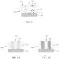
Classifications
-
- C—CHEMISTRY; METALLURGY
- C23—COATING METALLIC MATERIAL; COATING MATERIAL WITH METALLIC MATERIAL; CHEMICAL SURFACE TREATMENT; DIFFUSION TREATMENT OF METALLIC MATERIAL; COATING BY VACUUM EVAPORATION, BY SPUTTERING, BY ION IMPLANTATION OR BY CHEMICAL VAPOUR DEPOSITION, IN GENERAL; INHIBITING CORROSION OF METALLIC MATERIAL OR INCRUSTATION IN GENERAL
- C23C—COATING METALLIC MATERIAL; COATING MATERIAL WITH METALLIC MATERIAL; SURFACE TREATMENT OF METALLIC MATERIAL BY DIFFUSION INTO THE SURFACE, BY CHEMICAL CONVERSION OR SUBSTITUTION; COATING BY VACUUM EVAPORATION, BY SPUTTERING, BY ION IMPLANTATION OR BY CHEMICAL VAPOUR DEPOSITION, IN GENERAL
- C23C16/00—Chemical coating by decomposition of gaseous compounds, without leaving reaction products of surface material in the coating, i.e. chemical vapour deposition [CVD] processes
- C23C16/22—Chemical coating by decomposition of gaseous compounds, without leaving reaction products of surface material in the coating, i.e. chemical vapour deposition [CVD] processes characterised by the deposition of inorganic material, other than metallic material
- C23C16/30—Deposition of compounds, mixtures or solid solutions, e.g. borides, carbides, nitrides
- C23C16/34—Nitrides
- C23C16/345—Silicon nitride
-
- H—ELECTRICITY
- H10—SEMICONDUCTOR DEVICES; ELECTRIC SOLID-STATE DEVICES NOT OTHERWISE PROVIDED FOR
- H10P—GENERIC PROCESSES OR APPARATUS FOR THE MANUFACTURE OR TREATMENT OF DEVICES COVERED BY CLASS H10
- H10P14/00—Formation of materials, e.g. in the shape of layers or pillars
- H10P14/60—Formation of materials, e.g. in the shape of layers or pillars of insulating materials
- H10P14/66—Formation of materials, e.g. in the shape of layers or pillars of insulating materials characterised by the type of materials
- H10P14/668—Formation of materials, e.g. in the shape of layers or pillars of insulating materials characterised by the type of materials the materials being characterised by the deposition precursor materials
- H10P14/6681—Formation of materials, e.g. in the shape of layers or pillars of insulating materials characterised by the type of materials the materials being characterised by the deposition precursor materials the precursor containing a compound comprising Si
- H10P14/6687—Formation of materials, e.g. in the shape of layers or pillars of insulating materials characterised by the type of materials the materials being characterised by the deposition precursor materials the precursor containing a compound comprising Si the compound comprising silicon and nitrogen
-
- C—CHEMISTRY; METALLURGY
- C07—ORGANIC CHEMISTRY
- C07F—ACYCLIC, CARBOCYCLIC OR HETEROCYCLIC COMPOUNDS CONTAINING ELEMENTS OTHER THAN CARBON, HYDROGEN, HALOGEN, OXYGEN, NITROGEN, SULFUR, SELENIUM OR TELLURIUM
- C07F7/00—Compounds containing elements of Groups 4 or 14 of the Periodic Table
- C07F7/02—Silicon compounds
- C07F7/08—Compounds having one or more C—Si linkages
- C07F7/10—Compounds having one or more C—Si linkages containing nitrogen having a Si-N linkage
-
- C—CHEMISTRY; METALLURGY
- C23—COATING METALLIC MATERIAL; COATING MATERIAL WITH METALLIC MATERIAL; CHEMICAL SURFACE TREATMENT; DIFFUSION TREATMENT OF METALLIC MATERIAL; COATING BY VACUUM EVAPORATION, BY SPUTTERING, BY ION IMPLANTATION OR BY CHEMICAL VAPOUR DEPOSITION, IN GENERAL; INHIBITING CORROSION OF METALLIC MATERIAL OR INCRUSTATION IN GENERAL
- C23C—COATING METALLIC MATERIAL; COATING MATERIAL WITH METALLIC MATERIAL; SURFACE TREATMENT OF METALLIC MATERIAL BY DIFFUSION INTO THE SURFACE, BY CHEMICAL CONVERSION OR SUBSTITUTION; COATING BY VACUUM EVAPORATION, BY SPUTTERING, BY ION IMPLANTATION OR BY CHEMICAL VAPOUR DEPOSITION, IN GENERAL
- C23C16/00—Chemical coating by decomposition of gaseous compounds, without leaving reaction products of surface material in the coating, i.e. chemical vapour deposition [CVD] processes
- C23C16/04—Coating on selected surface areas, e.g. using masks
- C23C16/045—Coating cavities or hollow spaces, e.g. interior of tubes; Infiltration of porous substrates
-
- C—CHEMISTRY; METALLURGY
- C23—COATING METALLIC MATERIAL; COATING MATERIAL WITH METALLIC MATERIAL; CHEMICAL SURFACE TREATMENT; DIFFUSION TREATMENT OF METALLIC MATERIAL; COATING BY VACUUM EVAPORATION, BY SPUTTERING, BY ION IMPLANTATION OR BY CHEMICAL VAPOUR DEPOSITION, IN GENERAL; INHIBITING CORROSION OF METALLIC MATERIAL OR INCRUSTATION IN GENERAL
- C23C—COATING METALLIC MATERIAL; COATING MATERIAL WITH METALLIC MATERIAL; SURFACE TREATMENT OF METALLIC MATERIAL BY DIFFUSION INTO THE SURFACE, BY CHEMICAL CONVERSION OR SUBSTITUTION; COATING BY VACUUM EVAPORATION, BY SPUTTERING, BY ION IMPLANTATION OR BY CHEMICAL VAPOUR DEPOSITION, IN GENERAL
- C23C16/00—Chemical coating by decomposition of gaseous compounds, without leaving reaction products of surface material in the coating, i.e. chemical vapour deposition [CVD] processes
- C23C16/44—Chemical coating by decomposition of gaseous compounds, without leaving reaction products of surface material in the coating, i.e. chemical vapour deposition [CVD] processes characterised by the method of coating
- C23C16/448—Chemical coating by decomposition of gaseous compounds, without leaving reaction products of surface material in the coating, i.e. chemical vapour deposition [CVD] processes characterised by the method of coating characterised by the method used for generating reactive gas streams, e.g. by evaporation or sublimation of precursor materials
- C23C16/452—Chemical coating by decomposition of gaseous compounds, without leaving reaction products of surface material in the coating, i.e. chemical vapour deposition [CVD] processes characterised by the method of coating characterised by the method used for generating reactive gas streams, e.g. by evaporation or sublimation of precursor materials by activating reactive gas streams before their introduction into the reaction chamber, e.g. by ionisation or addition of reactive species
-
- C—CHEMISTRY; METALLURGY
- C23—COATING METALLIC MATERIAL; COATING MATERIAL WITH METALLIC MATERIAL; CHEMICAL SURFACE TREATMENT; DIFFUSION TREATMENT OF METALLIC MATERIAL; COATING BY VACUUM EVAPORATION, BY SPUTTERING, BY ION IMPLANTATION OR BY CHEMICAL VAPOUR DEPOSITION, IN GENERAL; INHIBITING CORROSION OF METALLIC MATERIAL OR INCRUSTATION IN GENERAL
- C23C—COATING METALLIC MATERIAL; COATING MATERIAL WITH METALLIC MATERIAL; SURFACE TREATMENT OF METALLIC MATERIAL BY DIFFUSION INTO THE SURFACE, BY CHEMICAL CONVERSION OR SUBSTITUTION; COATING BY VACUUM EVAPORATION, BY SPUTTERING, BY ION IMPLANTATION OR BY CHEMICAL VAPOUR DEPOSITION, IN GENERAL
- C23C16/00—Chemical coating by decomposition of gaseous compounds, without leaving reaction products of surface material in the coating, i.e. chemical vapour deposition [CVD] processes
- C23C16/44—Chemical coating by decomposition of gaseous compounds, without leaving reaction products of surface material in the coating, i.e. chemical vapour deposition [CVD] processes characterised by the method of coating
- C23C16/455—Chemical coating by decomposition of gaseous compounds, without leaving reaction products of surface material in the coating, i.e. chemical vapour deposition [CVD] processes characterised by the method of coating characterised by the method used for introducing gases into reaction chamber or for modifying gas flows in reaction chamber
- C23C16/45523—Pulsed gas flow or change of composition over time
-
- C—CHEMISTRY; METALLURGY
- C23—COATING METALLIC MATERIAL; COATING MATERIAL WITH METALLIC MATERIAL; CHEMICAL SURFACE TREATMENT; DIFFUSION TREATMENT OF METALLIC MATERIAL; COATING BY VACUUM EVAPORATION, BY SPUTTERING, BY ION IMPLANTATION OR BY CHEMICAL VAPOUR DEPOSITION, IN GENERAL; INHIBITING CORROSION OF METALLIC MATERIAL OR INCRUSTATION IN GENERAL
- C23C—COATING METALLIC MATERIAL; COATING MATERIAL WITH METALLIC MATERIAL; SURFACE TREATMENT OF METALLIC MATERIAL BY DIFFUSION INTO THE SURFACE, BY CHEMICAL CONVERSION OR SUBSTITUTION; COATING BY VACUUM EVAPORATION, BY SPUTTERING, BY ION IMPLANTATION OR BY CHEMICAL VAPOUR DEPOSITION, IN GENERAL
- C23C16/00—Chemical coating by decomposition of gaseous compounds, without leaving reaction products of surface material in the coating, i.e. chemical vapour deposition [CVD] processes
- C23C16/44—Chemical coating by decomposition of gaseous compounds, without leaving reaction products of surface material in the coating, i.e. chemical vapour deposition [CVD] processes characterised by the method of coating
- C23C16/50—Chemical coating by decomposition of gaseous compounds, without leaving reaction products of surface material in the coating, i.e. chemical vapour deposition [CVD] processes characterised by the method of coating using electric discharges
-
- C—CHEMISTRY; METALLURGY
- C23—COATING METALLIC MATERIAL; COATING MATERIAL WITH METALLIC MATERIAL; CHEMICAL SURFACE TREATMENT; DIFFUSION TREATMENT OF METALLIC MATERIAL; COATING BY VACUUM EVAPORATION, BY SPUTTERING, BY ION IMPLANTATION OR BY CHEMICAL VAPOUR DEPOSITION, IN GENERAL; INHIBITING CORROSION OF METALLIC MATERIAL OR INCRUSTATION IN GENERAL
- C23C—COATING METALLIC MATERIAL; COATING MATERIAL WITH METALLIC MATERIAL; SURFACE TREATMENT OF METALLIC MATERIAL BY DIFFUSION INTO THE SURFACE, BY CHEMICAL CONVERSION OR SUBSTITUTION; COATING BY VACUUM EVAPORATION, BY SPUTTERING, BY ION IMPLANTATION OR BY CHEMICAL VAPOUR DEPOSITION, IN GENERAL
- C23C16/00—Chemical coating by decomposition of gaseous compounds, without leaving reaction products of surface material in the coating, i.e. chemical vapour deposition [CVD] processes
- C23C16/44—Chemical coating by decomposition of gaseous compounds, without leaving reaction products of surface material in the coating, i.e. chemical vapour deposition [CVD] processes characterised by the method of coating
- C23C16/50—Chemical coating by decomposition of gaseous compounds, without leaving reaction products of surface material in the coating, i.e. chemical vapour deposition [CVD] processes characterised by the method of coating using electric discharges
- C23C16/505—Chemical coating by decomposition of gaseous compounds, without leaving reaction products of surface material in the coating, i.e. chemical vapour deposition [CVD] processes characterised by the method of coating using electric discharges using radio frequency discharges
-
- C—CHEMISTRY; METALLURGY
- C23—COATING METALLIC MATERIAL; COATING MATERIAL WITH METALLIC MATERIAL; CHEMICAL SURFACE TREATMENT; DIFFUSION TREATMENT OF METALLIC MATERIAL; COATING BY VACUUM EVAPORATION, BY SPUTTERING, BY ION IMPLANTATION OR BY CHEMICAL VAPOUR DEPOSITION, IN GENERAL; INHIBITING CORROSION OF METALLIC MATERIAL OR INCRUSTATION IN GENERAL
- C23C—COATING METALLIC MATERIAL; COATING MATERIAL WITH METALLIC MATERIAL; SURFACE TREATMENT OF METALLIC MATERIAL BY DIFFUSION INTO THE SURFACE, BY CHEMICAL CONVERSION OR SUBSTITUTION; COATING BY VACUUM EVAPORATION, BY SPUTTERING, BY ION IMPLANTATION OR BY CHEMICAL VAPOUR DEPOSITION, IN GENERAL
- C23C16/00—Chemical coating by decomposition of gaseous compounds, without leaving reaction products of surface material in the coating, i.e. chemical vapour deposition [CVD] processes
- C23C16/56—After-treatment
-
- H—ELECTRICITY
- H10—SEMICONDUCTOR DEVICES; ELECTRIC SOLID-STATE DEVICES NOT OTHERWISE PROVIDED FOR
- H10P—GENERIC PROCESSES OR APPARATUS FOR THE MANUFACTURE OR TREATMENT OF DEVICES COVERED BY CLASS H10
- H10P14/00—Formation of materials, e.g. in the shape of layers or pillars
- H10P14/60—Formation of materials, e.g. in the shape of layers or pillars of insulating materials
- H10P14/63—Formation of materials, e.g. in the shape of layers or pillars of insulating materials characterised by the formation processes
- H10P14/6326—Deposition processes
- H10P14/6328—Deposition from the gas or vapour phase
- H10P14/6334—Deposition from the gas or vapour phase using decomposition or reaction of gaseous or vapour phase compounds, i.e. chemical vapour deposition
- H10P14/6336—Deposition from the gas or vapour phase using decomposition or reaction of gaseous or vapour phase compounds, i.e. chemical vapour deposition in the presence of a plasma [PECVD]
-
- H—ELECTRICITY
- H10—SEMICONDUCTOR DEVICES; ELECTRIC SOLID-STATE DEVICES NOT OTHERWISE PROVIDED FOR
- H10P—GENERIC PROCESSES OR APPARATUS FOR THE MANUFACTURE OR TREATMENT OF DEVICES COVERED BY CLASS H10
- H10P14/00—Formation of materials, e.g. in the shape of layers or pillars
- H10P14/60—Formation of materials, e.g. in the shape of layers or pillars of insulating materials
- H10P14/66—Formation of materials, e.g. in the shape of layers or pillars of insulating materials characterised by the type of materials
- H10P14/668—Formation of materials, e.g. in the shape of layers or pillars of insulating materials characterised by the type of materials the materials being characterised by the deposition precursor materials
- H10P14/6681—Formation of materials, e.g. in the shape of layers or pillars of insulating materials characterised by the type of materials the materials being characterised by the deposition precursor materials the precursor containing a compound comprising Si
- H10P14/6687—Formation of materials, e.g. in the shape of layers or pillars of insulating materials characterised by the type of materials the materials being characterised by the deposition precursor materials the precursor containing a compound comprising Si the compound comprising silicon and nitrogen
- H10P14/6689—Formation of materials, e.g. in the shape of layers or pillars of insulating materials characterised by the type of materials the materials being characterised by the deposition precursor materials the precursor containing a compound comprising Si the compound comprising silicon and nitrogen the compound being a silazane
-
- H—ELECTRICITY
- H10—SEMICONDUCTOR DEVICES; ELECTRIC SOLID-STATE DEVICES NOT OTHERWISE PROVIDED FOR
- H10P—GENERIC PROCESSES OR APPARATUS FOR THE MANUFACTURE OR TREATMENT OF DEVICES COVERED BY CLASS H10
- H10P14/00—Formation of materials, e.g. in the shape of layers or pillars
- H10P14/60—Formation of materials, e.g. in the shape of layers or pillars of insulating materials
- H10P14/69—Inorganic materials
- H10P14/694—Inorganic materials composed of nitrides
- H10P14/6943—Inorganic materials composed of nitrides containing silicon
- H10P14/69433—Inorganic materials composed of nitrides containing silicon the material being a silicon nitride not containing oxygen, e.g. SixNy or SixByNz
Definitions
- the present disclosure relates generally to methods of depositing thin films.
- the disclosure relates to processes for depositing silicon nitride films with high nitrogen content.
- CVD chemical vapor deposition
- FCVD Flowable chemical vapor deposition
- SiN flowable films are commonly utilized for gap fill applications.
- TSA trisilylamine
- the as-deposited films obtained from the TSA process comprise Si and N as major components. These films usually have nitrogen to silicon ratios in the rage of 0.4:1 to 0.7:1. Films with higher nitrogen content may be useful in patterning applications to solve etch selectivity problems.
- One or more embodiments of the disclosure are directed to a method of depositing a SiN film.
- the method comprises exposing a substrate to a silicon-nitrogen precursor and a NH 3 plasma to deposit a flowable SiN polymer, and curing the flowable SiN polymner to form a cured SiN film.
- the silicon-nitrogen precursor comprises one or more of: where R 1 - R 5 are independently H or C1-C4 alkyl.
- Additional embodiments of the disclosure are directed to a method of depositing a SiN film.
- the method comprises exposing a substrate maintained at less than or equal to 25 °C to a silicon-nitrogen precursor and an NH 3 plasma to deposit a flowable SiN polymer, and curing the flowable SiN polymer to form a cured SiN film, where a ratio of nitrogen to silicon atoms in the cured SiN film is greater than about 1.0.
- the silicon-nitrogen precursor comprises one or more of: where R 1 - R 5 are independently H or methyl, with the proviso that at least one of R 1 -R 5 is methyl.
- a cured SiN film formed by exposing a substrate to a silicon-nitrogen precursor and an NH 3 plasma at a temperature less than or equal to about 25 °C without a UV light cure.
- a ratio of nitrogen to silicon atoms in the cured SiN film is in the range of about 1.0 to about 1.5 and the silicon nitrogen precursor comprises one or more of: where R 1 - R 5 are independently H or C1-C4 alkyl.
- substrate refers to a surface, or portion of a surface, upon which a process acts. It will also be understood by those skilled in the art that reference to a substrate can also refer to only a portion of the substrate, unless the context clearly indicates otherwise. Additionally, reference to depositing on a substrate can mean both a bare substrate and a substrate with one or more films or features deposited or formed thereon
- a “substrate” as used herein, refers to any substrate or material surface formed on a substrate upon which film processing is performed during a fabrication process.
- a substrate surface on which processing can be performed include materials such as silicon, silicon oxide, strained silicon, silicon on insulator (SOI), carbon doped silicon oxides, amorphous silicon, doped silicon, germanium, gallium arsenide, glass, sapphire, and any other materials such as metals, metal nitrides, metal alloys, and other conductive materials, depending on the application.
- Substrates include, without limitation, semiconductor wafers.
- Substrates may be exposed to a pretreatment process to polish, etch, reduce, oxidize, hydroxylate, anneal, UV cure, e-beam cure and/or bake the substrate surface.
- any of the film processing steps disclosed may also be performed on an underlayer formed on the substrate as disclosed in more detail below, and the term "substrate surface" is intended to include such underlayer as the context indicates.
- the exposed surface of the newly deposited film/layer becomes the substrate surface.
- One or more embodiments of the disclosure are directed to methods of depositing a silicon nitride film through the use of novel silicon-nitrogen precursors.
- Embodiments of this disclosure utilize a variety of CVD processes.
- a plasma-enhanced CVD (PECVD) process is used.
- a PECVD process is similar to CVD processes commonly known in the art with one or more reactants supplied as a plasma. Without being bound by theory, a PECVD process makes use of radicals present in the plasma reactant to facilitate reactions which would be otherwise unavailable through conventional thermal reactions.
- a flowable CVD (FCVD) process is used.
- FCVD process is similar to CVD processes commonly known in the art except that the deposited material is "flowable" such that it moves along the surface of the substrate to fill substrate features.
- the flowable materials deposited in an FCVD process are typically cured to solidify the flowable materials into a cured film which is no longer capable of moving along the substrate surface.
- the film deposition process comprises exposing a substrate to a silicon-nitrogen precursor and NH 3 plasma to deposit a flowable SiN polymer.
- the flowable polymer is cured to form a cured SiN film.
- FIG. 1 shows a cross-sectional view of a substrate 100 with two features 110 (e.g. trenches or vias).
- the number of features in the Figures is merely for illustrative purposes and should not be taken as limiting the scope of the disclosure. Those skilled in the art will understand that there can be no features or any number of features.
- the shape of the feature 110 can be any suitable shape including, but not limited to, trenches and cylindrical vias.
- the term "feature” means any intentional surface irregularity having an aspect ratio greater than or equal to about 2:1.
- the aspect ratio of a feature is the ratio of the depth D of the feature relative to the width W of the feature. A higher aspect ratio feature will have a narrower/longer shape than a lower aspect ratio feature.
- the features have an aspect ratio greater than or equal to about 3:1, 4:1, 5:1, 6:1, 7:1, 8:1, 9:1, 10:1, 15:1, 20:1, 25:1 or 30:1.
- trenches have a top, two sidewalls extending down from a surface to a bottom. As illustrated, each sidewall can be substantially orthogonal to the bottom or can be slanted relative to bottom at an angle other than 90 degrees, so that the opening at the surface is greater than at lower portion of the feature.
- the substrate 100 may be comprised of two materials; a first material 120 and a second material 130.
- the first material 120 and the second material 130 are the same material so that the feature 110 is bounded on the sides and bottom by the same material.
- the first material 120 and the second material 130 are different so that the bottom 115 of the feature is a different material than the sidewalls 111, 112 of the feature 110.
- the feature 110 extends into the substrate 100 a distance D from the substrate surface 125 to a bottom 115.
- the feature 110 has a first sidewall 111 and a second sidewall 112 that define a width W of the feature 110.
- the open area formed by the sidewalls and bottom are also referred to as a gap. Materials which fill the gap are referred to as gapfill.
- one or more embodiments of the disclosure are directed to film deposition processes that utilize a silicon-nitrogen precursor and a plasma (e.g., ammonia).
- a silicon-nitrogen precursor and a plasma e.g., ammonia
- the silicon-nitrogen precursor and plasma reactants are flowed simultaneously into the processing chamber.
- the silicon-nitrogen precursor and plasma can be mixed in the processing chamber or before entering the processing chamber.
- these reactants are flowed sequentially into the processing chamber to avoid gas phase mixing of the precursor and plasma reactants.
- the silicon-nitrogen precursor comprises a compound having the general formula (I) where each of the R substituents (R 1 - R 5 ) is independently selected from H or C1-C4 alkyl.
- C1-C4 alkyl means any group with 1-4 carbon atoms.
- Examples of C1-C4 alkyl groups include, but are not limited to, methyl, ethyl, propyl, isopropyl, butyl, isobutyl, sec-butyl and t-butyl groups.
- all of the R groups are the same.
- at least one of the R substituents is a methyl group.
- At least one of the R groups is not a hydrogen atom. In some embodiments, at least one of the R groups comprises an ethyl group, a propyl group, an isopropyl group, a butyl group, an isobutyl group, a sec-butyl group or a t-butyl group.
- the silicon-nitrogen precursor consists essentially of a compound of Formula (I) where each R 1 - R 5 are independently H or C1-C4 alkyl.
- the term "consists essentially of” means that the reactive species in the silicon-nitrogen precursor is greater than or equal to about 95% of the designated species, on a molar basis.
- the silicon-nitrogen precursor comprises one or more of:
- the silicon-nitrogen precursor comprises a compound having the general formula (II) where each of the R substituents (R 1 - R 5 ) is independently selected from H or C1-C4 alkyl.
- C1-C4 alkyl groups include, but are not limited to, methyl, ethyl, propyl, isopropyl, butyl, isobutyl, sec-butyl and t-butyl groups.
- all of the R groups are the same.
- at least one of the R substituents is a methyl group.
- at least one of the R groups is not a hydrogen atom.
- At least one of the R groups comprises an ethyl group, a propyl group, an isopropyl group, a butyl group, an isobutyl group, a sec-butyl group or a t-butyl group.
- the silicon-nitrogen precursor consists essentially of a compound of Formula (II) where each R 1 - R 5 are independently H or C1-C4 alkyl. In some embodiments, the silicon-nitrogen precursor comprises one or more of:
- the silicon-nitrogen precursor comprises a compound having the general formula (III) where each of the R substituents (R 1 - R 2 ) is independently selected from H or C1-C4 alkyl.
- C1-C4 alkyl groups include, but are not limited to, methyl, ethyl, propyl, isopropyl, butyl, isobutyl, sec-butyl and t-butyl groups.
- all of the R groups are the same.
- at least one of the R substituents is a methyl group.
- at least one of the R groups is not a hydrogen atom.
- At least one of the R groups comprises an ethyl group, a propyl group, an isopropyl group, a butyl group, an isobutyl group, a sec-butyl group or a t-butyl group.
- the silicon nitrogen precursor consists essentially of a compound of Formula (III) where R 1 - R 2 are independently H or C1-C4 alkyl.
- the silicon-nitrogen precursor comprises one or more of:
- the silicon-nitrogen precursor may be provided in one or more pulses or continuously.
- the flow rate of the precursor can be any suitable flow rate including, but not limited to, flow rates is in the range of about 1 to about 1000 sccm, or in the range of about 2 to about 500 sccm, or in the range of about 3 to about 200 sccm or in the range of about 5 to about 100 sccm or in the range of about 10 to about 50 sccm or in the range of about 15 to 25 sccm.
- the flow rate of the precursor is less than or equal to about 50 sccm, 45 sccm, 40 sccm, 35 sccm, 30 sccm, 25 sccm, 20 sccm or 15 sccm.
- the precursor can be provided at any suitable pressure including, but not limited to, a pressure in the range of about 5 mTorr to about 25 Torr, or in the range of about 100 mTorr to about 20 Torr, or in the range of about 5 Torr to about 20 Torr, or in the range of about 50 mTorr to about 2000 mTorr, or in the range of about 100 mTorr to about 1000 mTorr, or in the range of about 200 mTorr to about 500 mTorr.
- a pressure in the range of about 5 mTorr to about 25 Torr, or in the range of about 100 mTorr to about 20 Torr, or in the range of about 5 Torr to about 20 Torr, or in the range of about 50 mTorr to about 2000 mTorr, or in the range of about 100 mTorr to about 1000 mTorr, or in the range of about 200 mTorr to about 500 mTorr.
- a “pulse” or “dose” as used herein is intended to refer to a quantity of a reactant that is intermittently or non-continuously introduced into the process chamber.
- the quantity of a particular compound within each pulse may vary over time, depending on the duration of the pulse.
- Any particular reactant may include a single compound or a mixture/combination of two or more compounds.
- the durations for each pulse/dose are variable and may be adjusted to accommodate, for example, the volume capacity of the processing chamber as well as the capabilities of a vacuum system coupled thereto. Additionally, the dose time of a reactant may vary according to the flow rate of the reactant, the temperature of the reactant, the type of control valve, the type of process chamber employed, as well as the ability of the components of the reactant to react and form a suitable film. Dose times may also vary based upon the type of film being formed and the geometry of the substrate. A dose time should be long enough to provide a volume of reactant sufficient to adsorb/chemisorb onto substantially the entire surface of the substrate and form a layer of reactive species thereon.
- the reactant comprises an inert, diluent and/or carrier gas.
- the inert, diluent and/or carrier gas may be mixed with the reactive species and can be pulsed or have a constant flow.
- the carrier gas is flowed into the processing chamber at a constant flow in the range of about 1 to about 20000 sccm.
- the carrier gas may be any gas which does not interfere with the film deposition.
- the carrier gas may comprises one or more of argon, helium, hydrogen, nitrogen, neon, or the like, or combinations thereof.
- the carrier gas is mixed with the reactive species prior to flowing into the process chamber.
- the ammonia plasma can be generated at any suitable location.
- the plasma can be generated or ignited within the processing chamber (e.g., a direct plasma) or can be generated outside of the processing chamber and flowed into the processing chamber (e.g., a remote plasma).
- the plasma is generated external from the processing chamber, such as by a remote plasma source.
- remote plasma generation can occur upstream of the deposition chamber such that reactive species are in direct contact with the deposited film.
- the plasma is described with respect to an ammonia plasma.
- the plasma can have different reactive species than ammonia.
- the plasma can include nitrogen or hydrazine.
- the ammonia plasma may be generated via any suitable plasma generation process or technique known to those skilled in the art.
- plasma may be generated by one or more of a microwave (MW) frequency generator or a radio frequency (RF) generator.
- MW microwave
- RF radio frequency
- the frequency of the plasma may be tuned depending on the specific reactive species being used. Suitable frequencies include, but are not limited to, 2 MHz, 13.56 MHz, 40 MHz, 60 MHz and 100 MHz.
- the NH 3 plasma is generated using a remote plasma source.
- the plasma power is less than or equal to about 300 W. In one or more embodiments, the plasma power is less than or equal to about 250 W, 200 W, 150 W, 100 W, 50 W or 25 W. In some embodiments, the plasma power is in the range of about 10 W to about 200 W, or in the range of about 25 W to about 175 W, or in the range of about 50 W to about 150 W.
- the plasma is generated in a remote plasma source and flowed to the processing region of a processing chamber so that the radicals present in the plasma can react with the silicon-nitrogen precursor or the substrate or film on the substrate.
- the remote plasma is configured so that there is a greater number of radicals than ions in the processing region of the processing chamber.
- the NH 3 radicals are generated using a hot wire in place of or in addition to the plasma source.
- the term "hotwire" means any element that can be heated to a temperature sufficient to generate radicals in a fluid flowing across the element.
- the hotwire is one or more metallic filaments (e.g., tungsten).
- the hotwire is a filament comprising one or more of tungsten, tantalum or ruthenium.
- the filament temperature is maintained in the range of about 200 °C to about 1500 °C or in the range of about 1000 °C to about 1500 °C or in the range of 1100 °C to about 1400 °C.
- the filament temperature is maintained at a temperature less than about 1500 °C, 1400 °C, 1300 °C or 1200 °C.
- the substrate is maintained at a cool temperature (i.e., less than or equal to about 25 °C).
- the substrate 100 temperature can be controlled.
- the substrate 100 is cooled to a temperature less than or equal to about 25 °C.
- Such cooling can be accomplished by any suitable means including, but not limited to, changing the temperature of the substrate support or flowing cooled gases to the substrate surface.
- the substrate support includes a chiller which can be controlled to change the substrate temperature conductively.
- the gases (including reactants and/or carrier gases) being employed are cooled to locally change the substrate temperature.
- a chiller is positioned within the chamber adjacent the substrate surface to convectively change the substrate temperature.
- the substrate 100 is exposed to the silicon-nitrogen precursor and the reactant to form a flowable film 210 on the substrate.
- the flowable film 210 illustrated in FIG. 2A is only in the features; however, those skilled in the art will understand that this is merely for descriptive purposes.
- the flowable film 210 can be deposited on a substrate maintained at any suitable temperature.
- the substrate is maintained at a temperature in the range of about -100 °C to about 25 °C, or in the range of about -75 °C to about 20 °C, or in the range of about -50 °C to about 10 °C, or in the range of about -25 °C to about 0 °C.
- the temperature is kept low to promote the polymerization of the silicon nitrogen precursors.
- the substrate is maintained at a temperature less than about 25 °C, 20 °C, 15 °C, 10 °C, 5 °C, 0 °C, -10 °C, -20 °C, -30 °C, -40 °C, -50 °C, -60 °C, -70 °C, -80 °C or -90 °C.
- the flowable film 210 can be formed at any suitable pressure.
- the pressure used for formation of the flowable film 210 is in the range of about 0.5 T to about 50 T, or in the range of about 0.75 T to about 25 T, or in the range of about 1 T to about 10 T, or in the range of about 2 T to about 8 T, or in the range of about 3 T to about 6 T.
- the flowable film 210 is cured to form a cured film 220.
- the flowable film 210 can be cured by any suitable means.
- the flowable film 210 is cured by exposure to the radicals within the plasma or from the hotwire.
- the flowable film 210 is cured by exposure to ultraviolet (UV) radiation.
- UV radiation ultraviolet
- the flowable film 210 is cured without the use of UV radiation.
- the flowable film 210 is cured substantially only by radical exposure.
- the term "cured substantially only by radical exposure" means that greater than or equal to about 90%, 95%, 98% or 99% of the flowable film 210 is cured using radicals.
- the cured film is subjected to a post-deposition treatment process.
- the post-deposition treatment process comprises at least one process to polish, etch, reduce, oxidize, hydroxylate, anneal, UV cure, e-beam cure or bake the substrate surface or any deposited film.
- a cured film 220 is formed on the substrate 100.
- a partial film of gapfill forms along the sidewalls 111, 112 and the bottom 115.
- the potential exists for the formation of a seam if the top of the gap closes before the bottom is filled with gapfill material. Seam formation is more likely to occur in higher aspect ratio features as the film at the top of the feature tends to pinch close so that a void is enclosed within the deposited gapfill.
- the term "seam” means any space or void between the sidewalls 111, 112 where the volume of the void volume is greater than 1% of the volume of the gap or other feature.
- the cured SiN film deposited is substantially free of seams.
- the cured film of the disclosed embodiments has a higher ratio of nitrogen atoms to silicon atoms.
- the cured SiN film has a ratio of nitrogen atoms to silicon atoms of greater than or equal to about 0.7, 0.8, 0.9, or 1.0.
- the cured SiN film has a ratio of nitrogen atoms to silicon atoms is in the range with a lower end of about 1.0, 1.1, 1.2 or 1.33 to an upper end of about 1.33, 1.4 or 1.5.
- the cured SiN film contains substantially no carbon atoms.
- substantially no carbon atoms means that carbon atoms make up less than or equal to about 5%, 2% or 1% of the atoms in the cured film on an atomic basis.
Landscapes
- Chemical & Material Sciences (AREA)
- Engineering & Computer Science (AREA)
- Organic Chemistry (AREA)
- Metallurgy (AREA)
- Materials Engineering (AREA)
- Mechanical Engineering (AREA)
- Chemical Kinetics & Catalysis (AREA)
- General Chemical & Material Sciences (AREA)
- Physics & Mathematics (AREA)
- Plasma & Fusion (AREA)
- Inorganic Chemistry (AREA)
- Chemical Vapour Deposition (AREA)
- Formation Of Insulating Films (AREA)
Abstract
Description
- The present disclosure relates generally to methods of depositing thin films. In particular, the disclosure relates to processes for depositing silicon nitride films with high nitrogen content.
- Deposition of thin films on a substrate surface is an important process in a variety of industries including semiconductor processing, diffusion barrier coatings and dielectrics for magnetic read/write heads. In the semiconductor industry, in particular, miniaturization benefits from a high level control of thin film deposition to produce conformal coatings on high aspect structures. One method for deposition of thin films with relative control and conformal deposition is chemical vapor deposition (CVD). CVD involves exposing a substrate (e.g., a wafer) to one or more precursors, which react to deposit a film onto the substrate. Flowable chemical vapor deposition (FCVD) is a type of CVD that allows for the deposition of flowable films, in particular for gap fill applications.
- SiN flowable films are commonly utilized for gap fill applications. Currently, such films are generated by trisilylamine (TSA) with radical forms of NH3 as coreactants. The as-deposited films obtained from the TSA process comprise Si and N as major components. These films usually have nitrogen to silicon ratios in the rage of 0.4:1 to 0.7:1. Films with higher nitrogen content may be useful in patterning applications to solve etch selectivity problems.
- Therefore, there is a need for new deposition chemistries that allow the deposition of SiN films with higher nitrogen content.
- One or more embodiments of the disclosure are directed to a method of depositing a SiN film. The method comprises exposing a substrate to a silicon-nitrogen precursor and a NH3 plasma to deposit a flowable SiN polymer, and curing the flowable SiN polymner to form a cured SiN film. In these embodiments, the silicon-nitrogen precursor comprises one or more of:

- Additional embodiments of the disclosure are directed to a method of depositing a SiN film. The method comprises exposing a substrate maintained at less than or equal to 25 °C to a silicon-nitrogen precursor and an NH3 plasma to deposit a flowable SiN polymer, and curing the flowable SiN polymer to form a cured SiN film, where a ratio of nitrogen to silicon atoms in the cured SiN film is greater than about 1.0. In these embodiments, the silicon-nitrogen precursor comprises one or more of:

- Further embodiments of the disclosure are directed to a cured SiN film formed by exposing a substrate to a silicon-nitrogen precursor and an NH3 plasma at a temperature less than or equal to about 25 °C without a UV light cure. In these embodiments, a ratio of nitrogen to silicon atoms in the cured SiN film is in the range of about 1.0 to about 1.5 and the silicon nitrogen precursor comprises one or more of:

- So that the manner in which the above recited features of the present invention can be understood in detail, a more particular description of the invention, briefly summarized above, may be had by reference to embodiments, some of which are illustrated in the appended drawings. It is to be noted, however, that the appended drawings illustrate only typical embodiments of this invention and are therefore not to be considered limiting of its scope, for the invention may admit to other equally effective embodiments.
-
FIG. 1 shows a cross-sectional schematic of a substrate in accordance with one or more embodiment of the disclosure; -
FIG. 2A shows the deposition of a flowable film in accordance with one or more embodiments of the disclosure; and -
FIG. 2B shows the formation of a cured film in accordance with one or more embodiment of the disclosure. - Before describing several exemplary embodiments of the invention, it is to be understood that the invention is not limited to the details of construction or process steps set forth in the following description. The invention is capable of other embodiments and of being practiced or being carried out in various ways.
- As used in this specification and the appended claims, the term "substrate" refers to a surface, or portion of a surface, upon which a process acts. It will also be understood by those skilled in the art that reference to a substrate can also refer to only a portion of the substrate, unless the context clearly indicates otherwise. Additionally, reference to depositing on a substrate can mean both a bare substrate and a substrate with one or more films or features deposited or formed thereon
- A "substrate" as used herein, refers to any substrate or material surface formed on a substrate upon which film processing is performed during a fabrication process. For example, a substrate surface on which processing can be performed include materials such as silicon, silicon oxide, strained silicon, silicon on insulator (SOI), carbon doped silicon oxides, amorphous silicon, doped silicon, germanium, gallium arsenide, glass, sapphire, and any other materials such as metals, metal nitrides, metal alloys, and other conductive materials, depending on the application. Substrates include, without limitation, semiconductor wafers. Substrates may be exposed to a pretreatment process to polish, etch, reduce, oxidize, hydroxylate, anneal, UV cure, e-beam cure and/or bake the substrate surface. In addition to film processing directly on the surface of the substrate itself, in the present invention, any of the film processing steps disclosed may also be performed on an underlayer formed on the substrate as disclosed in more detail below, and the term "substrate surface" is intended to include such underlayer as the context indicates. Thus for example, where a film/layer or partial film/layer has been deposited onto a substrate surface, the exposed surface of the newly deposited film/layer becomes the substrate surface.
- One or more embodiments of the disclosure are directed to methods of depositing a silicon nitride film through the use of novel silicon-nitrogen precursors. Embodiments of this disclosure utilize a variety of CVD processes. In some embodiments, a plasma-enhanced CVD (PECVD) process is used. A PECVD process is similar to CVD processes commonly known in the art with one or more reactants supplied as a plasma. Without being bound by theory, a PECVD process makes use of radicals present in the plasma reactant to facilitate reactions which would be otherwise unavailable through conventional thermal reactions. In some embodiments, a flowable CVD (FCVD) process is used. An FCVD process is similar to CVD processes commonly known in the art except that the deposited material is "flowable" such that it moves along the surface of the substrate to fill substrate features. The flowable materials deposited in an FCVD process are typically cured to solidify the flowable materials into a cured film which is no longer capable of moving along the substrate surface.
- In some embodiments, the film deposition process comprises exposing a substrate to a silicon-nitrogen precursor and NH3 plasma to deposit a flowable SiN polymer. The flowable polymer is cured to form a cured SiN film.
-
FIG. 1 shows a cross-sectional view of asubstrate 100 with two features 110 (e.g. trenches or vias). The number of features in the Figures is merely for illustrative purposes and should not be taken as limiting the scope of the disclosure. Those skilled in the art will understand that there can be no features or any number of features. The shape of thefeature 110 can be any suitable shape including, but not limited to, trenches and cylindrical vias. As used in this regard, the term "feature" means any intentional surface irregularity having an aspect ratio greater than or equal to about 2:1. The aspect ratio of a feature is the ratio of the depth D of the feature relative to the width W of the feature. A higher aspect ratio feature will have a narrower/longer shape than a lower aspect ratio feature. In some embodiments, the features have an aspect ratio greater than or equal to about 3:1, 4:1, 5:1, 6:1, 7:1, 8:1, 9:1, 10:1, 15:1, 20:1, 25:1 or 30:1. For purposes of this disclosure, trenches have a top, two sidewalls extending down from a surface to a bottom. As illustrated, each sidewall can be substantially orthogonal to the bottom or can be slanted relative to bottom at an angle other than 90 degrees, so that the opening at the surface is greater than at lower portion of the feature. - Referring to
FIG. 1 , thesubstrate 100 may be comprised of two materials; afirst material 120 and asecond material 130. In some embodiments, thefirst material 120 and thesecond material 130 are the same material so that thefeature 110 is bounded on the sides and bottom by the same material. In some embodiments, thefirst material 120 and thesecond material 130 are different so that thebottom 115 of the feature is a different material than thesidewalls feature 110. - The
feature 110 extends into the substrate 100 a distance D from thesubstrate surface 125 to a bottom 115. Thefeature 110 has afirst sidewall 111 and asecond sidewall 112 that define a width W of thefeature 110. The open area formed by the sidewalls and bottom are also referred to as a gap. Materials which fill the gap are referred to as gapfill. - Referring to
FIGS. 2A and 2B , one or more embodiments of the disclosure are directed to film deposition processes that utilize a silicon-nitrogen precursor and a plasma (e.g., ammonia). In some embodiments, the silicon-nitrogen precursor and plasma reactants are flowed simultaneously into the processing chamber. The silicon-nitrogen precursor and plasma can be mixed in the processing chamber or before entering the processing chamber. In some embodiments, these reactants are flowed sequentially into the processing chamber to avoid gas phase mixing of the precursor and plasma reactants. - In some embodiments, the silicon-nitrogen precursor comprises a compound having the general formula (I)

- In some embodiments, the silicon-nitrogen precursor consists essentially of a compound of Formula (I) where each R1 - R5 are independently H or C1-C4 alkyl. As used in this regard, the term "consists essentially of" means that the reactive species in the silicon-nitrogen precursor is greater than or equal to about 95% of the designated species, on a molar basis. In some embodiments, the silicon-nitrogen precursor comprises one or more of:


- In some embodiments, the silicon-nitrogen precursor comprises a compound having the general formula (II)

- In some embodiments, the silicon-nitrogen precursor consists essentially of a compound of Formula (II) where each R1 - R5 are independently H or C1-C4 alkyl. In some embodiments, the silicon-nitrogen precursor comprises one or more of:


- In some embodiments, the silicon-nitrogen precursor comprises a compound having the general formula (III)

- In some embodiments, the silicon nitrogen precursor consists essentially of a compound of Formula (III) where R1 - R2 are independently H or C1-C4 alkyl. In some embodiments, the silicon-nitrogen precursor comprises one or more of:

- The silicon-nitrogen precursor may be provided in one or more pulses or continuously. The flow rate of the precursor can be any suitable flow rate including, but not limited to, flow rates is in the range of about 1 to about 1000 sccm, or in the range of about 2 to about 500 sccm, or in the range of about 3 to about 200 sccm or in the range of about 5 to about 100 sccm or in the range of about 10 to about 50 sccm or in the range of about 15 to 25 sccm. In some embodiments, the flow rate of the precursor is less than or equal to about 50 sccm, 45 sccm, 40 sccm, 35 sccm, 30 sccm, 25 sccm, 20 sccm or 15 sccm. The precursor can be provided at any suitable pressure including, but not limited to, a pressure in the range of about 5 mTorr to about 25 Torr, or in the range of about 100 mTorr to about 20 Torr, or in the range of about 5 Torr to about 20 Torr, or in the range of about 50 mTorr to about 2000 mTorr, or in the range of about 100 mTorr to about 1000 mTorr, or in the range of about 200 mTorr to about 500 mTorr.
- A "pulse" or "dose" as used herein is intended to refer to a quantity of a reactant that is intermittently or non-continuously introduced into the process chamber. The quantity of a particular compound within each pulse may vary over time, depending on the duration of the pulse. Any particular reactant may include a single compound or a mixture/combination of two or more compounds.
- The durations for each pulse/dose are variable and may be adjusted to accommodate, for example, the volume capacity of the processing chamber as well as the capabilities of a vacuum system coupled thereto. Additionally, the dose time of a reactant may vary according to the flow rate of the reactant, the temperature of the reactant, the type of control valve, the type of process chamber employed, as well as the ability of the components of the reactant to react and form a suitable film. Dose times may also vary based upon the type of film being formed and the geometry of the substrate. A dose time should be long enough to provide a volume of reactant sufficient to adsorb/chemisorb onto substantially the entire surface of the substrate and form a layer of reactive species thereon.
- In some embodiments, the reactant comprises an inert, diluent and/or carrier gas. The inert, diluent and/or carrier gas may be mixed with the reactive species and can be pulsed or have a constant flow. In some embodiments, the carrier gas is flowed into the processing chamber at a constant flow in the range of about 1 to about 20000 sccm. The carrier gas may be any gas which does not interfere with the film deposition. For example the carrier gas may comprises one or more of argon, helium, hydrogen, nitrogen, neon, or the like, or combinations thereof. In one or more embodiments, the carrier gas is mixed with the reactive species prior to flowing into the process chamber.
- The ammonia plasma can be generated at any suitable location. The plasma can be generated or ignited within the processing chamber (e.g., a direct plasma) or can be generated outside of the processing chamber and flowed into the processing chamber (e.g., a remote plasma). In some embodiments, the plasma is generated external from the processing chamber, such as by a remote plasma source. In some embodiments, remote plasma generation can occur upstream of the deposition chamber such that reactive species are in direct contact with the deposited film.
- The plasma is described with respect to an ammonia plasma. However, those skilled in the art will understand that the plasma can have different reactive species than ammonia. For example, the plasma can include nitrogen or hydrazine. The ammonia plasma may be generated via any suitable plasma generation process or technique known to those skilled in the art. For example, plasma may be generated by one or more of a microwave (MW) frequency generator or a radio frequency (RF) generator. The frequency of the plasma may be tuned depending on the specific reactive species being used. Suitable frequencies include, but are not limited to, 2 MHz, 13.56 MHz, 40 MHz, 60 MHz and 100 MHz.
- In some embodiments, the NH3 plasma is generated using a remote plasma source. In some embodiments, the plasma power is less than or equal to about 300 W. In one or more embodiments, the plasma power is less than or equal to about 250 W, 200 W, 150 W, 100 W, 50 W or 25 W. In some embodiments, the plasma power is in the range of about 10 W to about 200 W, or in the range of about 25 W to about 175 W, or in the range of about 50 W to about 150 W.
- In some embodiments, the plasma is generated in a remote plasma source and flowed to the processing region of a processing chamber so that the radicals present in the plasma can react with the silicon-nitrogen precursor or the substrate or film on the substrate. In some embodiments, the remote plasma is configured so that there is a greater number of radicals than ions in the processing region of the processing chamber.
- In some embodiments, the NH3 radicals are generated using a hot wire in place of or in addition to the plasma source. As used in this specification and the appended claims, the term "hotwire" means any element that can be heated to a temperature sufficient to generate radicals in a fluid flowing across the element. In some embodiments, the hotwire is one or more metallic filaments (e.g., tungsten). In some embodiments, the hotwire is a filament comprising one or more of tungsten, tantalum or ruthenium. In some embodiments, the filament temperature is maintained in the range of about 200 °C to about 1500 °C or in the range of about 1000 °C to about 1500 °C or in the range of 1100 °C to about 1400 °C. In some embodiments, the filament temperature is maintained at a temperature less than about 1500 °C, 1400 °C, 1300 °C or 1200 °C. In embodiments in which a hotwire is employed to generate radical species, the substrate is maintained at a cool temperature (i.e., less than or equal to about 25 °C).
- During deposition, the
substrate 100 temperature can be controlled. In some embodiments, thesubstrate 100 is cooled to a temperature less than or equal to about 25 °C. Such cooling can be accomplished by any suitable means including, but not limited to, changing the temperature of the substrate support or flowing cooled gases to the substrate surface. In some embodiments, the substrate support includes a chiller which can be controlled to change the substrate temperature conductively. In one or more embodiments, the gases (including reactants and/or carrier gases) being employed are cooled to locally change the substrate temperature. In some embodiments, a chiller is positioned within the chamber adjacent the substrate surface to convectively change the substrate temperature. - Referring to
FIG. 2A , thesubstrate 100 is exposed to the silicon-nitrogen precursor and the reactant to form aflowable film 210 on the substrate. Theflowable film 210 illustrated inFIG. 2A is only in the features; however, those skilled in the art will understand that this is merely for descriptive purposes. - The
flowable film 210 can be deposited on a substrate maintained at any suitable temperature. In some embodiments, the substrate is maintained at a temperature in the range of about -100 °C to about 25 °C, or in the range of about -75 °C to about 20 °C, or in the range of about -50 °C to about 10 °C, or in the range of about -25 °C to about 0 °C. Without being bound by theory, the temperature is kept low to promote the polymerization of the silicon nitrogen precursors. In some embodiments, the substrate is maintained at a temperature less than about 25 °C, 20 °C, 15 °C, 10 °C, 5 °C, 0 °C, -10 °C, -20 °C, -30 °C, -40 °C, -50 °C, -60 °C, -70 °C, -80 °C or -90 °C. - The
flowable film 210 can be formed at any suitable pressure. In some embodiments, the pressure used for formation of theflowable film 210 is in the range of about 0.5 T to about 50 T, or in the range of about 0.75 T to about 25 T, or in the range of about 1 T to about 10 T, or in the range of about 2 T to about 8 T, or in the range of about 3 T to about 6 T. - Referring to
FIG. 2B , after deposition, theflowable film 210 is cured to form a curedfilm 220. Theflowable film 210 can be cured by any suitable means. In some embodiments, theflowable film 210 is cured by exposure to the radicals within the plasma or from the hotwire. In some embodiments, theflowable film 210 is cured by exposure to ultraviolet (UV) radiation. In some embodiments, theflowable film 210 is cured without the use of UV radiation. In some embodiments, theflowable film 210 is cured substantially only by radical exposure. As used in this specification and the appended claims, the term "cured substantially only by radical exposure" means that greater than or equal to about 90%, 95%, 98% or 99% of theflowable film 210 is cured using radicals. - In some embodiments, the cured film is subjected to a post-deposition treatment process. In some embodiments, the post-deposition treatment process comprises at least one process to polish, etch, reduce, oxidize, hydroxylate, anneal, UV cure, e-beam cure or bake the substrate surface or any deposited film.
- With reference to
FIG. 2B , a curedfilm 220 is formed on thesubstrate 100. Within the gap, a partial film of gapfill forms along thesidewalls sidewalls - The cured film of the disclosed embodiments has a higher ratio of nitrogen atoms to silicon atoms. In some embodiments, the cured SiN film has a ratio of nitrogen atoms to silicon atoms of greater than or equal to about 0.7, 0.8, 0.9, or 1.0. In some embodiments, the cured SiN film has a ratio of nitrogen atoms to silicon atoms is in the range with a lower end of about 1.0, 1.1, 1.2 or 1.33 to an upper end of about 1.33, 1.4 or 1.5. In some embodiments, the cured SiN film contains substantially no carbon atoms. As used in this regard, the term "substantially no carbon atoms" means that carbon atoms make up less than or equal to about 5%, 2% or 1% of the atoms in the cured film on an atomic basis.
- Reference throughout this specification to "one embodiment," "certain embodiments," "one or more embodiments" or "an embodiment" means that a particular feature, structure, material, or characteristic described in connection with the embodiment is included in at least one embodiment of the disclosure. Thus, the appearances of the phrases such as "in one or more embodiments," "in certain embodiments," "in one embodiment" or "in an embodiment" in various places throughout this specification are not necessarily referring to the same embodiment of the disclosure. Furthermore, the particular features, structures, materials, or characteristics may be combined in any suitable manner in one or more embodiments.
- Although the disclosure herein has been described with reference to particular embodiments, those skilled in the art will understand that the embodiments described are merely illustrative of the principles and applications of the present disclosure. It will be apparent to those skilled in the art that various modifications and variations can be made to the method and apparatus of the present disclosure without departing from the spirit and scope of the disclosure. Thus, the present disclosure can include modifications and variations that are within the scope of the appended claims and their equivalents.
The following items form part of the present invention: - 1. A method of depositing a SiN film, comprising:
- exposing a substrate to a silicon-nitrogen precursor and a NH3 plasma to deposit a flowable SiN polymer; and
- curing the flowable SiN polymer to form a cured SiN film;
- wherein the silicon-nitrogen precursor comprises one or more of:


- 2. The method of item 1, wherein at least one R group in the silicon-nitrogen precursor is a methyl group.
- 3. The method of item 1, wherein the silicon-nitrogen precursor comprises one or more of:


- 4. The method of item 1, wherein the silicon-nitrogen precursor consists essentially of

- 5. The method of item 4, wherein the silicon-nitrogen precursor comprises one or more of:

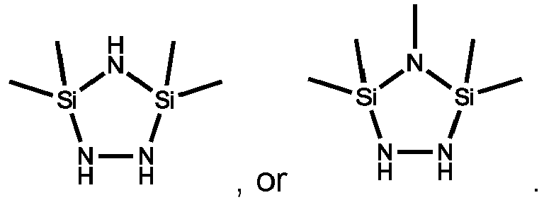
- 6. The method of item 1, wherein the silicon-nitrogen precursor consists essentially of

- 7. The method of item 6, wherein the silicon-nitrogen precursor comprises one or more of:

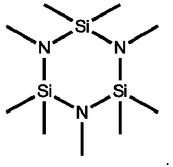
- 8. The method of item 1, wherein the silicon-nitrogen precursor consists essentially of

- 9. The method of item 8, wherein the silicon-nitrogen precursor comprises one or more of:

- 10. The method of any of items 1 to 9, wherein the plasma is generated using a remote plasma source.
- 11. The method of any of items 1 to 9, wherein the flowable SiN polymer is cured by exposure to radicals in the plasma.
- 12. The method of any of items 1 to 9, further comprising a post treatment comprising UV radiation exposure or annealing.
- 13. The method of any of items 1 to 9, wherein the cured SiN film has a ratio of nitrogen atoms to silicon atoms of greater than or equal to about 0.7.
- 14. The method of any of items 1 to 9, wherein the substrate is maintained at a temperature of less than or equal to about 25 °C.
- 15. A cured SiN film formed by exposing a substrate to a silicon-nitrogen precursor and an NH3 plasma at a temperature less than or equal to about 25 °C without a UV radiation cure, wherein a ratio of nitrogen to silicon atoms in the cured SiN film is in the range of about 1.0 to about 1.5 and the silicon nitrogen precursor comprises one or more of:


Claims (14)
- A method of depositing a SiN film, comprising:exposing a substrate to a silicon-nitrogen precursor and a NH3 plasma to deposit a flowable SiN polymer; andcuring the flowable SiN polymer to form a cured SiN film;wherein the silicon-nitrogen precursor comprises:


- The method of claim 1, wherein at least one R group in the silicon-nitrogen precursor is a methyl group.
- The method of claim 1, wherein the silicon-nitrogen precursor comprises: at least one of


- The method of claim 1, wherein the plasma is generated using a remote plasma source.
- The method of claim 1, wherein the flowable SiN polymer is cured by exposure to radicals in the plasma.
- The method of claim 1, further comprising a post-deposition treatment comprising UV radiation exposure or annealing.
- The method of claim 1, wherein the cured SiN film has a ratio of nitrogen atoms to silicon atoms of greater than or equal to 0.7.
- The method of claim 7, wherein the cured SiN film has a ratio of nitrogen atoms to silicon atoms of greater than or equal to 1.0.
- The method of claim 1, wherein the cured SiN film has a ratio of nitrogen atoms to silicon atoms is in the range of 1.0 to 1.5.
- The method of claim 1, wherein the substrate is maintained at a temperature of less than or equal to 25 °C.
- The method of claim 10, wherein the substrate is maintained at a temperature in the range of -100 °C to 25 °C.
- The method of claim 1, wherein the cured SiN film contains less than or equal to 5% of carbon atoms on an atomic basis.
- A method of depositing a SiN film, comprising:exposing a substrate maintained at less than or equal to 25 °C to a silicon-nitrogen precursor and a NH3 plasma to deposit a flowable SiN polymer; andcuring the flowable SiN polymer to form a cured SiN film;wherein a ratio of nitrogen to silicon atoms in the cured SiN film is greater than 1.0 and the silicon-nitrogen precursor comprises:


- A cured SiN film formed by exposing a substrate to a silicon-nitrogen precursor and an NH3 plasma at a temperature less than or equal to 25 °C without a UV radiation cure, wherein a ratio of nitrogen to silicon atoms in the cured SiN film is in the range of 1.0 to 1.5 and the silicon-nitrogen precursor comprises: at least one of


Applications Claiming Priority (3)
| Application Number | Priority Date | Filing Date | Title |
|---|---|---|---|
| US201762528937P | 2017-07-05 | 2017-07-05 | |
| EP18828805.4A EP3649270B1 (en) | 2017-07-05 | 2018-07-05 | Silicon nitride films with high nitrogen content |
| PCT/US2018/040879 WO2019010279A2 (en) | 2017-07-05 | 2018-07-05 | Silicon nitride films with high nitrogen content |
Related Parent Applications (2)
| Application Number | Title | Priority Date | Filing Date |
|---|---|---|---|
| EP18828805.4A Division-Into EP3649270B1 (en) | 2017-07-05 | 2018-07-05 | Silicon nitride films with high nitrogen content |
| EP18828805.4A Division EP3649270B1 (en) | 2017-07-05 | 2018-07-05 | Silicon nitride films with high nitrogen content |
Publications (2)
| Publication Number | Publication Date |
|---|---|
| EP4345189A2 true EP4345189A2 (en) | 2024-04-03 |
| EP4345189A3 EP4345189A3 (en) | 2024-06-26 |
Family
ID=64903418
Family Applications (2)
| Application Number | Title | Priority Date | Filing Date |
|---|---|---|---|
| EP24158662.7A Pending EP4345189A3 (en) | 2017-07-05 | 2018-07-05 | Silicon nitride films with high nitrogen content |
| EP18828805.4A Active EP3649270B1 (en) | 2017-07-05 | 2018-07-05 | Silicon nitride films with high nitrogen content |
Family Applications After (1)
| Application Number | Title | Priority Date | Filing Date |
|---|---|---|---|
| EP18828805.4A Active EP3649270B1 (en) | 2017-07-05 | 2018-07-05 | Silicon nitride films with high nitrogen content |
Country Status (8)
| Country | Link |
|---|---|
| US (1) | US10811250B2 (en) |
| EP (2) | EP4345189A3 (en) |
| JP (3) | JP7150764B2 (en) |
| KR (2) | KR102377381B1 (en) |
| CN (2) | CN114540792B (en) |
| SG (1) | SG11201912627RA (en) |
| TW (1) | TWI722292B (en) |
| WO (1) | WO2019010279A2 (en) |
Families Citing this family (3)
| Publication number | Priority date | Publication date | Assignee | Title |
|---|---|---|---|---|
| WO2020154009A1 (en) * | 2019-01-24 | 2020-07-30 | Applied Materials, Inc. | Methods for depositing silicon nitride |
| CN115747761A (en) * | 2022-12-07 | 2023-03-07 | 拓荆科技(上海)有限公司 | Film curing method |
| CN116607122A (en) * | 2023-06-07 | 2023-08-18 | 拓荆科技(上海)有限公司 | A kind of curing method of silicon nitrogen polymer |
Family Cites Families (15)
| Publication number | Priority date | Publication date | Assignee | Title |
|---|---|---|---|---|
| US4863755A (en) * | 1987-10-16 | 1989-09-05 | The Regents Of The University Of California | Plasma enhanced chemical vapor deposition of thin films of silicon nitride from cyclic organosilicon nitrogen precursors |
| JP4021653B2 (en) * | 2001-11-30 | 2007-12-12 | レール・リキード−ソシエテ・アノニム・プール・レテュード・エ・レクスプロワタシオン・デ・プロセデ・ジョルジュ・クロード | Manufacturing method of silicon nitride film or silicon oxynitride film by CVD method |
| US7365029B2 (en) * | 2002-12-20 | 2008-04-29 | Applied Materials, Inc. | Method for silicon nitride chemical vapor deposition |
| US7972980B2 (en) * | 2009-01-21 | 2011-07-05 | Asm Japan K.K. | Method of forming conformal dielectric film having Si-N bonds by PECVD |
| JP2011029256A (en) * | 2009-07-22 | 2011-02-10 | Tokyo Electron Ltd | Film forming method |
| US8741788B2 (en) * | 2009-08-06 | 2014-06-03 | Applied Materials, Inc. | Formation of silicon oxide using non-carbon flowable CVD processes |
| JP5172993B2 (en) * | 2011-06-10 | 2013-03-27 | シャープ株式会社 | Method for forming texture structure and method for manufacturing solar cell |
| US20130217240A1 (en) * | 2011-09-09 | 2013-08-22 | Applied Materials, Inc. | Flowable silicon-carbon-nitrogen layers for semiconductor processing |
| US8871656B2 (en) * | 2012-03-05 | 2014-10-28 | Applied Materials, Inc. | Flowable films using alternative silicon precursors |
| TW201441408A (en) * | 2013-03-15 | 2014-11-01 | 應用材料股份有限公司 | Plasma-assisted atomic layer deposition of a film containing tantalum nitride |
| US9796739B2 (en) * | 2013-06-26 | 2017-10-24 | Versum Materials Us, Llc | AZA-polysilane precursors and methods for depositing films comprising same |
| US9905415B2 (en) * | 2013-10-03 | 2018-02-27 | Versum Materials Us, Llc | Methods for depositing silicon nitride films |
| SG11201703196WA (en) * | 2014-10-24 | 2017-05-30 | Versum Materials Us Llc | Compositions and methods using same for deposition of silicon-containing films |
| US9570287B2 (en) * | 2014-10-29 | 2017-02-14 | Applied Materials, Inc. | Flowable film curing penetration depth improvement and stress tuning |
| KR102692947B1 (en) * | 2015-10-22 | 2024-08-06 | 어플라이드 머티어리얼스, 인코포레이티드 | Methods for depositing flowable films comprising SiO and SiN |
-
2018
- 2018-06-21 TW TW107121214A patent/TWI722292B/en active
- 2018-07-05 WO PCT/US2018/040879 patent/WO2019010279A2/en not_active Ceased
- 2018-07-05 KR KR1020207002811A patent/KR102377381B1/en active Active
- 2018-07-05 US US16/027,783 patent/US10811250B2/en active Active
- 2018-07-05 KR KR1020227008756A patent/KR102462461B1/en active Active
- 2018-07-05 EP EP24158662.7A patent/EP4345189A3/en active Pending
- 2018-07-05 CN CN202210051665.XA patent/CN114540792B/en active Active
- 2018-07-05 CN CN201880044202.2A patent/CN110832109B/en active Active
- 2018-07-05 EP EP18828805.4A patent/EP3649270B1/en active Active
- 2018-07-05 SG SG11201912627RA patent/SG11201912627RA/en unknown
- 2018-07-05 JP JP2019572455A patent/JP7150764B2/en active Active
-
2022
- 2022-09-28 JP JP2022154535A patent/JP2023017764A/en active Pending
-
2024
- 2024-09-17 JP JP2024159882A patent/JP2025004005A/en active Pending
Also Published As
| Publication number | Publication date |
|---|---|
| WO2019010279A3 (en) | 2019-04-11 |
| EP3649270A4 (en) | 2021-01-20 |
| CN110832109B (en) | 2022-02-08 |
| EP3649270B1 (en) | 2024-03-27 |
| JP7150764B2 (en) | 2022-10-11 |
| JP2023017764A (en) | 2023-02-07 |
| SG11201912627RA (en) | 2020-01-30 |
| EP3649270C0 (en) | 2024-03-27 |
| CN114540792B (en) | 2024-12-13 |
| TW201906786A (en) | 2019-02-16 |
| KR20200013115A (en) | 2020-02-05 |
| US20190013197A1 (en) | 2019-01-10 |
| JP2025004005A (en) | 2025-01-14 |
| EP4345189A3 (en) | 2024-06-26 |
| WO2019010279A2 (en) | 2019-01-10 |
| KR102377381B1 (en) | 2022-03-21 |
| CN110832109A (en) | 2020-02-21 |
| TWI722292B (en) | 2021-03-21 |
| JP2020526663A (en) | 2020-08-31 |
| KR102462461B1 (en) | 2022-11-01 |
| US10811250B2 (en) | 2020-10-20 |
| CN114540792A (en) | 2022-05-27 |
| EP3649270A2 (en) | 2020-05-13 |
| KR20220039831A (en) | 2022-03-29 |
Similar Documents
| Publication | Publication Date | Title |
|---|---|---|
| US12272548B2 (en) | Method of forming an electronic structure using reforming gas, system for performing the method, and structure formed using the method | |
| KR102527897B1 (en) | Bottom up gap-filling by surface poisoning treatment | |
| US9875888B2 (en) | High temperature silicon oxide atomic layer deposition technology | |
| CN110885971A (en) | thin film deposition method | |
| US20140273524A1 (en) | Plasma Doping Of Silicon-Containing Films | |
| JP2025004005A (en) | Silicon nitride film with high nitrogen content | |
| JP7431245B2 (en) | How to deposit silicon nitride | |
| TWI833804B (en) | Gap-fill with aluminum-containing films | |
| KR20210113563A (en) | Molecular layer deposition of amorphous carbon films | |
| TW202244979A (en) | Gapfill process using pulsed high-frequency radio-frequency (hfrf) plasma | |
| KR20200040916A (en) | Volume expansion of metal-containing films by silicidation | |
| US20180363133A1 (en) | Method and Apparatus for Void Free SiN Gapfill | |
| US20230340661A1 (en) | Gapfill Process Using Pulsed High-Frequency Radio-Frequency (HFRF) Plasma | |
| KR20250001950A (en) | Gapfill process using pulsed high-frequency radio-frequency (hfrf) plasma |
Legal Events
| Date | Code | Title | Description |
|---|---|---|---|
| PUAI | Public reference made under article 153(3) epc to a published international application that has entered the european phase |
Free format text: ORIGINAL CODE: 0009012 |
|
| STAA | Information on the status of an ep patent application or granted ep patent |
Free format text: STATUS: THE APPLICATION HAS BEEN PUBLISHED |
|
| AC | Divisional application: reference to earlier application |
Ref document number: 3649270 Country of ref document: EP Kind code of ref document: P |
|
| AK | Designated contracting states |
Kind code of ref document: A2 Designated state(s): AL AT BE BG CH CY CZ DE DK EE ES FI FR GB GR HR HU IE IS IT LI LT LU LV MC MK MT NL NO PL PT RO RS SE SI SK SM TR |
|
| REG | Reference to a national code |
Ref country code: DE Ref legal event code: R079 Free format text: PREVIOUS MAIN CLASS: C23C0016560000 Ipc: H01L0021020000 |
|
| PUAL | Search report despatched |
Free format text: ORIGINAL CODE: 0009013 |
|
| AK | Designated contracting states |
Kind code of ref document: A3 Designated state(s): AL AT BE BG CH CY CZ DE DK EE ES FI FR GB GR HR HU IE IS IT LI LT LU LV MC MK MT NL NO PL PT RO RS SE SI SK SM TR |
|
| RIC1 | Information provided on ipc code assigned before grant |
Ipc: C23C 16/455 20060101ALI20240521BHEP Ipc: C23C 16/452 20060101ALI20240521BHEP Ipc: C23C 16/04 20060101ALI20240521BHEP Ipc: C23C 16/56 20060101ALI20240521BHEP Ipc: C23C 16/505 20060101ALI20240521BHEP Ipc: C23C 16/34 20060101ALI20240521BHEP Ipc: H01L 21/02 20060101AFI20240521BHEP |
|
| STAA | Information on the status of an ep patent application or granted ep patent |
Free format text: STATUS: REQUEST FOR EXAMINATION WAS MADE |
|
| 17P | Request for examination filed |
Effective date: 20241217 |