EP4344042A1 - Dc-to-dc converter with snubber circuit - Google Patents
Dc-to-dc converter with snubber circuit Download PDFInfo
- Publication number
- EP4344042A1 EP4344042A1 EP22197017.1A EP22197017A EP4344042A1 EP 4344042 A1 EP4344042 A1 EP 4344042A1 EP 22197017 A EP22197017 A EP 22197017A EP 4344042 A1 EP4344042 A1 EP 4344042A1
- Authority
- EP
- European Patent Office
- Prior art keywords
- converter
- switch
- snubber circuit
- primary side
- secondary side
- Prior art date
- Legal status (The legal status is an assumption and is not a legal conclusion. Google has not performed a legal analysis and makes no representation as to the accuracy of the status listed.)
- Pending
Links
Images







Classifications
-
- H—ELECTRICITY
- H02—GENERATION; CONVERSION OR DISTRIBUTION OF ELECTRIC POWER
- H02M—APPARATUS FOR CONVERSION BETWEEN AC AND AC, BETWEEN AC AND DC, OR BETWEEN DC AND DC, AND FOR USE WITH MAINS OR SIMILAR POWER SUPPLY SYSTEMS; CONVERSION OF DC OR AC INPUT POWER INTO SURGE OUTPUT POWER; CONTROL OR REGULATION THEREOF
- H02M3/00—Conversion of DC power input into DC power output
- H02M3/22—Conversion of DC power input into DC power output with intermediate conversion into AC
- H02M3/24—Conversion of DC power input into DC power output with intermediate conversion into AC by static converters
- H02M3/28—Conversion of DC power input into DC power output with intermediate conversion into AC by static converters using discharge tubes with control electrode or semiconductor devices with control electrode to produce the intermediate AC
- H02M3/325—Conversion of DC power input into DC power output with intermediate conversion into AC by static converters using discharge tubes with control electrode or semiconductor devices with control electrode to produce the intermediate AC using devices of a triode or a transistor type requiring continuous application of a control signal
- H02M3/335—Conversion of DC power input into DC power output with intermediate conversion into AC by static converters using discharge tubes with control electrode or semiconductor devices with control electrode to produce the intermediate AC using devices of a triode or a transistor type requiring continuous application of a control signal using semiconductor devices only
- H02M3/33569—Conversion of DC power input into DC power output with intermediate conversion into AC by static converters using discharge tubes with control electrode or semiconductor devices with control electrode to produce the intermediate AC using devices of a triode or a transistor type requiring continuous application of a control signal using semiconductor devices only having several active switching elements
- H02M3/33576—Conversion of DC power input into DC power output with intermediate conversion into AC by static converters using discharge tubes with control electrode or semiconductor devices with control electrode to produce the intermediate AC using devices of a triode or a transistor type requiring continuous application of a control signal using semiconductor devices only having several active switching elements having at least one active switching element at the secondary side of an isolation transformer
-
- H—ELECTRICITY
- H02—GENERATION; CONVERSION OR DISTRIBUTION OF ELECTRIC POWER
- H02M—APPARATUS FOR CONVERSION BETWEEN AC AND AC, BETWEEN AC AND DC, OR BETWEEN DC AND DC, AND FOR USE WITH MAINS OR SIMILAR POWER SUPPLY SYSTEMS; CONVERSION OF DC OR AC INPUT POWER INTO SURGE OUTPUT POWER; CONTROL OR REGULATION THEREOF
- H02M1/00—Details of apparatus for conversion
- H02M1/32—Means for protecting converters other than automatic disconnection
- H02M1/34—Snubber circuits
- H02M1/342—Active non-dissipative snubbers
-
- H—ELECTRICITY
- H02—GENERATION; CONVERSION OR DISTRIBUTION OF ELECTRIC POWER
- H02M—APPARATUS FOR CONVERSION BETWEEN AC AND AC, BETWEEN AC AND DC, OR BETWEEN DC AND DC, AND FOR USE WITH MAINS OR SIMILAR POWER SUPPLY SYSTEMS; CONVERSION OF DC OR AC INPUT POWER INTO SURGE OUTPUT POWER; CONTROL OR REGULATION THEREOF
- H02M1/00—Details of apparatus for conversion
- H02M1/32—Means for protecting converters other than automatic disconnection
- H02M1/34—Snubber circuits
- H02M1/346—Passive non-dissipative snubbers
-
- H—ELECTRICITY
- H02—GENERATION; CONVERSION OR DISTRIBUTION OF ELECTRIC POWER
- H02M—APPARATUS FOR CONVERSION BETWEEN AC AND AC, BETWEEN AC AND DC, OR BETWEEN DC AND DC, AND FOR USE WITH MAINS OR SIMILAR POWER SUPPLY SYSTEMS; CONVERSION OF DC OR AC INPUT POWER INTO SURGE OUTPUT POWER; CONTROL OR REGULATION THEREOF
- H02M3/00—Conversion of DC power input into DC power output
- H02M3/02—Conversion of DC power input into DC power output without intermediate conversion into AC
- H02M3/04—Conversion of DC power input into DC power output without intermediate conversion into AC by static converters
- H02M3/10—Conversion of DC power input into DC power output without intermediate conversion into AC by static converters using discharge tubes with control electrode or semiconductor devices with control electrode
- H02M3/145—Conversion of DC power input into DC power output without intermediate conversion into AC by static converters using discharge tubes with control electrode or semiconductor devices with control electrode using devices of a triode or transistor type requiring continuous application of a control signal
- H02M3/155—Conversion of DC power input into DC power output without intermediate conversion into AC by static converters using discharge tubes with control electrode or semiconductor devices with control electrode using devices of a triode or transistor type requiring continuous application of a control signal using semiconductor devices only
-
- H—ELECTRICITY
- H02—GENERATION; CONVERSION OR DISTRIBUTION OF ELECTRIC POWER
- H02M—APPARATUS FOR CONVERSION BETWEEN AC AND AC, BETWEEN AC AND DC, OR BETWEEN DC AND DC, AND FOR USE WITH MAINS OR SIMILAR POWER SUPPLY SYSTEMS; CONVERSION OF DC OR AC INPUT POWER INTO SURGE OUTPUT POWER; CONTROL OR REGULATION THEREOF
- H02M3/00—Conversion of DC power input into DC power output
- H02M3/22—Conversion of DC power input into DC power output with intermediate conversion into AC
- H02M3/24—Conversion of DC power input into DC power output with intermediate conversion into AC by static converters
- H02M3/28—Conversion of DC power input into DC power output with intermediate conversion into AC by static converters using discharge tubes with control electrode or semiconductor devices with control electrode to produce the intermediate AC
- H02M3/325—Conversion of DC power input into DC power output with intermediate conversion into AC by static converters using discharge tubes with control electrode or semiconductor devices with control electrode to produce the intermediate AC using devices of a triode or a transistor type requiring continuous application of a control signal
- H02M3/335—Conversion of DC power input into DC power output with intermediate conversion into AC by static converters using discharge tubes with control electrode or semiconductor devices with control electrode to produce the intermediate AC using devices of a triode or a transistor type requiring continuous application of a control signal using semiconductor devices only
- H02M3/33538—Conversion of DC power input into DC power output with intermediate conversion into AC by static converters using discharge tubes with control electrode or semiconductor devices with control electrode to produce the intermediate AC using devices of a triode or a transistor type requiring continuous application of a control signal using semiconductor devices only of the forward type
Definitions
- Embodiments presented herein relate to a DC-to-DC converter comprising a snubber circuit.
- a DC-to-DC converter is an electronic circuit, or electromechanical device, that converts a source of direct current (DC) from one voltage level to another.
- Fig. 1 schematically illustrates a system 100 where power from a power source 200 is converter by a DC-DC converter 300 and provided to a load 400.
- Fig. 2 illustrates simplified schematics of a DC-DC converter 300 realized as an isolated fly-back DC-DC converter, together with simplified schematics of the power source 200 and the load 400.
- the power source 200 is modelled by a voltage source, providing +48 V, and a capacitor CIN.
- the load 400 is represented by a decoupling capacitor CL and an output load resistor RL.
- the main body of the DC-DC converter 300 is composed of an isolation transformer 340 with an inductor LP at the primary side and an inductor LS at the secondary side) a MOSFET transistor MS defining a switch 320, a rectifier (provided as the diode DRi), and a controller 330.
- LPar represents the parasitic inductance of the transformer.
- CPar represents the parasitic output capacitance of the switch 320.
- the inductor LP at the primary side of the transformer is connected to the input DC supply voltage VIN and to the switch 320.
- the controller 330 is arranged to controllably cause the switch 320 to switch between an on-state and an off-state.
- the gate terminal Vgate of the MOSFET transistor might be driven by a Pulse-Width-Modulated (PWM) signal, a Pulse Frequency Modulation (PFM) signal, a Pulse Density/Duration Modulation (PDM) signal, or other type of control signal, fed from the controller 330, as illustrated by the pulse train in Fig. 2 .
- PWM Pulse-Width-Modulated
- PFM Pulse Frequency Modulation
- PDM Pulse Density/Duration Modulation
- This control signal is used to set the output DC voltage VOUT to the correct voltage, by the use of negative feedback.
- the controller 330 might comprise, or be coupled to, current sensing, as represented by the current Is, of the source current of the switch 320.
- an explicit controller 330 is not needed, such as when the switch 320 is a self-oscillating switch, where gate-biasing is used for the control, where an inductor is connected between the Vgate and a gate-bias voltage.
- the switch 320 By using the switch 320, the voltage VP over inductor LP at the primary side is approximately equal to VIN when the switch is in the on-state and this results in a current flowing from VIN through the inductor LP and through the MOSFET transformer (from its drain terminal to its source terminal).
- the transformer primary voltage VP can swing above VIN (due to the fact that an inductor is a short-circuit for DC signals).
- VP VIN + N ⁇ VS
- Vdrain VP
- An object of embodiments herein is to provide a DC-DC converter that does not suffer from the above issues.
- the DC-DC converter comprises a primary side and a secondary side.
- the primary side and the secondary side are bridged by a transformer.
- the primary side comprises a switch.
- the DC-DC converter further comprises a snubber circuit.
- the snubber circuit is arranged to connect the primary side with the secondary side.
- the snubber circuit at the primary side is connected at the same voltage potential as the switch.
- the snubber circuit comprises a capacitor, a rectifier and an impedance balancing unit.
- the snubber circuit can be used with existing DC-DC converters to boost the performance but without requiring any additional design changes to the DC-DC converters.
- the disclosed DC-DC converter provides increased reliability, output power, and efficiency, without increasing the cost per unit of power.
- a DC-DC converter for POE class 3 can, by provision of the snubber circuit, be upgraded to POE class 4 without any further change of components.
- the disclosed DC-DC converter increases the output power without the need for more expensive components whilst reducing the stress of the components, due to heat and voltage overshoots.
- the resistance used to attenuate the parasitic ringings, or oscillations is the output load of the DC-DC converter and this also means that the snubber circuit can be adapted to the required output power.
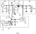
- Fig. 3 shows a system where power from a power source 200 is converter by a DC-DC converter 300 and provided to a power consuming load 400 according to an embodiment.
- the power consuming load 400 is any, or any combination of: a camera, an audio equipment, a power over Ethernet (PoE) powered device.
- the DC-DC converter 300 comprises a primary side 310 and a secondary side 350.
- the primary side 310 and the secondary side 350 are bridged by a transformer 340.
- the primary side 310 comprises a switch 320.
- the secondary side 350 is electrically couplable to the power consuming load 400.
- the DC-DC converter 300 further comprises a snubber circuit 500.
- the snubber circuit 500 is arranged to connect the primary side 310 with the secondary side 350.
- the snubber circuit 500 is connected between the drain terminal of the MOSFET transistor (representing the switch 320) at the primary side 310 and after the diode DR1 at the secondary side 350.
- the switch 320 is a MOSFET transistor having a gate terminal, a drain terminal, and a source terminal.
- the snubber circuit 500 is then connected at the drain terminal of the MOSFET transistor.
- the switch 320 might instead be an IGBT transistor having a gate terminal, a collector terminal, and an emitter terminal.
- the snubber circuit 500 is then connected at the collector terminal of the IGBT transistor.
- the snubber circuit 500 at the primary side 310 is connected at same voltage potential as the switch 320.
- the snubber circuit 500 comprises a capacitor 530, a rectifier 510 and an impedance balancing unit 520.
- the rectifier 510 might be a diode or an actively controlled switching element.
- the snubber circuit 500 thus adds an additional feed-forward path from the primary side to the secondary side of the transformer.
- an additional current ir2 is added to the load, increasing the output power, whereby power/energy from ringings, or oscillations, related to parasitic inductance and capacitance are also included in the current ir2.
- the snubber circuit 500 is arranged to convert oscillations resulting from opening of the switch 320 to a current for driving the power consuming load 400. This increases reliability, output power, and power-efficiency of the DC-DC converter in a cost-effective way, without the need of special components (which could be expensive).
- the herein disclosed arrangement of the snubber circuit in the DC-DC converter can hence be used to enhance the power efficiency of a traditional isolated DC-DC converter in a fly-back configuration, by converting unwanted parasitic ringings, or oscillations, due to component parasitics, to wanted load current. This improves reliability, whilst reducing the power losses associated with Resistor-Capacitor (RC) or Resistor-Capacitor-Diode (RCD) snubber circuits and at the same time increasing the output power of the DC-DC converter.
- RC Resistor-Capacitor
- RCD Resistor-Capacitor-Diode
- the arrangement of the snubber circuit in the DC-DC converter is used to mitigate ringings, or oscillations, by feeding the energy to the output load (as represented by the capacitor CL and the resistor RL).
- the snubber circuit can be used to supply charge, or energy, to the output of the DC-DC converter when the switch 320 is in the off-state. That is, the switch 320 is switchable between an on-state and an off-state. In the on-state a current is enabled to flow through the primary side 310 for the primary side 310 to transfer electrical energy to the secondary side 350. In the off-state the current is prevented from flowing through the primary side 310.
- the snubber circuit 500 provides current to the power consuming load 400 at the secondary side 350.
- the current will not flow through the primary side, but the current will still flow through the primary inductance (LP) to the parasitic output capacitance CPar of the switch.
- a controller 330 is arranged to periodically switch the switch 320 between the on-state and the off-state.
- a feedback path might be provided from the secondary side 350 to the controller 330.
- the feedback path might be realized as an optical connection, in contrast to an electrical connection, between the secondary side 350 and the controller 330.
- That the snubber circuit can be used to supply charge, or energy, to the output of the DC-DC converter when the switch 320 is in the off-state means that the maximum output power of the DC-DC converter can be doubled, mainly because the same amount of power is delivered throughout the whole waveform period (instead of during a half-period of the signal provided by the controller 330).
- Fig. 4 illustrates a DC-DC converter 300 in terms of a fly-back converter according to an embodiment.
- the snubber circuit 500 comprises an impedance balancing unit 520 (denoted ZFF), connected between a high-voltage capacitor CFF and a secondary rectifier DR2. An additional isolation barrier from the primary side 310 to the secondary side 350 of the DC-DC converter 300 is generated by the capacitor CFF. Together with the impedance balancing unit 520, a voltage-divider with impedance transformation is created. This type of circuit can be used to transform a low impedance in to a high one, exactly like the transformer).
- characteristics of the capacitor 530, the rectifier 510, and the impedance balancing unit 520 are adaptively settable as a function of required power of the power consuming load 400.
- Fig. 5 shows the same circuit as in Fig. 4 but where the DC-DC converter 300 is a fly-forward converter and where an additional inductance (LL) has been added in series with the diode DR1.
- LL additional inductance
- the impedance balancing unit 520 comprises an impedance transformation network, or an impedance matching network.
- the impedance balancing unit 520 is composed of at least one of: a resistor, an inductor, a capacitor, a transformer.
- the resistor, the inductor and the capacitor form a resistor-inductor-capacitor (RLC) circuit.
- the impedance balancing unit might comprise one inductor or multiple inductors, one capacitor or multiple capacitors, or one inductor together with one capacitor, or multiple inductors together with multiple capacitors, etc.
- resistance is a part of all real components, but can also be used to balance the loading of Vdrain or to generate high impedance paths to signal ground, for instance.
- the impedance balancing unit 520 might in some examples comprise of inductors and capacitors, connected as either a L-,T-, or ⁇ -network or a combination thereof.
- Figs. 6 to Fig. 11 Some examples of implementations of the impedance balancing unit can be found in Figs. 6 to Fig. 11 .
- Fig. 6 is illustrated three examples of impedance balancing units realized as a shunt capacitor 601 ( Fig. 6(a) ), a shunt inductor 602 ( Fig. 6(b) ), and a series inductor 603 ( Fig. 6(c) ).
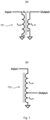
- Fig. 7 is illustrated two examples of transformer impedance balancing units realized as an isolated transformer 701 ( Fig. 7(a) ), and a non-isolated autotransformer 702 ( Fig. 7(b) ).
- Fig. 6 is illustrated three examples of impedance balancing units realized as a shunt capacitor 601 ( Fig. 6(a) ), a shunt inductor 602 ( Fig. 6(b) ), and a series inductor 603 ( Fig. 6(c) ).
- LC-filter based impedance balancing units realized as a low-pass impedance balancing unit 801 ( Fig. 8(a) ), and a high-pass impedance balancing unit 802 ( Fig. 8(b) ).
- the filters are used to transform the low impedance of the power consuming load 400 to a higher impedance.
- Fig. 8(a) low-pass impedance balancing unit 801
- Fig. 8(b) high-pass impedance balancing unit 802
- a harmonic resonance-based impedance balancing unit 901 with impedance matching values of LSh3,FF and CSh3,FF are selected to resonate at the third harmonic (giving a low impedance Z ⁇ o ⁇ ), whereas values of LSh5,FF and CSh5,FF are selected to resonate at the fifth harmonic (giving a low impedance Z ⁇ o ⁇ ).
- the multiple resonators can be used to shape voltage-and current-waveforms, and this shaping can be used to reduce the voltage and current overlap at the drain of the switch.
- Fig. 10 is illustrated an example of a T-match impedance balancing unit 1001 with a shunt diode rectifier.
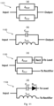
- Fig. 11 are illustrated four examples of multipath impedance balancing units, where Z FF,HF is for mitigating ringings, or oscillations, and Z FF,LF is for adjusting power.
- Fig. 11(a) is shown a general block diagram 1101
- Fig. 11(b) shows a realization 1102 of the block diagram in Fig. 11(a) with one capacitor and one inductor in parallel
- Fig. 11(c) shows a block diagram 1103 of a split path system
- Fig. 11(d) shows a realization 1104 of the block diagram in Fig. 11(c) with one capacitor and a diode in series, and one inductor.
- the impedance balancing unit and rectifiers are split into a high frequency part (such as to operate in the range of 10-50MHz) for the ringings, or oscillations, and a low frequency part (such as to operate in the range of 100kHz-10MHz, matching the operating frequency of the switch) to boost the output power of the converter, whilst feeding the current to the power consuming load 400.
- the rectifiers (one for Z FF,HF and one for Z FF,LF ) can also be optimized for operation at different power requirements and with different tolerances.
- the switch/rectifier of the low frequency network can be controlled to only deliver current when the DC-DC converter 300 cannot deliver more current. This requires more control of the rectifier of the low frequency circuitry, therefore an increase in overall circuit complexity, due to the large degrees of freedom.
- Additional functionality can be implemented in the impedance balancing unit 520 and/or the secondary rectifier DR2.
- One non-limiting example of such functionality is to implement an output power threshold, which enables, or increases, the power transfer from the snubber circuit 500 when the delivery of more power to the load 400 is needed. This gives a larger power range with good efficiency of the DC-DC converter and also increases the output power.
- ZVS Zero Voltage Switching
- the snubber circuit 500 comprises a further capacitor CSh,FF placed in parallel with the switch 320.
- the tuning of Z FF and C FF sets the amount of loading at V drain and the controlling of the rectifier sets when the loading of V drain occurs.
- Fig. 12(a) shows an example of a fly-back DC-DC converter with a snubber circuit arranged for ZVS. Examples of voltage- and current-waveforms of this fly-back DC-DC converter are shown in Fig. 12(b) and Fig. 12(c) .
- Fig. 13 is illustrated six different examples of the rectifier 510.
- Fig. 13(a) shows a rectifier 1301 realized by a diode in series and a shunt switch.
- Fig. 13(b) shows a rectifier 1302 realized by a switch in series together with a shunt switch.
- Fig. 13(c) shows a general series MOSFET switch rectifier 1303 (which could be realized either using a NMOS transistor or a PMOS transistor).
- Fig. 13(d) shows an active rectifier 1304 with a MOSFET switch and a gate driver controller.
- the voltage Vs supplies the gate driver with supply voltage and senses when to turn on the transistor MR in relation to the voltage terminal Vd (connected to the power consuming load 400), where Vg is the terminal that drives the gate of the transistor MR.
- Fig. 13(e) shows a shunt diode rectifier 1305.
- Fig. 13(f) shows a series diode rectifier with a shunt diode rectifier 1306.
Landscapes
- Engineering & Computer Science (AREA)
- Power Engineering (AREA)
- Dc-Dc Converters (AREA)
Abstract
There is provided a DC-DC converter (300). The DC-DC converter (300) comprises a primary side (310) and a secondary side (350). The primary side (310) and the secondary side (350) are bridged by a transformer (340), the primary side (310) comprises a switch (320). The DC-DC converter (300) further comprises a snubber circuit (500). The snubber circuit (500) is arranged to connect the primary side (310) with the secondary side (350). The snubber circuit (500) at the primary side (310) is connected at same voltage potential as the switch (320). The snubber circuit (500) comprises a capacitor (530), a rectifier (510) and an impedance balancing unit (520).
Description
- Embodiments presented herein relate to a DC-to-DC converter comprising a snubber circuit.
- In general terms, a DC-to-DC converter, or simply DC-DC converter, is an electronic circuit, or electromechanical device, that converts a source of direct current (DC) from one voltage level to another.
Fig. 1 schematically illustrates asystem 100 where power from apower source 200 is converter by a DC-DC converter 300 and provided to aload 400. - Operation of the
system 100 will be briefly explained next with reference toFig. 2. Fig. 2 illustrates simplified schematics of a DC-DC converter 300 realized as an isolated fly-back DC-DC converter, together with simplified schematics of thepower source 200 and theload 400. Thepower source 200 is modelled by a voltage source, providing +48 V, and a capacitor CIN. Theload 400 is represented by a decoupling capacitor CL and an output load resistor RL. The main body of the DC-DC converter 300 is composed of anisolation transformer 340 with an inductor LP at the primary side and an inductor LS at the secondary side) a MOSFET transistor MS defining aswitch 320, a rectifier (provided as the diode DRi), and acontroller 330. LPar represents the parasitic inductance of the transformer. CPar represents the parasitic output capacitance of theswitch 320. - The inductor LP at the primary side of the transformer is connected to the input DC supply voltage VIN and to the
switch 320. Thecontroller 330 is arranged to controllably cause theswitch 320 to switch between an on-state and an off-state. In this respect, the gate terminal Vgate of the MOSFET transistor might be driven by a Pulse-Width-Modulated (PWM) signal, a Pulse Frequency Modulation (PFM) signal, a Pulse Density/Duration Modulation (PDM) signal, or other type of control signal, fed from thecontroller 330, as illustrated by the pulse train inFig. 2 . This control signal is used to set the output DC voltage VOUT to the correct voltage, by the use of negative feedback. Further, thecontroller 330 might comprise, or be coupled to, current sensing, as represented by the current Is, of the source current of theswitch 320. In some alternatives, anexplicit controller 330 is not needed, such as when theswitch 320 is a self-oscillating switch, where gate-biasing is used for the control, where an inductor is connected between the Vgate and a gate-bias voltage. By using theswitch 320, the voltage VP over inductor LP at the primary side is approximately equal to VIN when the switch is in the on-state and this results in a current flowing from VIN through the inductor LP and through the MOSFET transformer (from its drain terminal to its source terminal). An inverted and scaled up (by a factor N:1) version of the current at the primary side is then present at the secondary side of the transformer, i.e., through the inductor LS. The current through the inductor LS at the secondar side increases the voltage VS above the output DC voltage (VOUT) and when the voltage is larger than the turn-on (anywhere from 0.1-0.7V) voltage of the rectifier DR1, a current in flows through the rectifier to the decoupling capacitor CL, which stores the energy/voltage in the form of charges. This means that the voltage VS, during rectifier conductance is VS = VOUT + Vn. As the right amount of current, charge, or energy is supplied to the decoupling capacitor CL, theswitch 320 is turned off (as controlled by the controller 330). - Because the transformer is inductive, at the moment when the
switch 320 is turned off, the primary voltage VP can swing above VIN (due to the fact that an inductor is a short-circuit for DC signals). The transformer primary voltage (with the switched 320 in the off-state) can be calculated as VP = VIN + N·VS and Vdrain = VP, when ideal components are assumed. For components with parasitics, mainly leakage inductance in the transformer (LPar) and parasitic capacitance in the switch 320 (such as mainly drain to GND capacitances during the off state), might generate additional voltage ringings, or oscillations, across theswitch 320; Vdrain ≥ 2·VIN+N·VS. These ringings, or oscillations, might cause reliability issues. In a worst-case situation, even breakdown of theswitch 320 might be caused due to oxide-breakdown, resulting from the voltage ringings, or oscillations. - Hence, there is still a need for an improved DC-DC converter.
- An object of embodiments herein is to provide a DC-DC converter that does not suffer from the above issues.
- According to one aspect there is presented a DC-DC converter. The DC-DC converter comprises a primary side and a secondary side. The primary side and the secondary side are bridged by a transformer. The primary side comprises a switch. The DC-DC converter further comprises a snubber circuit. The snubber circuit is arranged to connect the primary side with the secondary side. The snubber circuit at the primary side is connected at the same voltage potential as the switch. The snubber circuit comprises a capacitor, a rectifier and an impedance balancing unit.
- Advantageously, the snubber circuit can be used with existing DC-DC converters to boost the performance but without requiring any additional design changes to the DC-DC converters.
- Advantageously, the disclosed DC-DC converter provides increased reliability, output power, and efficiency, without increasing the cost per unit of power. As an example, with the disclosed configuration, a DC-DC converter for POE class 3 can, by provision of the snubber circuit, be upgraded to
POE class 4 without any further change of components. - Advantageously, the disclosed DC-DC converter increases the output power without the need for more expensive components whilst reducing the stress of the components, due to heat and voltage overshoots.
- Advantageously, due to the fact that current, or charge, is delivered to the output of the DC-DC converter during each half-period, less output capacitance is required (thus lowering cost) and also no freewheel half-period for driving the load is present. In turn, this means that no energy, or power, is burnt off without delivering power to the load.
- Advantageously, the resistance used to attenuate the parasitic ringings, or oscillations, is the output load of the DC-DC converter and this also means that the snubber circuit can be adapted to the required output power.
- Other objectives, features and advantages of the enclosed embodiments will be apparent from the following detailed disclosure, from the attached dependent claims as well as from the drawings.
- Generally, all terms used in the claims are to be interpreted according to their ordinary meaning in the technical field, unless explicitly defined otherwise herein. All references to "a/an/the element, apparatus, component, means, module, step, etc." are to be interpreted openly as referring to at least one instance of the element, apparatus, component, means, module, step, etc., unless explicitly stated otherwise. The steps of any method disclosed herein do not have to be performed in the exact order disclosed, unless explicitly stated.
- The inventive concept is now described, by way of example, with reference to the accompanying drawings, in which:
-
Fig. 1 schematically illustrates a system where power from a power source is converter by a DC-DC converter and provided to a load according to an example; -
Fig. 2 provides schematics of a DC-DC converter, a power source, and a load according to an example; -
Figs. 3 ,4 , and5 provides schematics of a DC-DC converter, a power source, and a load according to embodiments; -
Figs. 6 ,7 ,8 ,9 ,10 , and11 schematically illustrate examples of impedance balancing units according to embodiments; -
Fig. 12 schematically illustrates a DC-DC converter and voltage- and current-waveforms according to an embodiment; and -
Fig. 13 schematically illustrates examples of a rectifier according to embodiments. - The inventive concept will now be described more fully hereinafter with reference to the accompanying drawings, in which certain embodiments of the inventive concept are shown. This inventive concept may, however, be embodied in many different forms and should not be construed as limited to the embodiments set forth herein; rather, these embodiments are provided by way of example so that this disclosure will be thorough and complete, and will fully convey the scope of the inventive concept to those skilled in the art. Like numbers refer to like elements throughout the description. Any feature illustrated by dashed lines should be regarded as optional.
- Reference is next made to
Fig. 3 which shows a system where power from apower source 200 is converter by a DC-DC converter 300 and provided to apower consuming load 400 according to an embodiment. In some non-limiting examples, thepower consuming load 400 is any, or any combination of: a camera, an audio equipment, a power over Ethernet (PoE) powered device. Some of the components are the same as in the system inFig. 2 . Hence, the DC-DC converter 300 comprises aprimary side 310 and asecondary side 350. Theprimary side 310 and thesecondary side 350 are bridged by atransformer 340. Theprimary side 310 comprises aswitch 320. Thesecondary side 350 is electrically couplable to thepower consuming load 400. The DC-DC converter 300 further comprises asnubber circuit 500. Thesnubber circuit 500 is arranged to connect theprimary side 310 with thesecondary side 350. According toFig. 3 , thesnubber circuit 500 is connected between the drain terminal of the MOSFET transistor (representing the switch 320) at theprimary side 310 and after the diode DR1 at thesecondary side 350. That is, in some examples, theswitch 320 is a MOSFET transistor having a gate terminal, a drain terminal, and a source terminal. Thesnubber circuit 500 is then connected at the drain terminal of the MOSFET transistor. Further, theswitch 320 might instead be an IGBT transistor having a gate terminal, a collector terminal, and an emitter terminal. Thesnubber circuit 500 is then connected at the collector terminal of the IGBT transistor. Thesnubber circuit 500 at theprimary side 310 is connected at same voltage potential as theswitch 320. As will be disclosed in more detail below with reference toFig. 4 , thesnubber circuit 500 comprises acapacitor 530, arectifier 510 and animpedance balancing unit 520. Therectifier 510 might be a diode or an actively controlled switching element. - The
snubber circuit 500 thus adds an additional feed-forward path from the primary side to the secondary side of the transformer. By adding such an additional feed-forward path, an additional current ir2 is added to the load, increasing the output power, whereby power/energy from ringings, or oscillations, related to parasitic inductance and capacitance are also included in the current ir2. In particular, in some embodiments, thesnubber circuit 500 is arranged to convert oscillations resulting from opening of theswitch 320 to a current for driving thepower consuming load 400. This increases reliability, output power, and power-efficiency of the DC-DC converter in a cost-effective way, without the need of special components (which could be expensive). - The herein disclosed arrangement of the snubber circuit in the DC-DC converter can hence be used to enhance the power efficiency of a traditional isolated DC-DC converter in a fly-back configuration, by converting unwanted parasitic ringings, or oscillations, due to component parasitics, to wanted load current. This improves reliability, whilst reducing the power losses associated with Resistor-Capacitor (RC) or Resistor-Capacitor-Diode (RCD) snubber circuits and at the same time increasing the output power of the DC-DC converter.
- The arrangement of the snubber circuit in the DC-DC converter is used to mitigate ringings, or oscillations, by feeding the energy to the output load (as represented by the capacitor CL and the resistor RL). In addition, the snubber circuit can be used to supply charge, or energy, to the output of the DC-DC converter when the
switch 320 is in the off-state. That is, theswitch 320 is switchable between an on-state and an off-state. In the on-state a current is enabled to flow through theprimary side 310 for theprimary side 310 to transfer electrical energy to thesecondary side 350. In the off-state the current is prevented from flowing through theprimary side 310. In the off-state thesnubber circuit 500 provides current to thepower consuming load 400 at thesecondary side 350. In further detail, in the off-state the current will not flow through the primary side, but the current will still flow through the primary inductance (LP) to the parasitic output capacitance CPar of the switch. - A
controller 330 is arranged to periodically switch theswitch 320 between the on-state and the off-state. A feedback path might be provided from thesecondary side 350 to thecontroller 330. The feedback path might be realized as an optical connection, in contrast to an electrical connection, between thesecondary side 350 and thecontroller 330. - That the snubber circuit can be used to supply charge, or energy, to the output of the DC-DC converter when the
switch 320 is in the off-state means that the maximum output power of the DC-DC converter can be doubled, mainly because the same amount of power is delivered throughout the whole waveform period (instead of during a half-period of the signal provided by the controller 330). - With reference next being made to
Fig. 4 , which illustrates a DC-DC converter 300 in terms of a fly-back converter according to an embodiment. Thesnubber circuit 500 comprises an impedance balancing unit 520 (denoted ZFF), connected between a high-voltage capacitor CFF and a secondary rectifier DR2. An additional isolation barrier from theprimary side 310 to thesecondary side 350 of the DC-DC converter 300 is generated by the capacitor CFF. Together with theimpedance balancing unit 520, a voltage-divider with impedance transformation is created. This type of circuit can be used to transform a low impedance in to a high one, exactly like the transformer). In some embodiments, characteristics of thecapacitor 530, therectifier 510, and theimpedance balancing unit 520 are adaptively settable as a function of required power of thepower consuming load 400.Fig. 5 shows the same circuit as inFig. 4 but where the DC-DC converter 300 is a fly-forward converter and where an additional inductance (LL) has been added in series with the diode DR1. - In some examples, the
impedance balancing unit 520 comprises an impedance transformation network, or an impedance matching network. In some examples, theimpedance balancing unit 520 is composed of at least one of: a resistor, an inductor, a capacitor, a transformer. In some examples the resistor, the inductor and the capacitor form a resistor-inductor-capacitor (RLC) circuit. Still further, the impedance balancing unit might comprise one inductor or multiple inductors, one capacitor or multiple capacitors, or one inductor together with one capacitor, or multiple inductors together with multiple capacitors, etc. For the resistor part, resistance is a part of all real components, but can also be used to balance the loading of Vdrain or to generate high impedance paths to signal ground, for instance. Theimpedance balancing unit 520 might in some examples comprise of inductors and capacitors, connected as either a L-,T-, or π-network or a combination thereof. - Some examples of implementations of the impedance balancing unit can be found in
Figs. 6 to Fig. 11 . InFig. 6 is illustrated three examples of impedance balancing units realized as a shunt capacitor 601 (Fig. 6(a) ), a shunt inductor 602 (Fig. 6(b) ), and a series inductor 603 (Fig. 6(c) ). InFig. 7 is illustrated two examples of transformer impedance balancing units realized as an isolated transformer 701 (Fig. 7(a) ), and a non-isolated autotransformer 702 (Fig. 7(b) ). InFig. 8 is illustrated two examples of LC-filter based impedance balancing units realized as a low-pass impedance balancing unit 801 (Fig. 8(a) ), and a high-pass impedance balancing unit 802 (Fig. 8(b) ). The filters are used to transform the low impedance of thepower consuming load 400 to a higher impedance. InFig. 9 is illustrated an example of a harmonic resonance-basedimpedance balancing unit 901 with impedance matching; values of LSh3,FF and CSh3,FF are selected to resonate at the third harmonic (giving a low impedance Z≈oΩ), whereas values of LSh5,FF and CSh5,FF are selected to resonate at the fifth harmonic (giving a low impedance Z≈oΩ). This tunes the current into a square-wave, which gives less voltage to current overlap in the switch. The multiple resonators can be used to shape voltage-and current-waveforms, and this shaping can be used to reduce the voltage and current overlap at the drain of the switch. InFig. 10 is illustrated an example of a T-matchimpedance balancing unit 1001 with a shunt diode rectifier. InFig. 11 are illustrated four examples of multipath impedance balancing units, where ZFF,HF is for mitigating ringings, or oscillations, and ZFF,LF is for adjusting power. InFig. 11(a) is shown a general block diagram 1101,Fig. 11(b) shows arealization 1102 of the block diagram inFig. 11(a) with one capacitor and one inductor in parallel,Fig. 11(c) shows a block diagram 1103 of a split path system, andFig. 11(d) shows arealization 1104 of the block diagram inFig. 11(c) with one capacitor and a diode in series, and one inductor. According toFig. 11(c) and Fig. 11(d) , the impedance balancing unit and rectifiers are split into a high frequency part (such as to operate in the range of 10-50MHz) for the ringings, or oscillations, and a low frequency part (such as to operate in the range of 100kHz-10MHz, matching the operating frequency of the switch) to boost the output power of the converter, whilst feeding the current to thepower consuming load 400. The rectifiers (one for ZFF,HF and one for ZFF,LF) can also be optimized for operation at different power requirements and with different tolerances. The switch/rectifier of the low frequency network can be controlled to only deliver current when the DC-DC converter 300 cannot deliver more current. This requires more control of the rectifier of the low frequency circuitry, therefore an increase in overall circuit complexity, due to the large degrees of freedom. - Additional functionality can be implemented in the
impedance balancing unit 520 and/or the secondary rectifier DR2. One non-limiting example of such functionality is to implement an output power threshold, which enables, or increases, the power transfer from thesnubber circuit 500 when the delivery of more power to theload 400 is needed. This gives a larger power range with good efficiency of the DC-DC converter and also increases the output power. - Aspects of Zero Voltage Switching (ZVS) will be disclosed next with reference to the
circuit scheme 1201 inFig. 12 . ZVS can be achieved by tuning the impedance balancing unit together with CFF and to control the ZVS by controlling when the rectifier is turned on. Thesnubber circuit 500 comprises a further capacitor CSh,FF placed in parallel with theswitch 320. The tuning of ZFF and CFF sets the amount of loading at Vdrain and the controlling of the rectifier sets when the loading of Vdrain occurs.Fig. 12(a) shows an example of a fly-back DC-DC converter with a snubber circuit arranged for ZVS. Examples of voltage- and current-waveforms of this fly-back DC-DC converter are shown inFig. 12(b) and Fig. 12(c) . - In
Fig. 13 is illustrated six different examples of therectifier 510.Fig. 13(a) shows arectifier 1301 realized by a diode in series and a shunt switch.Fig. 13(b) shows arectifier 1302 realized by a switch in series together with a shunt switch.Fig. 13(c) shows a general series MOSFET switch rectifier 1303 (which could be realized either using a NMOS transistor or a PMOS transistor).Fig. 13(d) shows anactive rectifier 1304 with a MOSFET switch and a gate driver controller. The voltage Vs supplies the gate driver with supply voltage and senses when to turn on the transistor MR in relation to the voltage terminal Vd (connected to the power consuming load 400), where Vg is the terminal that drives the gate of the transistor MR.Fig. 13(e) shows ashunt diode rectifier 1305. Finally,Fig. 13(f) shows a series diode rectifier with ashunt diode rectifier 1306. - The inventive concept has mainly been described above with reference to a few embodiments. However, as is readily appreciated by a person skilled in the art, other embodiments than the ones disclosed above are equally possible within the scope of the inventive concept, as defined by the appended patent claims.
Claims (13)
- A direct current to direct current, DC-DC, converter (300), the DC-DC converter (300) comprising:a primary side (310) and a secondary side (350), the primary side (310) and the secondary side (350) being bridged by a transformer (340), the primary side (310) comprising a switch (320); anda snubber circuit (500),wherein the snubber circuit (500) is arranged to connect the primary side (310) with the secondary side (350),wherein the snubber circuit (500) at the primary side (310) is connected at same voltage potential as the switch (320), andwherein the snubber circuit (500) comprises a capacitor (530), a rectifier (510) and an impedance balancing unit (520).
- The DC-DC converter (300) according to claim 1, wherein the impedance balancing unit (520) comprises an impedance transformation, or impedance matching, network.
- The DC-DC converter (300) according to claim 2, wherein the impedance balancing unit (520) is composed of at least one of: a resistor, an inductor, a capacitor, a transformer.
- The DC-DC converter (300) according to any preceding claim, wherein the secondary side (350) is electrically couplable to a power consuming load (400), and wherein the snubber circuit (500) is arranged to convert oscillations resulting from opening of the switch (320) to a current for driving the power consuming load (400).
- The DC-DC converter (300) according to claim 4, wherein characteristics of the capacitor (530), the rectifier (510), and the impedance balancing unit (520) are adaptively settable as a function of required power of the power consuming load (400).
- The DC-DC converter (300) according to claim 4 or 5, wherein the power consuming load (400) is any, or any combination of: a camera, an audio equipment, a power over Ethernet powered device.
- The DC-DC converter (300) according to claim 4, 5 or 6, wherein the switch (320) is switchable between an on-state and an off-state, wherein in the on-state a current is enabled to flow through the primary side (310) for the primary side (310) to transfer electrical energy to the secondary side (350) and in the off-state the current is prevented from flowing through the primary side (310), and wherein in the off-state the snubber circuit (500) provides current to the power consuming load (400) at the secondary side (350).
- The DC-DC converter (300) according to claim 7, further comprising:
a controller (330) arranged to periodically switch the switch (320) between the on-state and the off-state. - The DC-DC converter (300) according to claim 8, further comprising a feedback path from the secondary side (350) to the controller (330).
- The DC-DC converter (300) according to any preceding claim, wherein the snubber circuit (500) comprises a further capacitor (CSh,FF) placed in parallel with the switch (320).
- The DC-DC converter (300) according to any preceding claim, wherein the rectifier (510) is a diode or an actively controlled switching element.
- The DC-DC converter (300) according to any preceding claim, wherein the switch (320) is a MOSFET transistor having a gate terminal, a drain terminal, and a source terminal, and wherein the snubber circuit (500) is connected at the drain terminal of the MOSFET transistor, or wherein the switch (320) is an IGBT transistor having a gate terminal, a collector terminal, and an emitter terminal, and wherein the snubber circuit (500) is connected at the collector terminal of the IGBT transistor.
- The DC-DC converter (300) according to any preceding claim, wherein the DC-DC converter (300) is any of: a fly-back converter, a fly-forward converter.
Priority Applications (1)
| Application Number | Priority Date | Filing Date | Title |
|---|---|---|---|
| EP22197017.1A EP4344042A1 (en) | 2022-09-22 | 2022-09-22 | Dc-to-dc converter with snubber circuit |
Applications Claiming Priority (1)
| Application Number | Priority Date | Filing Date | Title |
|---|---|---|---|
| EP22197017.1A EP4344042A1 (en) | 2022-09-22 | 2022-09-22 | Dc-to-dc converter with snubber circuit |
Publications (1)
| Publication Number | Publication Date |
|---|---|
| EP4344042A1 true EP4344042A1 (en) | 2024-03-27 |
Family
ID=83438419
Family Applications (1)
| Application Number | Title | Priority Date | Filing Date |
|---|---|---|---|
| EP22197017.1A Pending EP4344042A1 (en) | 2022-09-22 | 2022-09-22 | Dc-to-dc converter with snubber circuit |
Country Status (1)
| Country | Link |
|---|---|
| EP (1) | EP4344042A1 (en) |
Citations (6)
| Publication number | Priority date | Publication date | Assignee | Title |
|---|---|---|---|---|
| US6005782A (en) * | 1998-10-16 | 1999-12-21 | Nortel Networks Corporation | Flyback converter with soft switching using auxiliary switch and resonant circuit |
| US6069803A (en) * | 1999-02-12 | 2000-05-30 | Astec International Limited | Offset resonance zero volt switching flyback converter |
| US20120182769A1 (en) * | 2011-01-13 | 2012-07-19 | Fujitsu Limited | Dc-dc converter, power supply unit and an information processing apparatus |
| US20130322129A1 (en) * | 2011-02-14 | 2013-12-05 | Fujitsu Limited | Power factor correction circuit |
| US20150326105A1 (en) * | 2014-05-06 | 2015-11-12 | National Tsing Hua University | Pulsating Current Ripple Cancelling Circuit and Power Converting System Using the Same |
| US20190296649A1 (en) * | 2018-03-26 | 2019-09-26 | L3 Cincinnati Electronics Corporation | Energy-Harvesting Power Supplies |
-
2022
- 2022-09-22 EP EP22197017.1A patent/EP4344042A1/en active Pending
Patent Citations (6)
| Publication number | Priority date | Publication date | Assignee | Title |
|---|---|---|---|---|
| US6005782A (en) * | 1998-10-16 | 1999-12-21 | Nortel Networks Corporation | Flyback converter with soft switching using auxiliary switch and resonant circuit |
| US6069803A (en) * | 1999-02-12 | 2000-05-30 | Astec International Limited | Offset resonance zero volt switching flyback converter |
| US20120182769A1 (en) * | 2011-01-13 | 2012-07-19 | Fujitsu Limited | Dc-dc converter, power supply unit and an information processing apparatus |
| US20130322129A1 (en) * | 2011-02-14 | 2013-12-05 | Fujitsu Limited | Power factor correction circuit |
| US20150326105A1 (en) * | 2014-05-06 | 2015-11-12 | National Tsing Hua University | Pulsating Current Ripple Cancelling Circuit and Power Converting System Using the Same |
| US20190296649A1 (en) * | 2018-03-26 | 2019-09-26 | L3 Cincinnati Electronics Corporation | Energy-Harvesting Power Supplies |
Similar Documents
| Publication | Publication Date | Title |
|---|---|---|
| US7345894B2 (en) | Cascode switch power supply | |
| CN203691238U (en) | Electronic converter and related illuminating system | |
| US9991805B2 (en) | On and off controlled resonant DC-DC power converter | |
| US7746670B2 (en) | Dual-transformer type of DC-to-DC converter | |
| US11437924B2 (en) | Switching power supply circuit | |
| KR102650677B1 (en) | Power converter with active clamp | |
| US11223271B2 (en) | Gate drive adapter | |
| US6188588B1 (en) | Switching controller and method for operating a flyback converter in a critically continuous conduction mode | |
| JP2000134920A (en) | Drive compensating circuit for synchronous rectifier and method for actuating the same | |
| CA2889509A1 (en) | Self-oscillating resonant power converter | |
| US20100328971A1 (en) | Boundary mode coupled inductor boost power converter | |
| WO2009126728A2 (en) | Active snubber for transition mode power converter | |
| KR20010110659A (en) | General self-driven synchronous rectification scheme for synchronous rectifiers having a floating gate | |
| KR100681689B1 (en) | Switching power supply | |
| TW200417118A (en) | Control IC for low power auxiliary supplies | |
| JP2024154500A (en) | Power source device | |
| CN116131624A (en) | Power supply circuit, power supply system and electronic device | |
| EP2638628B1 (en) | Voltage converter comprising a storage inductor with one winding and a storage inductor with two windings | |
| JP2003134817A (en) | Power supply | |
| Eitzen et al. | Bidirectional power electronics for driving dielectric elastomer transducers | |
| US6442052B1 (en) | High efficiency power converter with fast transient response | |
| EP3656046A1 (en) | A dc-dc power converter with improved output current resolution | |
| US20240313656A1 (en) | Bias generation for power converter | |
| KR101456654B1 (en) | A common-core power factor correction resonant converter | |
| KR20070121827A (en) | A method of operating a switched mode power supply having a return of primary stray energy |
Legal Events
| Date | Code | Title | Description |
|---|---|---|---|
| PUAI | Public reference made under article 153(3) epc to a published international application that has entered the european phase |
Free format text: ORIGINAL CODE: 0009012 |
|
| STAA | Information on the status of an ep patent application or granted ep patent |
Free format text: STATUS: REQUEST FOR EXAMINATION WAS MADE |
|
| 17P | Request for examination filed |
Effective date: 20230522 |
|
| AK | Designated contracting states |
Kind code of ref document: A1 Designated state(s): AL AT BE BG CH CY CZ DE DK EE ES FI FR GB GR HR HU IE IS IT LI LT LU LV MC MK MT NL NO PL PT RO RS SE SI SK SM TR |
|
| STAA | Information on the status of an ep patent application or granted ep patent |
Free format text: STATUS: EXAMINATION IS IN PROGRESS |
|
| 17Q | First examination report despatched |
Effective date: 20251023 |