EP4343855A1 - Semiconductor device - Google Patents
Semiconductor device Download PDFInfo
- Publication number
- EP4343855A1 EP4343855A1 EP23159217.1A EP23159217A EP4343855A1 EP 4343855 A1 EP4343855 A1 EP 4343855A1 EP 23159217 A EP23159217 A EP 23159217A EP 4343855 A1 EP4343855 A1 EP 4343855A1
- Authority
- EP
- European Patent Office
- Prior art keywords
- electrode
- insulating film
- semiconductor
- control
- semiconductor part
- Prior art date
- Legal status (The legal status is an assumption and is not a legal conclusion. Google has not performed a legal analysis and makes no representation as to the accuracy of the status listed.)
- Withdrawn
Links
Images







Classifications
-
- H—ELECTRICITY
- H10—SEMICONDUCTOR DEVICES; ELECTRIC SOLID-STATE DEVICES NOT OTHERWISE PROVIDED FOR
- H10D—INORGANIC ELECTRIC SEMICONDUCTOR DEVICES
- H10D12/00—Bipolar devices controlled by the field effect, e.g. insulated-gate bipolar transistors [IGBT]
- H10D12/411—Insulated-gate bipolar transistors [IGBT]
- H10D12/441—Vertical IGBTs
- H10D12/461—Vertical IGBTs having non-planar surfaces, e.g. having trenches, recesses or pillars in the surfaces of the emitter, base or collector regions
- H10D12/481—Vertical IGBTs having non-planar surfaces, e.g. having trenches, recesses or pillars in the surfaces of the emitter, base or collector regions having gate structures on slanted surfaces, on vertical surfaces, or in grooves, e.g. trench gate IGBTs
-
- H—ELECTRICITY
- H10—SEMICONDUCTOR DEVICES; ELECTRIC SOLID-STATE DEVICES NOT OTHERWISE PROVIDED FOR
- H10D—INORGANIC ELECTRIC SEMICONDUCTOR DEVICES
- H10D12/00—Bipolar devices controlled by the field effect, e.g. insulated-gate bipolar transistors [IGBT]
- H10D12/01—Manufacture or treatment
- H10D12/031—Manufacture or treatment of IGBTs
- H10D12/032—Manufacture or treatment of IGBTs of vertical IGBTs
- H10D12/038—Manufacture or treatment of IGBTs of vertical IGBTs having a recessed gate, e.g. trench-gate IGBTs
-
- H—ELECTRICITY
- H10—SEMICONDUCTOR DEVICES; ELECTRIC SOLID-STATE DEVICES NOT OTHERWISE PROVIDED FOR
- H10D—INORGANIC ELECTRIC SEMICONDUCTOR DEVICES
- H10D62/00—Semiconductor bodies, or regions thereof, of devices having potential barriers
- H10D62/10—Shapes, relative sizes or dispositions of the regions of the semiconductor bodies; Shapes of the semiconductor bodies
- H10D62/124—Shapes, relative sizes or dispositions of the regions of semiconductor bodies or of junctions between the regions
- H10D62/126—Top-view geometrical layouts of the regions or the junctions
- H10D62/127—Top-view geometrical layouts of the regions or the junctions of cellular field-effect devices, e.g. multicellular DMOS transistors or IGBTs
-
- H—ELECTRICITY
- H10—SEMICONDUCTOR DEVICES; ELECTRIC SOLID-STATE DEVICES NOT OTHERWISE PROVIDED FOR
- H10D—INORGANIC ELECTRIC SEMICONDUCTOR DEVICES
- H10D62/00—Semiconductor bodies, or regions thereof, of devices having potential barriers
- H10D62/10—Shapes, relative sizes or dispositions of the regions of the semiconductor bodies; Shapes of the semiconductor bodies
- H10D62/17—Semiconductor regions connected to electrodes not carrying current to be rectified, amplified or switched, e.g. channel regions
- H10D62/393—Body regions of DMOS transistors or IGBTs
-
- H—ELECTRICITY
- H10—SEMICONDUCTOR DEVICES; ELECTRIC SOLID-STATE DEVICES NOT OTHERWISE PROVIDED FOR
- H10D—INORGANIC ELECTRIC SEMICONDUCTOR DEVICES
- H10D64/00—Electrodes of devices having potential barriers
- H10D64/01—Manufacture or treatment
-
- H—ELECTRICITY
- H10—SEMICONDUCTOR DEVICES; ELECTRIC SOLID-STATE DEVICES NOT OTHERWISE PROVIDED FOR
- H10D—INORGANIC ELECTRIC SEMICONDUCTOR DEVICES
- H10D64/00—Electrodes of devices having potential barriers
- H10D64/111—Field plates
- H10D64/117—Recessed field plates, e.g. trench field plates or buried field plates
-
- H—ELECTRICITY
- H10—SEMICONDUCTOR DEVICES; ELECTRIC SOLID-STATE DEVICES NOT OTHERWISE PROVIDED FOR
- H10D—INORGANIC ELECTRIC SEMICONDUCTOR DEVICES
- H10D64/00—Electrodes of devices having potential barriers
- H10D64/20—Electrodes characterised by their shapes, relative sizes or dispositions
- H10D64/27—Electrodes not carrying the current to be rectified, amplified, oscillated or switched, e.g. gates
- H10D64/311—Gate electrodes for field-effect devices
- H10D64/411—Gate electrodes for field-effect devices for FETs
- H10D64/511—Gate electrodes for field-effect devices for FETs for IGFETs
- H10D64/512—Disposition of the gate electrodes, e.g. buried gates
- H10D64/513—Disposition of the gate electrodes, e.g. buried gates within recesses in the substrate, e.g. trench gates, groove gates or buried gates
-
- H—ELECTRICITY
- H10—SEMICONDUCTOR DEVICES; ELECTRIC SOLID-STATE DEVICES NOT OTHERWISE PROVIDED FOR
- H10D—INORGANIC ELECTRIC SEMICONDUCTOR DEVICES
- H10D64/00—Electrodes of devices having potential barriers
- H10D64/20—Electrodes characterised by their shapes, relative sizes or dispositions
- H10D64/27—Electrodes not carrying the current to be rectified, amplified, oscillated or switched, e.g. gates
- H10D64/311—Gate electrodes for field-effect devices
- H10D64/411—Gate electrodes for field-effect devices for FETs
- H10D64/511—Gate electrodes for field-effect devices for FETs for IGFETs
- H10D64/517—Gate electrodes for field-effect devices for FETs for IGFETs characterised by the conducting layers
- H10D64/518—Gate electrodes for field-effect devices for FETs for IGFETs characterised by the conducting layers characterised by their lengths or sectional shapes
-
- H—ELECTRICITY
- H10—SEMICONDUCTOR DEVICES; ELECTRIC SOLID-STATE DEVICES NOT OTHERWISE PROVIDED FOR
- H10D—INORGANIC ELECTRIC SEMICONDUCTOR DEVICES
- H10D64/00—Electrodes of devices having potential barriers
- H10D64/20—Electrodes characterised by their shapes, relative sizes or dispositions
- H10D64/27—Electrodes not carrying the current to be rectified, amplified, oscillated or switched, e.g. gates
- H10D64/311—Gate electrodes for field-effect devices
- H10D64/411—Gate electrodes for field-effect devices for FETs
- H10D64/511—Gate electrodes for field-effect devices for FETs for IGFETs
- H10D64/517—Gate electrodes for field-effect devices for FETs for IGFETs characterised by the conducting layers
- H10D64/519—Gate electrodes for field-effect devices for FETs for IGFETs characterised by the conducting layers characterised by their top-view geometrical layouts
Definitions
- Embodiments relate to a semiconductor device.
- a semiconductor device includes a semiconductor part, first to fourth electrodes and a control electrode.
- the first electrode is provided on a back surface of the semiconductor part; and the second electrode is provided on a front surface of the semiconductor part at a side opposite to the back surface.
- the third electrode is provided between the first electrode and the second electrode, and provided in the semiconductor part with a first insulating film interposed.
- the third electrode is electrically insulated from the semiconductor part by the first insulating film.
- the control electrode is provided between the second electrode and the third electrode. The control electrode extends into the semiconductor part from the front side of the semiconductor part and faces the third electrode with a second insulating film interposed.
- the first insulating film extends between the semiconductor part and the control electrode and electrically insulates the control electrode from the semiconductor part.
- the fourth electrode is provided between the second electrode and the third electrode. The fourth electrode extends into the semiconductor part from the front side of the semiconductor part and is positioned between the semiconductor part and the control electrode.
- the first insulating film extends between the semiconductor part and the fourth electrode; and the second insulating film extends between the third electrode and the fourth electrode.
- the fourth electrode faces the control electrode with a third insulating film interposed; and the fourth electrode is electrically connected to the third electrode.
- FIG. 1 is a schematic cross-sectional view showing a semiconductor device 1 according to an embodiment.
- the semiconductor device 1 is, for example, an IGBT (Insulated Gate Bipolar Transistor).
- the semiconductor device 1 includes a semiconductor part 10, a first electrode 20, a second electrode 30, a control electrode 40, a third electrode 50, and a fourth electrode 60.
- the semiconductor part 10 is, for example, silicon.
- the semiconductor part 10 is provided between the first electrode 20 and the second electrode 30.
- the first electrode 20 is, for example, a collector electrode and is provided on a back surface 10B of the semiconductor part 10.
- the second electrode 30 is, for example, an emitter electrode and is provided on a front surface 10F of the semiconductor part 10 at the side opposite to the back surface 10B.
- the control electrode 40, the third electrode 50, and the fourth electrode 60 are positioned, for example, between the first electrode 20 and the second electrode 30.
- the semiconductor part 10 includes, for example, a gate trench GT provided at the front surface 10F side.
- the control electrode 40, the third electrode 50, and the fourth electrode 60 are provided in the gate trench GT.
- the control electrode 40 is, for example, a gate electrode.
- the control electrode 40 extends into the semiconductor part 10 from the front surface 10F side of the semiconductor part 10.
- the control electrode 40 is electrically insulated from the semiconductor part 10 by a first insulating film 21.
- the first insulating film 21 is, for example, a gate insulating film.
- the third electrode 50 is provided inside the semiconductor part 10 and is electrically insulated from the semiconductor part 10 by, for example, the first insulating film 21.
- the first insulating film 21 extends between the semiconductor part 10 and the third electrode 50.
- the third electrode 50 is positioned between the first electrode 20 and the control electrode 40.
- the control electrode 40 is provided between the second electrode 30 and the third electrode 50.
- the control electrode 40 faces the third electrode 50 via a second insulating film 23.
- the control electrode 40 is electrically insulated from the third electrode 50 by the second insulating film 23.
- the fourth electrode 60 also extends into the semiconductor part 10 from the front surface 10F side of the semiconductor part 10.
- the fourth electrode 60 is provided between the second electrode 30 and the third electrode 50.
- the second insulating film 23 extends between the third electrode 50 and the fourth electrode 60; and the fourth electrode 60 faces the third electrode 50 via the second insulating film 23.
- the fourth electrode 60 is positioned between the semiconductor part 10 and the control electrode 40.
- the first insulating film 21 extends between the semiconductor part 10 and the fourth electrode 60 and electrically insulates the fourth electrode 60 from the semiconductor part 10.
- the fourth electrode 60 faces the control electrode 40 via a third insulating film 25.
- the fourth electrode 60 is electrically insulated from the control electrode 40 by the third insulating film 25.
- the fourth electrode 60 is electrically connected to the third electrode 50 (see FIG. 4B ).
- the control electrode 40 and the fourth electrode 60 are electrically insulated from the second electrode 30 by a fourth insulating film 27.
- the fourth insulating film 27 is, for example, an inter-layer insulating film.
- the third electrode 50 and the fourth electrode 60 serve as, for example, a second control electrode.
- the semiconductor part 10 includes a first semiconductor layer 11 of a first conductivity type, a second semiconductor layer 13 of a second conductivity type, a third semiconductor layer 15 of the first conductivity type, and a fourth semiconductor layer 17 of the second conductivity type.
- first conductivity type is described as an n-type and the second conductivity type is described as a p-type, but the embodiments are not limited thereto.
- the first semiconductor layer 11 is, for example, an n-type base layer.
- the first semiconductor layer 11 extends between the first electrode 20 and the second electrode 30.
- the third electrode 50 is positioned inside the first semiconductor layer 11 and faces the first semiconductor layer 11 via the first insulating film 21.
- the second semiconductor layer 13 is, for example, a p-type base layer.
- the second semiconductor layer 13 is provided between the first semiconductor layer 11 and the second electrode 30.
- the second semiconductor layer 13 faces the control electrode 40 via the first insulating film 21.
- the semiconductor part 10 further includes another second semiconductor layer 13; and the control electrode 40 and the fourth electrode 60 are positioned between the second semiconductor layer 13 and the other second semiconductor layer 13.
- the other second semiconductor layer 13 faces the fourth electrode 60 via the first insulating film 21.
- the third semiconductor layer 15 is, for example, an n-type emitter layer.
- the third semiconductor layer 15 is provided between the second semiconductor layer 13 and the second electrode 30; and is partially provided on the second semiconductor layer 13.
- the third semiconductor layer 15 contacts the first insulating film 21.
- the second electrode 30 covers the fourth insulating film 27 and the front surface 10F of the semiconductor part 10.
- the second electrode 30 is electrically connected to the second and third semiconductor layers 13 and 15 at, for example, the front surface 10F of the semiconductor part 10.
- the fourth semiconductor layer 17 is, for example, a p-type collector layer.
- the fourth semiconductor layer 17 is provided between the first semiconductor layer 11 and the first electrode 20.
- the first electrode 20 is in contact with, for example, the fourth semiconductor layer 17 and electrically connected thereto.
- FIG. 2 is a schematic plan view showing the semiconductor device 1 according to the embodiment.
- FIG. 2 is a plan view showing the front surface 10F side of the semiconductor part 10.
- the second electrode 30, a first control pad 70, a second control pad 80, a first interconnect 75, and a second interconnect 85 are provided at the front surface 10F side of the semiconductor part 10.
- the first control pad 70 and the second control pad 80 are apart from each other and are apart from the second electrode 30.
- the first control pad 70, the second control pad 80, the first interconnect 75, and the second interconnect 85 are provided on the front surface 10F of the semiconductor part 10 with, for example, the fourth insulating film 27 interposed.
- the gate trench GT extends in, for example, a Y-direction below the second electrode 30.
- Each of the control electrode 40, the third electrode 50, and the fourth electrode 60 for example, continuously extends in the Y-direction in the gate trench GT.
- the first control pad 70 is electrically connected to the control electrode 40 via the first interconnect 75 (see FIG. 3B ).
- the second control pad 80 is electrically connected to the third and fourth electrodes 50 and 60 via the second interconnect 85 (see FIG. 4B ).
- the first control pad 70 and the first interconnect 75 are electrically insulated from the second control pad 80 and the second interconnect 85.
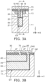
- FIGS. 3A and 3B are other schematic cross-sectional views showing the semiconductor device 1 according to the embodiment.
- FIG. 3A is a schematic view showing a cross-section of the gate trench GT at a contact region CA shown in FIG. 2 .
- FIG. 3B is a cross-sectional view along line A-A shown in FIG. 3A .
- the first interconnect 75 extends over the fourth insulating film 27 in a direction crossing the gate trenches GT.
- the first interconnect 75 is connected to the control electrode 40 via a contact hole CH1 provided in the fourth insulating film 27.
- control electrode 40 and the third electrode 50 extend in the Y-direction.
- the control electrode 40 is connected to the first interconnect 75 at the end portion of the control electrode 40; and the third electrode 50 is connected to the second interconnect 85 at the end portion of the third electrode 50.
- the third electrode 50 is drawn out to the same level as the front surface 10F of the semiconductor part 10 at the end of the gate trench GT; and the second interconnect 85 is connected to the third electrode 50 via a contact hole CH2 provided in the fourth insulating film 27.
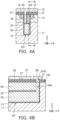
- FIGS. 4A and 4B are other schematic views showing a cross-section of the semiconductor device according to the embodiment.
- FIG. 4A is the same cross-sectional view as the cross-sectional view of the gate trench GT shown in FIG. 3A .
- FIG. 4B is a cross-sectional view along line B-B shown in FIG. 4A .
- the third electrode 50 is drawn out to the same level as the front surface 10F of the semiconductor part 10 at the end of the gate trench GT.
- the fourth electrode 60 is connected to a draw-out portion 50e of the third electrode 50 at the end of the gate trench GT.
- the second interconnect 85 is connected to the draw-out portion 50e of the third electrode 50 via the contact hole CH2 provided in the fourth insulating film 27.
- FIG. 5 is a time chart showing operations of the semiconductor device 1 according to the embodiment.
- the horizontal axis is a time T; and the vertical axis is gate voltages VG1, VG2, and VG3.
- Two examples of the gate control by the gate voltages VG1 to VG3 shown in FIG. 5 will now be described.
- the gate voltage VG1 is applied between the second electrode 30 and the first control pad 70.
- the gate voltage VG2 is applied between the second electrode 30 and the second control pad 80.
- the gate voltage VG1 is applied to the control electrode 40 via the first control pad 70.
- the gate voltage VG2 is applied to the third and fourth electrodes 50 and 60 via the second control pad 80.
- the gate voltage VG3 is applied to none of the control electrode 40, the third electrode 50, and the fourth electrode 60.
- the voltages of the control electrode 40, the third electrode 50, and the fourth electrode 60 are increased up to a level greater than the threshold voltage, for example, from -15 V to 15 V.
- the threshold voltage for example, from -15 V to 15 V.
- an inversion layer of the first conductivity type is induced at the interface between the first insulating film 21 and the second semiconductor layer 13 that faces the control electrode 40 and the fourth electrode 60; and the semiconductor device 1 transitions from the off-state to the on-state (i.e., turn-on).
- the voltage that is applied to the control electrode 40 is returned to -15 V, which is less than the threshold voltage.
- the voltages of the third and fourth electrodes 50 and 60 are returned to -15 V. Thereby, the inversion layer of the first conductivity type disappears at the interface between the second semiconductor layer 13 and the first insulating film 21.
- the semiconductor device 1 transitions from the on-state to the off-state (turns off) at which the inversion layer completely disappears at the interface between the second semiconductor layer 13 and the first insulating film 21. Moreover, at the time T3 directly before the time T2, an inversion layer of the second conductivity type is induced at the interface between the first insulating film 21 and the first semiconductor layer 11 that faces the third electrode 50. Thereby, the holes injected inside the first semiconductor layer 11 during the on-state can be ejected from the first semiconductor layer 11 to the second electrode 30 via the second semiconductor layer 13 before turn-off is started at the time T2; and the turn-off time can be reduced. The switching loss of the turn-off process of the semiconductor device 1 can be reduced thereby.
- the same bias as that applied to the third electrode 50 also is applied to the fourth electrode 60 so that the holes smoothly move to the second semiconductor layer 13 via the inversion layer of the second conductivity type induced at the interface between the first insulating film 21 and the first semiconductor layer 11. Moreover, the ejection resistance of the holes generated by the avalanche phenomenon in the first semiconductor layer 11 facing the bottom portion of the gate trench GT can be reduced thereby, and the avalanche resistance also can be improved.
- the semiconductor device 1 may be configured so that the third electrode 50 and the fourth electrode 60 are independently controlled.
- the fourth electrode 60 is not connected to the third electrode 50 and is electrically connected to a third control pad (not illustrated) other than the first and second control pads 70 and 80.
- the gate voltage VG1 is applied to the control electrode 40 via the first control pad 70.
- the gate voltage VG2 is applied to the fourth electrode 60 via the third control pad (not illustrated).
- the gate voltage VG3 is applied to the third electrode 50 via the second control pad 80.
- the voltages of the control electrode 40 and the fourth electrode 60 are increased from -15 V to 15 V.
- the voltage of the third electrode 50 is 0 V. Accordingly, the inversion layer of the first conductivity type is induced between the second semiconductor layer 13 and the first insulating film 21; and the semiconductor device 1 transitions from the off-state to the on-state.
- the third electrode 50 when the control electrode 40 and the fourth electrode 60 are turned on at the time T1, the third electrode 50 has the same potential as the fourth electrode 60.
- the potential of the third electrode 50 rises from -15 V to 15 V in the turn-on operation.
- a second conductivity type inversion layer is induced at the interface between the first semiconductor layer 11 and the first insulating film 21.
- the potential of the third electrode 50 rises and becomes a positive potential, a first conductivity type accumulation layer is formed after the p-type inversion layer disappears.
- the voltage of the third electrode 50 is 0 V, and neither a p-type inversion layer nor an n-type accumulation layer is induced. Therefore, the carrier flow that passes through the first semiconductor layer 11 proximate to the first insulating film 21 can be stabilized, and the turn-on characteristics can be stabilized.
- the gate voltage VG1 is reduced from 15 V to -15 V at the time T2; and the turn-off process is started thereby.
- the gate voltage VG2 is reduced from 15 V to -15 V
- the gate voltage VG3 is reduced from 0 V to -15 V.
- uniform electric field is provided by providing the third electrodes 50 respectively in the bottom portions of the gate trenches GT.
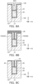
- FIGS. 6A to 8C are schematic cross-sectional views showing manufacturing processes of the semiconductor device 1 according to the embodiment.
- FIGS. 6A to 8C show a method of forming the control electrode 40, the third electrode 50, and the fourth electrode 60 in the gate trench GT.
- the gate trench GT is formed in a front surface 100F side of a semiconductor wafer 100.
- the semiconductor wafer 100 is, for example, n-type silicon.
- the gate trench GT is formed by selectively removing the semiconductor wafer 100 using an etching mask (not illustrated).
- the semiconductor wafer 100 is removed using anisotropic RIE (Reactive Ion Etching).
- the first insulating film 21 is formed at the front surface 100F side of a semiconductor wafer 100.
- the first insulating film 21 covers the inner surface of the gate trench GT with a space that remains in the gate trench GT.
- the first insulating film 21 is, for example, a silicon oxide film.
- the first insulating film 21 is formed by thermal oxidation of the semiconductor wafer 100.
- a conductive film 103 is formed on the first insulating film 21.
- the space in the gate trench GT is filled with the conductive film 103.
- the conductive film 103 is, for example, a conductive polysilicon film.
- the conductive film 103 is formed using, for example, CVD (Chemical Vapor Deposition).
- the conductive film 103 is removed so that the portion thereof remains at the bottom of the gate trench GT.
- a first space SP1 is formed at the upper portion of the gate trench GT.
- the conductive film 103 is removed using, for example, isotropic dry etching.
- the portion of the conductive film 103 that remains at the bottom of the gate trench GT becomes the third electrode 50.
- the second insulating film 23 is formed on the third electrode 50.
- the second insulating film 23 is, for example, a silicon oxide film.
- the second insulating film 23 is formed by, for example, thermal oxidation of the third electrode 50.
- a conductive film 105 is formed on the semiconductor wafer 100.
- the conductive film 105 covers the inner surface of the first space SP1.
- the conductive film 105 is formed so that a second space SP2 remains inside the gate trench GT.
- the conductive film 105 is, for example, a conductive polysilicon film.
- the conductive film 105 is formed using, for example, CVD.
- the conductive film 105 formed on the second insulating film 23 is partially removed so that the portion of the conductive film 105 remains on the inner wall of the gate trench GT.
- the conductive film 105 is removed via the second space SP2 using, for example, anisotropic RIE.
- the third insulating film 25 is formed on the semiconductor wafer 100.
- the second space SP2 is filled with the third insulating film 25.
- the third insulating film 25 is, for example, a silicon oxide film.
- the third insulating film 25 is formed using, for example, CVD.
- the third insulating film 25 and the conductive film 105 are removed so that the portion of the conductive film 105 remains inside the gate trench GT.
- the third insulating film 25 and the conductive film 105 are removed using, for example, isotropic dry etching or CMP (Chemical Mechanical Polishing).
- CMP Chemical Mechanical Polishing
- the manufacturing method described above is an example; and the embodiments are not limited thereto.
- the first space SP1 inside the gate trench GT may be filled with the conductive film 105.
- the second space SP2 may be formed by selective etching the conductive film 105 using an etching mask.
- FIGS. 9A and 9B are schematic cross-sectional views showing semiconductor devices 2 and 3 according to a first modification of the embodiment.
- the semiconductor device 2 includes the gate trenches GT1 and GT2 adjacent to each other; and a fourth electrodes 60 in the gate trench GT1 faces another fourth electrodes 60 in the gate trench GT2 via the second semiconductor layer 13.
- two control electrodes 40 may be configured to face each other via another second semiconductor layer 13.
- the positional relationship of the control electrode 40 and the fourth electrode 60 in an X-direction can be selected as appropriate.
- the third semiconductor layer 15 faces the control electrode 40 via the first insulating film 21; and the other third semiconductor layer 15 facing the fourth electrode 60 via the first insulating film (see FIG. 1 ) is not provided in this case.
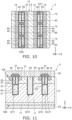
- FIG. 10 is a schematic plan view showing a semiconductor device 4 according to a second modification of the embodiment.
- FIG. 10 is a plan view showing the front surface 10F side of the semiconductor part 10.
- the second electrode 30 is not illustrated in FIG. 10 .
- multiple control electrodes 40 and multiple fourth electrodes 60 may be provided in one gate trench GT.
- the control electrodes 40 and the fourth electrodes 60 are provided on the third electrode 50 and alternately arranged in the Y-direction. In the X-direction, the control electrode 40 faces the fourth electrode 60.
- the embodiment is not limited to the example, and there may be a case where the fourth electrodes 60 face each other and the control electrodes 40 face each other with the second semiconductor layer 13 interposed.
- the third electrode 50 continuously extends in the Y-direction at the lower portion of the gate trench GT.
- the first interconnect 75 extends in the X-direction and is connected to the control electrode 40 via the contact hole CH1.
- the second interconnect 85 also extends in the X-direction and is connected to the fourth electrode 60 via the contact hole CH2.
- the first interconnect 75 and the second interconnect 85 are interlayer interconnects provided between the semiconductor part 10 and the second electrode 30.
- FIG. 11 is a schematic cross-sectional view showing a semiconductor device 5 according to a third modification of the embodiment.
- a third gate trench GT3 is further provided between the adjacent gate trench GT1 and gate trench GT2.
- the semiconductor device 5 further includes a fifth electrode 90 provided inside the gate trench GT3. Inside each of the gate trenches GT1 and GT2, the control electrode 40, the third electrode 50, and the fourth electrode 60 are provided.
- the gate trench GT3 extends into the first semiconductor layer 11 from the front surface 10F side of the semiconductor part 10.
- the fifth electrode 90 faces the first semiconductor layer 11 via a fifth insulating film 29.
- the fifth electrode 90 also faces the second semiconductor layer 13 via the fifth insulating film 29.
- the fifth electrode 90 is isolated from the semiconductor part by the fifth insulating film 29.
- the fifth electrode 90 is, for example, conductive polysilicon.
- the fifth electrode 90 may be electrically connected to the second electrode 30 or may be controlled independently from the other electrodes.
- the manufacturing method according to the embodiment is not limited to the example.
- at least one gate trench GT3 is provided between the gate trench GT1 and the gate trench GT2.
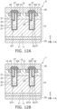
- FIGS. 12A and 12B are schematic cross-sectional views showing semiconductor devices 6 and 7 according to a fourth modification of the embodiment. As shown in FIGS. 12A and 12B , the semiconductor devices 6 and 7 is provided without the fourth electrode 60.
- the gate trench GT includes the control electrode 40 and the third electrode 50.
- the control electrode 40 is provided between the second electrode 30 and the third electrode 50.
- the third electrode 50 includes an extension portion 50f extending between the control electrode 40 and the second semiconductor layer 13.
- the control electrode 40 and the extension portion 50f of the third electrode 50 are arranged, for example, in the X-direction.
- the control electrode 40 faces the third electrode 50 via the second insulating film 23 and is electrically insulated from the third electrode 50 by the second insulating film 23.
- the control electrode 40 and the third electrode 50 are electrically insulated from the semiconductor part 10 by the first insulating film 21.
- the extension portion 50f of the third electrode 50 faces the second semiconductor layer 13 via the first insulating film 21.
- two third electrodes 50 provided respectively in two adjacent gate trenches GT1 and GT2 may include the extension portions 50f facing each other via the second semiconductor layer 13.
- the control electrode 40 in the gate trench GT1 or GT2 may face other control electrode 40 in other gate trench via other second semiconductor layer 13.
- an inversion layer of the second conductivity type also can be induced at the interface between the first insulating film 21 and the first semiconductor layer 11 facing the third electrode 50; and the hole ejection from the first semiconductor layer 11 to the second electrode 30 is promoted. Also, due to the extension portion 50f of the third electrode 50 extending between the control electrode 40 and the second semiconductor layer 13, the inversion layer of the second conductivity type is linked to the second semiconductor layer 13, and the holes are smoothly ejected thereto. The avalanche resistance can be further improved thereby.
- the semiconductor devices 6 and 7 may be configured to further include the fifth electrode 90 (see FIG. 11 ).
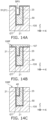
- FIGS. 13A to 14C are schematic cross-sectional views showing manufacturing processes of the semiconductor device 6 according to the fourth modification of the embodiment.
- FIGS. 13A to 14C show a method of forming the control electrode 40 and the third electrode 50 in the gate trench GT.
- the conductive film 103 is formed on the first insulating film 21.
- the gate trench GT is filled with the conductive film 103 (see FIGS. 6A to 6C ).
- the conductive film 103 is removed so that the portion thereof remains inside the gate trench GT.
- the conductive film 103 is removed using, for example, isotropic dry etching or CMP.
- an etching mask EM1 is formed at the front surface 100F side of the semiconductor wafer 100; and the conductive film 103 in the gate trench GT is partially removed. Thereby, a third space SP3 is formed inside the gate trench GT so that the remaining portion thereof becomes the third electrode 50.
- the first insulating film 21 may be partially removed through this process.
- the second insulating film 23 is formed by thermal oxidation of the third electrode 50.
- a sixth insulating film 31 is formed by thermal oxidation of the exposed portion in the semiconductor wafer 100.
- the sixth insulating film 31 is, for example, a silicon oxide film and is linked to the first insulating film 21 as a continuous body.
- the second insulating film 23 and the sixth insulating film 31 are formed so that the third space SP3 remains in the gate trench GT.
- a conductive film 107 is formed on the front surface 100F of the semiconductor wafer 100.
- the conductive film 107 is, for example, a conductive polysilicon film formed by CVD.
- the third space SP3 is filled with the conductive film 107.
- the conductive film 107 is partially removed on the front surface of the semiconductor wafer 100 and above the gate trench GT so that the portion thereof remains in the gate trench GT.
- the control electrode 40 is formed inside the third space SP3 (see FIG. 14A ).
- the conductive film 107 is removed using, for example, isotropic dry etching or CMP.
- the first insulating film 21 and the second insulating film 23 also are partially removed, and the upper surfaces of the front surface 100F of the semiconductor wafer 100, the control electrode 40, and the third electrode 50 are exposed.
- FIGS. 15A to 15D are schematic cross-sectional views showing semiconductor devices 8a, 8b, 9a and 9b according to a fifth modification of the embodiment.
- FIGS. 15A to 15D are plan views showing the front surface 10F side of the semiconductor part 10.
- the semiconductor devices 8a, 8b, 9a and 9b each include multiple control electrodes 40 and a fourth electrode 60.
- the fourth electrode 60 includes, for example, a first portion 60a and a second portion 60b.
- the fourth electrode 60 may be replaced by the third electrode 50.
- the first portion 60a and second portion 60b shown in FIGS. 15A to 15D may be an extension portion of the third electrode 50 (see the third electrode 50 in FIGS. 12A and 12B ).
- the multiple control electrodes 40 are apart from each other in the Y-direction.
- the first portion 60a is positioned between two adjacent control electrodes 40 in the Y-direction.
- the second portion 60b of the fourth electrode 60 extends, for example, in the Y-direction; and the control electrode 40 and the second portion 60b are arranged in the X-direction.
- the second portion 60b extends from the first portion 60a in the Y-direction or the opposite direction.
- the first portion 60a faces the second semiconductor layer 13 via the first insulating film 21 at the front surface 10F side of the semiconductor part 10.
- the third semiconductor layer 15 faces the control electrode 40 via the first insulating film 21.
- Another third semiconductor layer 15 faces the second portion 60b of the fourth electrode 60 via the first insulating film 21.
- the third semiconductor layer 15 and the other third semiconductor layer 15 are arranged in the X-direction; and the control electrode 40 and the second portion 60b of the fourth electrode 60 are arranged between the third semiconductor layer 15 and the other third semiconductor layer 15.
- the third semiconductor layer 15 is provided without facing the first portion 60a of the fourth electrode 60.
- the third semiconductor layer 15 faces the control electrode 40 via the first insulating film 21, and is provided without facing the fourth electrode 60 via the first insulating film 21.
- control electrode 40 and the second portion 60b of the fourth electrode 60 are arranged in the Y-direction with the first portion 60a of the fourth electrode 60 interposed. Also, the control electrode 40 and the second portion 60b of the fourth electrode 60 are arranged in the X-direction.
- the second portion 60b extends from the first portion 60a in the Y-direction or the opposite direction.
- the first portion 60a faces the second semiconductor layer 13 via the first insulating film 21 at the front surface 10F of the semiconductor part 10.
- the third semiconductor layer 15 faces the control electrode 40 via the first insulating film 21. Also, another third semiconductor layer 15 faces the second portion 60b of the fourth electrode 60 via the first insulating film 21.
- the third semiconductor layer 15 and the other third semiconductor layer 15 are arranged in the X-direction; and the control electrode 40 and the second portion 60b of the fourth electrode 60 are arranged between the third semiconductor layer 15 and the other third semiconductor layer 15.
- the third semiconductor layer 15 is provided without facing the first portion 60a of the fourth electrode 60.
- the third semiconductor layer 15 faces the control electrode 40 via the first insulating film 21, and is provided without facing the fourth electrode 60 via the first insulating film 21.
- the semiconductor device includes the following aspects:
Landscapes
- Electrodes Of Semiconductors (AREA)
Abstract
A semiconductor device (1 to 5, 8a, 8b, 9a, 9b) includes a semiconductor part (10), first to fourth electrodes (20, 30, 50, 60) and a control electrode (40). The first and second electrodes (20. 30) are provided respectively on back and front surfaces (10B, 10F) of the semiconductor part (10). The third electrode (50) is provided between the first and second electrodes (20, 30), and provided in the semiconductor part (10) with a first insulating film (21) interposed. The fourth and control electrodes (60, 40) are provided between the second and third electrodes (30, 50). The fourth and control electrodes (60, 40) extends into the semiconductor part (10) from the front side (10F) and faces the third electrode (50) with a second insulating film (23) interposed. The fourth electrode (60) is positioned between the semiconductor part (10) and the control electrode (40). The first insulating film (21) extends between the semiconductor part (10) and the control electrode (40) and between the semiconductor part (10) and the fourth electrode (60). The fourth electrode (60) faces the control electrode (40) with a third insulating film (25) interposed, and is electrically connected to the third electrode (50).
Description
- Embodiments relate to a semiconductor device.
- It is required for a power control semiconductor device to reduce the switching loss and increase the breakdown immunity.
-
-
FIG. 1 is a schematic cross-sectional view showing a semiconductor device according to an embodiment; -
FIG. 2 is a schematic plan view showing the semiconductor device according to the embodiment; -
FIGS. 3A and 3B are other schematic cross-sectional views showing the semiconductor device according to the embodiment; -
FIGS. 4A and 4B are yet other schematic cross-sectional views showing the semiconductor device according to the embodiment; -
FIG. 5 is a time chart showing operations of the semiconductor device according to the embodiment; -
FIGS. 6A to 8C are schematic cross-sectional views showing manufacturing processes of the semiconductor device according to the embodiment; -
FIGS. 9A and 9B are schematic cross-sectional views showing semiconductor devices according to a first modification of the embodiment; -
FIG. 10 is a schematic plan view showing a semiconductor device according to a second modification of the embodiment; -
FIG. 11 is a schematic cross-sectional view showing a semiconductor device according to a third modification of the embodiment; -
FIGS. 12A and 12B are schematic cross-sectional views showing semiconductor devices according to a fourth modification of the embodiment; -
FIGS. 13A to 14C are schematic cross-sectional views showing manufacturing processes of the semiconductor device according to the fourth modification of the embodiment; and -
FIGS. 15A to 15D are schematic cross-sectional views showing semiconductor devices according to a fifth modification of the embodiment. - According to one embodiment, a semiconductor device includes a semiconductor part, first to fourth electrodes and a control electrode. The first electrode is provided on a back surface of the semiconductor part; and the second electrode is provided on a front surface of the semiconductor part at a side opposite to the back surface. The third electrode is provided between the first electrode and the second electrode, and provided in the semiconductor part with a first insulating film interposed. The third electrode is electrically insulated from the semiconductor part by the first insulating film. The control electrode is provided between the second electrode and the third electrode. The control electrode extends into the semiconductor part from the front side of the semiconductor part and faces the third electrode with a second insulating film interposed. The first insulating film extends between the semiconductor part and the control electrode and electrically insulates the control electrode from the semiconductor part. The fourth electrode is provided between the second electrode and the third electrode. The fourth electrode extends into the semiconductor part from the front side of the semiconductor part and is positioned between the semiconductor part and the control electrode. The first insulating film extends between the semiconductor part and the fourth electrode; and the second insulating film extends between the third electrode and the fourth electrode. The fourth electrode faces the control electrode with a third insulating film interposed; and the fourth electrode is electrically connected to the third electrode.
- Embodiments will now be described with reference to the drawings. The same portions inside the drawings are marked with the same numerals; a detailed description is omitted as appropriate; and the different portions are described. The drawings are schematic or conceptual; and the relationships between the thicknesses and widths of portions, the proportions of sizes between portions, etc., are not necessarily the same as the actual values thereof. The dimensions and/or the proportions may be illustrated differently between the drawings, even in the case where the same portion is illustrated.
- There are cases where the dispositions of the components are described using the directions of XYZ axes shown in the drawings. The X-axis, the Y-axis, and the Z-axis are orthogonal to each other. Hereinbelow, the directions of the X-axis, the Y-axis, and the Z-axis are described as an X-direction, a Y-direction, and a Z-direction. Also, there are cases where the Z-direction is described as upward and the direction opposite to the Z-direction is described as downward.
-
FIG. 1 is a schematic cross-sectional view showing asemiconductor device 1 according to an embodiment. Thesemiconductor device 1 is, for example, an IGBT (Insulated Gate Bipolar Transistor). - As shown in
FIG. 1 , thesemiconductor device 1 includes asemiconductor part 10, afirst electrode 20, asecond electrode 30, acontrol electrode 40, athird electrode 50, and afourth electrode 60. Thesemiconductor part 10 is, for example, silicon. - The
semiconductor part 10 is provided between thefirst electrode 20 and thesecond electrode 30. Thefirst electrode 20 is, for example, a collector electrode and is provided on aback surface 10B of thesemiconductor part 10. Thesecond electrode 30 is, for example, an emitter electrode and is provided on afront surface 10F of thesemiconductor part 10 at the side opposite to theback surface 10B. - The
control electrode 40, thethird electrode 50, and thefourth electrode 60 are positioned, for example, between thefirst electrode 20 and thesecond electrode 30. Thesemiconductor part 10 includes, for example, a gate trench GT provided at thefront surface 10F side. Thecontrol electrode 40, thethird electrode 50, and thefourth electrode 60 are provided in the gate trench GT. - The
control electrode 40 is, for example, a gate electrode. Thecontrol electrode 40 extends into thesemiconductor part 10 from thefront surface 10F side of thesemiconductor part 10. Thecontrol electrode 40 is electrically insulated from thesemiconductor part 10 by a firstinsulating film 21. The firstinsulating film 21 is, for example, a gate insulating film. - The
third electrode 50 is provided inside thesemiconductor part 10 and is electrically insulated from thesemiconductor part 10 by, for example, the firstinsulating film 21. The firstinsulating film 21 extends between thesemiconductor part 10 and thethird electrode 50. Thethird electrode 50 is positioned between thefirst electrode 20 and thecontrol electrode 40. Thecontrol electrode 40 is provided between thesecond electrode 30 and thethird electrode 50. Thecontrol electrode 40 faces thethird electrode 50 via a secondinsulating film 23. Thecontrol electrode 40 is electrically insulated from thethird electrode 50 by the secondinsulating film 23. - The
fourth electrode 60 also extends into thesemiconductor part 10 from thefront surface 10F side of thesemiconductor part 10. Thefourth electrode 60 is provided between thesecond electrode 30 and thethird electrode 50. The second insulatingfilm 23 extends between thethird electrode 50 and thefourth electrode 60; and thefourth electrode 60 faces thethird electrode 50 via the second insulatingfilm 23. - The
fourth electrode 60 is positioned between thesemiconductor part 10 and thecontrol electrode 40. The first insulatingfilm 21 extends between thesemiconductor part 10 and thefourth electrode 60 and electrically insulates thefourth electrode 60 from thesemiconductor part 10. Thefourth electrode 60 faces thecontrol electrode 40 via a third insulatingfilm 25. Thefourth electrode 60 is electrically insulated from thecontrol electrode 40 by the third insulatingfilm 25. Thefourth electrode 60 is electrically connected to the third electrode 50 (seeFIG. 4B ). - The
control electrode 40 and thefourth electrode 60 are electrically insulated from thesecond electrode 30 by a fourth insulatingfilm 27. The fourth insulatingfilm 27 is, for example, an inter-layer insulating film. Thethird electrode 50 and thefourth electrode 60 serve as, for example, a second control electrode. - As shown in
FIG. 1 , thesemiconductor part 10 includes afirst semiconductor layer 11 of a first conductivity type, asecond semiconductor layer 13 of a second conductivity type, athird semiconductor layer 15 of the first conductivity type, and afourth semiconductor layer 17 of the second conductivity type. Hereinbelow, the first conductivity type is described as an n-type and the second conductivity type is described as a p-type, but the embodiments are not limited thereto. - The
first semiconductor layer 11 is, for example, an n-type base layer. Thefirst semiconductor layer 11 extends between thefirst electrode 20 and thesecond electrode 30. Thethird electrode 50 is positioned inside thefirst semiconductor layer 11 and faces thefirst semiconductor layer 11 via the first insulatingfilm 21. - The
second semiconductor layer 13 is, for example, a p-type base layer. Thesecond semiconductor layer 13 is provided between thefirst semiconductor layer 11 and thesecond electrode 30. Thesecond semiconductor layer 13 faces thecontrol electrode 40 via the first insulatingfilm 21. - As shown in
FIG. 1 , thesemiconductor part 10 further includes anothersecond semiconductor layer 13; and thecontrol electrode 40 and thefourth electrode 60 are positioned between thesecond semiconductor layer 13 and the othersecond semiconductor layer 13. The othersecond semiconductor layer 13 faces thefourth electrode 60 via the first insulatingfilm 21. - The
third semiconductor layer 15 is, for example, an n-type emitter layer. Thethird semiconductor layer 15 is provided between thesecond semiconductor layer 13 and thesecond electrode 30; and is partially provided on thesecond semiconductor layer 13. Thethird semiconductor layer 15 contacts the first insulatingfilm 21. - The
second electrode 30 covers the fourth insulatingfilm 27 and thefront surface 10F of thesemiconductor part 10. Thesecond electrode 30 is electrically connected to the second and third semiconductor layers 13 and 15 at, for example, thefront surface 10F of thesemiconductor part 10. - The
fourth semiconductor layer 17 is, for example, a p-type collector layer. Thefourth semiconductor layer 17 is provided between thefirst semiconductor layer 11 and thefirst electrode 20. Thefirst electrode 20 is in contact with, for example, thefourth semiconductor layer 17 and electrically connected thereto. -
FIG. 2 is a schematic plan view showing thesemiconductor device 1 according to the embodiment.FIG. 2 is a plan view showing thefront surface 10F side of thesemiconductor part 10. - As shown in
FIG. 2 , thesecond electrode 30, afirst control pad 70, asecond control pad 80, afirst interconnect 75, and asecond interconnect 85 are provided at thefront surface 10F side of thesemiconductor part 10. Thefirst control pad 70 and thesecond control pad 80 are apart from each other and are apart from thesecond electrode 30. Thefirst control pad 70, thesecond control pad 80, thefirst interconnect 75, and thesecond interconnect 85 are provided on thefront surface 10F of thesemiconductor part 10 with, for example, the fourth insulatingfilm 27 interposed. - The gate trench GT extends in, for example, a Y-direction below the
second electrode 30. Each of thecontrol electrode 40, thethird electrode 50, and thefourth electrode 60, for example, continuously extends in the Y-direction in the gate trench GT. - The
first control pad 70 is electrically connected to thecontrol electrode 40 via the first interconnect 75 (seeFIG. 3B ). Thesecond control pad 80 is electrically connected to the third andfourth electrodes FIG. 4B ). Thefirst control pad 70 and thefirst interconnect 75 are electrically insulated from thesecond control pad 80 and thesecond interconnect 85. -
FIGS. 3A and 3B are other schematic cross-sectional views showing thesemiconductor device 1 according to the embodiment.FIG. 3A is a schematic view showing a cross-section of the gate trench GT at a contact region CA shown inFIG. 2 .FIG. 3B is a cross-sectional view along line A-A shown inFIG. 3A . - As shown in
FIG. 3A , thefirst interconnect 75 extends over the fourth insulatingfilm 27 in a direction crossing the gate trenches GT. Thefirst interconnect 75 is connected to thecontrol electrode 40 via a contact hole CH1 provided in the fourth insulatingfilm 27. - As shown in
FIG. 3B , thecontrol electrode 40 and thethird electrode 50 extend in the Y-direction. Thecontrol electrode 40 is connected to thefirst interconnect 75 at the end portion of thecontrol electrode 40; and thethird electrode 50 is connected to thesecond interconnect 85 at the end portion of thethird electrode 50. Thethird electrode 50 is drawn out to the same level as thefront surface 10F of thesemiconductor part 10 at the end of the gate trench GT; and thesecond interconnect 85 is connected to thethird electrode 50 via a contact hole CH2 provided in the fourth insulatingfilm 27. -
FIGS. 4A and 4B are other schematic views showing a cross-section of the semiconductor device according to the embodiment.FIG. 4A is the same cross-sectional view as the cross-sectional view of the gate trench GT shown inFIG. 3A .FIG. 4B is a cross-sectional view along line B-B shown inFIG. 4A . - As shown in
FIG. 4B , thethird electrode 50 is drawn out to the same level as thefront surface 10F of thesemiconductor part 10 at the end of the gate trench GT. Thefourth electrode 60 is connected to a draw-outportion 50e of thethird electrode 50 at the end of the gate trench GT. Thesecond interconnect 85 is connected to the draw-outportion 50e of thethird electrode 50 via the contact hole CH2 provided in the fourth insulatingfilm 27. -
FIG. 5 is a time chart showing operations of thesemiconductor device 1 according to the embodiment. The horizontal axis is a time T; and the vertical axis is gate voltages VG1, VG2, and VG3. Two examples of the gate control by the gate voltages VG1 to VG3 shown inFIG. 5 will now be described. - The gate voltage VG1 is applied between the
second electrode 30 and thefirst control pad 70. The gate voltage VG2 is applied between thesecond electrode 30 and thesecond control pad 80. The gate voltage VG1 is applied to thecontrol electrode 40 via thefirst control pad 70. The gate voltage VG2 is applied to the third andfourth electrodes second control pad 80. In the example, the gate voltage VG3 is applied to none of thecontrol electrode 40, thethird electrode 50, and thefourth electrode 60. - As shown in
FIG. 5 , at a time T1, the voltages of thecontrol electrode 40, thethird electrode 50, and thefourth electrode 60 are increased up to a level greater than the threshold voltage, for example, from -15 V to 15 V. Thereby, an inversion layer of the first conductivity type is induced at the interface between the first insulatingfilm 21 and thesecond semiconductor layer 13 that faces thecontrol electrode 40 and thefourth electrode 60; and thesemiconductor device 1 transitions from the off-state to the on-state (i.e., turn-on). At a time T2 after the time T1, the voltage that is applied to thecontrol electrode 40 is returned to -15 V, which is less than the threshold voltage. At a time T3 that is after the time T1 and directly before the time T2, the voltages of the third andfourth electrodes second semiconductor layer 13 and the first insulatingfilm 21. - At the time T2, the
semiconductor device 1 transitions from the on-state to the off-state (turns off) at which the inversion layer completely disappears at the interface between thesecond semiconductor layer 13 and the first insulatingfilm 21. Moreover, at the time T3 directly before the time T2, an inversion layer of the second conductivity type is induced at the interface between the first insulatingfilm 21 and thefirst semiconductor layer 11 that faces thethird electrode 50. Thereby, the holes injected inside thefirst semiconductor layer 11 during the on-state can be ejected from thefirst semiconductor layer 11 to thesecond electrode 30 via thesecond semiconductor layer 13 before turn-off is started at the time T2; and the turn-off time can be reduced. The switching loss of the turn-off process of thesemiconductor device 1 can be reduced thereby. - In the example, the same bias as that applied to the
third electrode 50 also is applied to thefourth electrode 60 so that the holes smoothly move to thesecond semiconductor layer 13 via the inversion layer of the second conductivity type induced at the interface between the first insulatingfilm 21 and thefirst semiconductor layer 11. Moreover, the ejection resistance of the holes generated by the avalanche phenomenon in thefirst semiconductor layer 11 facing the bottom portion of the gate trench GT can be reduced thereby, and the avalanche resistance also can be improved. - The
semiconductor device 1 may be configured so that thethird electrode 50 and thefourth electrode 60 are independently controlled. In other words, thefourth electrode 60 is not connected to thethird electrode 50 and is electrically connected to a third control pad (not illustrated) other than the first andsecond control pads - The gate voltage VG1 is applied to the
control electrode 40 via thefirst control pad 70. The gate voltage VG2 is applied to thefourth electrode 60 via the third control pad (not illustrated). The gate voltage VG3 is applied to thethird electrode 50 via thesecond control pad 80. - In the example, at the time T1, the voltages of the
control electrode 40 and thefourth electrode 60 are increased from -15 V to 15 V. At this time, the voltage of thethird electrode 50 is 0 V. Accordingly, the inversion layer of the first conductivity type is induced between thesecond semiconductor layer 13 and the first insulatingfilm 21; and thesemiconductor device 1 transitions from the off-state to the on-state. - According to the first control example, when the
control electrode 40 and thefourth electrode 60 are turned on at the time T1, thethird electrode 50 has the same potential as thefourth electrode 60. The potential of thethird electrode 50 rises from -15 V to 15 V in the turn-on operation. When thethird electrode 50 has the negative potential, a second conductivity type inversion layer is induced at the interface between thefirst semiconductor layer 11 and the first insulatingfilm 21. When the potential of thethird electrode 50 rises and becomes a positive potential, a first conductivity type accumulation layer is formed after the p-type inversion layer disappears. In contrast, in the second control example, the voltage of thethird electrode 50 is 0 V, and neither a p-type inversion layer nor an n-type accumulation layer is induced. Therefore, the carrier flow that passes through thefirst semiconductor layer 11 proximate to the first insulatingfilm 21 can be stabilized, and the turn-on characteristics can be stabilized. - Then, the gate voltage VG1 is reduced from 15 V to -15 V at the time T2; and the turn-off process is started thereby. At the time T3 directly before the time T2, the gate voltage VG2 is reduced from 15 V to -15 V, and the gate voltage VG3 is reduced from 0 V to -15 V. Thereby, a second conductivity type inversion layer is induced at the interface between the
first semiconductor layer 11 and the first insulatingfilm 21, and the hole ejection is promoted. Thereby, it is possible in thesemiconductor device 1 to reduce the switching loss of the turn-off process. - According to the embodiment, at the bottom portions of the multiple gate trenches GT, uniform electric field is provided by providing the
third electrodes 50 respectively in the bottom portions of the gate trenches GT. Thus, it is possible to avoid element breakdown by the locally concentrated avalanche current due to nonuniformity of the electric field between the bottom portions of the trench gates GT. - A method for manufacturing the
semiconductor device 1 will now be described with reference toFIGS. 6A to 8C. FIGS. 6A to 8C are schematic cross-sectional views showing manufacturing processes of thesemiconductor device 1 according to the embodiment. -
FIGS. 6A to 8C show a method of forming thecontrol electrode 40, thethird electrode 50, and thefourth electrode 60 in the gate trench GT. - As shown in
FIG. 6A , the gate trench GT is formed in afront surface 100F side of asemiconductor wafer 100. Thesemiconductor wafer 100 is, for example, n-type silicon. The gate trench GT is formed by selectively removing thesemiconductor wafer 100 using an etching mask (not illustrated). Thesemiconductor wafer 100 is removed using anisotropic RIE (Reactive Ion Etching). - As shown in
FIG. 6B , the first insulatingfilm 21 is formed at thefront surface 100F side of asemiconductor wafer 100. The first insulatingfilm 21 covers the inner surface of the gate trench GT with a space that remains in the gate trench GT. The first insulatingfilm 21 is, for example, a silicon oxide film. The first insulatingfilm 21 is formed by thermal oxidation of thesemiconductor wafer 100. - As shown in
FIG. 6C , aconductive film 103 is formed on the first insulatingfilm 21. The space in the gate trench GT is filled with theconductive film 103. Theconductive film 103 is, for example, a conductive polysilicon film. Theconductive film 103 is formed using, for example, CVD (Chemical Vapor Deposition). - As shown in
FIG. 7A , theconductive film 103 is removed so that the portion thereof remains at the bottom of the gate trench GT. A first space SP1 is formed at the upper portion of the gate trench GT. Theconductive film 103 is removed using, for example, isotropic dry etching. The portion of theconductive film 103 that remains at the bottom of the gate trench GT becomes thethird electrode 50. - As shown in
FIG. 7B , in the first space SP1, the second insulatingfilm 23 is formed on thethird electrode 50. The second insulatingfilm 23 is, for example, a silicon oxide film. The second insulatingfilm 23 is formed by, for example, thermal oxidation of thethird electrode 50. - As shown in
FIG. 7C , aconductive film 105 is formed on thesemiconductor wafer 100. Theconductive film 105 covers the inner surface of the first space SP1. Theconductive film 105 is formed so that a second space SP2 remains inside the gate trench GT. Theconductive film 105 is, for example, a conductive polysilicon film. Theconductive film 105 is formed using, for example, CVD. - As shown in
FIG. 8A , theconductive film 105 formed on the second insulatingfilm 23 is partially removed so that the portion of theconductive film 105 remains on the inner wall of the gate trench GT. Theconductive film 105 is removed via the second space SP2 using, for example, anisotropic RIE. - As shown in
FIG. 8B , the third insulatingfilm 25 is formed on thesemiconductor wafer 100. The second space SP2 is filled with the third insulatingfilm 25. The thirdinsulating film 25 is, for example, a silicon oxide film. The thirdinsulating film 25 is formed using, for example, CVD. - As shown in
FIG. 8C , the third insulatingfilm 25 and theconductive film 105 are removed so that the portion of theconductive film 105 remains inside the gate trench GT. The thirdinsulating film 25 and theconductive film 105 are removed using, for example, isotropic dry etching or CMP (Chemical Mechanical Polishing). The portion of theconductive film 105 that remains inside the gate trench GT becomes thecontrol electrode 40 and thefourth electrode 60. - The manufacturing method described above is an example; and the embodiments are not limited thereto. For example, in the process shown in
FIG. 7C , the first space SP1 inside the gate trench GT may be filled with theconductive film 105. Subsequently, the second space SP2 may be formed by selective etching theconductive film 105 using an etching mask. -
FIGS. 9A and 9B are schematic cross-sectional views showingsemiconductor devices - As shown in
FIG. 9A , thesemiconductor device 2 includes the gate trenches GT1 and GT2 adjacent to each other; and afourth electrodes 60 in the gate trench GT1 faces anotherfourth electrodes 60 in the gate trench GT2 via thesecond semiconductor layer 13. Also, twocontrol electrodes 40 may be configured to face each other via anothersecond semiconductor layer 13. Thus, the positional relationship of thecontrol electrode 40 and thefourth electrode 60 in an X-direction can be selected as appropriate. - As shown in
FIG. 9B , in thesemiconductor device 3, thethird semiconductor layer 15 faces thecontrol electrode 40 via the first insulatingfilm 21; and the otherthird semiconductor layer 15 facing thefourth electrode 60 via the first insulating film (seeFIG. 1 ) is not provided in this case. -
FIG. 10 is a schematic plan view showing asemiconductor device 4 according to a second modification of the embodiment.FIG. 10 is a plan view showing thefront surface 10F side of thesemiconductor part 10. Thesecond electrode 30 is not illustrated inFIG. 10 . - As shown in
FIG. 10 ,multiple control electrodes 40 and multiplefourth electrodes 60 may be provided in one gate trench GT. In the gate trench GT, thecontrol electrodes 40 and thefourth electrodes 60 are provided on thethird electrode 50 and alternately arranged in the Y-direction. In the X-direction, thecontrol electrode 40 faces thefourth electrode 60. The embodiment is not limited to the example, and there may be a case where thefourth electrodes 60 face each other and thecontrol electrodes 40 face each other with thesecond semiconductor layer 13 interposed. Thethird electrode 50 continuously extends in the Y-direction at the lower portion of the gate trench GT. - The
first interconnect 75 extends in the X-direction and is connected to thecontrol electrode 40 via the contact hole CH1. Thesecond interconnect 85 also extends in the X-direction and is connected to thefourth electrode 60 via the contact hole CH2. In such a case, thefirst interconnect 75 and thesecond interconnect 85 are interlayer interconnects provided between thesemiconductor part 10 and thesecond electrode 30. -
FIG. 11 is a schematic cross-sectional view showing asemiconductor device 5 according to a third modification of the embodiment. In thesemiconductor device 5, a third gate trench GT3 is further provided between the adjacent gate trench GT1 and gate trench GT2. - The
semiconductor device 5 further includes afifth electrode 90 provided inside the gate trench GT3. Inside each of the gate trenches GT1 and GT2, thecontrol electrode 40, thethird electrode 50, and thefourth electrode 60 are provided. - The gate trench GT3 extends into the
first semiconductor layer 11 from thefront surface 10F side of thesemiconductor part 10. Thefifth electrode 90 faces thefirst semiconductor layer 11 via a fifth insulatingfilm 29. Thefifth electrode 90 also faces thesecond semiconductor layer 13 via the fifth insulatingfilm 29. Thefifth electrode 90 is isolated from the semiconductor part by the fifth insulatingfilm 29. Thefifth electrode 90 is, for example, conductive polysilicon. Thefifth electrode 90 may be electrically connected to thesecond electrode 30 or may be controlled independently from the other electrodes. - The manufacturing method according to the embodiment is not limited to the example. In the
semiconductor device 5, at least one gate trench GT3 is provided between the gate trench GT1 and the gate trench GT2. -
FIGS. 12A and 12B are schematic cross-sectional views showingsemiconductor devices FIGS. 12A and 12B , thesemiconductor devices fourth electrode 60. - As shown in
FIG. 12A , the gate trench GT includes thecontrol electrode 40 and thethird electrode 50. Thecontrol electrode 40 is provided between thesecond electrode 30 and thethird electrode 50. Thethird electrode 50 includes anextension portion 50f extending between thecontrol electrode 40 and thesecond semiconductor layer 13. Thecontrol electrode 40 and theextension portion 50f of thethird electrode 50 are arranged, for example, in the X-direction. - The
control electrode 40 faces thethird electrode 50 via the second insulatingfilm 23 and is electrically insulated from thethird electrode 50 by the second insulatingfilm 23. Thecontrol electrode 40 and thethird electrode 50 are electrically insulated from thesemiconductor part 10 by the first insulatingfilm 21. Theextension portion 50f of thethird electrode 50 faces thesecond semiconductor layer 13 via the first insulatingfilm 21. - As shown in
FIG. 12B , twothird electrodes 50 provided respectively in two adjacent gate trenches GT1 and GT2 may include theextension portions 50f facing each other via thesecond semiconductor layer 13. Thecontrol electrode 40 in the gate trench GT1 or GT2 may faceother control electrode 40 in other gate trench via othersecond semiconductor layer 13. - In the
semiconductor devices film 21 and thefirst semiconductor layer 11 facing thethird electrode 50; and the hole ejection from thefirst semiconductor layer 11 to thesecond electrode 30 is promoted. Also, due to theextension portion 50f of thethird electrode 50 extending between thecontrol electrode 40 and thesecond semiconductor layer 13, the inversion layer of the second conductivity type is linked to thesecond semiconductor layer 13, and the holes are smoothly ejected thereto. The avalanche resistance can be further improved thereby. Thesemiconductor devices FIG. 11 ). -
FIGS. 13A to 14C are schematic cross-sectional views showing manufacturing processes of thesemiconductor device 6 according to the fourth modification of the embodiment.FIGS. 13A to 14C show a method of forming thecontrol electrode 40 and thethird electrode 50 in the gate trench GT. - As shown in
FIG. 13A , theconductive film 103 is formed on the first insulatingfilm 21. The gate trench GT is filled with the conductive film 103 (seeFIGS. 6A to 6C ). - As shown in
FIG. 13B , theconductive film 103 is removed so that the portion thereof remains inside the gate trench GT. Theconductive film 103 is removed using, for example, isotropic dry etching or CMP. - As shown in
FIG. 13C , an etching mask EM1 is formed at thefront surface 100F side of thesemiconductor wafer 100; and theconductive film 103 in the gate trench GT is partially removed. Thereby, a third space SP3 is formed inside the gate trench GT so that the remaining portion thereof becomes thethird electrode 50. The first insulatingfilm 21 may be partially removed through this process. - As shown in
FIG. 14A , the second insulatingfilm 23 is formed by thermal oxidation of thethird electrode 50. Also, a sixth insulatingfilm 31 is formed by thermal oxidation of the exposed portion in thesemiconductor wafer 100. The sixth insulatingfilm 31 is, for example, a silicon oxide film and is linked to the first insulatingfilm 21 as a continuous body. The second insulatingfilm 23 and the sixth insulatingfilm 31 are formed so that the third space SP3 remains in the gate trench GT. - As shown in
FIG. 14B , aconductive film 107 is formed on thefront surface 100F of thesemiconductor wafer 100. Theconductive film 107 is, for example, a conductive polysilicon film formed by CVD. The third space SP3 is filled with theconductive film 107. - As shown in
FIG. 14C , theconductive film 107 is partially removed on the front surface of thesemiconductor wafer 100 and above the gate trench GT so that the portion thereof remains in the gate trench GT. Thereby, thecontrol electrode 40 is formed inside the third space SP3 (seeFIG. 14A ). Theconductive film 107 is removed using, for example, isotropic dry etching or CMP. At this time, the first insulatingfilm 21 and the second insulatingfilm 23 also are partially removed, and the upper surfaces of thefront surface 100F of thesemiconductor wafer 100, thecontrol electrode 40, and thethird electrode 50 are exposed. -
FIGS. 15A to 15D are schematic cross-sectional views showingsemiconductor devices FIGS. 15A to 15D are plan views showing thefront surface 10F side of thesemiconductor part 10. - The
semiconductor devices multiple control electrodes 40 and afourth electrode 60. Thefourth electrode 60 includes, for example, afirst portion 60a and asecond portion 60b. Thefourth electrode 60 may be replaced by thethird electrode 50. Thefirst portion 60a andsecond portion 60b shown inFIGS. 15A to 15D may be an extension portion of the third electrode 50 (see thethird electrode 50 inFIGS. 12A and 12B ). - In the example shown in
FIGS. 15A and 15B , themultiple control electrodes 40 are apart from each other in the Y-direction. Thefirst portion 60a is positioned between twoadjacent control electrodes 40 in the Y-direction. Thesecond portion 60b of thefourth electrode 60 extends, for example, in the Y-direction; and thecontrol electrode 40 and thesecond portion 60b are arranged in the X-direction. In the plan view, thesecond portion 60b extends from thefirst portion 60a in the Y-direction or the opposite direction. Thefirst portion 60a faces thesecond semiconductor layer 13 via the first insulatingfilm 21 at thefront surface 10F side of thesemiconductor part 10. - As shown in
FIG. 15A , in thesemiconductor device 8a, thethird semiconductor layer 15 faces thecontrol electrode 40 via the first insulatingfilm 21. Anotherthird semiconductor layer 15 faces thesecond portion 60b of thefourth electrode 60 via the first insulatingfilm 21. Thethird semiconductor layer 15 and the otherthird semiconductor layer 15 are arranged in the X-direction; and thecontrol electrode 40 and thesecond portion 60b of thefourth electrode 60 are arranged between thethird semiconductor layer 15 and the otherthird semiconductor layer 15. Thethird semiconductor layer 15 is provided without facing thefirst portion 60a of thefourth electrode 60. - As shown in
FIG. 15B , in thesemiconductor device 8b, thethird semiconductor layer 15 faces thecontrol electrode 40 via the first insulatingfilm 21, and is provided without facing thefourth electrode 60 via the first insulatingfilm 21. - As shown in
FIGS. 15C and 15D , thecontrol electrode 40 and thesecond portion 60b of thefourth electrode 60 are arranged in the Y-direction with thefirst portion 60a of thefourth electrode 60 interposed. Also, thecontrol electrode 40 and thesecond portion 60b of thefourth electrode 60 are arranged in the X-direction. Thesecond portion 60b extends from thefirst portion 60a in the Y-direction or the opposite direction. Thefirst portion 60a faces thesecond semiconductor layer 13 via the first insulatingfilm 21 at thefront surface 10F of thesemiconductor part 10. - As shown in
FIG. 15C , in thesemiconductor device 9a, thethird semiconductor layer 15 faces thecontrol electrode 40 via the first insulatingfilm 21. Also, anotherthird semiconductor layer 15 faces thesecond portion 60b of thefourth electrode 60 via the first insulatingfilm 21. Thethird semiconductor layer 15 and the otherthird semiconductor layer 15 are arranged in the X-direction; and thecontrol electrode 40 and thesecond portion 60b of thefourth electrode 60 are arranged between thethird semiconductor layer 15 and the otherthird semiconductor layer 15. Thethird semiconductor layer 15 is provided without facing thefirst portion 60a of thefourth electrode 60. - As shown in
FIG. 15D , in asemiconductor device 9b, thethird semiconductor layer 15 faces thecontrol electrode 40 via the first insulatingfilm 21, and is provided without facing thefourth electrode 60 via the first insulatingfilm 21. - According to the embodiments, the semiconductor device includes the following aspects:
- Note 1: A semiconductor device, comprising:
- a semiconductor part;
- a first electrode provided on a back surface of the semiconductor part;
- a second electrode provided on a front surface of the semiconductor part at a side opposite to the back surface;
- a third electrode provided between the first electrode and the second electrode, the third electrode being provided in the semiconductor part with a first insulating film interposed and being electrically insulated from the semiconductor part by the first insulating film; and
- a control electrode provided between the second electrode and the third electrode, the control electrode extending into the semiconductor part from the front side of the semiconductor part and facing the third electrode with a second insulating film interposed, the first insulating film extending between the semiconductor part and the control electrode and electrically insulating the control electrode from the semiconductor part,
- the third electrode including an extension portion extending between the semiconductor part and the control electrode, the first insulating film extending between the semiconductor part and the extension portion, the control electrode facing the extension portion via the second insulating film.
- Note 2: The device according to
note 1, wherein the second electrode is provided on the control electrode and the extension portion of the third electrode with a fourth insulating film interposed; and the control electrode and the extending portion of the third electrode are electrically insulated from the second electrode by the fourth insulating film. - Note 3: The device according to
note - the first semiconductor layer being of a first conductivity type and extending between the first electrode and the second electrode, the third electrode facing the first semiconductor layer via the first insulating film,
- the second semiconductor layer being of a second conductivity type and provided between the first semiconductor layer and the second electrode, the second semiconductor layer facing the control electrode with the first insulating film interposed,
- the third semiconductor layer being of the first conductivity type and partially provided on the second semiconductor layer, the third semiconductor layer contacting the first insulating film between the second semiconductor layer and the second electrode,
- the fourth semiconductor layer being of the second conductivity type and provided between the first semiconductor layer and the first electrode.
- Note 4: The device according to
note 3, wherein the third semiconductor layer faces the control electrode with the first insulating film interposed. - Note 5: The device according to
note - Note 6: The device according to
note 5, wherein the fifth electrode is electrically connected to the second electrode. - Note 7: The device according to any one of
notes 1 to 6, further comprising a first control pad and a second control pad, wherein the first control pad is provided at the front side of the semiconductor part, the first control pad being apart from the second electrode and electrically connected to the control electrode via a first interconnect; and the second control pad is provided at the front side of the semiconductor part, the second control pad being apart from the second electrode and the first control pad and electrically connected to the third electrode via a second interconnect. - Note 8: The device according to any one of
notes 1 to 7, further comprising a second third-electrode and a second control electrode, wherein- the second third-electrode is provided between the first electrode and the second electrode, the second third-electrode being provided in the semiconductor part with a second first-insulating film interposed and being electrically insulated from the semiconductor part by the second first-insulating film;
- the second control electrode is provided between the second electrode and the second third-electrode, the second control electrode extending into the semiconductor part from the front side of the semiconductor part and facing the second third-electrode with a second second-insulating film interposed, the second first-insulating film extending between the semiconductor part and the second control electrode and electrically insulating the second control electrode from the semiconductor part;
- the second third-electrode includes a second extension portion extending between the semiconductor part and the second control electrode, the second first-insulating film extending between the semiconductor part and the second extension portion, the second control electrode facing the second extension portion via the second second-insulating film; and
- the second extension portion of the second third-electrode faces the extension portion of the third electrode via the semiconductor part.
- Note 9: The device according to any one of
notes 1 to 7, further comprising a second third-electrode and a second control electrode, wherein- the second third-electrode is provided between the first electrode and the second electrode, the second third-electrode being provided in the semiconductor part with a second first-insulating film interposed and being electrically insulated from the semiconductor part by the second first-insulating film;
- the second control electrode is provided between the second electrode and the second third-electrode, the second control electrode extending into the semiconductor part from the front side of the semiconductor part and facing the second third-electrode with a second second-insulating film interposed, the second first-insulating film extending between the semiconductor part and the second control electrode and electrically insulating the second control electrode from the semiconductor part;
- the second third-electrode includes a second extension portion extending between the semiconductor part and the second control electrode, the second first-insulating film extending between the semiconductor part and the second extension portion, the second control electrode facing the second extension portion via the second second-insulating film; and
- the second control electrode faces the control electrode via the semiconductor part.
- Note 10: The device according to any one of
notes 1 to 9, wherein the extension portion of the third electrode includes a first extension portion and a second extension portion, the second extension portion extending from the first extension portion in a plan view parallel to the front surface of the semiconductor part; and the second extension portion and the control electrode are arranged in a direction crossing the extension direction of the second extension portion. - While certain embodiments have been described, these embodiments have been presented by way of example only, and are not intended to limit the scope of the inventions. Indeed, the novel embodiments described herein may be embodied in a variety of other forms; furthermore, various omissions, substitutions and changes in the form of the embodiments described herein may be made without departing from the spirit of the inventions. The accompanying claims and their equivalents are intended to cover such forms or modifications as would fall within the scope and overview of the invention.
- It is explicitly stated that all features disclosed in the description and/or the claims are intended to be disclosed separately and independently from each other for the purpose of original disclosure as well as for the purpose of restricting the claimed invention independent of the composition of the features in the embodiments and/or the claims. It is explicitly stated that all value ranges or indications of groups of entities disclose every possible intermediate value or intermediate entity for the purpose of original disclosure as well as for the purpose of restricting the claimed invention, in particular as limits of value ranges.
Claims (12)
- A semiconductor device (1 to 5, 8a, 8b, 9a, 9b), comprising:a semiconductor part (10);a first electrode (20) provided on a back surface (10B) of the semiconductor part (10);a second electrode (30) provided on a front surface (10F) of the semiconductor part (10) at a side opposite to the back surface (10B);a third electrode (50) provided between the first electrode (20) and the second electrode (30), the third electrode (50) being provided in the semiconductor part (10) with a first insulating film (21) interposed, the third electrode (50) being electrically insulated from the semiconductor part (10) by the first insulating film (21);a control electrode (40) provided between the second electrode (30) and the third electrode (50), the control electrode (40) extending into the semiconductor part (10) from the front side (10F) of the semiconductor part (10) and facing the third electrode (50) with a second insulating film (23) interposed, the first insulating film (21) extending between the semiconductor part (10) and the control electrode (40) and electrically insulating the control electrode (40) from the semiconductor part (10); anda fourth electrode (60) provided between the second electrode (30) and the third electrode (50), the fourth electrode (60) extending into the semiconductor part (10) from the front side (10F) of the semiconductor part (10) and being positioned between the semiconductor part (10) and the control electrode (40), the first insulating film (21) extending between the semiconductor part (10) and the fourth electrode (60), the second insulating film (23) extending between the third electrode (50) and the fourth electrode (60), the fourth electrode (60) facing the control electrode (40) with a third insulating film (25) interposed, the fourth electrode (60) being electrically connected to the third electrode (50).
- The device (1 to 5, 8a, 8b, 9a, 9b) according to claim 1, whereinthe second electrode (30) is provided on the control electrode (40) and the fourth electrode (60) with a fourth insulating film (27) interposed, andthe control electrode (40) and the fourth electrode (60) is electrically insulated from the second electrode (30) by the fourth insulating film (27).
- The device (1 to 5, 8a, 8b, 9a, 9b) according to claim 1 or 2, whereinthe semiconductor part (10) includes first to fourth semiconductor layers (11, 13, 15, 17),the first semiconductor layer (11) being of a first conductivity type and extending between the first electrode (20) and the second electrode (30), the third electrode (50) facing the first semiconductor layer (11) via the first insulating film (21),the second semiconductor layer (13) being of a second conductivity type and provided between the first semiconductor layer (11) and the second electrode (30), the second semiconductor layer (13) facing the control electrode (40) with the first insulating film (21) interposed,the third semiconductor layer (15) being of the first conductivity type and partially provided on the second semiconductor layer (13), the third semiconductor layer (15) contacting the first insulating film (21) between the second semiconductor layer (13) and the second electrode (30),the fourth semiconductor layer (17) being of the second conductivity type and provided between the first semiconductor layer (11) and the first electrode (20).
- The device (1 to 5, 8a, 8b, 9a, 9b) according to claim 3, wherein the third semiconductor layer (15) faces the control electrode (40) with the first insulating film (21) interposed.
- The device (3, 8b, 9b) according to claim 4, wherein the third semiconductor layer (15) is provided on the second semiconductor layer (13) without facing the fourth electrode (60).
- The device (4) according to any one of claims 1 to 4, wherein a plurality of the control electrodes 40 and a plurality of the fourth electrodes are provided on the third electrode (50) and alternately arranged along the front side (10F) of the semiconductor part 10.
- The device (5) according to claim 3 or 4, further comprising:a fifth electrode (90) provided between the first electrode (20) and the second electrode (30), the fifth electrode (90) extending into the first semiconductor layer (11) from the front side (10F) of the semiconductor part (10) with a fifth insulating film (29) interposed, the fifth electrode (90) being isolated from the semiconductor part (10) by the fifth insulating film (29),the second and third semiconductor layers (13, 15) being provided between the control electrode (40) and the fifth electrode (90).
- The device (5) according to claim 7, wherein the fifth electrode (90) is electrically connected to the second electrode (30).
- The device (1 to 5, 8a, 8b, 9a, 9b) according to any one of claims 1 to 8, further comprising:a first control pad (70) provided at the front side (10F) of the semiconductor part (10), the first control pad (70) being apart from the second electrode (30) and electrically connected to the control electrode (40) via a first interconnect (75); anda second control pad (80) provided at the front side (10F) of the semiconductor part (10), the second control pad (80) being apart from the second electrode (30) and the first control pad (70) and electrically connected to the third electrode (50) via a second interconnect (85).
- The device (2) according to any one of claims 1 to 4, 9, further comprising:a second third-electrode (50) provided between the first electrode (20) and the second electrode (30), the second third-electrode (50) being provided in the semiconductor part (10) with a second first-insulating film (21) interposed and being electrically insulated from the semiconductor part (10) by the second first-insulating film (21);a second control electrode (40) provided between the second electrode (30) and the second third-electrode (50), the second control electrode (40) extending into the semiconductor part (10) from the front side (10F) of the semiconductor part (10) and facing the second third-electrode (50) with a second second-insulating film (23) interposed, the second first-insulating film (21) extending between the semiconductor part (10) and the second control electrode (40) and electrically insulating the second control electrode (40) from the semiconductor part (10); anda second fourth-electrode (60) provided between the second electrode (30) and the second third-electrode (50), the second fourth-electrode (60) extending into the semiconductor part (10) from the front side (10F) of the semiconductor part (10) and being positioned between the semiconductor part (10) and the second control electrode (40), the second first-insulating film (21) extending between the semiconductor part (10) and the second fourth-electrode (60), the second second-insulating film (23) extending between the second third-electrode (50) and the second fourth-electrode (60), the second fourth-electrode (60) facing the second control electrode (40) with a second thirdinsulating film (25) interposed and being electrically connected to the second third-electrode (50),the second fourth-electrode (60) facing the fourth electrode (60) via the semiconductor part (10).
- The device (2) according to any one of claims 1 to 4, 9, further comprising:a second third-electrode (50) provided between the first electrode (20) and the second electrode (30), the second third-electrode (50) being provided in the semiconductor part (10) with a second first-insulating film (21) interposed and being electrically insulated from the semiconductor part (10) by the second first-insulating film (21);a second control electrode (40) provided between the second electrode (30) and the second third-electrode (50), the second control electrode (40) extending into the semiconductor part (10) from the front side (10F) of the semiconductor part (10) and facing the second third-electrode (50) with a second second-insulating film (23) interposed, the second first-insulating film (21) extending between the semiconductor part (10) and the second control electrode (40) and electrically insulating the second control electrode (40) from the semiconductor part (10); anda second fourth-electrode (60) provided between the second electrode (30) and the second third-electrode (50), the second fourth-electrode (60) extending into the semiconductor part (10) from the front side (10F) of the semiconductor part (10) and being positioned between the semiconductor part (10) and the second control electrode (40), the second first-insulating film (21) extending between the semiconductor part (10) and the second fourth-electrode (60), the second second-insulating film (23) extending between the second third-electrode (50) and the second fourth-electrode (60), the second fourth-electrode (60) facing the second control electrode (40) with a second thirdinsulating film (25) interposed and being electrically connected to the second third-electrode (50),the second control electrode (40) facing the control electrode (40) via the semiconductor part (10).
- The device (8a, 8b, 9a, 9b) according to anyone of claims 1 to 11, whereinthe fourth electrode (60) includes a first portion (60a) and a second portion (60b), the second portion (60b) extending from the first portion (60a) in a plan view parallel to the front surface (10F) of the semiconductor part (10), andthe second portion (60b) of the fourth electrode (60) and the control electrode (40) are arranged in a direction (X) crossing an extension direction (Y) of the second portion (60b).
Applications Claiming Priority (1)
| Application Number | Priority Date | Filing Date | Title |
|---|---|---|---|
| JP2022149685A JP7788978B2 (en) | 2022-09-21 | 2022-09-21 | Semiconductor Devices |
Publications (1)
| Publication Number | Publication Date |
|---|---|
| EP4343855A1 true EP4343855A1 (en) | 2024-03-27 |
Family
ID=85415463
Family Applications (1)
| Application Number | Title | Priority Date | Filing Date |
|---|---|---|---|
| EP23159217.1A Withdrawn EP4343855A1 (en) | 2022-09-21 | 2023-02-28 | Semiconductor device |
Country Status (4)
| Country | Link |
|---|---|
| US (1) | US20240097012A1 (en) |
| EP (1) | EP4343855A1 (en) |
| JP (1) | JP7788978B2 (en) |
| CN (1) | CN117747646A (en) |
Citations (5)
| Publication number | Priority date | Publication date | Assignee | Title |
|---|---|---|---|---|
| US20140077278A1 (en) * | 2012-09-18 | 2014-03-20 | Kabushiki Kaisha Toshiba | Semiconductor device and manufacturing method of the same |
| US20140167145A1 (en) * | 2012-12-18 | 2014-06-19 | Kabushiki Kaisha Toshiba | Semiconductor device |
| CN105742346A (en) * | 2016-04-26 | 2016-07-06 | 电子科技大学 | Double split trench gate charge storage-type RC-IGBT and manufacturing method thereof |
| CN113838921A (en) * | 2021-09-23 | 2021-12-24 | 电子科技大学 | Three-dimensional groove charge storage type IGBT and manufacturing method thereof |
| US20220085201A1 (en) * | 2020-09-15 | 2022-03-17 | Kabushiki Kaisha Toshiba | Semiconductor device and manufacturing method for the same |
Family Cites Families (13)
| Publication number | Priority date | Publication date | Assignee | Title |
|---|---|---|---|---|
| US7514743B2 (en) * | 2005-08-23 | 2009-04-07 | Robert Kuo-Chang Yang | DMOS transistor with floating poly-filled trench for improved performance through 3-D field shaping |
| JP5627494B2 (en) * | 2011-02-09 | 2014-11-19 | 株式会社東芝 | Semiconductor device and manufacturing method thereof |
| US9281368B1 (en) * | 2014-12-12 | 2016-03-08 | Alpha And Omega Semiconductor Incorporated | Split-gate trench power MOSFET with protected shield oxide |
| JP2016152357A (en) * | 2015-02-18 | 2016-08-22 | 株式会社東芝 | Semiconductor device and semiconductor package |
| JP6424684B2 (en) * | 2015-03-10 | 2018-11-21 | サンケン電気株式会社 | Semiconductor device |
| US10388783B2 (en) * | 2016-02-17 | 2019-08-20 | Polar Semiconductor, Llc | Floating-shield triple-gate MOSFET |
| JP2020150185A (en) * | 2019-03-14 | 2020-09-17 | 株式会社東芝 | Semiconductor device |
| TW202038470A (en) * | 2019-04-10 | 2020-10-16 | 台灣茂矽電子股份有限公司 | Mosfet and manufacturing method thereof |
| US10950699B2 (en) * | 2019-08-05 | 2021-03-16 | Vishay-Siliconix, LLC | Termination for vertical trench shielded devices |
| JP7252860B2 (en) * | 2019-08-20 | 2023-04-05 | 株式会社東芝 | semiconductor equipment |
| JPWO2023032653A1 (en) * | 2021-09-03 | 2023-03-09 | ||
| JP7610492B2 (en) * | 2021-09-08 | 2025-01-08 | 株式会社東芝 | Semiconductor Device |
| JP7801977B2 (en) * | 2022-09-08 | 2026-01-19 | ルネサスエレクトロニクス株式会社 | Semiconductor Devices |
-
2022
- 2022-09-21 JP JP2022149685A patent/JP7788978B2/en active Active
- 2022-12-23 CN CN202211663929.3A patent/CN117747646A/en active Pending
-
2023
- 2023-02-28 US US18/115,617 patent/US20240097012A1/en active Pending
- 2023-02-28 EP EP23159217.1A patent/EP4343855A1/en not_active Withdrawn
Patent Citations (5)
| Publication number | Priority date | Publication date | Assignee | Title |
|---|---|---|---|---|
| US20140077278A1 (en) * | 2012-09-18 | 2014-03-20 | Kabushiki Kaisha Toshiba | Semiconductor device and manufacturing method of the same |
| US20140167145A1 (en) * | 2012-12-18 | 2014-06-19 | Kabushiki Kaisha Toshiba | Semiconductor device |
| CN105742346A (en) * | 2016-04-26 | 2016-07-06 | 电子科技大学 | Double split trench gate charge storage-type RC-IGBT and manufacturing method thereof |
| US20220085201A1 (en) * | 2020-09-15 | 2022-03-17 | Kabushiki Kaisha Toshiba | Semiconductor device and manufacturing method for the same |
| CN113838921A (en) * | 2021-09-23 | 2021-12-24 | 电子科技大学 | Three-dimensional groove charge storage type IGBT and manufacturing method thereof |
Also Published As
| Publication number | Publication date |
|---|---|
| CN117747646A (en) | 2024-03-22 |
| JP2024044260A (en) | 2024-04-02 |
| JP7788978B2 (en) | 2025-12-19 |
| US20240097012A1 (en) | 2024-03-21 |
Similar Documents
| Publication | Publication Date | Title |
|---|---|---|
| CN112673466B (en) | Semiconductor device | |
| US8981470B2 (en) | Semiconductor device and manufacturing method of the same | |
| US10903348B2 (en) | Semiconductor device | |
| US20110095360A1 (en) | Method and device including transistor component having a field electrode | |
| US7646062B2 (en) | Semiconductor device comprising buried wiring layer | |
| CN110828567B (en) | Semiconductor device | |
| CN112713187B (en) | Semiconductor device | |
| CN115064592B (en) | Shielded gate power transistor and method for manufacturing the same | |
| US9276095B2 (en) | Semiconductor device | |
| US8652906B2 (en) | Method for manufacturing a semiconductor device and semiconductor device | |
| CN117747647A (en) | Semiconductor device with a semiconductor device having a plurality of semiconductor chips | |
| CN119486225A (en) | Trench gate silicon carbide MOSFET device and manufacturing method thereof | |
| US20240097012A1 (en) | Semiconductor device | |
| JP2021158199A (en) | Semiconductor device | |
| US11955546B2 (en) | Semiconductor device and method for controlling same | |
| US9318589B2 (en) | Insulated gate bipolar transistor | |
| CN113497033B (en) | Semiconductor device and control method thereof | |
| JP6177300B2 (en) | Semiconductor device | |
| US10522620B2 (en) | Semiconductor device having a varying length conductive portion between semiconductor regions | |
| US20260107502A1 (en) | Semiconductor device and method for manufacturing | |
| JP2021145077A (en) | Semiconductor device | |
| US20240097024A1 (en) | Semiconductor device and method for manufacturing semiconductor device | |
| US20250203972A1 (en) | Semiconductor device | |
| CN118693075A (en) | Semiconductor devices | |
| JP5841693B2 (en) | Semiconductor device |
Legal Events
| Date | Code | Title | Description |
|---|---|---|---|
| PUAI | Public reference made under article 153(3) epc to a published international application that has entered the european phase |
Free format text: ORIGINAL CODE: 0009012 |
|
| STAA | Information on the status of an ep patent application or granted ep patent |
Free format text: STATUS: REQUEST FOR EXAMINATION WAS MADE |
|
| 17P | Request for examination filed |
Effective date: 20230228 |
|
| AK | Designated contracting states |
Kind code of ref document: A1 Designated state(s): AL AT BE BG CH CY CZ DE DK EE ES FI FR GB GR HR HU IE IS IT LI LT LU LV MC ME MK MT NL NO PL PT RO RS SE SI SK SM TR |
|
| STAA | Information on the status of an ep patent application or granted ep patent |
Free format text: STATUS: THE APPLICATION HAS BEEN WITHDRAWN |
|
| 18W | Application withdrawn |
Effective date: 20240612 |