EP4343836A2 - Electronic device and related tiled electronic device - Google Patents
Electronic device and related tiled electronic device Download PDFInfo
- Publication number
- EP4343836A2 EP4343836A2 EP23193386.2A EP23193386A EP4343836A2 EP 4343836 A2 EP4343836 A2 EP 4343836A2 EP 23193386 A EP23193386 A EP 23193386A EP 4343836 A2 EP4343836 A2 EP 4343836A2
- Authority
- EP
- European Patent Office
- Prior art keywords
- sensing element
- electronic device
- circuit structure
- layer
- disposed
- Prior art date
- Legal status (The legal status is an assumption and is not a legal conclusion. Google has not performed a legal analysis and makes no representation as to the accuracy of the status listed.)
- Withdrawn
Links
Images




Classifications
-
- G—PHYSICS
- G01—MEASURING; TESTING
- G01J—MEASUREMENT OF INTENSITY, VELOCITY, SPECTRAL CONTENT, POLARISATION, PHASE OR PULSE CHARACTERISTICS OF INFRARED, VISIBLE OR ULTRAVIOLET LIGHT; COLORIMETRY; RADIATION PYROMETRY
- G01J1/00—Photometry, e.g. photographic exposure meter
- G01J1/02—Details
- G01J1/04—Optical or mechanical part supplementary adjustable parts
- G01J1/0407—Optical elements not provided otherwise, e.g. manifolds, windows, holograms, gratings
- G01J1/0437—Optical elements not provided otherwise, e.g. manifolds, windows, holograms, gratings using masks, aperture plates, spatial light modulators, spatial filters, e.g. reflective filters
-
- H—ELECTRICITY
- H10—SEMICONDUCTOR DEVICES; ELECTRIC SOLID-STATE DEVICES NOT OTHERWISE PROVIDED FOR
- H10W—GENERIC PACKAGES, INTERCONNECTIONS, CONNECTORS OR OTHER CONSTRUCTIONAL DETAILS OF DEVICES COVERED BY CLASS H10
- H10W70/00—Package substrates; Interposers; Redistribution layers [RDL]
- H10W70/60—Insulating or insulated package substrates; Interposers; Redistribution layers
- H10W70/611—Insulating or insulated package substrates; Interposers; Redistribution layers for connecting multiple chips together
- H10W70/614—Insulating or insulated package substrates; Interposers; Redistribution layers for connecting multiple chips together the multiple chips being integrally enclosed
-
- G—PHYSICS
- G01—MEASURING; TESTING
- G01J—MEASUREMENT OF INTENSITY, VELOCITY, SPECTRAL CONTENT, POLARISATION, PHASE OR PULSE CHARACTERISTICS OF INFRARED, VISIBLE OR ULTRAVIOLET LIGHT; COLORIMETRY; RADIATION PYROMETRY
- G01J1/00—Photometry, e.g. photographic exposure meter
- G01J1/02—Details
- G01J1/04—Optical or mechanical part supplementary adjustable parts
- G01J1/0407—Optical elements not provided otherwise, e.g. manifolds, windows, holograms, gratings
- G01J1/0411—Optical elements not provided otherwise, e.g. manifolds, windows, holograms, gratings using focussing or collimating elements, i.e. lenses or mirrors; Aberration correction
-
- H—ELECTRICITY
- H10—SEMICONDUCTOR DEVICES; ELECTRIC SOLID-STATE DEVICES NOT OTHERWISE PROVIDED FOR
- H10W—GENERIC PACKAGES, INTERCONNECTIONS, CONNECTORS OR OTHER CONSTRUCTIONAL DETAILS OF DEVICES COVERED BY CLASS H10
- H10W90/00—Package configurations
-
- H—ELECTRICITY
- H10—SEMICONDUCTOR DEVICES; ELECTRIC SOLID-STATE DEVICES NOT OTHERWISE PROVIDED FOR
- H10F—INORGANIC SEMICONDUCTOR DEVICES SENSITIVE TO INFRARED RADIATION, LIGHT, ELECTROMAGNETIC RADIATION OF SHORTER WAVELENGTH OR CORPUSCULAR RADIATION
- H10F39/00—Integrated devices, or assemblies of multiple devices, comprising at least one element covered by group H10F30/00, e.g. radiation detectors comprising photodiode arrays
- H10F39/10—Integrated devices
- H10F39/103—Integrated devices the at least one element covered by H10F30/00 having potential barriers, e.g. integrated devices comprising photodiodes or phototransistors
-
- H—ELECTRICITY
- H10—SEMICONDUCTOR DEVICES; ELECTRIC SOLID-STATE DEVICES NOT OTHERWISE PROVIDED FOR
- H10W—GENERIC PACKAGES, INTERCONNECTIONS, CONNECTORS OR OTHER CONSTRUCTIONAL DETAILS OF DEVICES COVERED BY CLASS H10
- H10W40/00—Arrangements for thermal protection or thermal control
Definitions
- the present disclosure relates to an electronic device and a related tiled electronic device, and more particularly to an electronic device including a circuit structure and a sensing element.
- the present disclosure aims at providing an electronic device and a related tiled electronic device with the configuration and structural design that integrate the circuit structure and the sensing element, so that the elements with various functions may be integrated in the electronic device, thereby improving the configuration and space design of each element for the electronic device or the tiled electronic device.
- the electronic device includes a protective layer, a circuit structure, a sensing element and a control unit.
- the circuit structure is disposed on the protective layer and surrounds the sensing element.
- the control unit is disposed between the circuit structure and the protective layer and electrically connected to the sensing element.
- the protective layer surrounds the control unit and contacts a surface of the circuit structure.
- a tiled electronic device includes two electronic devices and a connection unit.
- the two electronic devices are disposed adjacent to each other, and each of the electronic devices includes a protective layer, a circuit structure, a sensing element and a control unit.
- the circuit structure is disposed on the protective layer and surrounds the sensing element.
- the control unit is disposed between the circuit structure and the protective layer and electrically connected to the sensing element.
- the protective layer surrounds the control unit and contacts a surface of the circuit structure.
- the connection unit is disposed on one side of the circuit structure of each of the two electronic devices and electrically connected to the circuit structures of the two electronic devices.
- first, second, third, etc. are used to describe elements, but they do not mean and represent that the element(s) have any previous ordinal numbers, nor do they represent the order of one element and another element, or the order of manufacturing methods.
- the ordinal numbers are used only to clearly discriminate an element with a certain name from another element with the same name.
- the claims and the description may not use the same terms. Accordingly, in the following description, a first constituent element may be a second constituent element in a claim.
- the electronic device of the present disclosure may include a semiconductor device, a package device, a display device, a light-emitting device, a backlight device, a solar cell, a sensing device, an antenna device, a vehicle device, or a high-frequency device, but not limited herein.
- the electronic device may include a bendable or flexible electronic device.
- the display device may include a non-self-emissive display device or a self-emissive display device.
- the antenna device may include a liquid-crystal type antenna device or an antenna device other than liquid-crystal type, and the sensing device may include a sensing device used for sensing capacitance, light, heat or ultrasonic waves, but not limited herein.
- the electronic device may include electronic elements such as passive elements and active elements, for example, capacitors, resistors, inductors, diodes, transistors, etc. It should be noted that the electronic device may be any arrangement and combination of the above, but not limited herein.
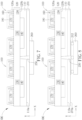
- FIG. 1 is a partial cross-sectional schematic diagram of an electronic device according to a first embodiment of the present disclosure.
- an electronic device 100 may include a protective layer 110, a circuit structure 120, a sensing element 130 and a control unit 140.
- the circuit structure 120 is disposed on the protective layer 110, and the circuit structure 120 surrounds the sensing element 130.
- the term "surround” referred in the present disclosure may mean that in a cross-sectional view of the electronic device 100, at least a portion of an element or layer that is surrounded is disposed in another element or layer, and in some embodiments, this another element or layer may further contact a side surface of the corresponding element or layer that is surrounded, but not limited herein.
- the circuit structure 120 may include a plurality of conductive layers 122 and a plurality of insulating layers 124 stacked in a direction Y, such as a conductive layer 122a, a conductive layer 122b, a conductive layer 122c, a conductive layer 122d, a conductive layer 122e, a conductive layer 122f, an insulating layer 124a, an insulating layer 124b, an insulating layer 124c, an insulating layer 124d and an insulating layer 124e, but not limited herein.
- the circuit structure 120 may be a redistribution layer (RDL), so as to redistribute the circuit.
- RDL redistribution layer
- the contact positions of the circuit may be changed or the fan-out area of the circuit may be increased through one or more metal wiring processes, but not limited herein.
- the direction Y may be a normal direction of the electronic device 100, which is opposite to a top-view direction of the electronic device 100, while a direction X may be parallel to a horizontal direction, which is parallel to a surface of the control unit 140 or the upper surface or lower surface of the protective layer 110, and the direction Y may be perpendicular to the direction X, but not limited herein.
- the conductive layer 122 may include metal materials such as titanium, copper, aluminum, tin, nickel, gold or silver or other suitable conductive materials.
- the conductive layer 122 may be a single metal layer or a stack of multiple metal layers.
- the insulating layer 124 may include organic materials or inorganic materials.
- the organic materials include, for example, polyimide (PI), photosensitive polyimide (PSPI), epoxy, Ajinomoto build-up film (ABF) or other suitable materials, but not limited herein.
- the inorganic materials include, for example, silicon oxide (SiOx), silicon nitride (SiNx) or other suitable materials, but not limited herein.
- the circuit structure 120 may further include active elements and/or passive elements, such as diodes, transistors, capacitors, resistors and/or inductors, which may be electrically connected to wires formed by the conductive layer 122.
- the transistor includes, for example, a thin film transistor (TFT), and the thin film transistor may include a gate, a source, a drain and a semiconductor layer, but not limited herein.
- the circuit structure 120 may be a thin-film array substrate or include a driving circuit, but not limited herein.
- the control unit 140 is disposed between the circuit structure 120 and the protective layer 110, and the control unit 140 is electrically connected to the sensing element 130.
- the term "disposed between" referred in the present disclosure may mean that portions of the elements overlap with each other in the direction X or the direction Y, whether that the whole layers or the whole surfaces of the elements are overlap with each other.
- the control unit 140 being disposed between the circuit structure 120 and the protective layer 110 may mean that the control unit 140, the circuit structure 120 and the protective layer 110 respectively have at least a portion overlapping with each other in the direction Y, and the arrangement of these overlapping portions in the direction Y is the protective layer 110, the control unit 140 and the circuit structure 120 in sequence.
- the protective layer 110 surrounds the control unit 140, and the protective layer 110 contacts a surface of the circuit structure 120.
- the control unit 140 is located within the protective layer 110, or the protective layer 110 is located at the periphery of the control unit 140 and surrounds the control unit 140. Therefore, in a direction parallel to the upper surface or lower surface of the protective layer 110 (e.g., in the direction X), the protective layer 110 is located at both sides of the control unit 140, as shown in the cross-sectional view of FIG. 1 .
- at least a portion of the control unit 140 may be disposed within the protective layer 110.
- the protective layer 110 may contact the side surface and/or the lower surface of the control unit 140.
- the protective layer 110 may cover the lower surface of the control unit 140. In other embodiments, the lower surface of the control unit 140 is not covered by the protective layer 110. For example, the protective layer 110 may expose the lower surface of the control unit 140 by a grinding process, but not limited herein.
- the control unit 140 may include, for example, a driver integrated circuit (driver IC) or other suitable units that are able to generate control signals or have control elements, but not limited herein. In some embodiments, the control unit 140 may be an integrated circuit chip, but not limited herein.
- the circuit structure 120 may include an upper surface 120a and a lower surface 120b opposite to the upper surface 120a.
- the lower surface 120b of the circuit structure 120 may face the control unit 140, and the protective layer 110 may contact the lower surface 120a of the circuit structure 120.
- the protective layer 110 may be used to reduce the influence of moisture.
- the protective layer 110 may include, for example, epoxy, ceramic, epoxy molding compound (EMC), other suitable materials or combinations of the above materials, but not limited herein.
- the sensing element 130 may be disposed in the circuit structure 120.
- the sensing element 130 may be integrally disposed in the circuit structure 120, and the circuit structure 120 may contact the side surface of the sensing element 130 (as shown in FIG. 1 ).
- the sensing element 130 may be partially disposed in the circuit structure 120, and the upper surface of the sensing element 130 is exposed (as shown in FIG. 6 ).
- the sensing element 130 may be, for example, a light sensor, a thermal sensor or a pressure sensor, and the light sensor includes, for example, a PIN diode, but not limited herein. In some embodiments, as shown in FIG.
- the sensing element 130 may include an upper surface 130a and a side surface 130b connected to the upper surface 130a, and the upper surface 130a is opposite to the control unit 140. Furthermore, the circuit structure 120 may contact the side surface 130b of the sensing element 130.
- the insulating layer 124 of the circuit structure 120 may contact the side surface 130b of the sensing element 130, and/or the insulating layer 124 of the circuit structure 120 may contact and cover the upper surface 130a of the sensing element 130.
- the insulating layer 124 may circularly surround the sensing element 130 and contact any portion of the side surface 130b of the sensing element 130, but not limited herein.
- the sensing element 130 and one of the conductive layers 122 of the circuit structure 120 may be disposed on the same insulating layer 124, that is, the sensing element 130 may be manufactured together with the circuit structure 120 to integrate the circuit structure 120 and the sensing element 130.
- a conductive layer 122a, an insulating layer 124a, a conductive layer 122b, an insulating layer 124b, a conductive layer 122c, an insulating layer 124c, a conductive layer 122d, an insulating layer 124d, a conductive layer 122e, an insulating layer 124e and a conductive layer 122f that are patterned may be alternately formed in sequence in the direction Y
- the conductive layer 122d may be formed on the insulating layer 124c
- the sensing element 130 may further be formed on the insulating layer 124c by, for example, an electroplating process, a thin-film process and/or a semiconductor process.
- the sensing element 130 and the conductive layer 122d may be disposed on the same insulating layer 124c, but not limited herein.
- the insulating layer 124a, the insulating layer 124b and the insulating layer 124c that are formed before forming the sensing element 130 may include inorganic materials for reducing the influence of the process temperature on the materials of the insulating layers, and the insulating layer 124d and the insulating layer 124e that are formed after forming the sensing element 130 may include organic materials, but not limited herein.
- the inorganic materials and the organic materials described above may be referred to the previous paragraphs, which will not be described redundantly herein.
- the insulating layer 124 of the circuit structure 120 may cover the sensing element 130.
- the insulating layer 124e may cover the upper surface 130a of the sensing element 130.
- the conductive layer 122 of the circuit structure 120 is not disposed above the sensing element 130, that is, there is no conductive layer 122 between the upper surface 130a of the sensing element 130 and the uppermost insulating layer 124e, so as to reduce the influence on the sensitivity or other electrical properties of the sensing element 130.
- the insulating layer 124 above the sensing element 130 may have a high light transmittance.
- the transmittance of the insulating layer 124 above the sensing element 130 may be greater than 70%, and the refractive index thereof may be greater than or equal to 1.1 and less than or equal to 1.6, which may, for example, prevent interface reflection, so as to improve the sensing quality of the sensing element 130, but not limited herein.
- the insulating layer 124 may have the function of an anti-reflective layer (AR layer), which may be a single layer or a stack of materials with different refractive indices, for example.
- AR layer anti-reflective layer
- the insulating layer 124 may have the function of a filter layer, which may allow light with a specific wavelength to pass through, so as to improve the sensing quality of the sensing element 130.
- a hole may be formed in the insulating layer 124 on the upper side of the sensing element 130, so that the circuit structure 120 may expose the upper surface 130a of the sensing element 130. Therefore, light L may directly enter the sensing element 130 from the outside, thereby improving the sensing quality of the sensing element 130, but not limited herein.
- the control unit 140 may be electrically connected to the sensing element 130 through the circuit structure 120.
- the control unit 140 may be electrically connected to an electrode of the sensing element 130 through the conductive layer 122a, the conductive layer 122b, the conductive layer 122c and the conductive layer 122d, but not limited herein.
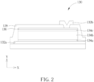
- the sensing element 130 may include a PIN diode, wherein FIG. 2 is a partial cross-sectional schematic diagram of a sensing element according to an embodiment of the present disclosure.
- the sensing element 130 may include, for example, a first electrode 132a, a first semiconductor layer 134a (e.g., an N-type semiconductor layer), a second semiconductor layer 134b (e.g., an intrinsic semiconductor layer), a third semiconductor layer 134c (e.g., a P-type semiconductor layer) and a transparent electrode 136 (e.g., an indium tin oxide (ITO) electrode) which are stacked in the direction Y, and the first electrode 132a may be electrically connected to the conductive layer 122d.
- the sensing element 130 may further include a second electrode 132b, and the second electrode 132b may further pass through a connection hole of an insulating layer 138 and be disposed on the insulating layer 138.
- the insulating layer 138 is disposed on the transparent electrode 136, and the second electrode 132b is electrically connected to the transparent electrode 136 through the connection hole in the insulating layer 138.
- the insulating layer 138 may be regarded as a portion of the sensing element 130, or the insulating layer 138 may be regarded as a portion of the insulating layer 124 in the circuit structure 120.
- the first electrode 132a and the second electrode 132b may include, for example, metal materials or composite conductive materials, but not limited herein.
- the circuit structure 120 may further include a patterned metal layer 150, the sensing element 130 is disposed on the patterned metal layer 150, and the patterned metal layer 150 may have a floating potential, but not limited herein.
- the patterned metal layer 150 may be disposed between the control unit 140 and the sensing element 130. In the normal direction Y of the electronic device 100, the patterned metal layer 150 may overlap the sensing element 130, such as completely shielding the lower surface of the sensing element 130, thereby reducing the influence of stray light on the sensing element 130.
- the patterned metal layer 150 may be replaced by a light-shielding layer.
- the light-shielding layer may include, for example, metal materials, black photoresist materials or other materials with good light reflectivity and/or light absorption, but not limited herein.
- the electronic device 100 may further include a light-shielding structure 160.
- the light-shielding structure 160 is disposed on the circuit structure 120 and has a plurality of openings 162, and one opening 162a of the plurality of openings 162 may correspond to the sensing element 130.
- the opening 162a of the light-shielding structure 160 exposes the sensing element 130. Further, the light-shielding structure 160 does not shield or overlap the sensing element 130 in the direction Y, so that the light L may enter the sensing element 130 through the opening 162a.
- the light-shielding structure 160 may include, for example, metal materials, black photoresist materials, opaque materials, organic materials or other materials with good light reflectivity and/or light absorption.
- the electronic device 100 may further include a function element 170, and the function element 170 is correspondingly disposed in another one opening 162b of the plurality of openings 162.
- the function element 170 may be electrically connected to the control unit 140 through the circuit structure 120.
- the control unit 140 may be electrically connected to an electrode 170e1 of the function element 170 through the conductive layer 122a, the conductive layer 122b, the conductive layer 122c, the conductive layer 122d, the conductive layer 122e and the conductive layer 122f.
- the function element 170 may be, for example, a light-emitting element, an antenna element or other elements with specific functions required according to the product.
- the light-emitting element may include, for example, a light-emitting diode (LED), which may generate light T emitting to the outside, but not limited herein.
- the light-shielding structure 160 may, for example, reduce the influence of the light T emitted by the function element 170 on the sensing element 130, thereby reducing the influence of stray light.
- the function element 170 may not overlap the sensing element 130 in the direction Y
- the electronic device 100 may include two function elements 170, which are respectively disposed in two openings 162b of the plurality of openings 162, and the sensing element 130 may be located between the two function elements 170 when viewed in the direction Y
- the number and arrangement of the function elements 170 and the corresponding openings 162b are not limited herein, which may be adjusted according to practical structural design of the device.
- the electronic device 100 may further include an encapsulant layer 180.
- the encapsulant layer 180 covers the function element 170 and the light-shielding structure 160, and the encapsulant layer 180 may expose the region where the sensing element 130 is located.
- the encapsulant layer 180 may have an opening 182 to expose a portion of the upper surface of the uppermost insulating layer 124e in the circuit structure 120.
- the opening 182 of the encapsulant layer 180 may correspond to the opening 162a of the light-shielding structure 160, and the size of the opening 182 may be less than the size of the opening 162a, but not limited herein.
- the encapsulant layer 180 may be, for example, a light-transmissive material, including epoxy, ceramic, other suitable materials or combinations of the above materials, but not limited herein.
- the sensing element 130 and the function element 170 may be electrically connected to the same control unit 140 through the circuit structure 120, so that the control unit 140 may drive the sensing element 130 and the function element 170 simultaneously or in a time-division manner. That is to say, the sensing element 130 and the function element 170 may share the control unit 140, so that elements with various functions such as the sensing element 130 and the function element 170 may be integrated in the electronic device 100, thereby reducing the number of required control units 140.
- control unit 140 may be electrically connected to the sensing elements 130 located in a plurality of regions through the circuit structure 120, or the control unit 140 may be electrically connected to the function elements 170 located in a plurality of regions through the circuit structure 120, but not limited herein.
- the manufacturing process of the electronic device 100 in the present disclosure may be, for example, a panel-level package (FOPLP) process, and may be a chip-first process or a RDL-first process, but not limited herein.
- FOPLP panel-level package
- FIG. 3 is a partial cross-sectional schematic diagram of an electronic device according to a second embodiment of the present disclosure, wherein the electronic device 100 shown in FIG. 3 may be manufactured by a chip-first process.
- the conductive layers in the circuit structure 120 are omitted in FIG. 3 and the following FIG. 4 , FIG. 5 and FIG. 7 to FIG. 10 , and the entirety of multiple insulating layers in the circuit structure 120 is represented by an insulating layer 124.
- an electronic device 100 may further include one or plural collimator(s) 200, and the collimator 200 may be disposed in one opening 162a of the plurality of openings 162 and correspond to the sensing element 130.
- the collimator 200 Through the design of the collimator 200, the function of collimating the light L may be provided for the sensing element 130.
- the light path of the light L entering the sensing element 130 may be approximately parallel to the normal direction Y, or have an included angle with the direction Y not greater than 60 degrees, not greater than 45 degrees or not greater than 30 degrees, thereby improving the accuracy of the sensing element 130.
- the collimator 200 has a first height h1
- the encapsulant layer 180 has a second height h2
- the first height h1 is less than or equal to the second height h2.
- a ratio of the first height h1 to the second height h2 i.e., h1/h2 may be greater than or equal to 0.1 and less than or equal to 1.
- the accuracy of the sensing element 130 may be improved or the cracking of the encapsulant layer 180 caused by the protruding collimator 200 may be reduced, but not limited herein.
- the collimator 200 does not overlap at least a portion of the sensing element 130.
- the collimator 200 may be disposed on the insulating layer 124 of the circuit structure 120, and the collimator 200 may be disposed in the opening 182 of the encapsulant layer 180.
- the opening 182 of the encapsulant layer 180 corresponds to the opening 162a of the light-shielding structure 160.
- the collimator 200 may include, for example, metal materials, black photoresist materials or other materials with good light reflectivity and/or light absorption, and the material of the collimator 200 may be the same as or different from the material of the light-shielding structure 160.
- the circuit structure 120 may further include a patterned metal layer 150, and the sensing element 130 is disposed on the patterned metal layer 150. By disposing the patterned metal layer 150 corresponding to the sensing element 130, the leakage current may be reduced.
- the patterned metal layer 150 has a floating potential, for example, but not limited herein.
- the protective layer 110 may be disposed around the control unit 140 to surround the control unit 140.
- the circuit structure 120 is formed on the protective layer 110 and electrically connected to conductive pads 142 on the active surface of the control unit 140.
- the sensing element 130 may be manufactured together with the circuit structure 120.
- the sensing element 130 is formed in the insulating layer 124 of the circuit structure 120 through a thin-film process and/or a semiconductor process.
- the light-shielding structure 160, the collimator 200, the function element 170 and the encapsulant layer 180 may be formed on the circuit structure 120 subsequently, but not limited herein.
- the order of forming the function element 170, the light-shielding structure 160 and the collimator 200 may be adjusted according to the process design, as well as in other embodiments, which will not be redundantly described.
- the sensing element 130 in order to reduce the influence of the high-temperature process of the sensing element 130 on the circuit structure 120, the sensing element 130 may be formed earlier, so that the sensing element 130 may be closer to the control unit 140. That is to say, the sensing element 130 may be closer to the lower surface 120b of the circuit structure 120 and farther away from the upper surface 120a of the circuit structure 120, but not limited herein.
- FIG. 4 is a partial cross-sectional schematic diagram of an electronic device according to a third embodiment of the present disclosure, wherein the electronic device 100 shown in FIG. 4 may be manufactured by a RDL-first process.
- the circuit structure 120 may expose the upper surface 130a of the sensing element 130.
- the upper surface 130a of the sensing element 130 may be aligned with the upper surface 120a of the circuit structure 120. Therefore, the light L may directly enter the sensing element 130 from the outside without passing through the insulating layer 124 of the circuit structure 120 first, thereby improving the sensing quality of the sensing element 130.
- the collimator 200 may be disposed in one opening 162a of the plurality of openings 162 of the light-shielding structure 160 and correspond to the sensing element 130.
- the collimator 200 may directly contact and be disposed on the upper surface 130a of the sensing element 130, but not limited herein.
- the collimator 200 may be disposed in the opening 182 of the encapsulant layer 180, and the opening 182 of the encapsulant layer 180 corresponds to the opening 162a of the light-shielding structure 160.
- a plurality of bonding elements 210 may be disposed between the circuit structure 120 and the control unit 140, and the circuit structure 120 may be electrically connected to the conductive pads 142 of the control unit 140 through the bonding elements 210.
- the bonding element 210 may be, for example, under-bump metallization (UBM), a bump, a solder ball or a pad.
- UBM under-bump metallization
- the bonding element 210 may include copper, tin, nickel, gold, lead, other suitable conductive materials or combinations of the above materials, but not limited herein.
- the circuit structure 120 may further include a light-shielding element 220, and the light-shielding element 220 may be disposed at at least one side of the sensing element 130.
- the light-shielding element 220 and the sensing element 130 do not overlap each other in the direction Y, or the sensing element 130 is disposed between two adjacent light-shielding elements 220.
- the light-shielding element 220 may surround the sensing element 130, but not limited herein.
- the light-shielding element 220 may include, for example, metal materials, black photoresist materials or other materials with good light reflectivity and/or light absorption.
- the light-shielding element 220 may reduce the influence of the light emitted by the function element 170 on the sensing element 130, or may reduce the influence of side light or stray light in the environment on the sensing element 130, but not limited herein.
- the circuit structure 120 and the sensing element 130 disposed in the circuit structure 120 may be formed first, so that the circuit structure 120 surrounds the sensing element 130.
- the bonding elements 210 may be formed when the circuit structure 120 is formed.
- the bonding elements 210 may be formed on the lower surface 120b of the circuit structure 120 or the upper surface of the control unit 140 when the control unit 140 is provided on the lower surface 120b of the circuit structure 120, so that the circuit structure 120 is electrically connected to the conductive pads 142 of the control unit 140 through the bonding elements 210, and then the protective layer 110 may be formed to surround the control unit 140.
- the light-shielding structure 160, the collimator 200, the function element 170 and the encapsulant layer 180 may be formed on the circuit structure 120 subsequently, but not limited herein.
- FIG. 5 is a partial cross-sectional schematic diagram of an electronic device according to a fourth embodiment and a variation embodiment thereof of the present disclosure.
- an electronic device 100 according to a fourth embodiment of the present disclosure may further include a lens 230, and the lens 230 is disposed in one opening 162a of the plurality of openings 162 and corresponds to the sensing element 130.
- the lens 230 may collimate or concentrate the light L, thereby improving the accuracy of the sensing element 130.
- the center of the lens 230 or the thickest portion of the lens 230 may substantially correspond to the center of the sensing element 130, but not limited herein.
- the lens 230 may be disposed on the insulating layer 124, and the lens 230 may be disposed in the opening 182 of the encapsulant layer 180.
- the opening 182 of the encapsulant layer 180 corresponds to the opening 162a of the light-shielding structure 160.
- the lens 230 further include a filter layer 232, so that the light L with a specific wavelength band enters the sensing element 130.
- the light L with a specific wavelength band may be, for example, infrared light, but not limited herein.
- FIG. 6 is a partial cross-sectional schematic diagram of an electronic device according to a fifth embodiment of the present disclosure.
- the circuit structure 120 may have a groove 126, and the sensing element 130 is disposed in the groove 126.
- the sensing element 130 may be a package element with a complete package structure.
- the sensing element 130 may be disposed in the groove 126 of the circuit structure 120, and a bonding element 240 may be further disposed between the circuit structure 120 and the sensing element 130.
- the sensing element 130 may be electrically connected to the conductive layer 122 of the circuit structure 120 through the bonding element 240, thereby being electrically connected to the control unit 140 through the conductive layer 122.
- the bonding element 240 may be, for example, a conductive adhesive or a conductive pad.
- the conductive adhesive includes, for example, an anisotropic conductive film (ACF), but not limited herein. When the conductive adhesive is used as the bonding element 240, the sensing element 130 may be fixed in the groove 126.
- the groove 126 may overlap the opening 162a of the light-shielding structure 160 in the direction Y, and the groove 126 may further overlap the opening 182 of the encapsulant layer 180 in the direction Y, so that the upper surface 130a of the sensing element 130 is exposed. Therefore, the light L may directly enter the sensing element 130 from the outside.
- FIG. 7 is a partial cross-sectional schematic diagram of a tiled electronic device according to an embodiment of the present disclosure.
- FIG. 8 is a partial cross-sectional schematic diagram of a tiled electronic device according to another embodiment of the present disclosure.
- a plurality of electronic devices 100 of the above embodiments of the present disclosure may be disposed adjacent to each other to form a tiled electronic device DE.
- a tiled electronic device DE may include two electronic devices 100 and a connection unit 250.
- the two electronic devices 100 are disposed adjacent to each other, and each of the electronic devices 100 may include a protective layer 110, a circuit structure 120, a sensing element 130 and a control unit 140.
- each of the electronic devices 100 may further include a light-shielding structure 160, a function element 170 and an encapsulant layer 180, but not limited herein.
- the detailed structure and materials of each element of the electronic device 100 may be referred to the description of the above embodiments, which will not be described redundantly herein.
- the connection unit 250 may be disposed on one side (e.g., the lower side) of the circuit structure 120 of each of the two electronic devices 100 and electrically connected to the circuit structures 120 of the two electronic devices 100. In the embodiments shown in FIG. 7 and FIG.
- connection unit 250 may be located between the control units 140 of the two adjacent electronic devices 100 and between the protective layers 110 of the two adjacent electronic devices 100, and the connection unit 250 may contact the protective layers 110, but not limited herein.
- the connection unit 250 may include, for example, copper, tin, nickel, gold, lead, other suitable conductive materials or combinations of the above materials, but not limited herein.
- the tiled electronic device DE may further include a circuit board 260 and a protective layer 270.
- the protective layer 270 may cover the lower surface 110a of the protective layer 110 of each of the electronic devices 100, and the circuit board 260 may be disposed opposite to the protective layer 270.
- the circuit board 260 may include a printed circuit board (PCB), glass and/or polyimide, but not limited herein.
- the protective layer 270 may include, for example, epoxy, ceramic, epoxy molding compound (EMC), other suitable materials or combinations of the above materials, but not limited herein.
- the material of the protective layer 270 may be the same as or different from the material of the protective layer 110.
- connection unit 250 is disposed between the protective layers 110 of the two electronic devices 100 in the direction X, and the circuit structures 120 of the two electronic devices 100 may be respectively electrically connected to the circuit board 260 through the connection unit 250.
- the connection unit 250 may extend from the lower surfaces 120b of the two circuit structures 120 to pass through the protective layers 110 and the protective layer 270 and be electrically connected to the circuit board 260.
- the connection unit 250 may directly contact and be electrically connected to the circuit board 260.
- the connection unit 250 may extend to the lower surface 270a of the protective layer 270 and cover a portion of the lower surface 270a.
- a plurality of bonding elements 212 may be further disposed between the connection unit 250 and the circuit board 260, and the connection unit 250 may be electrically connected to the circuit board 260 through the bonding elements 212.
- the bonding element 212 may be, for example, a bump, a solder ball or a pad.
- the bonding element 212 may include copper, tin, nickel, gold, lead, other suitable conductive materials or combinations of the above materials, but not limited herein.
- FIG. 9 is a partial cross-sectional schematic diagram of a tiled electronic device according to an embodiment of the present disclosure.
- a tiled electronic device DE may include two electronic devices 100 disposed adjacent to each other and a connection unit 250, and the connection unit 250 may include two conductive elements 252.
- the two conductive elements 252 may be disposed between the two electronic devices 100, and each of the conductive elements 252 respectively corresponds to one electronic device 100 of the two electronic devices 100, that is, each of the conductive elements 252 may be correspondingly disposed on one side of one electronic device 100.
- each of the conductive elements 252 may respectively extend from the upper surface 120a of the circuit structure 120 of the corresponding electronic device 100 to the side surface of the circuit structure 120 and to the side surface and the lower surface 110a of the protective layer 110 of the corresponding electronic device 100.
- the tiled electronic device DE may optionally include a circuit board 260.
- the circuit board 260 may be disposed opposite to the protective layers 110 of the two electronic devices 100, and each of the conductive elements 252 may be electrically connected to the circuit board 260, so that the circuit structure 120 of each of the electronic devices 100 is electrically connected to the circuit board 260 through the conductive element 252, but not limited herein.
- the two conductive elements 252 may be directly connected to each other.
- the function of the conductive elements 252 may include leading the circuit from the front of the corresponding electronic device 100 (e.g., the upper surface 120a of the circuit structure 120) to the back of the corresponding electronic device 100 (e.g., the lower surface 110a of the protective layer 110) respectively, so that the circuit board 260 may be directly bonded to the conductive elements 252.
- the conductive elements 252 may directly extend along the side surfaces of the corresponding circuit structure 120 and protective layer 110 respectively, which may be manufactured by, for example (but not limited to), a printing process or a coating process.
- the above design may make the distance between the two adjacent electronic devices 100 smaller, which may save the volume of the whole tiled electronic device DE, thereby improving the flexibility of space configuration of elements.
- FIG. 10 is a partial cross-sectional schematic diagram of a tiled electronic device according to an embodiment of the present disclosure.
- a tiled electronic device DE may include two electronic devices 100 disposed adjacent to each other, a connection unit 250 and a circuit board 260, and the connection unit 250 may include a plurality of conductive elements 254.
- Each of the plurality of conductive elements 254 respectively corresponds to one electronic device 100 of the two electronic devices 100.
- each of the plurality of conductive elements 254 may extend from the circuit structure 120 of the corresponding electronic device 100 and pass through the protective layer 110 of the corresponding electronic device 100 and be electrically connected to the circuit board 260.
- the plurality of conductive elements 254 may further achieve the function of heat dissipation.
- a plurality of bonding elements 214 and a plurality of bonding elements 216 may be further disposed between the protective layer 110 of each of the electronic devices 100 and the circuit board 260, and the conductive elements 254 may be electrically connected to the circuit board 260 through the bonding elements 214 and the bonding elements 216.
- the bonding element 214 and the bonding element 216 may respectively be a bump, a solder ball or a pad, for example.
- the bonding element 214 and the bonding element 216 may respectively include copper, tin, nickel, gold, lead, other suitable conductive materials or combinations of the above materials, but not limited herein.
- another circuit structure may be disposed on another side of the protective layer 110 of each of the electronic devices 100, that is, the protective layer 110 may be disposed between the circuit structure 120 and another circuit structure, and the circuit structure 120 may be electrically connected to another circuit structure through the conductive elements 254, but not limited herein.
- the circuit structure such as the redistribution layer surrounds the sensing element
- the circuit structure and the sensing element may be integrated, so that elements with various functions may be integrated in the electronic device. Therefore, a single electronic device may have various elements with different functions, such as simultaneously including the redistribution layer, the sensing element, the control unit, the function element, etc.
- the various elements with different functions may share one control unit in the electronic device, thereby reducing the number of control units.
- the design of integrating may achieve the effect of saving the space of the electronic device.
- the manufacturing processes of the circuit structure and the sensing element may be integrated so as to be manufactured together, which may save the cost of the manufacturing process.
Landscapes
- Physics & Mathematics (AREA)
- General Physics & Mathematics (AREA)
- Spectroscopy & Molecular Physics (AREA)
- Solid State Image Pick-Up Elements (AREA)
- Structures Or Materials For Encapsulating Or Coating Semiconductor Devices Or Solid State Devices (AREA)
- Casings For Electric Apparatus (AREA)
Abstract
Description
- The present disclosure relates to an electronic device and a related tiled electronic device, and more particularly to an electronic device including a circuit structure and a sensing element.
- In recent years, due to the miniaturization and high density of electronic elements in electronic devices, various packaging technologies of electronic elements have been developed. The manufacturers still keep on researching and developing new electronic devices for optimizing the packaging technology of integrating electronic elements, and have higher expectations for more diversified functions of products.
- The present disclosure aims at providing an electronic device and a related tiled electronic device with the configuration and structural design that integrate the circuit structure and the sensing element, so that the elements with various functions may be integrated in the electronic device, thereby improving the configuration and space design of each element for the electronic device or the tiled electronic device.
- This is achieved by an electronic device and a related tiled electronic device according to the claims. The dependent claims pertain to corresponding further developments and improvements.
- As will be seen more clearly from the detailed description following below, an electronic device is provided by the present disclosure. The electronic device includes a protective layer, a circuit structure, a sensing element and a control unit. The circuit structure is disposed on the protective layer and surrounds the sensing element. The control unit is disposed between the circuit structure and the protective layer and electrically connected to the sensing element. The protective layer surrounds the control unit and contacts a surface of the circuit structure.
- A tiled electronic device is provided by the present disclosure. The tiled electronic device includes two electronic devices and a connection unit. The two electronic devices are disposed adjacent to each other, and each of the electronic devices includes a protective layer, a circuit structure, a sensing element and a control unit. The circuit structure is disposed on the protective layer and surrounds the sensing element. The control unit is disposed between the circuit structure and the protective layer and electrically connected to the sensing element. The protective layer surrounds the control unit and contacts a surface of the circuit structure. The connection unit is disposed on one side of the circuit structure of each of the two electronic devices and electrically connected to the circuit structures of the two electronic devices.
- These and other objectives of the present disclosure will no doubt become obvious to those of ordinary skill in the art after reading the following detailed description of the embodiment that is illustrated in the various figures and drawings.
- In the following, the disclosure is further illustrated by way of example, taking reference to the accompanying drawings. Thereof:
-
FIG. 1 is a partial cross-sectional schematic diagram of an electronic device according to a first embodiment of the present disclosure; -
FIG. 2 is a partial cross-sectional schematic diagram of a sensing element according to an embodiment of the present disclosure; -
FIG. 3 is a partial cross-sectional schematic diagram of an electronic device according to a second embodiment of the present disclosure; -
FIG. 4 is a partial cross-sectional schematic diagram of an electronic device according to a third embodiment of the present disclosure; -
FIG. 5 is a partial cross-sectional schematic diagram of an electronic device according to a fourth embodiment and a variation embodiment thereof of the present disclosure; -
FIG. 6 is a partial cross-sectional schematic diagram of an electronic device according to a fifth embodiment of the present disclosure; -
FIG. 7 is a partial cross-sectional schematic diagram of a tiled electronic device according to an embodiment of the present disclosure; -
FIG. 8 is a partial cross-sectional schematic diagram of a tiled electronic device according to another embodiment of the present disclosure; -
FIG. 9 is a partial cross-sectional schematic diagram of a tiled electronic device according to an embodiment of the present disclosure; and -
FIG. 10 is a partial cross-sectional schematic diagram of a tiled electronic device according to an embodiment of the present disclosure. - The present disclosure may be understood by reference to the following detailed description, taken in conjunction with the drawings as described below. It is noted that, for purposes of illustrative clarity and being easily understood by the readers, various drawings of this disclosure show a portion of the device, and certain components in various drawings may not be drawn to scale. In addition, the number and dimension of each component shown in drawings are only illustrative and are not intended to limit the scope of the present disclosure.
- Certain terms are used throughout the description and following claims to refer to particular components. As one skilled in the art will understand, electronic equipment manufacturers may refer to a component by different names. This document does not intend to distinguish between components that differ in name but not function. In the following description and in the claims, the terms "include", "comprise" and "have" are used in an open-ended fashion, and thus should be interpreted to mean "include, but not limited to...". When the terms "include", "comprise" and/or "have" are used in the description of the present disclosure, the corresponding features, areas, steps, operations and/or components would be pointed to existence, but not limited to the existence or addition of one or a plurality of the corresponding or other features, areas, steps, operations, components and/or combinations thereof.
- When an element or layer is referred to as being "on" or "connected to" another element or layer, it may be directly on or directly connected to the other element or layer, or intervening elements or layers may be presented (indirect condition). In contrast, when an element is referred to as being "directly on" or "directly connected to" another element or layer, there are no intervening elements or layers presented.
- The directional terms mentioned in this document, such as "up", "down", "front", "back", "left", "right", etc., are only directions referring to the drawings. Therefore, the directional terms used are for illustration, not for limitation of the present disclosure.
- The terms "about", "equal", "identical" or "the same", and "substantially" or "approximately" mentioned in this document generally mean being within 20% of a given value or range, or being within 10%, 5%, 3%, 2%, 1% or 0.5% of a given value or range.
- The ordinal numbers used in the description and claims, such as "first", "second", "third", etc., are used to describe elements, but they do not mean and represent that the element(s) have any previous ordinal numbers, nor do they represent the order of one element and another element, or the order of manufacturing methods. The ordinal numbers are used only to clearly discriminate an element with a certain name from another element with the same name. The claims and the description may not use the same terms. Accordingly, in the following description, a first constituent element may be a second constituent element in a claim.
- The electronic device of the present disclosure may include a semiconductor device, a package device, a display device, a light-emitting device, a backlight device, a solar cell, a sensing device, an antenna device, a vehicle device, or a high-frequency device, but not limited herein. The electronic device may include a bendable or flexible electronic device. The display device may include a non-self-emissive display device or a self-emissive display device. The antenna device may include a liquid-crystal type antenna device or an antenna device other than liquid-crystal type, and the sensing device may include a sensing device used for sensing capacitance, light, heat or ultrasonic waves, but not limited herein. The electronic device may include electronic elements such as passive elements and active elements, for example, capacitors, resistors, inductors, diodes, transistors, etc. It should be noted that the electronic device may be any arrangement and combination of the above, but not limited herein.
- It should be noted that the technical features in different embodiments described in the following can be replaced, recombined, or mixed with one another to constitute another embodiment without departing from the spirit of the present disclosure.
- Please refer to
FIG. 1. FIG. 1 is a partial cross-sectional schematic diagram of an electronic device according to a first embodiment of the present disclosure. As shown inFIG. 1 , anelectronic device 100 according to a first embodiment of the present disclosure may include aprotective layer 110, acircuit structure 120, asensing element 130 and acontrol unit 140. Thecircuit structure 120 is disposed on theprotective layer 110, and thecircuit structure 120 surrounds thesensing element 130. The term "surround" referred in the present disclosure may mean that in a cross-sectional view of theelectronic device 100, at least a portion of an element or layer that is surrounded is disposed in another element or layer, and in some embodiments, this another element or layer may further contact a side surface of the corresponding element or layer that is surrounded, but not limited herein. Thecircuit structure 120 may include a plurality ofconductive layers 122 and a plurality of insulatinglayers 124 stacked in a direction Y, such as aconductive layer 122a, aconductive layer 122b, aconductive layer 122c, aconductive layer 122d, aconductive layer 122e, aconductive layer 122f, an insulatinglayer 124a, an insulatinglayer 124b, an insulatinglayer 124c, an insulatinglayer 124d and an insulatinglayer 124e, but not limited herein. Thecircuit structure 120 may be a redistribution layer (RDL), so as to redistribute the circuit. For example, the contact positions of the circuit may be changed or the fan-out area of the circuit may be increased through one or more metal wiring processes, but not limited herein. In the present disclosure, the direction Y may be a normal direction of theelectronic device 100, which is opposite to a top-view direction of theelectronic device 100, while a direction X may be parallel to a horizontal direction, which is parallel to a surface of thecontrol unit 140 or the upper surface or lower surface of theprotective layer 110, and the direction Y may be perpendicular to the direction X, but not limited herein. Theconductive layer 122 may include metal materials such as titanium, copper, aluminum, tin, nickel, gold or silver or other suitable conductive materials. Theconductive layer 122 may be a single metal layer or a stack of multiple metal layers. The insulatinglayer 124 may include organic materials or inorganic materials. The organic materials include, for example, polyimide (PI), photosensitive polyimide (PSPI), epoxy, Ajinomoto build-up film (ABF) or other suitable materials, but not limited herein. The inorganic materials include, for example, silicon oxide (SiOx), silicon nitride (SiNx) or other suitable materials, but not limited herein. Thecircuit structure 120 may further include active elements and/or passive elements, such as diodes, transistors, capacitors, resistors and/or inductors, which may be electrically connected to wires formed by theconductive layer 122. The transistor includes, for example, a thin film transistor (TFT), and the thin film transistor may include a gate, a source, a drain and a semiconductor layer, but not limited herein. For example, thecircuit structure 120 may be a thin-film array substrate or include a driving circuit, but not limited herein. - The
control unit 140 is disposed between thecircuit structure 120 and theprotective layer 110, and thecontrol unit 140 is electrically connected to thesensing element 130. The term "disposed between..." referred in the present disclosure may mean that portions of the elements overlap with each other in the direction X or the direction Y, whether that the whole layers or the whole surfaces of the elements are overlap with each other. As shown inFIG. 1 , thecontrol unit 140 being disposed between thecircuit structure 120 and theprotective layer 110 may mean that thecontrol unit 140, thecircuit structure 120 and theprotective layer 110 respectively have at least a portion overlapping with each other in the direction Y, and the arrangement of these overlapping portions in the direction Y is theprotective layer 110, thecontrol unit 140 and thecircuit structure 120 in sequence. - According to this embodiment, the
protective layer 110 surrounds thecontrol unit 140, and theprotective layer 110 contacts a surface of thecircuit structure 120. For example, in a top view of theelectronic device 100, thecontrol unit 140 is located within theprotective layer 110, or theprotective layer 110 is located at the periphery of thecontrol unit 140 and surrounds thecontrol unit 140. Therefore, in a direction parallel to the upper surface or lower surface of the protective layer 110 (e.g., in the direction X), theprotective layer 110 is located at both sides of thecontrol unit 140, as shown in the cross-sectional view ofFIG. 1 . Furthermore, at least a portion of thecontrol unit 140 may be disposed within theprotective layer 110. For example, theprotective layer 110 may contact the side surface and/or the lower surface of thecontrol unit 140. In some embodiments, as shown inFIG. 1 , theprotective layer 110 may cover the lower surface of thecontrol unit 140. In other embodiments, the lower surface of thecontrol unit 140 is not covered by theprotective layer 110. For example, theprotective layer 110 may expose the lower surface of thecontrol unit 140 by a grinding process, but not limited herein. Thecontrol unit 140 may include, for example, a driver integrated circuit (driver IC) or other suitable units that are able to generate control signals or have control elements, but not limited herein. In some embodiments, thecontrol unit 140 may be an integrated circuit chip, but not limited herein. Thecircuit structure 120 may include anupper surface 120a and alower surface 120b opposite to theupper surface 120a. Thelower surface 120b of thecircuit structure 120 may face thecontrol unit 140, and theprotective layer 110 may contact thelower surface 120a of thecircuit structure 120. Theprotective layer 110 may be used to reduce the influence of moisture. Theprotective layer 110 may include, for example, epoxy, ceramic, epoxy molding compound (EMC), other suitable materials or combinations of the above materials, but not limited herein. - According to the embodiments of the present disclosure, at least a portion of the
sensing element 130 may be disposed in thecircuit structure 120. For example, thesensing element 130 may be integrally disposed in thecircuit structure 120, and thecircuit structure 120 may contact the side surface of the sensing element 130 (as shown inFIG. 1 ). Alternatively, thesensing element 130 may be partially disposed in thecircuit structure 120, and the upper surface of thesensing element 130 is exposed (as shown inFIG. 6 ). Thesensing element 130 may be, for example, a light sensor, a thermal sensor or a pressure sensor, and the light sensor includes, for example, a PIN diode, but not limited herein. In some embodiments, as shown inFIG. 1 , thesensing element 130 may include anupper surface 130a and aside surface 130b connected to theupper surface 130a, and theupper surface 130a is opposite to thecontrol unit 140. Furthermore, thecircuit structure 120 may contact theside surface 130b of thesensing element 130. For example, the insulatinglayer 124 of thecircuit structure 120 may contact theside surface 130b of thesensing element 130, and/or the insulatinglayer 124 of thecircuit structure 120 may contact and cover theupper surface 130a of thesensing element 130. As shown inFIG. 1 , the insulatinglayer 124 may circularly surround thesensing element 130 and contact any portion of theside surface 130b of thesensing element 130, but not limited herein. - In some embodiments, as shown in
FIG. 1 , thesensing element 130 and one of theconductive layers 122 of thecircuit structure 120 may be disposed on the same insulatinglayer 124, that is, thesensing element 130 may be manufactured together with thecircuit structure 120 to integrate thecircuit structure 120 and thesensing element 130. Specifically, aconductive layer 122a, an insulatinglayer 124a, aconductive layer 122b, an insulatinglayer 124b, aconductive layer 122c, an insulatinglayer 124c, aconductive layer 122d, an insulatinglayer 124d, aconductive layer 122e, an insulatinglayer 124e and aconductive layer 122f that are patterned may be alternately formed in sequence in the direction Y After the insulatinglayer 124c is formed on theconductive layer 122c, theconductive layer 122d may be formed on the insulatinglayer 124c, and thesensing element 130 may further be formed on the insulatinglayer 124c by, for example, an electroplating process, a thin-film process and/or a semiconductor process. That is to say, according to theelectronic device 100 of this embodiment, thesensing element 130 and theconductive layer 122d may be disposed on the same insulatinglayer 124c, but not limited herein. In some embodiments, since the process temperature of forming thesensing element 130 is high and the organic materials are less able to withstand high temperature, the insulatinglayer 124a, the insulatinglayer 124b and the insulatinglayer 124c that are formed before forming thesensing element 130 may include inorganic materials for reducing the influence of the process temperature on the materials of the insulating layers, and the insulatinglayer 124d and the insulatinglayer 124e that are formed after forming thesensing element 130 may include organic materials, but not limited herein. The inorganic materials and the organic materials described above may be referred to the previous paragraphs, which will not be described redundantly herein. - The insulating
layer 124 of thecircuit structure 120 may cover thesensing element 130. For example, the insulatinglayer 124e may cover theupper surface 130a of thesensing element 130. Furthermore, theconductive layer 122 of thecircuit structure 120 is not disposed above thesensing element 130, that is, there is noconductive layer 122 between theupper surface 130a of thesensing element 130 and the uppermost insulatinglayer 124e, so as to reduce the influence on the sensitivity or other electrical properties of thesensing element 130. In some embodiments, the insulatinglayer 124 above thesensing element 130 may have a high light transmittance. For example, the transmittance of the insulatinglayer 124 above thesensing element 130 may be greater than 70%, and the refractive index thereof may be greater than or equal to 1.1 and less than or equal to 1.6, which may, for example, prevent interface reflection, so as to improve the sensing quality of thesensing element 130, but not limited herein. In some embodiments, the insulatinglayer 124 may have the function of an anti-reflective layer (AR layer), which may be a single layer or a stack of materials with different refractive indices, for example. In some embodiments, the insulatinglayer 124 may have the function of a filter layer, which may allow light with a specific wavelength to pass through, so as to improve the sensing quality of thesensing element 130. In some embodiments, a hole may be formed in the insulatinglayer 124 on the upper side of thesensing element 130, so that thecircuit structure 120 may expose theupper surface 130a of thesensing element 130. Therefore, light L may directly enter thesensing element 130 from the outside, thereby improving the sensing quality of thesensing element 130, but not limited herein. - As shown in
FIG. 1 , thecontrol unit 140 may be electrically connected to thesensing element 130 through thecircuit structure 120. For example, thecontrol unit 140 may be electrically connected to an electrode of thesensing element 130 through theconductive layer 122a, theconductive layer 122b, theconductive layer 122c and theconductive layer 122d, but not limited herein. In some embodiments, as shown inFIG. 2 , thesensing element 130 may include a PIN diode, whereinFIG. 2 is a partial cross-sectional schematic diagram of a sensing element according to an embodiment of the present disclosure. Thesensing element 130 may include, for example, afirst electrode 132a, afirst semiconductor layer 134a (e.g., an N-type semiconductor layer), asecond semiconductor layer 134b (e.g., an intrinsic semiconductor layer), athird semiconductor layer 134c (e.g., a P-type semiconductor layer) and a transparent electrode 136 (e.g., an indium tin oxide (ITO) electrode) which are stacked in the direction Y, and thefirst electrode 132a may be electrically connected to theconductive layer 122d. Thesensing element 130 may further include asecond electrode 132b, and thesecond electrode 132b may further pass through a connection hole of an insulatinglayer 138 and be disposed on the insulatinglayer 138. The insulatinglayer 138 is disposed on thetransparent electrode 136, and thesecond electrode 132b is electrically connected to thetransparent electrode 136 through the connection hole in the insulatinglayer 138. The insulatinglayer 138 may be regarded as a portion of thesensing element 130, or the insulatinglayer 138 may be regarded as a portion of the insulatinglayer 124 in thecircuit structure 120. Thefirst electrode 132a and thesecond electrode 132b may include, for example, metal materials or composite conductive materials, but not limited herein. - In some embodiments, as shown in
FIG. 1 , thecircuit structure 120 may further include a patternedmetal layer 150, thesensing element 130 is disposed on the patternedmetal layer 150, and the patternedmetal layer 150 may have a floating potential, but not limited herein. The patternedmetal layer 150 may be disposed between thecontrol unit 140 and thesensing element 130. In the normal direction Y of theelectronic device 100, the patternedmetal layer 150 may overlap thesensing element 130, such as completely shielding the lower surface of thesensing element 130, thereby reducing the influence of stray light on thesensing element 130. In some embodiments, the patternedmetal layer 150 may be replaced by a light-shielding layer. The light-shielding layer may include, for example, metal materials, black photoresist materials or other materials with good light reflectivity and/or light absorption, but not limited herein. - In some embodiments, as shown in
FIG. 1 , theelectronic device 100 may further include a light-shieldingstructure 160. The light-shieldingstructure 160 is disposed on thecircuit structure 120 and has a plurality ofopenings 162, and oneopening 162a of the plurality ofopenings 162 may correspond to thesensing element 130. Theopening 162a of the light-shieldingstructure 160 exposes thesensing element 130. Further, the light-shieldingstructure 160 does not shield or overlap thesensing element 130 in the direction Y, so that the light L may enter thesensing element 130 through theopening 162a. The light-shieldingstructure 160 may include, for example, metal materials, black photoresist materials, opaque materials, organic materials or other materials with good light reflectivity and/or light absorption. Theelectronic device 100 may further include afunction element 170, and thefunction element 170 is correspondingly disposed in another oneopening 162b of the plurality ofopenings 162. Thefunction element 170 may be electrically connected to thecontrol unit 140 through thecircuit structure 120. For example, thecontrol unit 140 may be electrically connected to an electrode 170e1 of thefunction element 170 through theconductive layer 122a, theconductive layer 122b, theconductive layer 122c, theconductive layer 122d, theconductive layer 122e and theconductive layer 122f. Another electrode 170e2 of thefunction element 170 may be electrically connected to other circuits. For example, the electrode 170e2 may be electrically connected to a common electrode (not shown). Thefunction element 170 may be, for example, a light-emitting element, an antenna element or other elements with specific functions required according to the product. The light-emitting element may include, for example, a light-emitting diode (LED), which may generate light T emitting to the outside, but not limited herein. The light-shieldingstructure 160 may, for example, reduce the influence of the light T emitted by thefunction element 170 on thesensing element 130, thereby reducing the influence of stray light. Thefunction element 170 may not overlap thesensing element 130 in the direction Y For example, theelectronic device 100 may include twofunction elements 170, which are respectively disposed in twoopenings 162b of the plurality ofopenings 162, and thesensing element 130 may be located between the twofunction elements 170 when viewed in the direction Y However, the number and arrangement of thefunction elements 170 and the correspondingopenings 162b are not limited herein, which may be adjusted according to practical structural design of the device. In some embodiments, theelectronic device 100 may further include anencapsulant layer 180. Theencapsulant layer 180 covers thefunction element 170 and the light-shieldingstructure 160, and theencapsulant layer 180 may expose the region where thesensing element 130 is located. For example, theencapsulant layer 180 may have anopening 182 to expose a portion of the upper surface of the uppermost insulatinglayer 124e in thecircuit structure 120. Theopening 182 of theencapsulant layer 180 may correspond to theopening 162a of the light-shieldingstructure 160, and the size of theopening 182 may be less than the size of theopening 162a, but not limited herein. Theencapsulant layer 180 may be, for example, a light-transmissive material, including epoxy, ceramic, other suitable materials or combinations of the above materials, but not limited herein. - According to the
electronic device 100 of the embodiments of the present disclosure, thesensing element 130 and thefunction element 170 may be electrically connected to thesame control unit 140 through thecircuit structure 120, so that thecontrol unit 140 may drive thesensing element 130 and thefunction element 170 simultaneously or in a time-division manner. That is to say, thesensing element 130 and thefunction element 170 may share thecontrol unit 140, so that elements with various functions such as thesensing element 130 and thefunction element 170 may be integrated in theelectronic device 100, thereby reducing the number of requiredcontrol units 140. In some embodiments, thecontrol unit 140 may be electrically connected to thesensing elements 130 located in a plurality of regions through thecircuit structure 120, or thecontrol unit 140 may be electrically connected to thefunction elements 170 located in a plurality of regions through thecircuit structure 120, but not limited herein. - Some embodiments of the electronic devices of the present disclosure will be detailed in the following. In order to simplify the illustration, the same elements in the following would be labeled with the same symbols. The differences between different embodiments are described in detail below, and the same features would not be described redundantly. Each of the embodiments and another embodiment of the present disclosure may be combined and adjusted with each other.
- The manufacturing process of the
electronic device 100 in the present disclosure may be, for example, a panel-level package (FOPLP) process, and may be a chip-first process or a RDL-first process, but not limited herein. Please refer toFIG. 3. FIG. 3 is a partial cross-sectional schematic diagram of an electronic device according to a second embodiment of the present disclosure, wherein theelectronic device 100 shown inFIG. 3 may be manufactured by a chip-first process. In order to simplify the illustration, the conductive layers in thecircuit structure 120 are omitted inFIG. 3 and the followingFIG. 4 ,FIG. 5 andFIG. 7 toFIG. 10 , and the entirety of multiple insulating layers in thecircuit structure 120 is represented by an insulatinglayer 124. The configuration of multiple insulatinglayers 124 and multipleconductive layers 122 in thecircuit structure 120 may be referred to, for example,FIG. 1 , but not limited thereto. As shown inFIG. 3 , anelectronic device 100 according to a second embodiment of the present disclosure may further include one or plural collimator(s) 200, and thecollimator 200 may be disposed in oneopening 162a of the plurality ofopenings 162 and correspond to thesensing element 130. Through the design of thecollimator 200, the function of collimating the light L may be provided for thesensing element 130. According to different requirements of the signal-to-noise ratio (SNR), the light path of the light L entering thesensing element 130 may be approximately parallel to the normal direction Y, or have an included angle with the direction Y not greater than 60 degrees, not greater than 45 degrees or not greater than 30 degrees, thereby improving the accuracy of thesensing element 130. According to some embodiments, thecollimator 200 has a first height h1, theencapsulant layer 180 has a second height h2, and the first height h1 is less than or equal to the second height h2. Further, a ratio of the first height h1 to the second height h2 (i.e., h1/h2) may be greater than or equal to 0.1 and less than or equal to 1. Through the above arrangement, the accuracy of thesensing element 130 may be improved or the cracking of theencapsulant layer 180 caused by the protrudingcollimator 200 may be reduced, but not limited herein. In the direction Y, thecollimator 200 does not overlap at least a portion of thesensing element 130. Specifically, thecollimator 200 may be disposed on the insulatinglayer 124 of thecircuit structure 120, and thecollimator 200 may be disposed in theopening 182 of theencapsulant layer 180. Theopening 182 of theencapsulant layer 180 corresponds to theopening 162a of the light-shieldingstructure 160. Thecollimator 200 may include, for example, metal materials, black photoresist materials or other materials with good light reflectivity and/or light absorption, and the material of thecollimator 200 may be the same as or different from the material of the light-shieldingstructure 160. In some embodiments, thecircuit structure 120 may further include a patternedmetal layer 150, and thesensing element 130 is disposed on the patternedmetal layer 150. By disposing the patternedmetal layer 150 corresponding to thesensing element 130, the leakage current may be reduced. The patternedmetal layer 150 has a floating potential, for example, but not limited herein. - For example, in the manufacturing process of the
electronic device 100 shown inFIG. 3 , theprotective layer 110 may be disposed around thecontrol unit 140 to surround thecontrol unit 140. Then, thecircuit structure 120 is formed on theprotective layer 110 and electrically connected toconductive pads 142 on the active surface of thecontrol unit 140. Thesensing element 130 may be manufactured together with thecircuit structure 120. For example, thesensing element 130 is formed in the insulatinglayer 124 of thecircuit structure 120 through a thin-film process and/or a semiconductor process. Then, the light-shieldingstructure 160, thecollimator 200, thefunction element 170 and theencapsulant layer 180 may be formed on thecircuit structure 120 subsequently, but not limited herein. The order of forming thefunction element 170, the light-shieldingstructure 160 and thecollimator 200 may be adjusted according to the process design, as well as in other embodiments, which will not be redundantly described. In some embodiments, in order to reduce the influence of the high-temperature process of thesensing element 130 on thecircuit structure 120, thesensing element 130 may be formed earlier, so that thesensing element 130 may be closer to thecontrol unit 140. That is to say, thesensing element 130 may be closer to thelower surface 120b of thecircuit structure 120 and farther away from theupper surface 120a of thecircuit structure 120, but not limited herein. - Please refer to
FIG. 4. FIG. 4 is a partial cross-sectional schematic diagram of an electronic device according to a third embodiment of the present disclosure, wherein theelectronic device 100 shown inFIG. 4 may be manufactured by a RDL-first process. As shown inFIG. 4 , in anelectronic device 100 according to a third embodiment of the present disclosure, thecircuit structure 120 may expose theupper surface 130a of thesensing element 130. For example, theupper surface 130a of thesensing element 130 may be aligned with theupper surface 120a of thecircuit structure 120. Therefore, the light L may directly enter thesensing element 130 from the outside without passing through the insulatinglayer 124 of thecircuit structure 120 first, thereby improving the sensing quality of thesensing element 130. Thecollimator 200 may be disposed in oneopening 162a of the plurality ofopenings 162 of the light-shieldingstructure 160 and correspond to thesensing element 130. For example, thecollimator 200 may directly contact and be disposed on theupper surface 130a of thesensing element 130, but not limited herein. Specifically, thecollimator 200 may be disposed in theopening 182 of theencapsulant layer 180, and theopening 182 of theencapsulant layer 180 corresponds to theopening 162a of the light-shieldingstructure 160. In addition, a plurality ofbonding elements 210 may be disposed between thecircuit structure 120 and thecontrol unit 140, and thecircuit structure 120 may be electrically connected to theconductive pads 142 of thecontrol unit 140 through thebonding elements 210. Thebonding element 210 may be, for example, under-bump metallization (UBM), a bump, a solder ball or a pad. Thebonding element 210 may include copper, tin, nickel, gold, lead, other suitable conductive materials or combinations of the above materials, but not limited herein. In some embodiments, as shown inFIG. 4 , thecircuit structure 120 may further include a light-shieldingelement 220, and the light-shieldingelement 220 may be disposed at at least one side of thesensing element 130. For example, the light-shieldingelement 220 and thesensing element 130 do not overlap each other in the direction Y, or thesensing element 130 is disposed between two adjacent light-shieldingelements 220. In some embodiments, the light-shieldingelement 220 may surround thesensing element 130, but not limited herein. The light-shieldingelement 220 may include, for example, metal materials, black photoresist materials or other materials with good light reflectivity and/or light absorption. The light-shieldingelement 220 may reduce the influence of the light emitted by thefunction element 170 on thesensing element 130, or may reduce the influence of side light or stray light in the environment on thesensing element 130, but not limited herein. - For example, in the manufacturing process of the
electronic device 100 shown inFIG. 4 , thecircuit structure 120 and thesensing element 130 disposed in thecircuit structure 120 may be formed first, so that thecircuit structure 120 surrounds thesensing element 130. Thebonding elements 210 may be formed when thecircuit structure 120 is formed. Alternatively, thebonding elements 210 may be formed on thelower surface 120b of thecircuit structure 120 or the upper surface of thecontrol unit 140 when thecontrol unit 140 is provided on thelower surface 120b of thecircuit structure 120, so that thecircuit structure 120 is electrically connected to theconductive pads 142 of thecontrol unit 140 through thebonding elements 210, and then theprotective layer 110 may be formed to surround thecontrol unit 140. Then, after the whole structure is flipped upside-down, the light-shieldingstructure 160, thecollimator 200, thefunction element 170 and theencapsulant layer 180 may be formed on thecircuit structure 120 subsequently, but not limited herein. - Please refer to
FIG. 5. FIG. 5 is a partial cross-sectional schematic diagram of an electronic device according to a fourth embodiment and a variation embodiment thereof of the present disclosure. As shown in an example (I) ofFIG. 5 , anelectronic device 100 according to a fourth embodiment of the present disclosure may further include alens 230, and thelens 230 is disposed in oneopening 162a of the plurality ofopenings 162 and corresponds to thesensing element 130. Thelens 230 may collimate or concentrate the light L, thereby improving the accuracy of thesensing element 130. For example, the center of thelens 230 or the thickest portion of thelens 230 may substantially correspond to the center of thesensing element 130, but not limited herein. Specifically, thelens 230 may be disposed on the insulatinglayer 124, and thelens 230 may be disposed in theopening 182 of theencapsulant layer 180. Theopening 182 of theencapsulant layer 180 corresponds to theopening 162a of the light-shieldingstructure 160. As shown in an example (II) ofFIG. 5 , in anelectronic device 100 according to a variation embodiment of the fourth embodiment of the present disclosure, thelens 230 further include afilter layer 232, so that the light L with a specific wavelength band enters thesensing element 130. The light L with a specific wavelength band may be, for example, infrared light, but not limited herein. - Please refer to
FIG. 6. FIG. 6 is a partial cross-sectional schematic diagram of an electronic device according to a fifth embodiment of the present disclosure. As shown inFIG. 6 , in anelectronic device 100 according to a fifth embodiment of the present disclosure, thecircuit structure 120 may have agroove 126, and thesensing element 130 is disposed in thegroove 126. Specifically, thesensing element 130 may be a package element with a complete package structure. Thesensing element 130 may be disposed in thegroove 126 of thecircuit structure 120, and abonding element 240 may be further disposed between thecircuit structure 120 and thesensing element 130. Thesensing element 130 may be electrically connected to theconductive layer 122 of thecircuit structure 120 through thebonding element 240, thereby being electrically connected to thecontrol unit 140 through theconductive layer 122. Thebonding element 240 may be, for example, a conductive adhesive or a conductive pad. The conductive adhesive includes, for example, an anisotropic conductive film (ACF), but not limited herein. When the conductive adhesive is used as thebonding element 240, thesensing element 130 may be fixed in thegroove 126. Thegroove 126 may overlap theopening 162a of the light-shieldingstructure 160 in the direction Y, and thegroove 126 may further overlap theopening 182 of theencapsulant layer 180 in the direction Y, so that theupper surface 130a of thesensing element 130 is exposed. Therefore, the light L may directly enter thesensing element 130 from the outside. - Please refer to
FIG. 7 and FIG. 8. FIG. 7 is a partial cross-sectional schematic diagram of a tiled electronic device according to an embodiment of the present disclosure.FIG. 8 is a partial cross-sectional schematic diagram of a tiled electronic device according to another embodiment of the present disclosure. As shown inFIG. 7 and FIG. 8 , a plurality ofelectronic devices 100 of the above embodiments of the present disclosure may be disposed adjacent to each other to form a tiled electronic device DE. For example, a tiled electronic device DE may include twoelectronic devices 100 and aconnection unit 250. The twoelectronic devices 100 are disposed adjacent to each other, and each of theelectronic devices 100 may include aprotective layer 110, acircuit structure 120, asensing element 130 and acontrol unit 140. In addition, each of theelectronic devices 100 may further include a light-shieldingstructure 160, afunction element 170 and anencapsulant layer 180, but not limited herein. The detailed structure and materials of each element of theelectronic device 100 may be referred to the description of the above embodiments, which will not be described redundantly herein. Theconnection unit 250 may be disposed on one side (e.g., the lower side) of thecircuit structure 120 of each of the twoelectronic devices 100 and electrically connected to thecircuit structures 120 of the twoelectronic devices 100. In the embodiments shown inFIG. 7 and FIG. 8 , theconnection unit 250 may be located between thecontrol units 140 of the two adjacentelectronic devices 100 and between theprotective layers 110 of the two adjacentelectronic devices 100, and theconnection unit 250 may contact theprotective layers 110, but not limited herein. Theconnection unit 250 may include, for example, copper, tin, nickel, gold, lead, other suitable conductive materials or combinations of the above materials, but not limited herein. - As shown in
FIG. 7 and FIG. 8 , the tiled electronic device DE may further include acircuit board 260 and aprotective layer 270. Theprotective layer 270 may cover thelower surface 110a of theprotective layer 110 of each of theelectronic devices 100, and thecircuit board 260 may be disposed opposite to theprotective layer 270. Thecircuit board 260 may include a printed circuit board (PCB), glass and/or polyimide, but not limited herein. Theprotective layer 270 may include, for example, epoxy, ceramic, epoxy molding compound (EMC), other suitable materials or combinations of the above materials, but not limited herein. The material of theprotective layer 270 may be the same as or different from the material of theprotective layer 110. Theconnection unit 250 is disposed between theprotective layers 110 of the twoelectronic devices 100 in the direction X, and thecircuit structures 120 of the twoelectronic devices 100 may be respectively electrically connected to thecircuit board 260 through theconnection unit 250. For example, theconnection unit 250 may extend from thelower surfaces 120b of the twocircuit structures 120 to pass through theprotective layers 110 and theprotective layer 270 and be electrically connected to thecircuit board 260. In some embodiments, as shown inFIG. 7 , theconnection unit 250 may directly contact and be electrically connected to thecircuit board 260. In some embodiments, as shown inFIG. 8 , theconnection unit 250 may extend to thelower surface 270a of theprotective layer 270 and cover a portion of thelower surface 270a. Furthermore, a plurality ofbonding elements 212 may be further disposed between theconnection unit 250 and thecircuit board 260, and theconnection unit 250 may be electrically connected to thecircuit board 260 through thebonding elements 212. Thebonding element 212 may be, for example, a bump, a solder ball or a pad. Thebonding element 212 may include copper, tin, nickel, gold, lead, other suitable conductive materials or combinations of the above materials, but not limited herein. - Please refer to
FIG. 9. FIG. 9 is a partial cross-sectional schematic diagram of a tiled electronic device according to an embodiment of the present disclosure. As shown inFIG. 9 , a tiled electronic device DE may include twoelectronic devices 100 disposed adjacent to each other and aconnection unit 250, and theconnection unit 250 may include twoconductive elements 252. The twoconductive elements 252 may be disposed between the twoelectronic devices 100, and each of theconductive elements 252 respectively corresponds to oneelectronic device 100 of the twoelectronic devices 100, that is, each of theconductive elements 252 may be correspondingly disposed on one side of oneelectronic device 100. Furthermore, each of theconductive elements 252 may respectively extend from theupper surface 120a of thecircuit structure 120 of the correspondingelectronic device 100 to the side surface of thecircuit structure 120 and to the side surface and thelower surface 110a of theprotective layer 110 of the correspondingelectronic device 100. In some embodiments, the tiled electronic device DE may optionally include acircuit board 260. Thecircuit board 260 may be disposed opposite to theprotective layers 110 of the twoelectronic devices 100, and each of theconductive elements 252 may be electrically connected to thecircuit board 260, so that thecircuit structure 120 of each of theelectronic devices 100 is electrically connected to thecircuit board 260 through theconductive element 252, but not limited herein. In other embodiments, the twoconductive elements 252 may be directly connected to each other. The function of theconductive elements 252 may include leading the circuit from the front of the corresponding electronic device 100 (e.g., theupper surface 120a of the circuit structure 120) to the back of the corresponding electronic device 100 (e.g., thelower surface 110a of the protective layer 110) respectively, so that thecircuit board 260 may be directly bonded to theconductive elements 252. In this embodiment, theconductive elements 252 may directly extend along the side surfaces of thecorresponding circuit structure 120 andprotective layer 110 respectively, which may be manufactured by, for example (but not limited to), a printing process or a coating process. The above design may make the distance between the two adjacentelectronic devices 100 smaller, which may save the volume of the whole tiled electronic device DE, thereby improving the flexibility of space configuration of elements. - Please refer to
FIG. 10. FIG. 10 is a partial cross-sectional schematic diagram of a tiled electronic device according to an embodiment of the present disclosure. As shown inFIG. 10 , a tiled electronic device DE may include twoelectronic devices 100 disposed adjacent to each other, aconnection unit 250 and acircuit board 260, and theconnection unit 250 may include a plurality ofconductive elements 254. Each of the plurality ofconductive elements 254 respectively corresponds to oneelectronic device 100 of the twoelectronic devices 100. Furthermore, each of the plurality ofconductive elements 254 may extend from thecircuit structure 120 of the correspondingelectronic device 100 and pass through theprotective layer 110 of the correspondingelectronic device 100 and be electrically connected to thecircuit board 260. The plurality ofconductive elements 254 may further achieve the function of heat dissipation. In some embodiments, a plurality ofbonding elements 214 and a plurality ofbonding elements 216 may be further disposed between theprotective layer 110 of each of theelectronic devices 100 and thecircuit board 260, and theconductive elements 254 may be electrically connected to thecircuit board 260 through thebonding elements 214 and thebonding elements 216. Thebonding element 214 and thebonding element 216 may respectively be a bump, a solder ball or a pad, for example. Thebonding element 214 and thebonding element 216 may respectively include copper, tin, nickel, gold, lead, other suitable conductive materials or combinations of the above materials, but not limited herein. In some embodiments, another circuit structure (not shown) may be disposed on another side of theprotective layer 110 of each of theelectronic devices 100, that is, theprotective layer 110 may be disposed between thecircuit structure 120 and another circuit structure, and thecircuit structure 120 may be electrically connected to another circuit structure through theconductive elements 254, but not limited herein. - From the above description, according to the electronic devices and the tiled electronic devices of the embodiments of the present disclosure, through the structural design that the circuit structure such as the redistribution layer surrounds the sensing element, the circuit structure and the sensing element may be integrated, so that elements with various functions may be integrated in the electronic device. Therefore, a single electronic device may have various elements with different functions, such as simultaneously including the redistribution layer, the sensing element, the control unit, the function element, etc. The various elements with different functions may share one control unit in the electronic device, thereby reducing the number of control units. The design of integrating may achieve the effect of saving the space of the electronic device. In addition, according to the present disclosure, the manufacturing processes of the circuit structure and the sensing element may be integrated so as to be manufactured together, which may save the cost of the manufacturing process.
- For those skilled in the art, the technical features disclosed in the aforementioned embodiments can be replaced or recombined with one another to constitute another embodiment without departing from the spirit of the present disclosure.
Claims (15)
- An electronic device (100), characterized by comprising:a protective layer (110);a circuit structure (120) disposed on the protective layer (110);a sensing element (130), wherein the circuit structure (120) surrounds the sensing element (130); anda control unit (140) disposed between the circuit structure (120) and the protective layer (110) and electrically connected to the sensing element (130),wherein the protective layer (110) surrounds the control unit (140), and the protective layer (110) contacts a surface of the circuit structure (120).
- The electronic device (100) according to claim 1, characterized in that the control unit (140) is electrically connected to the sensing element (130) through the circuit structure (120).
- The electronic device (100) according to claim 1 or 2, characterized by further comprising a light-shielding structure (160) disposed on the circuit structure (120) and having a plurality of openings (162, 162a, 162b), wherein one of the plurality of openings (162a) corresponds to the sensing element (130).
- The electronic device (100) according to claim 3, characterized by further comprising a collimator (200) disposed in the one of the plurality of openings (162a) and corresponding to the sensing element (130).
- The electronic device (100) according to claim 3, characterized by further comprising a lens (230) disposed in the one of the plurality of openings (162a) and corresponding to the sensing element (130).
- The electronic device (100) according to claim 5, characterized in that the lens (230) comprises a filter layer (232).
- The electronic device (100) according to claim 3, characterized by further comprising a function element (170) correspondingly disposed in another one of the plurality of openings (162b) and electrically connected to the control unit (140) through the circuit structure (120).
- The electronic device (100) according to claim 7, characterized by further comprising an encapsulant layer (180) covering the function element (170) and the light-shielding structure (160).
- The electronic device (100) according to claim 8, characterized by further comprising a collimator (200) disposed in the one of the plurality of openings (162a) and corresponding to the sensing element (130), wherein the collimator (200) has a first height (h1), the encapsulant layer (180) has a second height (h2), and the first height (h1) is less than or equal to the second height (h2).
- The electronic device (100) according to any one of claims 1-9, characterized in that the circuit structure (120) comprises a patterned metal layer (150), the sensing element (130) is disposed on the patterned metal layer (150), and the patterned metal layer (150) has a floating potential.
- The electronic device (100) according to any one of claims 1-10, characterized in that the sensing element (130) comprises an upper surface (130a) opposite to the control unit (140), the circuit structure (120) comprises an insulating layer (124), and the insulating layer (124) covers the upper surface (130a) of the sensing element (130).
- The electronic device (100) according to any one of claims 1-10, characterized in that the sensing element (130) comprises an upper surface (130a) opposite to the control unit (140), and the circuit structure (120) exposes the upper surface (130a) of the sensing element (130).
- The electronic device (100) according to any one of claims 1-12, characterized in that the circuit structure (120) comprises a light-shielding element (220) disposed at at least one side of the sensing element (130).
- The electronic device (100) according to any one of claims 1-3, 7-8, 10 and 12-13, characterized in that the circuit structure (120) has a groove (126), and the sensing element (130) is disposed in the groove (126).
- A tiled electronic device (DE), characterized by comprising:two electronic devices (100) of claim 1 disposed adjacent to each other; anda connection unit (250) disposed on one side of the circuit structure (120) of each of the two electronic devices (100) and electrically connected to the circuit structures (120) of the two electronic devices (100).
Applications Claiming Priority (1)
| Application Number | Priority Date | Filing Date | Title |
|---|---|---|---|
| CN202211155598.2A CN117810215A (en) | 2022-09-22 | 2022-09-22 | Electronic device and spliced electronic device |
Publications (2)
| Publication Number | Publication Date |
|---|---|
| EP4343836A2 true EP4343836A2 (en) | 2024-03-27 |
| EP4343836A3 EP4343836A3 (en) | 2024-04-10 |
Family
ID=87762585
Family Applications (1)
| Application Number | Title | Priority Date | Filing Date |
|---|---|---|---|
| EP23193386.2A Withdrawn EP4343836A3 (en) | 2022-09-22 | 2023-08-25 | Electronic device and related tiled electronic device |
Country Status (3)
| Country | Link |
|---|---|
| US (2) | US12504323B2 (en) |
| EP (1) | EP4343836A3 (en) |
| CN (1) | CN117810215A (en) |
Families Citing this family (2)
| Publication number | Priority date | Publication date | Assignee | Title |
|---|---|---|---|---|
| CN117810215A (en) * | 2022-09-22 | 2024-04-02 | 群创光电股份有限公司 | Electronic device and spliced electronic device |
| CN116435328A (en) * | 2023-04-24 | 2023-07-14 | 天马新型显示技术研究院(厦门)有限公司 | Display panel, display device and method for manufacturing display panel |
Family Cites Families (35)
| Publication number | Priority date | Publication date | Assignee | Title |
|---|---|---|---|---|
| US8115293B2 (en) * | 2009-12-08 | 2012-02-14 | Stats Chippac Ltd. | Integrated circuit packaging system with interconnect and method of manufacture thereof |
| US10546846B2 (en) * | 2010-07-23 | 2020-01-28 | Cree, Inc. | Light transmission control for masking appearance of solid state light sources |
| US8884431B2 (en) * | 2011-09-09 | 2014-11-11 | Taiwan Semiconductor Manufacturing Company, Ltd. | Packaging methods and structures for semiconductor devices |
| US8803068B2 (en) * | 2011-01-26 | 2014-08-12 | Maxim Integrated Products, Inc. | Light sensor having a contiguous IR suppression filter and a transparent substrate |
| US8779540B2 (en) * | 2011-01-26 | 2014-07-15 | Maxim Integrated Products, Inc. | Light sensor having transparent substrate with lens formed therein |
| US9443835B2 (en) * | 2014-03-14 | 2016-09-13 | Avago Technologies General Ip (Singapore) Pte. Ltd. | Methods for performing embedded wafer-level packaging (eWLP) and eWLP devices, packages and assemblies made by the methods |
| US9735135B2 (en) * | 2014-12-04 | 2017-08-15 | Pixart Imaging (Penang) Sdn. Bhd. | Optical sensor package and optical sensor assembly |
| US10672937B2 (en) * | 2015-09-02 | 2020-06-02 | Pixart Imaging Inc. | Optical sensor module and sensor chip thereof |
| US10692917B2 (en) * | 2016-07-06 | 2020-06-23 | Kingpak Technology Inc. | Sensor package structure |
| CN109923372B (en) * | 2016-10-25 | 2021-12-21 | 特里纳米克斯股份有限公司 | Infrared optical detector employing integrated filter |
| US10910507B2 (en) * | 2017-06-09 | 2021-02-02 | Advanced Semiconductor Engineering, Inc. | Semiconductor package device and method of manufacturing the same |
| KR102514755B1 (en) | 2017-07-10 | 2023-03-29 | 삼성전자주식회사 | Micro led display and mamufacturing method thereof |
| US10510718B2 (en) * | 2017-08-28 | 2019-12-17 | Taiwan Semiconductor Manufacturing Company Ltd. | Semiconductor structure and manufacturing method thereof |
| US11309296B2 (en) * | 2017-09-26 | 2022-04-19 | Powertech Technology Inc. | Semiconductor package and manufacturing method thereof |
| US10796128B2 (en) * | 2017-12-12 | 2020-10-06 | Fingerprint Cards Ab | Optical sensor with ambient light filter |
| NL2020612B1 (en) * | 2017-12-22 | 2019-07-02 | Illumina Inc | Light detection devices with protective liner and methods of manufacturing same |
| US10216975B1 (en) * | 2018-02-23 | 2019-02-26 | Shenzhen GOODIX Technology Co., Ltd. | Optical imaging via imaging lens and imaging pinhole in under-screen optical sensor module for on-screen fingerprint sensing in devices having organic light emitting diode (OLED) screens or other screens |
| US10930802B2 (en) * | 2018-05-03 | 2021-02-23 | Advanced Semiconductor Engineering, Inc. | Semiconductor device package and method of manufacturing the same |
| US10777430B2 (en) * | 2018-06-27 | 2020-09-15 | Taiwan Semiconductor Manufacturing Company, Ltd. | Photonic integrated package and method forming same |
| US20200012146A1 (en) * | 2018-07-05 | 2020-01-09 | Innolux Corporation | Electronic device |
| TWI765170B (en) | 2018-08-21 | 2022-05-21 | 神盾股份有限公司 | Optical sensor, optical sensing system and method for manufacturing the same |
| US20220238425A1 (en) * | 2018-11-16 | 2022-07-28 | Phoenix Pioneer Technology Co., Ltd. | Semiconductor package structure |
| US11133423B2 (en) * | 2019-07-03 | 2021-09-28 | Advanced Semiconductor Engineering, Inc. | Optical device and method of manufacturing the same |
| CN119964207A (en) * | 2019-09-12 | 2025-05-09 | 群创光电股份有限公司 | Electronic Devices |
| SG10201908828WA (en) * | 2019-09-23 | 2021-04-29 | Apple Inc | Embedded Packaging Concepts for Integration of ASICs and Optical Components |
| CN110649012A (en) | 2019-09-29 | 2020-01-03 | 青岛歌尔智能传感器有限公司 | System-in-package structure and electronic device |
| CN112864143B (en) * | 2019-11-27 | 2024-11-08 | 群创光电股份有限公司 | Electronic Devices |
| US11276806B2 (en) | 2020-01-03 | 2022-03-15 | Advanced Semiconductor Engineering, Inc. | Semiconductor device package and method for manufacturing the same |
| CN118969766A (en) | 2020-04-28 | 2024-11-15 | 群创光电股份有限公司 | Electronic Devices |
| TWI766296B (en) * | 2020-06-18 | 2022-06-01 | 勝麗國際股份有限公司 | Sensor package structure |
| US11552053B2 (en) * | 2020-06-25 | 2023-01-10 | Apple Inc. | Miniaturization of optical sensor modules through wirebonded ball stacks |
| TWI757996B (en) | 2020-08-24 | 2022-03-11 | 錼創顯示科技股份有限公司 | Micro light emitting diode display matrix module |
| CN112271176B (en) | 2020-09-15 | 2022-11-08 | 深圳市奥拓电子股份有限公司 | Interactive COB display module, manufacturing method thereof and display screen |
| CN114740994B (en) | 2022-03-25 | 2024-07-16 | 厦门天马微电子有限公司 | Display screen and display device |
| CN117810215A (en) * | 2022-09-22 | 2024-04-02 | 群创光电股份有限公司 | Electronic device and spliced electronic device |
-
2022
- 2022-09-22 CN CN202211155598.2A patent/CN117810215A/en not_active Withdrawn
- 2022-11-04 US US17/980,562 patent/US12504323B2/en active Active
-
2023
- 2023-08-25 EP EP23193386.2A patent/EP4343836A3/en not_active Withdrawn
-
2025
- 2025-11-25 US US19/401,311 patent/US20260079045A1/en active Pending
Also Published As
| Publication number | Publication date |
|---|---|
| US20260079045A1 (en) | 2026-03-19 |
| US12504323B2 (en) | 2025-12-23 |
| US20240102853A1 (en) | 2024-03-28 |
| CN117810215A (en) | 2024-04-02 |
| EP4343836A3 (en) | 2024-04-10 |
Similar Documents
| Publication | Publication Date | Title |
|---|---|---|
| US20260079045A1 (en) | Electronic device | |
| US11537253B2 (en) | Touch substrate and manufacturing method therefor, touch display substrate, and touch display device | |
| EP4053901B1 (en) | Display substrate and manufacturing method thereof, and display device | |
| US9293434B2 (en) | Electronic device mounted on a substrate | |
| US11929313B2 (en) | Chip package structure and method for manufacturing the same, and module | |
| KR20210086142A (en) | Touch display device | |
| CN114641808B (en) | Grain recognition module, manufacturing method thereof and display device | |
| US20210005761A1 (en) | Optical device and method of manufacturing the same | |
| US11908226B2 (en) | Texture recognition device and manufacturing method thereof | |
| EP3882751B1 (en) | Display device | |
| US20250239534A1 (en) | Electronic device | |
| CN115066713B (en) | Grain recognition module, preparation method thereof and display device | |
| CN117998921A (en) | Display panel and manufacturing method thereof, and display device | |
| US12610655B2 (en) | Manufacturing method of electronic device | |
| CN113471152A (en) | Packaging structure and packaging method, camera module and electronic equipment | |
| TWI836620B (en) | Electronic device and tiled electronic device thereof | |
| US20230282676A1 (en) | Electronic device and method of manufacturing electronic device | |
| US20250323137A1 (en) | Chip on film and display apparatus | |
| TW202412196A (en) | Electronic device | |
| US20240387387A1 (en) | Electronic device and method for manufacturing electronic device | |
| US20230411272A1 (en) | Electronic device and manufacturing method thereof | |
| CN114447052A (en) | Display device | |
| US20240258241A1 (en) | Electronic device and manufacturing method thereof | |
| US20250234694A1 (en) | Electronic device | |
| US20250098455A1 (en) | Display device and method of manufacturing the same |
Legal Events
| Date | Code | Title | Description |
|---|---|---|---|
| PUAI | Public reference made under article 153(3) epc to a published international application that has entered the european phase |
Free format text: ORIGINAL CODE: 0009012 |
|
| STAA | Information on the status of an ep patent application or granted ep patent |
Free format text: STATUS: THE APPLICATION HAS BEEN PUBLISHED |
|
| PUAL | Search report despatched |
Free format text: ORIGINAL CODE: 0009013 |
|
| AK | Designated contracting states |
Kind code of ref document: A2 Designated state(s): AL AT BE BG CH CY CZ DE DK EE ES FI FR GB GR HR HU IE IS IT LI LT LU LV MC ME MK MT NL NO PL PT RO RS SE SI SK SM TR |
|
| AK | Designated contracting states |
Kind code of ref document: A3 Designated state(s): AL AT BE BG CH CY CZ DE DK EE ES FI FR GB GR HR HU IE IS IT LI LT LU LV MC ME MK MT NL NO PL PT RO RS SE SI SK SM TR |
|
| RIC1 | Information provided on ipc code assigned before grant |
Ipc: H01L 23/538 20060101AFI20240305BHEP |
|
| STAA | Information on the status of an ep patent application or granted ep patent |
Free format text: STATUS: REQUEST FOR EXAMINATION WAS MADE |
|
| 17P | Request for examination filed |
Effective date: 20241010 |
|
| RBV | Designated contracting states (corrected) |
Designated state(s): AL AT BE BG CH CY CZ DE DK EE ES FI FR GB GR HR HU IE IS IT LI LT LU LV MC ME MK MT NL NO PL PT RO RS SE SI SK SM TR |
|
| STAA | Information on the status of an ep patent application or granted ep patent |
Free format text: STATUS: THE APPLICATION HAS BEEN WITHDRAWN |
|
| 18W | Application withdrawn |
Effective date: 20260120 |