EP4343828A1 - Leiterplattenanordnung und verfahren zur herstellung einer leiterplattenanordnung - Google Patents
Leiterplattenanordnung und verfahren zur herstellung einer leiterplattenanordnung Download PDFInfo
- Publication number
- EP4343828A1 EP4343828A1 EP23198522.7A EP23198522A EP4343828A1 EP 4343828 A1 EP4343828 A1 EP 4343828A1 EP 23198522 A EP23198522 A EP 23198522A EP 4343828 A1 EP4343828 A1 EP 4343828A1
- Authority
- EP
- European Patent Office
- Prior art keywords
- circuit board
- electrical
- electrical module
- underside
- heat sink
- Prior art date
- Legal status (The legal status is an assumption and is not a legal conclusion. Google has not performed a legal analysis and makes no representation as to the accuracy of the status listed.)
- Granted
Links
Images


Classifications
-
- H—ELECTRICITY
- H10—SEMICONDUCTOR DEVICES; ELECTRIC SOLID-STATE DEVICES NOT OTHERWISE PROVIDED FOR
- H10W—GENERIC PACKAGES, INTERCONNECTIONS, CONNECTORS OR OTHER CONSTRUCTIONAL DETAILS OF DEVICES COVERED BY CLASS H10
- H10W40/00—Arrangements for thermal protection or thermal control
- H10W40/60—Securing means for detachable heating or cooling arrangements, e.g. clamps
- H10W40/611—Bolts or screws
-
- H—ELECTRICITY
- H05—ELECTRIC TECHNIQUES NOT OTHERWISE PROVIDED FOR
- H05K—PRINTED CIRCUITS; CASINGS OR CONSTRUCTIONAL DETAILS OF ELECTRIC APPARATUS; MANUFACTURE OF ASSEMBLAGES OF ELECTRICAL COMPONENTS
- H05K1/00—Printed circuits
- H05K1/18—Printed circuits structurally associated with non-printed electric components
- H05K1/181—Printed circuits structurally associated with non-printed electric components associated with surface mounted components
-
- H—ELECTRICITY
- H10—SEMICONDUCTOR DEVICES; ELECTRIC SOLID-STATE DEVICES NOT OTHERWISE PROVIDED FOR
- H10W—GENERIC PACKAGES, INTERCONNECTIONS, CONNECTORS OR OTHER CONSTRUCTIONAL DETAILS OF DEVICES COVERED BY CLASS H10
- H10W40/00—Arrangements for thermal protection or thermal control
- H10W40/20—Arrangements for cooling
- H10W40/25—Arrangements for cooling characterised by their materials
- H10W40/255—Arrangements for cooling characterised by their materials having a laminate or multilayered structure, e.g. direct bond copper [DBC] ceramic substrates
-
- H—ELECTRICITY
- H10—SEMICONDUCTOR DEVICES; ELECTRIC SOLID-STATE DEVICES NOT OTHERWISE PROVIDED FOR
- H10W—GENERIC PACKAGES, INTERCONNECTIONS, CONNECTORS OR OTHER CONSTRUCTIONAL DETAILS OF DEVICES COVERED BY CLASS H10
- H10W40/00—Arrangements for thermal protection or thermal control
- H10W40/70—Fillings or auxiliary members in containers or in encapsulations for thermal protection or control
- H10W40/77—Auxiliary members characterised by their shape
- H10W40/778—Auxiliary members characterised by their shape in encapsulations
-
- H—ELECTRICITY
- H10—SEMICONDUCTOR DEVICES; ELECTRIC SOLID-STATE DEVICES NOT OTHERWISE PROVIDED FOR
- H10W—GENERIC PACKAGES, INTERCONNECTIONS, CONNECTORS OR OTHER CONSTRUCTIONAL DETAILS OF DEVICES COVERED BY CLASS H10
- H10W70/00—Package substrates; Interposers; Redistribution layers [RDL]
- H10W70/60—Insulating or insulated package substrates; Interposers; Redistribution layers
- H10W70/611—Insulating or insulated package substrates; Interposers; Redistribution layers for connecting multiple chips together
- H10W70/614—Insulating or insulated package substrates; Interposers; Redistribution layers for connecting multiple chips together the multiple chips being integrally enclosed
-
- H—ELECTRICITY
- H10—SEMICONDUCTOR DEVICES; ELECTRIC SOLID-STATE DEVICES NOT OTHERWISE PROVIDED FOR
- H10W—GENERIC PACKAGES, INTERCONNECTIONS, CONNECTORS OR OTHER CONSTRUCTIONAL DETAILS OF DEVICES COVERED BY CLASS H10
- H10W90/00—Package configurations
-
- H—ELECTRICITY
- H05—ELECTRIC TECHNIQUES NOT OTHERWISE PROVIDED FOR
- H05K—PRINTED CIRCUITS; CASINGS OR CONSTRUCTIONAL DETAILS OF ELECTRIC APPARATUS; MANUFACTURE OF ASSEMBLAGES OF ELECTRICAL COMPONENTS
- H05K1/00—Printed circuits
- H05K1/02—Details
- H05K1/0201—Thermal arrangements, e.g. for cooling, heating or preventing overheating
- H05K1/0203—Cooling of mounted components
-
- H—ELECTRICITY
- H05—ELECTRIC TECHNIQUES NOT OTHERWISE PROVIDED FOR
- H05K—PRINTED CIRCUITS; CASINGS OR CONSTRUCTIONAL DETAILS OF ELECTRIC APPARATUS; MANUFACTURE OF ASSEMBLAGES OF ELECTRICAL COMPONENTS
- H05K2201/00—Indexing scheme relating to printed circuits covered by H05K1/00
- H05K2201/10—Details of components or other objects attached to or integrated in a printed circuit board
- H05K2201/10007—Types of components
- H05K2201/10166—Transistor
-
- H—ELECTRICITY
- H05—ELECTRIC TECHNIQUES NOT OTHERWISE PROVIDED FOR
- H05K—PRINTED CIRCUITS; CASINGS OR CONSTRUCTIONAL DETAILS OF ELECTRIC APPARATUS; MANUFACTURE OF ASSEMBLAGES OF ELECTRICAL COMPONENTS
- H05K2201/00—Indexing scheme relating to printed circuits covered by H05K1/00
- H05K2201/10—Details of components or other objects attached to or integrated in a printed circuit board
- H05K2201/10227—Other objects, e.g. metallic pieces
- H05K2201/10378—Interposers
-
- H—ELECTRICITY
- H05—ELECTRIC TECHNIQUES NOT OTHERWISE PROVIDED FOR
- H05K—PRINTED CIRCUITS; CASINGS OR CONSTRUCTIONAL DETAILS OF ELECTRIC APPARATUS; MANUFACTURE OF ASSEMBLAGES OF ELECTRICAL COMPONENTS
- H05K2203/00—Indexing scheme relating to apparatus or processes for manufacturing printed circuits covered by H05K3/00
- H05K2203/13—Moulding and encapsulation; Deposition techniques; Protective layers
- H05K2203/1305—Moulding and encapsulation
- H05K2203/1316—Moulded encapsulation of mounted components
-
- H—ELECTRICITY
- H05—ELECTRIC TECHNIQUES NOT OTHERWISE PROVIDED FOR
- H05K—PRINTED CIRCUITS; CASINGS OR CONSTRUCTIONAL DETAILS OF ELECTRIC APPARATUS; MANUFACTURE OF ASSEMBLAGES OF ELECTRICAL COMPONENTS
- H05K3/00—Apparatus or processes for manufacturing printed circuits
- H05K3/22—Secondary treatment of printed circuits
- H05K3/28—Applying non-metallic protective coatings
- H05K3/284—Applying non-metallic protective coatings for encapsulating mounted components
-
- H—ELECTRICITY
- H10—SEMICONDUCTOR DEVICES; ELECTRIC SOLID-STATE DEVICES NOT OTHERWISE PROVIDED FOR
- H10W—GENERIC PACKAGES, INTERCONNECTIONS, CONNECTORS OR OTHER CONSTRUCTIONAL DETAILS OF DEVICES COVERED BY CLASS H10
- H10W40/00—Arrangements for thermal protection or thermal control
- H10W40/20—Arrangements for cooling
- H10W40/231—Arrangements for cooling characterised by their places of attachment or cooling paths
-
- H—ELECTRICITY
- H10—SEMICONDUCTOR DEVICES; ELECTRIC SOLID-STATE DEVICES NOT OTHERWISE PROVIDED FOR
- H10W—GENERIC PACKAGES, INTERCONNECTIONS, CONNECTORS OR OTHER CONSTRUCTIONAL DETAILS OF DEVICES COVERED BY CLASS H10
- H10W40/00—Arrangements for thermal protection or thermal control
- H10W40/20—Arrangements for cooling
- H10W40/231—Arrangements for cooling characterised by their places of attachment or cooling paths
- H10W40/235—Arrangements for cooling characterised by their places of attachment or cooling paths attached to package parts
-
- H—ELECTRICITY
- H10—SEMICONDUCTOR DEVICES; ELECTRIC SOLID-STATE DEVICES NOT OTHERWISE PROVIDED FOR
- H10W—GENERIC PACKAGES, INTERCONNECTIONS, CONNECTORS OR OTHER CONSTRUCTIONAL DETAILS OF DEVICES COVERED BY CLASS H10
- H10W40/00—Arrangements for thermal protection or thermal control
- H10W40/60—Securing means for detachable heating or cooling arrangements, e.g. clamps
-
- H—ELECTRICITY
- H10—SEMICONDUCTOR DEVICES; ELECTRIC SOLID-STATE DEVICES NOT OTHERWISE PROVIDED FOR
- H10W—GENERIC PACKAGES, INTERCONNECTIONS, CONNECTORS OR OTHER CONSTRUCTIONAL DETAILS OF DEVICES COVERED BY CLASS H10
- H10W70/00—Package substrates; Interposers; Redistribution layers [RDL]
- H10W70/60—Insulating or insulated package substrates; Interposers; Redistribution layers
- H10W70/62—Insulating or insulated package substrates; Interposers; Redistribution layers characterised by their interconnections
- H10W70/65—Shapes or dispositions of interconnections
-
- H—ELECTRICITY
- H10—SEMICONDUCTOR DEVICES; ELECTRIC SOLID-STATE DEVICES NOT OTHERWISE PROVIDED FOR
- H10W—GENERIC PACKAGES, INTERCONNECTIONS, CONNECTORS OR OTHER CONSTRUCTIONAL DETAILS OF DEVICES COVERED BY CLASS H10
- H10W70/00—Package substrates; Interposers; Redistribution layers [RDL]
- H10W70/60—Insulating or insulated package substrates; Interposers; Redistribution layers
- H10W70/62—Insulating or insulated package substrates; Interposers; Redistribution layers characterised by their interconnections
- H10W70/65—Shapes or dispositions of interconnections
- H10W70/652—Cross-sectional shapes
- H10W70/6528—Cross-sectional shapes of the portions that connect to chips, wafers or package parts
-
- H—ELECTRICITY
- H10—SEMICONDUCTOR DEVICES; ELECTRIC SOLID-STATE DEVICES NOT OTHERWISE PROVIDED FOR
- H10W—GENERIC PACKAGES, INTERCONNECTIONS, CONNECTORS OR OTHER CONSTRUCTIONAL DETAILS OF DEVICES COVERED BY CLASS H10
- H10W70/00—Package substrates; Interposers; Redistribution layers [RDL]
- H10W70/60—Insulating or insulated package substrates; Interposers; Redistribution layers
- H10W70/67—Insulating or insulated package substrates; Interposers; Redistribution layers characterised by their insulating layers or insulating parts
- H10W70/68—Shapes or dispositions thereof
- H10W70/685—Shapes or dispositions thereof comprising multiple insulating layers
-
- H—ELECTRICITY
- H10—SEMICONDUCTOR DEVICES; ELECTRIC SOLID-STATE DEVICES NOT OTHERWISE PROVIDED FOR
- H10W—GENERIC PACKAGES, INTERCONNECTIONS, CONNECTORS OR OTHER CONSTRUCTIONAL DETAILS OF DEVICES COVERED BY CLASS H10
- H10W74/00—Encapsulations, e.g. protective coatings
- H10W74/01—Manufacture or treatment
- H10W74/016—Manufacture or treatment using moulds
-
- H—ELECTRICITY
- H10—SEMICONDUCTOR DEVICES; ELECTRIC SOLID-STATE DEVICES NOT OTHERWISE PROVIDED FOR
- H10W—GENERIC PACKAGES, INTERCONNECTIONS, CONNECTORS OR OTHER CONSTRUCTIONAL DETAILS OF DEVICES COVERED BY CLASS H10
- H10W74/00—Encapsulations, e.g. protective coatings
- H10W74/10—Encapsulations, e.g. protective coatings characterised by their shape or disposition
- H10W74/111—Encapsulations, e.g. protective coatings characterised by their shape or disposition the semiconductor body being completely enclosed
- H10W74/114—Encapsulations, e.g. protective coatings characterised by their shape or disposition the semiconductor body being completely enclosed by a substrate and the encapsulations
-
- H—ELECTRICITY
- H10—SEMICONDUCTOR DEVICES; ELECTRIC SOLID-STATE DEVICES NOT OTHERWISE PROVIDED FOR
- H10W—GENERIC PACKAGES, INTERCONNECTIONS, CONNECTORS OR OTHER CONSTRUCTIONAL DETAILS OF DEVICES COVERED BY CLASS H10
- H10W76/00—Containers; Fillings or auxiliary members therefor; Seals
- H10W76/10—Containers or parts thereof
- H10W76/12—Containers or parts thereof characterised by their shape
- H10W76/13—Containers comprising a conductive base serving as an interconnection
- H10W76/138—Containers comprising a conductive base serving as an interconnection having another interconnection being formed by a cover plate parallel to the conductive base, e.g. sandwich type
Definitions
- the invention relates to a circuit board arrangement according to the preamble of patent claim 1 and a method for producing such a circuit board arrangement.
- a large number of prepackage modules to be cooled are arranged on the underside of the circuit board and pressed against a heat sink for cooling. It applies that every gap between the electrical module to be cooled and the heat sink leads to a deterioration in the thermal connection of the electrical module to the heat sink. A gap between a module to be cooled and the heat sink should therefore be minimized. For several electrical modules that are cooled There may be gaps with different gap dimensions to the heat sink that need to be compensated. Further tolerances in the gap dimensions result from a thickness tolerance of the circuit board, local thermal deflections of the circuit board and unevenness in the heat sink surface.
- heat-conducting materials In power electronics, paste systems or films are used that are applied to the cooling surface and compensate for minimal gaps and roughness of up to 100 ⁇ m. However, effective heat transport into the heat sink only occurs in the area of the electrical modules, as these are pressed against the heat sink and the thermal resistance decreases with increased mechanical pressure.
- the present invention is based on the object of providing a circuit board arrangement which provides an improved thermal connection of an electrical module to a heat sink, and of specifying a method for producing such a circuit board arrangement.
- a circuit board arrangement which includes a circuit board with a top and a bottom, at least one electrical module arranged on the underside of the circuit board, a heat sink, means for providing a pressure with which the electrical module with its underside against the heat sink is pressed, and has a heat-conducting material, the heat-conducting material being arranged between the underside of the electrical module and the heat sink.
- the at least one electrical module is embedded in a potting material that ends with the underside of the electrical module without covering the underside, the potting material being intended and designed to oppose the heat-conducting material adjacent to the at least one electrical module to press the heatsink.
- the solution according to the invention is based on the idea of improving the thermal coupling of an electrical module to a heat sink by inserting a potting material into the the electrical module is cast in, the heat-conducting foil on the side of the electrical module additionally presses against the heat sink, so that the thermal transition to the heat sink takes place on an enlarged heat sink surface.
- the solution according to the invention is based on the knowledge that the thermal transition to the heat sink depends heavily on the contact pressure on the heat sink.
- the contact pressure is only high in the area of the electrical modules to be cooled, which are pressed against the heat sink.
- the heat-conducting material on the other hand, only rests on the heat sink surface without any contact pressure, so that the heat transport into the heat sink is low in these areas.
- the solution according to the invention thus achieves an improvement in the heat distribution over the surface of the heat sink and thus improved cooling of the electrical modules. This in turn allows smaller cooling systems to be used.
- the side of the circuit board on which an electrical module to be cooled is arranged is always referred to as the underside of the circuit board, regardless of the actual orientation of the circuit board and the electrical module in space.
- circuit board arrangement has several electrical modules, it can be provided that these are embedded together in a potting material, with the potting material pressing the heat-conducting material against the heat sink in the area between the electrical modules.
- the potting material extends at least in sections to the underside of the circuit board, so that the open space between the heat-conducting material and the underside of the circuit board is completely or at least partially filled with the potting material. This achieves improved cooling of all components of the circuit board through a full-surface connection of the circuit board to the heat sink.
- this configuration allows partial electrical isolation of critical areas on the underside of the circuit board or in the area between the electrical module and the circuit board.
- the electrical modules are arranged on the circuit board or on a carrier board via a soldering process in which mutually assigned solder pads on the electrical module and on the circuit board are connected to one another via a solder layer. Due to the principle, an air gap is created between the electrical module and the circuit board. This air gap is conventionally cast in an underfill process with an insulating material that, among other things, protects against partial discharges and enables air and creepage distances to be maintained. On the production side, however, applying an underfill material is challenging.
- the material is applied next to the electrical module and then crawls into the gap due to capillary action.
- the quality of the underfill layer with regard to the required freedom from bubbles depends on numerous factors, such as the cleanliness of the gap, the gap height, the gap geometry and the surfaces used.
- the solution according to the invention makes it possible to avoid an underfill process and to instead fill the gap between the top of the electrical module and the bottom of the circuit board with the potting material.
- An embodiment of the invention provides that the electrical module has electrical solder pads formed on its upper side, each of which is in contact with an associated electrical solder pad of the circuit board via a solder layer, the potting material also being adjacent to the solder pads in the gap between the underside of the circuit board Circuit board and the top of the electrical module extends.
- An underfill material is thus replaced by the casting material. This reduces the risk of bubbles forming in the gap between the electrical module and the circuit board, since the potting material in embodiments of the invention is significantly more gap-permeable and can also be injected at high pressure, for example by transfer molding, as will be explained.
- a further embodiment provides that the potting material further surrounds and electrically insulates those areas on the underside of the circuit board in which the circuit board forms through-holes.
- the electrical contacts on the circuit board are typically supplied with voltage via plated-through holes or vias in the circuit board. Contact surfaces of the circuit board provided with such plated-through holes must be electrically insulated.
- an underfill material due to its networking properties, it cannot fit exactly onto the circuit board and therefore onto the circuit board to be insulated surfaces are applied. This means that, for example, using a so-called “Dam & Fill” process, further process steps have to be carried out with an additional material in order to insulate the plated-through holes, with the additional material forming a boundary layer to the underfill material.
- the solution according to the invention avoids these problems in that the potting material also serves to insulate those areas on the underside of the circuit board in which the circuit board forms through-holes.
- the potting material is therefore used to partially isolate critical areas on the circuit board.
- the potting material has a hardness that is greater than the hardness of the heat-conducting material, so that it can effectively press the heat-conducting material against the heat sink. It can be provided that the casting material is designed as a hard casting. Design variants stipulate that the potting material has a Shore-D hardness of greater than 10.
- the casting material is a thermosetting plastic.
- the potting material is an epoxy resin.
- a two-part epoxy consists of a polymer resin and a hardener that chemically react with each other.
- An epoxy potting compound is characterized by high rigidity and tensile strength, high temperature resistance and low shrinkage. It also has a high electrical dielectric strength.
- a further embodiment of the invention provides that the at least one electrical module is embedded in the potting material by transfer molding or injection molding. These methods allow the electrical module to be encapsulated under pressure in a defined manner, whereby the volume to be encapsulated can be precisely defined. Certain areas of the circuit board arrangement can also be filled with potting material and partially insulated, such as the gap between the electrical module and the circuit board and via areas on the circuit board.
- the heat-conducting material comprises an anisotropic heat-conducting film which has an increased thermal conductivity in the plane, for example in the range between 200 W/mK and 1000 W/mK.
- the heat-conducting foil is, for example, a graphite foil.
- the means for providing a pressure with which the underside of the electrical module is pressed against the heat sink include, for example, screws that extend from the top of the circuit board into the heat sink and are screwed into the heat sink. They can additionally or alternatively contain further means, for example a hold-down device that presses against the circuit board from above.
- Such ceramic circuit carriers serve to electrically insulate the electrical component connected to the ceramic circuit carrier from the heat sink and at the same time provide the thermal connection to the heat sink.
- the electrical component integrated into the electrical module can be a semiconductor component, in particular a power semiconductor such as a power MOSFET or an IGBT component. It is, for example, a power semiconductor of an inverter or, in general, a power converter, which is intended for the operation of an electric motor.
- electrical contacts of the module comprise at least a first via which extends from a solder pad on the top to the first metallization layer, as well as second and third vias which extend from other solder pads on the top to corresponding contacts extend the top of the electrical component. This enables contacting of the electrical component via contacts arranged on the top of the electrical module.
- a further embodiment provides that the at least one electrical module is arranged in a cavity of the heat sink.
- This aspect of the invention provides a robust and defined method for insulating and overmolding electrical modules and other circuit board areas.
- the injection of a molding compound into the tool is carried out, for example, by transfer molding or injection molding.
- One embodiment provides that when the molding compound is injected into the tool, the at least one electrical module is overmolded in such a way that the molding compound also closes a gap between the underside of the circuit board and the top of the electrical module (except for those areas in which as explained electrical solder pads and solder layers are formed).
- the at least one electrical module is encapsulated in such a way that the molding compound is also surrounds and electrically insulates those areas on the underside of the circuit board in which the circuit board forms through-holes.
- the Figure 3 shows a circuit board assembly that includes a circuit board 1 and a heat sink 3.
- the circuit board 1 consists of a large number of circuit board layers (not shown separately) which are arranged one above the other. It has a top 11 and a bottom 12.
- Electrical modules 2 are arranged on the underside 12 of the circuit board 1.
- the connection to the circuit board 1 takes place, for example, via surface mounting. However, this is only to be understood as an example.
- electrical components can also be arranged on the top 11 of the circuit board 1.
- the electrical modules 2 arranged on the underside 12 which are active components (for example power electronics modules) that require cooling by a heat sink 3.
- the heat sink 3 has a recess 30 into which the modules 2 to be cooled protrude, the modules 2 to be cooled coming into thermal contact with the heat sink 3 on their underside.
- the circuit board 1 is screwed to the heat sink 3 via metal screws 5.
- the metal screws 3 are screwed into through holes 15 which extend from the circuit board 1 into the heat sink 3.
- the metal screws 3 rest on the top 11 of the circuit board 1 via a washer 51 and a metallization 52. They provide a compressive force with which the circuit board 1 is pressed against the heat sink 3. In particular, they provide the compressive force with which the electrical modules 2 to be cooled arranged on the underside 12 of the circuit board 1 are pressed onto the surface of the heat sink 3 via the heat-conducting material 6 in order to provide a good thermal transition.
- the heat sink 3 can have numerous configurations. It consists, for example, of a metal such as aluminum or an aluminum alloy and has cooling surfaces that are not shown separately.
- the heat sink 3 is, for example, an active heat sink that is powered by a fan (not shown) or by means of a Liquid cooling (not shown) is actively cooled.
- the heat sink 3 is designed as a passive heat sink.
- a hold-down device is additionally used, which presses the circuit board against the heat sink.
- the heat-conducting material 6 is pressed against the heat sink 3 with high mechanical pressure in the areas A below the electrical module 2 due to the compressive force provided by the screws 5.
- areas B between the individual electrical modules 2 or adjacent to the respective electrical module 2 the heat-conducting material 2 only lies on top. This is in the Figure 3 not indicated to scale by a curvature of the heat-conducting material 2. Accordingly, there is little or no mechanical pressure on the heat-conducting material 2 adjacent to the electrical modules 2. There is therefore only reduced heat transport from the heat-conducting material 2 into the heat sink 3 in these areas.
- the Figure 1 shows an exemplary embodiment of a circuit board arrangement.
- the basic structure is the same as in relation to the Figure 3 explained, so that the explanations can be found Figure 3 additional reference is made.
- the electrical modules 2 shown are embedded in a potting material 7.
- the potting material 7 closes with the underside of the electrical module without covering the underside.
- the potting material 7 causes the heat-conducting material 7 to be pressed against the heat sink 3 with a high mechanical pressure even in areas B that adjoin the electrical modules 2 or lie between the electrical modules 2.
- a high mechanical pressure exists both in the areas A below the electrical modules 2 and in the areas B between or next to the electrical modules 2.
- the casting material 7 is designed as a hard casting, which has a greater hardness than the heat-conducting material.
- the potting material 7 is, for example, an epoxy resin or another thermoset.
- the electrical modules 2 are embedded in the potting material 7, for example by transfer molding or injection molding, as in relation to Figures 5 to 7 is explained.
- the thermally conductive material 7 is formed, for example, by a thermally conductive foil, a thermally conductive mat or a thermal paste. It can be provided that an anisotropic heat-conducting foil, for example a graphite foil, is used, which has a greater thermal conductivity in the plane than in the vertical direction. The use of an anisotropic heat-conducting film makes it possible to spread the heat emanating from the electrical module 2 over the surface. Due to the high contact pressure according to the invention, even in areas B, the spread heat can be conducted into the heat sink 3 over the entire heat sink surface.
- a heat-conducting material with a high thermal conductivity in the plane in the range between 200 W/mK and 1000 W/mK is used.
- the potting material 7 also serves to electrically insulate critical areas between the electrical module 2 and the circuit board 1 as well as on the circuit board 1.
- the potting material 7 also fills a gap 9 which extends between the top 21 of the electrical module 2 and the bottom 12 of the circuit board 1.
- electrical contacts 8 via which the electrical module 2 is electrically and mechanically connected to the underside 12 of the circuit board 1.
- these electrical contacts 8 typically each include a solder pad on the top of the electrical module, a solder layer and a solder pad on the underside of the circuit board.
- the potting material 7 extends in the gap 9 in areas 71 adjacent to the electrical contacts 8 between the bottom 12 of the circuit board 1 and the top 21 of the electrical module 2. It replaces an underfill material that is inserted into the gap by means of an underfill process 9 would have to be introduced. This reduces the risk of bubbles forming in the gap 9 between the electrical module 2 and the circuit board 1.
- the potting material 7 also surrounds and insulates an area 72 on the underside 12 of the circuit board 1, in which the circuit board forms through-holes 85.
- the through-holes 85 are used, for example, to apply high voltage to solder pads on the underside of the circuit board 1.
- the potting material 7 extends to the underside 12 of the circuit board 1, thus essentially completely filling the recess 30 in the heat sink 3 (apart from possibly edge areas in which the recess 30 is not filled with potting material). .
- heat emanating from other electrical components of the circuit board can also be dissipated into the heat sink 7 via the circuit board 1, the potting material 7 and the heat-conducting material 6.
- the underside 22 of the electrical module like the lower surface of the potting material 7, presses on the heat-conducting material 6.
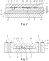
- the electrical modules 2 of the Figure 1 can in embodiments according to Figure 2 be trained.
- the electrical module 2 then has a top 21 and a bottom 22. It comprises a ceramic circuit carrier 260, an electrical component 24 and electrical contacts 31, 32, 33, which are arranged on the top 21 of the module 2.
- the ceramic circuit carrier 260 comprises an insulating ceramic layer 26, a metallization layer 23 arranged on the top of the ceramic layer 26 and a further metallization layer 27 arranged on the underside of the ceramic layer 26.
- the ceramic layer 26 consists, for example, of aluminum nitride (AIN) or silicon nitride (Si 3 N 4 ).
- the metallization layers 23, 27 consist, for example, of copper, aluminum, silver or tungsten.
- the electrical component 24 is arranged on the metallization layer 23 via a solder layer (not shown separately).
- the component 24 has a bottom 241, with which it is arranged on the metallization layer 23, and a top 242.
- the top 242 and the bottom 241 can be metallized, for example copper-plated.
- the electrical component 24 is, for example, a power semiconductor that is designed as a chip.
- the ceramic circuit carrier 260 and the electrical component 24 are arranged in a substrate 28, which defines the external dimensions of the electrical module 2.
- the substrate 28 is a casting compound in which the ceramic circuit carrier 260 and the electrical component 24 are embedded.
- the substrate 28 is a circuit board, in which case the ceramic circuit carrier 260 and the electrical component 24 have been embedded in a circuit board in a circuit board embedding process.
- the substrate 28 includes a top side, which also forms the top side 21 of the module 2.
- the underside of the substrate 28 runs flush with the lower metallization layer 27, which forms the underside 22 of the module 2.
- the ceramic circuit carrier 260 is connected to the lower metallization layer 27 via a heat-conducting material 6 with a heat sink 3. Heat loss from the electrical component 24 is dissipated via the heat sink 3.
- the electrical contacts 31, 32, 33 on the top 21 of the module are provided by solder pads.
- the solder pads 31, 32, 33 are electrically connected to the solder pads 41, 42, 43 of the circuit board 1 via solder connections.
- a drain connection is provided via the solder pad 31 and a source connection and a gate connection of the electrical component 24 are provided via the solder pads 32, 33.
- Through-holes 5 extend from the solder pad 31 and extend to the upper metallization layer 23 of the ceramic circuit carrier 260. Through-holes 50 continue from the solder pads 32, 23, which extend to the top 242 of the electrical component 24.
- the Figure 4 illustrates possible problems that arise when producing a circuit board assembly according to the Figure 1 can arise. This is how it shows Figure 4 two electrical modules 2 (each with a ceramic circuit carrier 260, an electrical component 24 and a spacer 29 in a similar structure to that in relation to Figure 2 explained), which are slightly tilted after soldering onto the circuit board 1 (for example by ⁇ 50 ⁇ m). The tilting can lead to the potting material 7 also covering the underside of the electrical modules 2 in the areas K. However, this should be avoided because this would worsen the thermal transition between the electrical module 2 and the heat sink 3.
- the Figures 5-7 explain a method for producing a circuit board arrangement according to Figure 1 , whereby it is ensured that even if the electrical modules 2 are tilted on the underside of the circuit board 1, the casting compound 7 does not cover the underside 22 of the electrical module.
- a casting compound is provided by means of transfer molding in a tool 110.
- This includes a mold cavity 140 into which a circuit board with electrical modules 2 arranged on it can be inserted.
- a molding compound 70 can be pressed into the mold cavity 140 using channels 120 and a press 130.
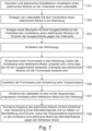
- step 701 at least one electrical module or several electrical modules 2 are arranged on the underside of a circuit board. This is done via a soldering process. Subsequently, in step 702, the circuit board with the electrical modules 2 is inserted into the tool 110, namely in its mold cavity 140.
- the underside 22 of the electrical modules is shown in the illustration Figure 5 directed upwards. For example, 4 ⁇ 5 electrical modules are arranged on the circuit board per panel and inserted into the tool 110.
- a stamp with a compensating film is then placed on the underside 22 of the electrical modules 2 and the compensating film is pressed against the respective underside 22 via the stamp.
- the stamp with the compensation film (not shown separately) is placed from above onto the underside 22 of the respective module 2.
- the compensation film is, for example, a Teflon film.
- the tool 110 is then closed in step 704.
- a molding compound is now injected under pressure into the tool 110 via the channels 120 and left in the tool for a certain time, step 705.
- the volume to be encapsulated is precisely defined by the tool 110 and its mold cavity 140.
- the electrical modules 2 are overmolded without the underside, which is each covered with a compensating film, being covered with the molding compound.
- the compensation film prevents this even if the modules 2 are tilted on the circuit board.
- the residence time of the molding compound in the tool 110 vulcanization or hardening of the molding compound occurs, resulting in the casting compound, step 706.
- the residence time depends on various factors such as the type of resin, any fillers used, processing pressure and processing temperature.
- step 708 the electrical modules 2 are thermally coupled to a heat sink. This is done using a thermally conductive material and means for providing pressure, for example according to the design of the figure 1 .
- the potting material presses the heat-conducting material against the heat sink adjacent to the electrical modules 2.
- the result of using a stamp with a compensation film illustrates this Figure 6 , which represents a single electrical module 2, which is embedded in a casting compound 7.
- the electrical module is, for example, according to the Figure 2 formed and comprises a ceramic circuit carrier with a metallization layer 27, which forms the underside 22 of the electrical module 2.
- a metallization layer 27 At the edges of the metallization layer 27 there is a small vertical offset V1, V2 relative to the surface of the potting material 7, which is, for example, in the range between 0.01 mm and 0.1 mm.
- the underside 22 of the electrical module 2 is free of potting material 7. The offset is caused by the compensating film, which presses against the underside 22 during transfer molding.
Landscapes
- Engineering & Computer Science (AREA)
- Microelectronics & Electronic Packaging (AREA)
- Manufacturing & Machinery (AREA)
- Cooling Or The Like Of Semiconductors Or Solid State Devices (AREA)
Abstract
Description
- Die Erfindung betrifft eine Leiterplattenanordnung gemäß dem Oberbegriff des Patentanspruchs 1 und ein Verfahren zur Herstellung einer solchen Leiterplattenanordnung.
- Es ist bekannt, leiterplattenbasierte Leistungselektronikbaugruppen zur Kühlung an einen Kühlkörper mittels Schraubverbindungen anzupressen, wobei die zu kühlenden Bauteile typischerweise als oberflächenmontierte (SMD-) Bauteile (SMD = "Surface-mounted device") oder in Durchsteckmontage (THT = "Through-Hole-Technology") ausgeführt sind und auf der Unterseite der Leiterplatte sitzen. Die zu kühlenden Bauteile umfassen ein eingebettetes Halbleiterbauelement und werden auch als Prepackage-Module oder - in der vorliegend verwendeten Terminologie - als elektrische Module bezeichnet.
- Je nach Leistungsklasse werden eine hohe Anzahl an zu kühlenden Prepackage-Modulen auf der Unterseite der Leiterplatte angeordnet und zur Kühlung an einen Kühlkörper gepresst. Dabei gilt, dass jeder Spalt zwischen dem zu kühlenden elektrischen Modul und dem Kühlkörper zu einer Verschlechterung der thermischen Anbindung des elektrischen Moduls an den Kühlkörper führt. Ein Spalt zwischen einem zu kühlenden Modul und dem Kühlkörper sollte daher minimiert werden. Bei mehreren elektrischen Modulen, die gekühlt werden müssen, können Spalte mit unterschiedlichen Spaltmaßen zum Kühlkörper vorliegen, die auszugleichen sind. Weitere Toleranzen in den Spaltmaßen ergeben sich aus einer Dickentoleranz der Leiterplatte, lokalen thermischen Durchbiegungen der Leiterplatte und Unebenheiten in der Kühlkörperoberfläche.
- Zum Ausgleich dieser Höhentoleranzen ist es bekannt, Wärmeleitmaterialien einzusetzen. In der Leistungselektronik kommen Pastensysteme oder Folien zum Einsatz, die auf die Kühlfläche appliziert werden und minimale Spalte und Rauheiten bis zu 100 µm ausgleichen. Allerdings liegt ein effektiver Wärmetransport in den Kühlkörper nur im Bereich der elektrischen Module vor, da diese gegen den Kühlkörper gepresst werden und der thermische Widerstand sich bei erhöhtem mechanischen Druck verringert.
- Der vorliegenden Erfindung liegt die Aufgabe zu Grunde, eine Leiterplattenanordnung bereitzustellen, die eine verbesserte thermische Anbindung eines elektrischen Moduls an einen Kühlkörper bereitstellt, sowie ein Verfahren zur Herstellung einer solchen Leiterplattenanordnung anzugeben.
- Diese Aufgabe wird durch eine Leiterplattenanordnung mit den Merkmalen des Anspruchs 1 und ein Verfahren mit den Merkmalen des Anspruchs 17 gelöst. Ausgestaltungen der Erfindung sind in den abhängigen Ansprüchen angegeben.
- Danach betrachtet die Erfindung in einem ersten Erfindungsaspekt eine Leiterplattenanordnung, die eine Leiterplatte mit einer Oberseite und einer Unterseite, mindestens ein auf der Unterseite der Leiterplatte angeordnetes elektrisches Modul, einen Kühlkörper, Mittel zur Bereitstellung eines Drucks, mit dem das elektrische Modul mit seiner Unterseite gegen den Kühlkörper gedrückt wird, und ein Wärmeleitmaterial aufweist, wobei das Wärmeleitmaterial zwischen der Unterseite des elektrischen Moduls und dem Kühlkörper angeordnet ist.
- Es ist vorgesehen, dass das mindestens eine elektrische Modul in ein Vergussmaterial eingebettet ist, das mit der Unterseite des elektrischen Moduls abschließt, ohne die Unterseite zu bedecken, wobei das Vergussmaterial dazu vorgesehen und ausgebildet ist, angrenzend an das mindestens eine elektrische Modul das Wärmeleitmaterial gegen den Kühlkörper zu drücken.
- Die erfindungsgemäße Lösung beruht auf dem Gedanken, die thermische Ankopplung eines elektrischen Moduls an einen Kühlkörper zu verbessern, indem ein Vergussmaterial, in das das elektrische Modul eingegossen ist, die Wärmeleitfolie seitlich des elektrischen Moduls zusätzlich gegen den Kühlkörper drückt, so dass der thermische Übergang zum Kühlkörper auf einer vergrößerten Kühlkörperoberfläche erfolgt.
- Der erfindungsgemäßen Lösung liegt dabei die Erkenntnis zugrunde, dass der thermische Übergang zum Kühlkörper stark vom Anpressdruck an den Kühlkörper abhängt. In herkömmlichen Leiterplattenanordnungen ist der Anpressdruck nur im Bereich der zu kühlenden elektrischen Module hoch, die gegen den Kühlkörper gepresst werden. Neben den elektrischen Modulen liegt das Wärmeleitmaterial dagegen ohne einen Anpressdruck lediglich auf der Kühlkörperoberfläche auf, so dass der Wärmetransport in den Kühlkörper in diesen Bereichen gering ist. Durch Einbetten des elektrischen Moduls bzw. einer Mehrzahl elektrischer Module in ein Vergussmaterial kann auch neben dem elektrischen Modul und zwischen den einzelnen elektrischen Modulen das Wärmeleitmaterial gegen die Kühlkörperoberfläche gepresst werden. Auf diese Weise wird der thermische Übergang zum Kühlkörper insgesamt verbessert.
- Die erfindungsgemäße Lösung erreicht somit eine Verbesserung der Wärmeverteilung über die Oberfläche des Kühlkörpers und damit eine verbesserte Kühlung der elektrischen Module. Dies wiederum erlaubt es, kleinere Kühlsysteme einzusetzen.
- Es wird darauf hingewiesen, dass im Sinne der vorliegenden Erfindung stets diejenige Seite der Leiterplatte, an der ein zu kühlendes elektrisches Modul angeordnet ist, als Unterseite der Leiterplatte bezeichnet wird, unabhängig von der tatsächlichen Orientierung der Leiterplatte und des elektrischen Moduls im Raum.
- Sofern die Leiterplattenanordnung mehrere elektrische Module aufweist, kann vorgesehen sein, dass diese gemeinsam in ein Vergussmaterial eingebettet sind, wobei das Vergussmaterial im Bereich zwischen den elektrischen Modulen das Wärmeleitmaterial gegen den Kühlkörper drückt.
- Das Vergussmaterial erstreckt sich in Ausgestaltungen der Erfindung zumindest abschnittsweise bis an die Unterseite der Leiterplatte, so dass der offene Raum zwischen dem Wärmeleitmaterial und der Unterseite der Leiterplatte vollständig oder zumindest teilweise mit dem Vergussmaterial gefüllt ist. Hierdurch wird eine verbesserte Kühlung aller Bauteile der Leiterplatte durch eine vollflächige Anbindung der Leiterplatte an den Kühlkörper erreicht.
- Darüber hinaus erlaubt diese Ausgestaltung eine partielle elektrische Isolation von kritischen Bereichen auf der Unterseite der Leiterplatte bzw. im Bereich zwischen dem elektrischen Modul und der Leiterplatte. In diesem Zusammenhang ist zu beachten, dass die Anordnung der elektrischen Module an der Leiterplatte bzw. an einer Trägerplatine über einen Lötprozess erfolgt, bei dem einander zugeordnete Lotpads auf dem elektrischen Modul und auf der Leiterplatte über eine Lotschicht miteinander verbunden werden. Dabei entsteht prinzipbedingt ein Luftspalt zwischen dem elektrischen Modul und der Leiterplatte. Dieser Luftspalt wird herkömmlich in einem Underfill-Prozess mit einem Isolationsmaterial vergossen, das unter anderem vor Teilentladungen schützt und die Einhaltung von Luft- und Kriechstrecken ermöglicht. Fertigungsseitig ist die Applikation eines Underfill-Materials allerdings herausfordernd. Das Material wird neben dem elektrischen Modul appliziert und kriecht dann aufgrund der Kapillarwirkung in den Spalt hinein. Hierbei ist die Qualität der Underfill-Schicht im Hinblick auf eine erforderliche Blasenfreiheit von zahlreichen Faktoren abhängig, wie der Sauberkeit des Spalts, der Spalthöhe, der Spaltgeometrie und der verwendeten Oberflächen.
- Die erfindungsgemäße Lösung erlaubt es, einen Underfill-Prozess zu vermeiden und den Spalt zwischen der Oberseite des elektrischen Moduls und der Unterseite der Leiterplatte stattdessen durch das Vergussmaterial zu füllen. So sieht eine Ausgestaltung der Erfindung vor, das elektrische Modul an seiner Oberseite ausgebildete elektrische Lotpads aufweist, die jeweils über eine Lotschicht mit einem zugeordneten elektrischen Lotpad der Leiterplatte in Kontakt stehen, wobei das Vergussmaterial sich angrenzend an die Lotpads auch im Spalt zwischen der Unterseite der Leiterplatte und der Oberseite des elektrischen Moduls erstreckt. Ein Underfill-Material wird somit durch das Vergussmaterial ersetzt. Hierdurch wird das Risiko einer Blasenbildung im Spalt zwischen dem elektrischen Modul und der Leiterplatte verringert, da das Vergussmaterial jeweils in Ausgestaltungen der Erfindung deutlich spaltgängiger ist und zudem mit hohem Druck eingespritzt werden kann, beispielsweise durch Spritzpressen, wie noch ausgeführt wird.
- Eine weitere Ausgestaltung sieht vor, dass das Vergussmaterial des Weiteren solche Bereiche an der Unterseite der Leiterplatte umgibt und elektrisch isoliert, in denen die Leiterplatte Durchkontaktierungen ausbildet. Hierzu wird zum Hintergrund angemerkt, dass die elektrischen Kontakte auf der Leiterplatte typischerweise über Durchkontaktierungen bzw. Vias in der Leiterplatte mit Spannung beaufschlagt werden. Mit solchen Durchkontaktierungen versehene Kontaktflächen der Leiterplatte sind elektrisch zu isolieren. Bei Verwendung eines Underfill-Materials kann dieses aufgrund seiner Vernetzungseigenschaften nicht exakt auf die Leiterplatte und damit auf die zu isolierenden Flächen aufgetragen werden. Dies führt dazu, dass zum Beispiel mittels eines sogenannten "Dam & Fill"-Prozesses weitere Prozessschritte mit einem zusätzlichen Material auszuführen sind, um die Durchkontaktierungen zu isolieren, wobei das zusätzliche Material eine Grenzschicht zum Underfill-Material bildet.
- Die erfindungsgemäße Lösung vermeidet diese Probleme, indem das Vergussmaterial zusätzlich zur Isolation solcher Bereiche an der Unterseite der Leiterplatte dient, in denen die Leiterplatte Durchkontaktierungen ausbildet. Das Vergussmaterial wird somit zur partiellen Isolation von kritischen Bereichen auf der Leiterplatte eingesetzt.
- Eine Ausgestaltung der Erfindung sieht vor, dass das Vergussmaterial eine Härte aufweist, die größer ist als die Härte des Wärmeleitmaterials, so dass es das Wärmeleitmaterial effektiv gegen den Kühlkörper pressen kann. Dabei kann vorgesehen sein, dass das Vergussmaterial als Hartverguss ausgebildet ist. Ausführungsvarianten sehen vor, dass das Vergussmaterial eine Shore-D Härte von größer als 10 aufweist.
- Es handelt sich bei dem Vergussmaterial in Ausführungsbeispielen um einen duroplastischen Kunststoff. Beispielsweise handelt es sich bei dem Vergussmaterial um ein Epoxidharz. Ein Zweikomponenten-Epoxid besteht aus einem Polymerharz und einem Härter, die chemisch miteinander reagieren. Eine Epoxid-Vergussmasse zeichnet sich durch eine hohe Steifigkeit und Zugfestigkeit, eine hohe Temperaturbeständigkeit und eine geringe Schrumpfung aus. Auch besitzt sie eine hohe elektrische Durchschlagsfestigkeit.
- Eine weitere Ausgestaltung der Erfindung sieht vor, dass das mindestens eine elektrische Modul durch Spritzpressen oder Spritzgießen in das Vergussmaterial eingebettet worden ist. Diese Verfahren erlauben es, das elektrische Modul unter Druck in definierter Weise zu umspritzen, wobei das zu umspritzende Volumen exakt definiert werden kann. Dabei können auch bestimmte Bereiche der Leiterplattenanordnung mit Vergussmaterial befüllt und partiell isoliert werden, wie beispielsweise der Spalt zwischen dem elektrischen Modul und der Leiterplatte sowie Via-Bereiche an der Leiterplatte.
- Eine weitere Ausgestaltung sieht vor, dass das Wärmeleitmaterial eine anisotrope Wärmeleitfolie umfasst, die in der Ebene eine erhöhte Wärmeleitfähigkeit beispielsweise im Bereich zwischen als 200 W/mK und 1000 W/mK aufweist. Die Wärmeleitfolie ist dabei beispielsweise eine Graphitfolie. Die Verwendung einer anisotropen Wärmeleitfolie ermöglicht es, die lokal in den elektrischen Modulen entstehende Wärme über die Ebene der Wärmeleitfolie zu spreizen. Die in der Ebene gespreizte Wärme kann dabei effektiv in den Kühlkörper abgeleitet werden, da das Wärmeleitmaterial durch das Vergussmaterial auch angrenzend an die elektrischen Module an den Kühlkörper gepresst wird, so dass ein effektiver thermischer Übergang zum Kühlkörper auf der gesamten Kühlkörperoberfläche vorliegt.
- Die Mittel zur Bereitstellung eines Drucks, mit dem das elektrische Modul mit seiner Unterseite gegen den Kühlkörper gedrückt wird, umfassen beispielsweise Schrauben, die sich von der Oberseite der Leiterplatte in den Kühlkörper erstrecken und in den Kühlkörper eingeschraubt sind. Sie können zusätzlich oder alternativ weitere Mittel enthalten, beispielsweise einen Niederhalter, der von oben gegen die Leiterplatte drückt.
- Das elektrische Modul ist in Ausführungsbeispielen derart aufgebaut, dass es umfasst:
- einen keramischen Schaltungsträger, der eine isolierende Keramikschicht und eine auf der Oberseite der Keramikschicht angeordnete Metallisierungsschicht aufweist, und
- ein elektrisches Bauelement, das auf der Oberseite der Metallisierungsschicht angeordnet und elektrisch mit dieser verbunden ist,
- wobei die Keramikschicht oder eine auf der Unterseite der Keramikschicht ausgebildete zweite Metallisierungsschicht über das Wärmeleitmaterial mit dem Kühlkörper verbunden ist.
- Derartige keramische Schaltungsträger dienen der elektrischen Isolation des mit dem keramischen Schaltungsträger verbundenen elektrischen Bauelements zum Kühlkörper und gleichzeitig der thermischen Anbindung an den Kühlkörper.
- Bei dem in das elektrische Modul integrierten elektrischen Bauelement kann es sich um ein Halbleiterbauelement, insbesondere einen Leistungshalbleiter wie z.B. einen Leistungs-MOSFET oder ein IGBT-Bauelement handeln. Es handelt sich beispielsweise um einen Leistungshalbleiter eines Wechselrichters oder allgemein eines Stromrichters, der für den Betrieb eines Elektromotors vorgesehen ist.
- Weiter kann vorgesehen sein, dass elektrische Kontakte des Moduls mindestens eine erste Durchkontaktierung umfassen, die sich von einem Lotpad an der Oberseite bis zu der ersten Metallisierungsschicht erstreckt, sowie zweite und dritte Durchkontaktierungen umfassen, die sich von anderen Lotpads an der Oberseite zu entsprechenden Kontakten an der Oberseite des elektrischen Bauelements erstrecken. Hierdurch wird eine Kontaktierung des elektrischen Bauelements über an der Oberseite des elektrischen Moduls angeordnete Kontakte ermöglicht.
- Eine weitere Ausgestaltung sieht vor, dass das mindestens eine elektrische Modul in einer Kavität des Kühlkörpers angeordnet ist.
- In einem weiteren Erfindungsaspekt betrifft die vorliegende Erfindung auch ein Verfahren zur Herstellung einer Leiterplattenanordnung. Das Verfahren umfasst die Schritte:
- Anordnen und elektrisches Kontaktieren mindestens eines elektrischen Moduls an der Unterseite einer Leiterplatte,
- Einlegen der Leiterplatte mit dem mindestens einen elektrischen Modul in ein Werkzeug,
- Anlegen eines Stempels mit einer Ausgleichsfolie an die Unterseite des mindestens einen elektrischen Moduls und Drücken der Ausgleichsfolie gegen die Unterseite,
- Schließen des Werkzeugs,
- Einspritzen einer Formmasse in das Werkzeug, wobei das mindestens eine elektrische Modul umspritzt wird, ohne dass die mit der Ausgleichsfolie bedeckte Unterseite des elektrischen Moduls mit der Formmasse bedeckt wird,
- Aushärten der Formmasse unter Entstehung einer Vergussmasse,
- Entnahme der Leiterplatte mit dem mit der Vergussmasse umgossenen mindestens einen elektrischen Modul aus dem Werkzeug, und
- thermisches Koppeln des mindestens einen elektrischen Moduls mit einem Kühlkörper unter Verwendung eines Wärmeleitmaterials und von Mitteln zur Bereitstellung eines Drucks, wobei das Vergussmaterial angrenzend an das mindestens eine elektrische Modul das Wärmeleitmaterial gegen den Kühlkörper drückt.
- Dieser Erfindungsaspekt stellt ein robustes und definiertes Verfahren zur Isolation und Umspritzung von elektrischen Modulen und anderen Leiterplattenbereichen bereit.
- Das Einspritzen einer Formmasse in das Werkzeug erfolgt dabei beispielsweise durch Spritzpressen oder Spritzgießen.
- Eine Ausgestaltung sieht vor, dass beim Einspritzen der Formmasse in das Werkzeug das mindestens eine elektrische Modul dahingehend umspritzt wird, dass die Formmasse auch einen Spalt zwischen der Unterseite der Leiterplatte und der Oberseite des elektrischen Moduls schließt (bis auf jene Bereiche, in denen wie erläutert elektrische Lotpads und Lotschichten ausgebildet sind).
- Weiter kann vorgesehen sein, dass beim Einspritzen der Formmasse in das Werkzeug das mindestens eine elektrische Modul dahingehend umspritzt wird, dass die Formmasse auch solche Bereiche an der Unterseite der Leiterplatte umgibt und elektrisch isoliert, in denen die Leiterplatte Durchkontaktierungen ausbildet.
- Weitere Ausführungsvarianten sehen vor, dass das Verfahren im Nutzen eingesetzt wird, wobei eine Mehrzahl von elektrischen Modulen im Werkzeug gleichzeitig umspritzt wird.
- Die Erfindung wird nachfolgend unter Bezugnahme auf die Figuren der Zeichnung anhand mehrerer Ausführungsbeispiele näher erläutert. Es zeigen:
- Figur 1
- schematisch ein Ausführungsbeispiel einer Leiterplattenanordnung, die ein an einer Leiterplatte angeordnetes elektrisches Modul umfasst, wobei das elektrische Modul in ein Vergussmaterial eingebettet ist, das ein Wärmeleitmaterial gegen einen Kühlkörper drückt;
- Figur 1a
- einen Ausschnitt der Leiterplattenanordnung der
Figur 1 ; - Figur 2
- eine Leiterplattenanordnung gemäß der
Figur 1 , wobei zusätzliche Details im Hinblick auf das elektrische Modul dargestellt sind; - Figur 3
- ein Beispiel einer nicht erfindungsgemäßen Leiterplattenanordnung, die ein an einer Leiterplatte angeordnetes elektrisches Modul umfasst;
- Figur 4
- schematisch die Einbettung zweier elektrischer Module in ein Vergussmaterial in einer nicht erfindungsgemäßen Weise, bei der die Unterseite des elektrischen Moduls mit dem Vergussmaterial bedeckt ist;
- Figur 5
- ein Werkzeug zur Herstellung einer Leiterplattenanordnung gemäß der
Figur 1 ; - Figur 6
- ein elektrisches Modul einer Leiterplattenanordnung gemäß der
Figur 1 , wobei die Unterseite des elektrischen Moduls an ihren Rändern einen vertikalen Versatz zum Vergussmaterial aufweist, in das das elektrische Modul eingebettet ist; und - Figur 7
- ein Ablaufdiagramm eines Verfahrens zur Herstellung einer Leiterplattenanordnung gemäß der
Figur 1 . - Zum besseren Verständnis des Hintergrunds der vorliegenden Erfindung wird anhand der
Figur 3 zunächst eine nicht erfindungsgemäße Leiterplattenanordnung beschrieben. - Die
Figur 3 zeigt eine Leiterplattenanordnung, die eine Leiterplatte 1 und einen Kühlkörper 3 umfasst. Die Leiterplatte 1 besteht aus einer Vielzahl von Leiterplattenlagen (nicht gesondert dargestellt), die übereinander angeordnet sind. Sie weist eine Oberseite 11 und eine Unterseite 12 auf. - Auf der Unterseite 12 der Leiterplatte 1 sind elektrische Module 2 angeordnet. Die Verbindung mit der Leiterplatte 1 erfolgt beispielsweise über eine Oberflächenmontage. Dies ist jedoch lediglich beispielhaft zu verstehen. Zusätzlich können auch an der Oberseite 11 der Leiterplatte 1 elektrische Bauteile angeordnet sein. Von Interesse im vorliegenden Kontext sind die an der Unterseite 12 angeordneten elektrischen Module 2, bei denen es sich um aktive Bauteile handelt (beispielsweise Module der Leistungselektronik), die einer Kühlung durch einen Kühlkörper 3 bedürfen. Hierzu weist der Kühlkörper 3 eine Aussparung 30 auf, in die die zu kühlenden Module 2 hineinragen, wobei die zu kühlenden Module 2 an ihrer Unterseite in thermischen Kontakt mit dem Kühlkörper 3 gelangen.
- Hierbei ist es nachteilig, wenn ein Spalt zwischen dem jeweiligen Modul 2 und dem Kühlkörper 3 vorhanden ist, da ein solcher Spalt die thermische Anbindung an den Kühlkörper 3 verschlechtert. Zur Verbesserung der thermischen Anbindung ist zwischen den zu kühlenden Modulen 2 und dem Kühlkörper 3 ein Wärmeleitmaterial 6 angeordnet.
- Die Leiterplatte 1 ist über Metallschrauben 5 mit dem Kühlkörper 3 verschraubt. Die Metallschrauben 3 sind in Durchgangsbohrungen 15 eingeschraubt, die sich von der Leiterplatte 1 in den Kühlkörper 3 erstrecken. Die Metallschrauben 3 liegen über eine Unterlegscheibe 51 und eine Metallisierung 52 auf der Oberseite 11 der Leiterplatte 1 auf. Sie stellen eine Druckkraft bereit, mit der die Leiterplatte 1 gegen den Kühlkörper 3 gepresst wird. Insbesondere stellen Sie dabei die Druckkraft bereit, mit der die an der Unterseite 12 der Leiterplatte 1 angeordneten zu kühlenden elektrischen Module 2 über das Wärmeleitmaterial 6 an die Oberfläche des Kühlkörpers 3 zur Bereitstellung eines guten thermischen Übergangs angepresst werden.
- Der Kühlkörper 3 kann zahlreiche Ausgestaltungen aufweisen. Er besteht beispielsweise aus einem Metall wie zum Beispiel Aluminium oder einer Aluminiumlegierung und weist nicht gesondert dargestellte Kühlflächen auf. Es handelt sich bei dem Kühlkörper 3 beispielsweise um einen aktiven Kühlkörper, der durch einen Lüfter (nicht dargestellt) oder mittels einer Flüssigkeitskühlung (nicht dargestellt) aktiv gekühlt wird. Alternativ ist der Kühlkörper 3 als passiver Kühlkörper ausgebildet.
- In alternativen Ausgestaltungen (nicht dargestellt) kann vorgesehen sein, dass zur Verbesserung des thermischen Kontaktes zwischen dem zu kühlenden Modul 2 und dem Kühlkörper 3 zusätzlich ein Niederhalter eingesetzt wird, der die Leiterplatte gegen den Kühlkörper drücken.
- Das Wärmeleitmaterial 6 wird in den Bereichen A unterhalb der elektrischen Modul 2 aufgrund der durch die Schrauben 5 bereitgestellten Druckkraft mit hohem mechanischen Druck gegen den Kühlkörper 3 gedrückt. In Bereichen B zwischen den einzelnen elektrischen Modulen 2 bzw. angrenzend an das jeweilige elektrische Modul 2 liegt das Wärmeleitmaterial 2 jedoch lediglich auf. Dies ist in der
Figur 3 nicht maßstabsgerecht durch eine Verwölbung des Wärmeleitmaterials 2 angedeutet. Dementsprechend liegt kein oder ein nur geringer mechanischer Druck auf das Wärmeleitmaterial 2 angrenzend an die elektrischen Module 2 vor. Somit besteht in diesen Bereichen auch ein lediglich reduzierter Wärmetransport aus dem Wärmeleitmaterial 2 in den Kühlkörper 3. - Die
Figur 1 zeigt ein Ausführungsbeispiel einer Leiterplattenanordnung. Der grundlegende Aufbau ist dabei der gleiche wie in Bezug auf dieFigur 3 erläutert, so dass auf die Erläuterungen zurFigur 3 ergänzend Bezug genommen wird. Gemäß derFigur 1 ist vorgesehen, dass die dargestellten elektrischen Module 2 in ein Vergussmaterial 7 eingebettet sind. Das Vergussmaterial 7 schließt dabei mit der Unterseite des elektrischen Moduls ab, ohne die Unterseite zu bedecken. Das Vergussmaterial 7 bewirkt, dass das Wärmeleitmaterial 7 auch in Bereichen B, die an die elektrischen Module 2 angrenzen bzw. zwischen den elektrischen Modulen 2 liegen, mit einem hohen mechanischen Druck gegen den Kühlkörper 3 gedrückt wird. Ein hoher mechanischer Druck liegt sowohl in den Bereichen A unterhalb der elektrischen Module 2 und in den Bereichen B zwischen bzw. neben den elektrischen Modulen 2 vor. - Dabei ist vorgesehen, dass das Vergussmaterial 7 als Hartverguss ausgebildet ist, der eine größere Härte als das Wärmeleitmaterial aufweist. Es handelt sich bei dem Vergussmaterial 7 beispielsweise um ein Epoxidharz oder um einen anderen Duroplast. Die Einbettung der elektrischen Module 2 in das Vergussmaterial 7 erfolgt beispielsweise durch Spritzpressen oder Spritzgießen, wie in Bezug auf die
Figuren 5 bis 7 erläutert wird. - Das Wärmeleitmaterial 7 wird beispielsweise durch eine Wärmeleitfolie, eine Wärmeleitmatte oder ein Wärmeleitpaste gebildet. Dabei kann vorgesehen sein, dass eine anisotropen Wärmeleitfolie, beispielsweise eine Graphitfolie eingesetzt wird, die in der Ebene eine größere Wärmeleitfähigkeit aufweist als in vertikaler Richtung. Die Verwendung einer anisotropen Wärmeleitfolie ermöglicht, die von dem elektrischen Modul 2 ausgehende Wärme in der Fläche zu spreizen. Durch den erfindungsgemäß hohen Anpressdruck auch in den Bereichen B kann die gespreizte Wärme über die gesamte Kühlkörperoberfläche in den Kühlkörper 3 geleitet werden. Dabei sieht eine Ausführungsvariante vor, dass ein Wärmeleitmaterial mit einer hohen thermischen Leitfähigkeit in der Ebene im Bereich zwischen als 200 W/mK und 1000 W/mK eingesetzt wird.
- Wie im Folgenden anhand der Detailansicht der
Figur 1a erläutert wird, die einen Teilbereich der Leiterplattenanordnung derFigur 1 im Bereich eines elektrischen Moduls 2 zeigt, dient das Vergussmaterial 7 auch dazu, kritische Bereiche zwischen dem elektrischen Modul 2 und der Leiterplatte 1 sowie auf der Leiterplatte 1 elektrisch zu isolieren. - So füllt das Vergussmaterial 7 auch einen Spalt 9, der sich zwischen der Oberseite 21 des elektrischen Moduls 2 und der Unterseite 12 der Leiterplatte 1 erstreckt. In dem Spalt 9 befinden sich ferner elektrische Kontakte 8, über die das elektrische Modul 2 elektrisch und mechanisch mit der Unterseite 12 der Leiterplatte 1 verbunden ist. Wie in Bezug auf die
Figur 2 erläutert wird, umfassen diese elektrischen Kontakte 8 typischerweise jeweils ein Lotpad an der Oberseite des elektrischen Moduls, eine Lotschicht und ein Lotpad an der Unterseite der Leiterplatte. - Das Vergussmaterial 7 erstreckt sich im Spalt 9 in Bereichen 71 angrenzend an die elektrischen Kontakte 8 zwischen der Unterseite 12 der Leiterplatte 1 und der Oberseite 21 des elektrischen Moduls 2. Es ersetzt dabei ein Underfill-Material, das mittels eines Underfill-Prozesses in den Spalt 9 eingebracht werden müsste. Hierdurch wird das Risiko einer Blasenbildung im Spalt 9 zwischen dem elektrischen Modul 2 und der Leiterplatte 1 verringert.
- Des Weiteren umgibt und isoliert das Vergussmaterial 7 auch einen Bereich 72 an der Unterseite 12 der Leiterplatte 1, in dem die Leiterplatte Durchkontaktierungen 85 ausbildet. Dabei zeigen die
Figuren 1, 1a schematisch und beispielhaft lediglich eine solche Durchkontaktierung 85. Die Durchkontaktierungen 85 dienen beispielsweise der Beaufschlagung von Lotpads an der Unterseite der Leiterplatte 1 mit Hochspannung. - Es wird darauf hingewiesen, dass die dargestellte Anzahl von zwei elektrischen Modulen 2 in der
Figur 1 lediglich beispielhaft zu verstehen ist. Insbesondere können zwei oder mehr Reihen von elektrischen Modulen hintereinander (senkrecht zur Zeichenebene) vorgesehen sein. - Es wird weiter darauf hingewiesen, dass sich das Vergussmaterial 7 bis an der Unterseite 12 der Leiterplatte 1 erstreckt, die Aussparung 30 im Kühlkörper 3 somit im Wesentlichen vollständig ausfüllt (abgesehen von möglicherweise randseitigen Bereichen, in denen die Aussparung 30 nicht mit Vergussmaterial ausgefüllt ist). Dies führt dazu, dass auch von anderen, nicht dargestellten elektrischen Komponenten der Leiterplatte ausgehende Wärme über die Leiterplatte 1, das Vergussmaterial 7 und das Wärmeleitmaterial 6 in den Kühlkörper 7 abgeleitet werden kann.
- Die Unterseite 22 des elektrischen Moduls 2 drückt ebenso wie die untere Fläche des Vergussmaterials 7 auf das Wärmeleitmaterial 6.
- Die elektrischen Module 2 der
Figur 1 können in Ausführungsbeispielen gemäß derFigur 2 ausgebildet sein. Das elektrische Modul 2 weist danach eine Oberseite 21 und eine Unterseite 22 auf. Es umfasst einen keramischen Schaltungsträger 260, ein elektrisches Bauelement 24 und elektrische Kontakte 31, 32, 33, die auf der Oberseite 21 des Moduls 2 angeordnet sind. Der keramischen Schaltungsträger 260 umfasst eine isolierende Keramikschicht 26, eine auf der Oberseite der Keramikschicht 26 angeordnete Metallisierungsschicht 23 und eine auf der Unterseite der Keramikschicht 26 angeordnete weitere Metallisierungsschicht 27. Die Keramikschicht 26 besteht beispielsweise aus Aluminiumnitrid (AIN) oder Siliziumnitrid (Si3N4). Die Metallisierungsschichten 23, 27 bestehen beispielsweise aus Kupfer, Aluminium, Silber oder Wolfram. - Auf der Metallisierungsschicht 23 ist über eine Lotschicht (nicht gesondert dargestellt) das elektrisches Bauelement 24 angeordnet. Das Bauelement 24 weist dabei eine Unterseite 241, mit der es auf der Metallisierungsschicht 23 angeordnet ist, und eine Oberseite 242 auf. Die Oberseite 242 und die Unterseite 241 können metallisiert, zum Beispiel verkupfert sein. Bei dem elektrischen Bauelement 24 handelt es sich beispielsweise um einen Leistungshalbleiter, der als Chip ausgebildet ist.
- Der keramischen Schaltungsträger 260 und das elektrische Bauelement 24 sind in einem Substrat 28 angeordnet, das die Außenmaße des elektrischen Moduls 2 definiert. Bei dem Substrat 28 handelt es sich in einer Ausführungsvariante um eine Vergussmasse, in die der keramischen Schaltungsträger 260 und das elektrische Bauelement 24 eingebettet sind. Alternativ handelt es sich bei dem Substrat 28 um eine Leiterplatte, für welchen Fall der keramischen Schaltungsträger 260 und das elektrische Bauelement 24 in einem Leiterplattenembeddingprozess in eine Leiterplatte eingebettet worden sind.
- Das Substrat 28 umfasst eine Oberseite, die auch die Oberseite 21 des Moduls 2 bildet. Die Unterseite des Substrat 28 verläuft bündig mit der unteren Metallisierungsschicht 27, die die Unterseite 22 des Moduls 2 bildet. Der keramische Schaltungsträger 260 ist mit der unteren Metallisierungsschicht 27 über ein Wärmeleitmaterial 6 mit einem Kühlkörper 3 verbunden. Über den Kühlkörper 3 wird Verlustwärme des elektrischen Bauelements 24 abgeführt.
- Die elektrische Kontakte 31, 32, 33 an der Oberseite 21 des Moduls werden durch Lotpads bereitgestellt. Die Lotpads 31, 32, 33 sind über Lotverbindungen mit den Lotpads 41, 42, 43 der Leiterplatte 1 elektrisch verbunden. Dabei werden über das Lotpad 31 beispielsweise ein Drain-Anschluss und über die Lotpads 32, 33 ein Source-Anschluss und ein Gate-Anschluss des elektrischen Bauelements 24 bereitgestellt.
- Von dem Lotpad 31 gehen Durchkontaktierungen 5 aus, die sich zu der oberen Metallisierungsschicht 23 des keramischen Schaltungsträgers 260 erstrecken. Weiter gehen von den Lotpads 32, 23 Durchkontaktierungen 50 aus, die sich zu der Oberseite 242 des elektrischen Bauelements 24 erstrecken.
- Die
Figur 4 verdeutlicht mögliche Probleme, die bei der Herstellung einer Leiterplattenanordnung gemäß derFigur 1 entstehen können. So zeigt dieFigur 4 zwei elektrische Module 2 (jeweils mit einem keramischen Schaltungsträger 260, einem elektrischen Bauelement 24 und einem Abstandshalter 29 in ähnlichem Aufbau wie in Bezug auf dieFigur 2 erläutert), die nach dem Auflöten auf die Leiterplatte 1 leicht verkippt sind (beispielsweise um ± 50 µm). Die Verkippung kann dazu führen, dass in den Bereichen K das Vergussmaterial 7 auch die Unterseite der elektrischen Module 2 bedeckt. Dies ist allerdings zu vermeiden, weil hierdurch der thermische Übergang zwischen dem elektrischen Modul 2 und dem Kühlkörper 3 verschlechtert würde. - Die
Figuren 5-7 erläutern ein Verfahren zur Herstellung einer Leiterplattenanordnung gemäß derFigur 1 , wobei sichergestellt ist, dass auch bei einer verkippten Anordnung der elektrischen Module 2 an der Unterseite der Leiterplatte 1 die Vergussmasse 7 die Unterseite 22 des elektrischen Moduls nicht bedeckt. - Die Bereitstellung einer Vergussmasse erfolgt mittels Spritzpressen in einem Werkzeug 110. Dieses umfasst ein Formnest 140, in das eine Leiterplatte mit daran angeordneten elektrischen Modulen 2 einlegbar ist. In das Formnest 140 kann mittels Kanälen 120 und eine Presse 130 eine Formmasse 70 eingepresst werden.
- Die
Figur 7 erläuterte das Verfahren. Zunächst werden in Schritt 701 mindestens ein elektrisches Modul bzw. mehrere elektrische Module 2 an der Unterseite einer Leiterplatte angeordnet. Dies erfolgt über einen Lötprozess. Anschließend wird in Schritt 702 die Leiterplatte mit den elektrischen Modulen 2 in das Werkzeug 110 eingelegt, nämlich in dessen Formnest 140. Dabei ist die Unterseite 22 der elektrischen Module in der Darstellung derFigur 5 nach oben gerichtet. Beispielsweise werden pro Nutzen 4 × 5 elektrische Module an der Leiterplatte angeordnet und in das Werkzeug 110 eingelegt. - Gemäß Schritt 703 wird anschließend jeweils ein Stempel mit einer Ausgleichsfolie an die Unterseite 22 der elektrischen Module 2 angelegt und über den Stempel die Ausgleichsfolie gegen die jeweilige Unterseite 22 gedrückt. In der Darstellung der
Figur 5 wird dabei der Stempel mit der Ausgleichsfolie (nicht gesondert dargestellt) von oben auf die Unterseite 22 des jeweiligen Moduls 2 angelegt. Die Ausgleichsfolie ist beispielsweise eine Teflonfolie. Anschließend wird das Werkzeug 110 in Schritt 704 geschlossen. Es wird nun über die Kanäle 120 eine Formmasse unter Druck in das Werkzeug 110 eingespritzt und für eine bestimmte Zeit im Werkzeug belassen, Schritt 705. Dabei wird durch das Werkzeug 110 und dessen Formnest 140 das zu umspritzende Volumen exakt definiert. Die elektrischen Module 2 werden dabei umspritzt, ohne dass die jeweils mit einer Ausgleichsfolie bedeckte Unterseite mit der Formmasse bedeckt wird. Die Ausgleichsfolie verhindert dies selbst dann, wenn die Module 2 verkippt an der Leiterplatte angeordnet sind. - Während der Verweilzeit der Formmasse im Werkzeug 110 kommt es zum Vulkanisieren oder Aushärten der Formmasse, wobei die Vergussmasse entsteht, Schritt 706. Die Verweilzeit ist dabei von verschiedenen Faktoren abhängig wie zum Beispiel Harztyp, ggf. verwendeten Füllstoffen, Verarbeitungsdruck und Verarbeitungstemperatur. Ist die Verweilzeit beendet, wird das Werkzeug 110 geöffnet und wird die Leiterplatte mit den mit der Vergussmasse umgossenen elektrischen Modulen 2 aus dem Werkzeug 110 entnommen, Schritt 707.
- Anschließend werden in Schritt 708 die elektrischen Module 2 mit einem Kühlkörper thermisch gekoppelt. Dies erfolgt unter Verwendung eines Wärmeleitmaterials und Mitteln zur Bereitstellung eines Drucks, entsprechend beispielsweise der Ausgestaltung der
Figur 1 . Dabei drückt das Vergussmaterial angrenzend an die elektrischen Module 2 das Wärmeleitmaterial gegen den Kühlkörper. - Das Ergebnis der Verwendung eines Stempels mit einer Ausgleichsfolie verdeutlicht die
Figur 6 , die ein einzelnes elektrisches Modul 2 darstellt, das in eine Vergussmasse 7 eingebettet ist. Das elektrische Modul ist beispielsweise entsprechend derFigur 2 ausgebildet und umfasst einen keramischen Schaltungsträger mit einer Metallisierungsschicht 27, die die Unterseite 22 des elektrischen Moduls 2 bildet. An den Rändern der Metallisierungsschicht 27 liegt jeweils ein kleiner vertikaler Versatz V1, V2 gegenüber der Oberfläche des Vergussmaterial 7 vor, der beispielsweise im Bereich zwischen 0,01 mm und 0,1 mm liegt. Dabei ist die Unterseite 22 des elektrischen Moduls 2 frei von Vergussmaterial 7. Der Versatz entsteht durch die Ausgleichsfolie, die während des Spritzpressens gegen die Unterseite 22 drückt. - Es versteht sich, dass die Erfindung nicht auf die oben beschriebenen Ausführungsformen beschränkt ist und verschiedene Modifikationen und Verbesserungen vorgenommen werden können, ohne von den hier beschriebenen Konzepten abzuweichen. Weiter wird darauf hingewiesen, dass beliebige der beschriebenen Merkmale separat oder in Kombination mit beliebigen anderen Merkmalen eingesetzt werden können, sofern sie sich nicht gegenseitig ausschließen. Die Offenbarung dehnt sich auf alle Kombinationen und Unterkombinationen eines oder mehrerer Merkmale aus, die hier beschrieben werden und umfasst diese. Sofern Bereiche definiert sind, so umfassen diese sämtliche Werte innerhalb dieser Bereiche sowie sämtliche Teilbereiche, die in einen Bereich fallen.
Claims (15)
- Leiterplattenanordnung, die aufweist:- eine Leiterplatte (1) mit einer Oberseite (11) und einer Unterseite (12),- mindestens ein elektrisches Modul (2) mit einer Oberseite (21) und einer Unterseite (22), das mit seiner Oberseite (21) an der Unterseite (12) der Leiterplatte (1) angeordnet ist,- einen Kühlkörper (3),- Mittel (5) zur Bereitstellung eines Drucks, mit dem das elektrische Modul (2) mit seiner Unterseite (22) gegen den Kühlkörper (3) gedrückt wird, und- ein Wärmeleitmaterial (6), das zwischen der Unterseite (22) des elektrischen Moduls (2) und dem Kühlkörper (3) angeordnet ist,dadurch gekennzeichnet,
dass das mindestens eine elektrische Modul (2) in ein Vergussmaterial (7) eingebettet ist, das mit der Unterseite (22) des elektrischen Moduls (2) abschließt, ohne die Unterseite (22) zu bedecken, wobei das Vergussmaterial (7) dazu vorgesehen und ausgebildet ist, angrenzend an das mindestens eine elektrische Modul (2) das Wärmeleitmaterial (6) gegen den Kühlkörper (3) zu drücken. - Leiterplattenanordnung nach Anspruch 1, dadurch gekennzeichnet, dass die Leiterplattenanordnung mehrere elektrische Module (2) aufweist, die in das Vergussmaterial (7) eingebettet sind, wobei das Vergussmaterial (7) dazu vorgesehen und ausgebildet ist, im Bereich (B) zwischen den elektrischen Modulen (2) das Wärmeleitmaterial (6) gegen den Kühlkörper (3) zu drücken.
- Leiterplattenanordnung nach Anspruch 1 oder 2, dadurch gekennzeichnet, dass das Vergussmaterial (7) sich zumindest abschnittsweise bis an die Unterseite (12) der Leiterplatte (1) erstreckt.
- Leiterplattenanordnung nach einem der vorangehenden Ansprüche, dadurch gekennzeichnet, dass das elektrische Modul (2) an seiner Oberseite (21) ausgebildete elektrische Lotpads (31-33) aufweist, die jeweils über eine Lotschicht mit einem zugeordneten elektrischen Lotpad (41-43) der Leiterplatte (1) in Kontakt stehen, wobei das Vergussmaterial (7) sich angrenzend an die Lotpads (31-33) auch im Spalt (9) zwischen der Unterseite (12) der Leiterplatte (1) und der Oberseite (21) des elektrischen Moduls (2) erstreckt.
- Leiterplattenanordnung nach einem der vorangehenden Ansprüche, dadurch gekennzeichnet, dass das Vergussmaterial (7) solche Bereiche an der Unterseite der Leiterplatte umgibt und elektrisch isoliert, in denen die Leiterplatte (1) Durchkontaktierungen (85) ausbildet.
- Leiterplattenanordnung nach einem der vorangehenden Ansprüche, dadurch gekennzeichnet, dass das Vergussmaterial (7) eine Härte aufweist, die größer ist als die Härte des Wärmeleitmaterials (6), und/oder ein Epoxidharz ist.
- Leiterplattenanordnung nach einem der vorangehenden Ansprüche, dadurch gekennzeichnet, dass das mindestens eine elektrische Modul (2) durch Spritzpressen oder Spritzgießen in das Vergussmaterial (7) eingebettet worden ist.
- Leiterplattenanordnung nach einem der vorangehenden Ansprüche, dadurch gekennzeichnet, dass das mindestens eine elektrische Modul (2) umfasst:- einen keramischen Schaltungsträger (260), der eine isolierende Keramikschicht (26) und eine auf der Oberseite der Keramikschicht (26) angeordnete Metallisierungsschicht (23) aufweist,- ein elektrisches Bauelement (24), das auf der Oberseite der Metallisierungsschicht (23) angeordnet und elektrisch mit dieser verbunden ist,- wobei die Keramikschicht (26) oder eine auf der Unterseite der Keramikschicht (26) ausgebildete zweite Metallisierungsschicht (27) über das Wärmeleitmaterial (6) mit dem Kühlkörper (3) verbunden ist.
- Leiterplattenanordnung nach Anspruch 8, dadurch gekennzeichnet, dass das elektrische Bauelement (24) ein Halbleiterbauelement, insbesondere ein Leistungshalbleiter ist.
- Leiterplattenanordnung nach Anspruch 8 oder 9, dadurch gekennzeichnet, dass elektrische Kontakte des Moduls (2) mindestens eine erste Durchkontaktierung (5) umfassen, die sich von einem Lotpad (31) an der Oberseite (21) bis zu der ersten Metallisierungsschicht (23) erstreckt, sowie zweite und dritte Durchkontaktierungen (50) umfassen, die sich von anderen Lotpads (32, 33) an der Oberseite (21) zu entsprechenden Kontakten an der Oberseite (242) des elektrischen Bauelements (24) erstrecken.
- Leiterplattenanordnung nach einem der vorangehenden Ansprüche, dadurch gekennzeichnet, dass das mindestens eine elektrische Modul (2) in einer Kavität (30) des Kühlkörpers (3) angeordnet ist.
- Verfahren zur Herstellung einer Leiterplattenanordnung, das die Schritte umfasst:- Anordnen (701) und elektrisches Kontaktieren mindestens eines elektrischen Moduls (2) an der Unterseite einer Leiterplatte (1),- Einlegen (702) der Leiterplatte (1) mit dem mindestens einen elektrischen Modul (2) in ein Werkzeug (110),- Anlegen (703) eines Stempels mit einer Ausgleichsfolie an die Unterseite (22) des mindestens einen elektrischen Moduls (2) und Drücken der Ausgleichsfolie gegen die Unterseite,- Schließen (704) des Werkzeugs (110),- Einspritzen (705) einer Formmasse in das Werkzeug (110), wobei das mindestens eine elektrische Modul (2) umspritzt wird, ohne dass die mit der Ausgleichsfolie bedeckte Unterseite (22) des elektrischen Moduls (2) mit der Formmasse bedeckt wird,- Aushärten (706) der Formmasse unter Entstehung einer Vergussmasse (7),- Entnahme (707) der Leiterplatte (1) mit dem mit der Vergussmasse (7) umgossenen mindestens einen elektrischen Modul (2) aus dem Werkzeug (110), und- thermisches (708) Koppeln des mindestens einen elektrischen Moduls (2) mit einem Kühlkörper (3) unter Verwendung eines Wärmeleitmaterials (6) und von Mitteln (5) zur Bereitstellung eines Drucks, wobei das Vergussmaterial (7) angrenzend an das mindestens eine elektrische Modul (2) das Wärmeleitmaterial (6) gegen den Kühlkörper (3) drückt.
- Verfahren nach Anspruch 12, dadurch gekennzeichnet, dass beim Einspritzen (705) der Formmasse in das Werkzeug (110) das mindestens eine elektrische Modul (2) dahingehend umspritzt wird, dass die Formmasse auch einen Spalt (9) zwischen der Unterseite der Leiterplatte (1) und der Oberseite des elektrischen Moduls (2) schließt.
- Verfahren nach Anspruch 12 oder 13, dadurch gekennzeichnet, dass beim Einspritzen (705) der Formmasse in das Werkzeug (110) das mindestens eine elektrische Modul (2) dahingehend umspritzt wird, dass die Formmasse auch solche Bereiche an der Unterseite der Leiterplatte (1) umgibt und elektrisch isoliert, in denen die Leiterplatte Durchkontaktierungen (85) ausbildet.
- Verfahren nach einem der Ansprüche 12 bis 14, dadurch gekennzeichnet, dass in einem Nutzen eine Mehrzahl von elektrischen Modulen (2) im Werkzeug gleichzeitig umspritzt wird.
Applications Claiming Priority (1)
| Application Number | Priority Date | Filing Date | Title |
|---|---|---|---|
| DE102022124513.6A DE102022124513A1 (de) | 2022-09-23 | 2022-09-23 | Leiterplattenanordnung und Verfahren zur Herstellung einer Leiterplattenanordnung |
Publications (2)
| Publication Number | Publication Date |
|---|---|
| EP4343828A1 true EP4343828A1 (de) | 2024-03-27 |
| EP4343828B1 EP4343828B1 (de) | 2025-04-09 |
Family
ID=88098280
Family Applications (1)
| Application Number | Title | Priority Date | Filing Date |
|---|---|---|---|
| EP23198522.7A Active EP4343828B1 (de) | 2022-09-23 | 2023-09-20 | Leiterplattenanordnung und verfahren zur herstellung einer leiterplattenanordnung |
Country Status (3)
| Country | Link |
|---|---|
| US (1) | US20240105548A1 (de) |
| EP (1) | EP4343828B1 (de) |
| DE (1) | DE102022124513A1 (de) |
Families Citing this family (2)
| Publication number | Priority date | Publication date | Assignee | Title |
|---|---|---|---|---|
| DE102023111238A1 (de) * | 2023-05-02 | 2024-11-07 | Schaeffler Technologies AG & Co. KG | Vorrichtung zur Kühlung mindestens eines Leistungshalbleiters eines Schaltungsträgers |
| DE102025101191B3 (de) | 2025-01-14 | 2026-03-26 | Volkswagen Aktiengesellschaft | Vorrichtung für einen Stromwandler, Stromwandler und Fahrzeug |
Citations (3)
| Publication number | Priority date | Publication date | Assignee | Title |
|---|---|---|---|---|
| JP2015211600A (ja) * | 2014-04-29 | 2015-11-24 | 三菱電機株式会社 | 電力変換装置 |
| US20200203301A1 (en) * | 2018-12-24 | 2020-06-25 | Taiwan Semiconductor Manufacturing Co., Ltd. | Electronic assembly, package structure and method of fabricating the same |
| US20210233830A1 (en) * | 2020-01-29 | 2021-07-29 | Mitsubishi Electric Corporation | Semiconductor device |
Family Cites Families (12)
| Publication number | Priority date | Publication date | Assignee | Title |
|---|---|---|---|---|
| US5786635A (en) * | 1996-12-16 | 1998-07-28 | International Business Machines Corporation | Electronic package with compressible heatsink structure |
| US6631078B2 (en) * | 2002-01-10 | 2003-10-07 | International Business Machines Corporation | Electronic package with thermally conductive standoff |
| US6940712B2 (en) * | 2002-07-17 | 2005-09-06 | International Business Machines Corporation | Electronic device substrate assembly with multilayer impermeable barrier and method of making |
| TW592030B (en) * | 2003-04-29 | 2004-06-11 | Quanta Comp Inc | Functional module and manufacturing method thereof |
| DE102004037656B4 (de) * | 2004-08-03 | 2009-06-18 | Infineon Technologies Ag | Elektronikmodul mit optimierter Montagefähigkeit und Bauteilanordnung mit einem Elektronikmodul |
| US7462506B2 (en) * | 2006-06-15 | 2008-12-09 | International Business Machines Corporation | Carbon dioxide gettering method for a chip module assembly |
| US20090129024A1 (en) * | 2007-11-15 | 2009-05-21 | Dennis Mahoney | Inverted through circuit board mounting with heat sink |
| US20090213541A1 (en) * | 2008-02-27 | 2009-08-27 | Matthew Allen Butterbaugh | Cooling Plate Assembly with Fixed and Articulated Interfaces, and Method for Producing Same |
| US9402319B2 (en) * | 2011-05-11 | 2016-07-26 | Vlt, Inc. | Panel-molded electronic assemblies |
| US9385059B2 (en) * | 2013-08-28 | 2016-07-05 | Infineon Technologies Ag | Overmolded substrate-chip arrangement with heat sink |
| DE102019209069A1 (de) * | 2019-06-24 | 2020-12-24 | Siemens Aktiengesellschaft | Befestigung von Leistungshalbleiterbauelementen auf gekrümmten Oberflächen |
| DE102022113642A1 (de) * | 2022-05-31 | 2023-11-30 | Rolls-Royce Deutschland Ltd & Co Kg | Leiterplattenanordnung |
-
2022
- 2022-09-23 DE DE102022124513.6A patent/DE102022124513A1/de active Pending
-
2023
- 2023-09-20 EP EP23198522.7A patent/EP4343828B1/de active Active
- 2023-09-23 US US18/372,085 patent/US20240105548A1/en active Pending
Patent Citations (3)
| Publication number | Priority date | Publication date | Assignee | Title |
|---|---|---|---|---|
| JP2015211600A (ja) * | 2014-04-29 | 2015-11-24 | 三菱電機株式会社 | 電力変換装置 |
| US20200203301A1 (en) * | 2018-12-24 | 2020-06-25 | Taiwan Semiconductor Manufacturing Co., Ltd. | Electronic assembly, package structure and method of fabricating the same |
| US20210233830A1 (en) * | 2020-01-29 | 2021-07-29 | Mitsubishi Electric Corporation | Semiconductor device |
Also Published As
| Publication number | Publication date |
|---|---|
| DE102022124513A1 (de) | 2024-03-28 |
| US20240105548A1 (en) | 2024-03-28 |
| EP4343828B1 (de) | 2025-04-09 |
Similar Documents
| Publication | Publication Date | Title |
|---|---|---|
| EP2422367B1 (de) | Gekapselte schaltungsvorrichtung für substrate mit absorptionsschicht sowie verfahren zu herstellung derselben | |
| DE102013219833B4 (de) | Halbleitermodul mit leiterplatte und vefahren zur hertellung eines halbleitermoduls mit einer leiterplatte | |
| DE102018121403B4 (de) | Verfahren zur Herstellung einer stabilisierten Platine | |
| DE19617055C1 (de) | Halbleiterleistungsmodul hoher Packungsdichte in Mehrschichtbauweise | |
| DE102018207955B4 (de) | Leiterplattenmodul mit integriertem leistungselektronischen Metall-Keramik-Modul sowie Verfahren zu dessen Herstellung | |
| DE10238037B4 (de) | Halbleitereinrichtung mit Gehäuse und Halterung | |
| EP3231261B1 (de) | Leiterplatte mit einem asymmetrischen schichtenaufbau | |
| EP4343828B1 (de) | Leiterplattenanordnung und verfahren zur herstellung einer leiterplattenanordnung | |
| DE102008008141A1 (de) | Leistungshalbleitermodul und Verfahren zu seiner Herstellung | |
| DE19634202C2 (de) | Halbleitervorrichtung | |
| DE102015115132B4 (de) | Halbleitermodul mit integrierter Stift- oder Rippenkühlstruktur und Verfahren zu seiner Herstellung | |
| DE102008039921B4 (de) | Verfahren zur Herstellung eines elektronischen Geräts mit diskretem Bauelement | |
| DE102022113639A1 (de) | Elektrisches Modul | |
| EP0938252A2 (de) | Elektrische Schaltungsanordnung | |
| DE102022113642A1 (de) | Leiterplattenanordnung | |
| WO2020078778A1 (de) | Halbleiterbauelement-anordnung, verfahren zu deren herstellung sowie entwärmungseinrichtung | |
| WO2016146613A1 (de) | Elektronische steuervorrichtung | |
| DE102022119084A1 (de) | Leiterplattenanordnung | |
| WO2018050382A1 (de) | Elektronische baugruppe, insbesondere für ein getriebesteuermodul, und verfahren zum herstellen einer elektronischen baugruppe | |
| DE10125697B4 (de) | Leistungshalbleitermodul und Verfahren zum Herstellen eines Leistungshalbleitermoduls | |
| DE102018204553B4 (de) | Leistungselektronikmodul für Kraftfahrzeuganwendungen | |
| DE102018216597A1 (de) | Leiterplattenvorrichtung, Verfahren zum Herstellen einer Leiterplattenvorrichtung und Getriebesystem für ein Fahrzeug mit einer Leiterplattenvorrichtung | |
| DE102024100581A1 (de) | Halbleitervorrichtung und Verfahren zum Herstellen einer Halbleitervorrichtung | |
| EP4042476B1 (de) | Leistungshalbleiterbauteil sowie verfahren zur herstellung eines leistungshalbleiterbauteils | |
| DE102022113643A1 (de) | Elektrisches Modul |
Legal Events
| Date | Code | Title | Description |
|---|---|---|---|
| PUAI | Public reference made under article 153(3) epc to a published international application that has entered the european phase |
Free format text: ORIGINAL CODE: 0009012 |
|
| STAA | Information on the status of an ep patent application or granted ep patent |
Free format text: STATUS: THE APPLICATION HAS BEEN PUBLISHED |
|
| AK | Designated contracting states |
Kind code of ref document: A1 Designated state(s): AL AT BE BG CH CY CZ DE DK EE ES FI FR GB GR HR HU IE IS IT LI LT LU LV MC ME MK MT NL NO PL PT RO RS SE SI SK SM TR |
|
| STAA | Information on the status of an ep patent application or granted ep patent |
Free format text: STATUS: REQUEST FOR EXAMINATION WAS MADE |
|
| 17P | Request for examination filed |
Effective date: 20240429 |
|
| RBV | Designated contracting states (corrected) |
Designated state(s): AL AT BE BG CH CY CZ DE DK EE ES FI FR GB GR HR HU IE IS IT LI LT LU LV MC ME MK MT NL NO PL PT RO RS SE SI SK SM TR |
|
| RIC1 | Information provided on ipc code assigned before grant |
Ipc: H05K 3/28 20060101ALN20241001BHEP Ipc: H01L 25/11 20060101ALN20241001BHEP Ipc: H01L 23/051 20060101ALN20241001BHEP Ipc: H01L 21/56 20060101ALI20241001BHEP Ipc: H01L 23/40 20060101ALI20241001BHEP Ipc: H01L 23/433 20060101ALI20241001BHEP Ipc: H01L 23/538 20060101ALI20241001BHEP Ipc: H05K 1/02 20060101ALI20241001BHEP Ipc: H01L 25/065 20230101ALI20241001BHEP Ipc: H01L 25/07 20060101ALI20241001BHEP Ipc: H01L 23/373 20060101AFI20241001BHEP |
|
| GRAP | Despatch of communication of intention to grant a patent |
Free format text: ORIGINAL CODE: EPIDOSNIGR1 |
|
| STAA | Information on the status of an ep patent application or granted ep patent |
Free format text: STATUS: GRANT OF PATENT IS INTENDED |
|
| RIC1 | Information provided on ipc code assigned before grant |
Ipc: H05K 3/28 20060101ALN20241014BHEP Ipc: H01L 25/11 20060101ALN20241014BHEP Ipc: H01L 23/051 20060101ALN20241014BHEP Ipc: H01L 21/56 20060101ALI20241014BHEP Ipc: H01L 23/40 20060101ALI20241014BHEP Ipc: H01L 23/433 20060101ALI20241014BHEP Ipc: H01L 23/538 20060101ALI20241014BHEP Ipc: H05K 1/02 20060101ALI20241014BHEP Ipc: H01L 25/065 20230101ALI20241014BHEP Ipc: H01L 25/07 20060101ALI20241014BHEP Ipc: H01L 23/373 20060101AFI20241014BHEP |
|
| RIC1 | Information provided on ipc code assigned before grant |
Ipc: H05K 3/28 20060101ALN20241018BHEP Ipc: H01L 25/11 20060101ALN20241018BHEP Ipc: H01L 23/051 20060101ALN20241018BHEP Ipc: H01L 21/56 20060101ALI20241018BHEP Ipc: H01L 23/40 20060101ALI20241018BHEP Ipc: H01L 23/433 20060101ALI20241018BHEP Ipc: H01L 23/538 20060101ALI20241018BHEP Ipc: H05K 1/02 20060101ALI20241018BHEP Ipc: H01L 25/065 20230101ALI20241018BHEP Ipc: H01L 25/07 20060101ALI20241018BHEP Ipc: H01L 23/373 20060101AFI20241018BHEP |
|
| RIC1 | Information provided on ipc code assigned before grant |
Ipc: H05K 3/28 20060101ALN20241106BHEP Ipc: H01L 25/11 20060101ALN20241106BHEP Ipc: H01L 23/051 20060101ALN20241106BHEP Ipc: H01L 21/56 20060101ALI20241106BHEP Ipc: H01L 23/40 20060101ALI20241106BHEP Ipc: H01L 23/433 20060101ALI20241106BHEP Ipc: H01L 23/538 20060101ALI20241106BHEP Ipc: H05K 1/02 20060101ALI20241106BHEP Ipc: H01L 25/065 20230101ALI20241106BHEP Ipc: H01L 25/07 20060101ALI20241106BHEP Ipc: H01L 23/373 20060101AFI20241106BHEP |
|
| INTG | Intention to grant announced |
Effective date: 20241119 |
|
| GRAS | Grant fee paid |
Free format text: ORIGINAL CODE: EPIDOSNIGR3 |
|
| GRAA | (expected) grant |
Free format text: ORIGINAL CODE: 0009210 |
|
| STAA | Information on the status of an ep patent application or granted ep patent |
Free format text: STATUS: THE PATENT HAS BEEN GRANTED |
|
| P01 | Opt-out of the competence of the unified patent court (upc) registered |
Free format text: CASE NUMBER: APP_8263/2025 Effective date: 20250218 |
|
| AK | Designated contracting states |
Kind code of ref document: B1 Designated state(s): AL AT BE BG CH CY CZ DE DK EE ES FI FR GB GR HR HU IE IS IT LI LT LU LV MC ME MK MT NL NO PL PT RO RS SE SI SK SM TR |
|
| REG | Reference to a national code |
Ref country code: GB Ref legal event code: FG4D Free format text: NOT ENGLISH |
|
| REG | Reference to a national code |
Ref country code: CH Ref legal event code: EP |
|
| REG | Reference to a national code |
Ref country code: DE Ref legal event code: R096 Ref document number: 502023000807 Country of ref document: DE |
|
| REG | Reference to a national code |
Ref country code: IE Ref legal event code: FG4D Free format text: LANGUAGE OF EP DOCUMENT: GERMAN |
|
| REG | Reference to a national code |
Ref country code: NL Ref legal event code: MP Effective date: 20250409 |
|
| PG25 | Lapsed in a contracting state [announced via postgrant information from national office to epo] |
Ref country code: NL Free format text: LAPSE BECAUSE OF FAILURE TO SUBMIT A TRANSLATION OF THE DESCRIPTION OR TO PAY THE FEE WITHIN THE PRESCRIBED TIME-LIMIT Effective date: 20250409 |
|
| PG25 | Lapsed in a contracting state [announced via postgrant information from national office to epo] |
Ref country code: FI Free format text: LAPSE BECAUSE OF FAILURE TO SUBMIT A TRANSLATION OF THE DESCRIPTION OR TO PAY THE FEE WITHIN THE PRESCRIBED TIME-LIMIT Effective date: 20250409 Ref country code: PT Free format text: LAPSE BECAUSE OF FAILURE TO SUBMIT A TRANSLATION OF THE DESCRIPTION OR TO PAY THE FEE WITHIN THE PRESCRIBED TIME-LIMIT Effective date: 20250811 Ref country code: ES Free format text: LAPSE BECAUSE OF FAILURE TO SUBMIT A TRANSLATION OF THE DESCRIPTION OR TO PAY THE FEE WITHIN THE PRESCRIBED TIME-LIMIT Effective date: 20250409 |
|
| PGFP | Annual fee paid to national office [announced via postgrant information from national office to epo] |
Ref country code: DE Payment date: 20250926 Year of fee payment: 3 |
|
| REG | Reference to a national code |
Ref country code: LT Ref legal event code: MG9D |
|
| PG25 | Lapsed in a contracting state [announced via postgrant information from national office to epo] |
Ref country code: NO Free format text: LAPSE BECAUSE OF FAILURE TO SUBMIT A TRANSLATION OF THE DESCRIPTION OR TO PAY THE FEE WITHIN THE PRESCRIBED TIME-LIMIT Effective date: 20250709 Ref country code: GR Free format text: LAPSE BECAUSE OF FAILURE TO SUBMIT A TRANSLATION OF THE DESCRIPTION OR TO PAY THE FEE WITHIN THE PRESCRIBED TIME-LIMIT Effective date: 20250710 |
|
| PG25 | Lapsed in a contracting state [announced via postgrant information from national office to epo] |
Ref country code: PL Free format text: LAPSE BECAUSE OF FAILURE TO SUBMIT A TRANSLATION OF THE DESCRIPTION OR TO PAY THE FEE WITHIN THE PRESCRIBED TIME-LIMIT Effective date: 20250409 |
|
| PG25 | Lapsed in a contracting state [announced via postgrant information from national office to epo] |
Ref country code: BG Free format text: LAPSE BECAUSE OF FAILURE TO SUBMIT A TRANSLATION OF THE DESCRIPTION OR TO PAY THE FEE WITHIN THE PRESCRIBED TIME-LIMIT Effective date: 20250409 |
|
| PG25 | Lapsed in a contracting state [announced via postgrant information from national office to epo] |
Ref country code: HR Free format text: LAPSE BECAUSE OF FAILURE TO SUBMIT A TRANSLATION OF THE DESCRIPTION OR TO PAY THE FEE WITHIN THE PRESCRIBED TIME-LIMIT Effective date: 20250409 |
|
| PGFP | Annual fee paid to national office [announced via postgrant information from national office to epo] |
Ref country code: FR Payment date: 20250925 Year of fee payment: 3 Ref country code: AT Payment date: 20251020 Year of fee payment: 3 |
|
| PG25 | Lapsed in a contracting state [announced via postgrant information from national office to epo] |
Ref country code: RS Free format text: LAPSE BECAUSE OF FAILURE TO SUBMIT A TRANSLATION OF THE DESCRIPTION OR TO PAY THE FEE WITHIN THE PRESCRIBED TIME-LIMIT Effective date: 20250709 |
|
| PG25 | Lapsed in a contracting state [announced via postgrant information from national office to epo] |
Ref country code: IS Free format text: LAPSE BECAUSE OF FAILURE TO SUBMIT A TRANSLATION OF THE DESCRIPTION OR TO PAY THE FEE WITHIN THE PRESCRIBED TIME-LIMIT Effective date: 20250809 |
|
| PG25 | Lapsed in a contracting state [announced via postgrant information from national office to epo] |
Ref country code: LV Free format text: LAPSE BECAUSE OF FAILURE TO SUBMIT A TRANSLATION OF THE DESCRIPTION OR TO PAY THE FEE WITHIN THE PRESCRIBED TIME-LIMIT Effective date: 20250409 |
|
| REG | Reference to a national code |
Ref country code: DE Ref legal event code: R079 Ref document number: 502023000807 Country of ref document: DE Free format text: PREVIOUS MAIN CLASS: H01L0023373000 Ipc: H10W0040250000 |
|
| REG | Reference to a national code |
Ref country code: DE Ref legal event code: R097 Ref document number: 502023000807 Country of ref document: DE |
|
| PG25 | Lapsed in a contracting state [announced via postgrant information from national office to epo] |
Ref country code: DK Free format text: LAPSE BECAUSE OF FAILURE TO SUBMIT A TRANSLATION OF THE DESCRIPTION OR TO PAY THE FEE WITHIN THE PRESCRIBED TIME-LIMIT Effective date: 20250409 Ref country code: SM Free format text: LAPSE BECAUSE OF FAILURE TO SUBMIT A TRANSLATION OF THE DESCRIPTION OR TO PAY THE FEE WITHIN THE PRESCRIBED TIME-LIMIT Effective date: 20250409 |
|
| PG25 | Lapsed in a contracting state [announced via postgrant information from national office to epo] |
Ref country code: CZ Free format text: LAPSE BECAUSE OF FAILURE TO SUBMIT A TRANSLATION OF THE DESCRIPTION OR TO PAY THE FEE WITHIN THE PRESCRIBED TIME-LIMIT Effective date: 20250409 |
|
| PG25 | Lapsed in a contracting state [announced via postgrant information from national office to epo] |
Ref country code: EE Free format text: LAPSE BECAUSE OF FAILURE TO SUBMIT A TRANSLATION OF THE DESCRIPTION OR TO PAY THE FEE WITHIN THE PRESCRIBED TIME-LIMIT Effective date: 20250409 |
|
| PG25 | Lapsed in a contracting state [announced via postgrant information from national office to epo] |
Ref country code: SK Free format text: LAPSE BECAUSE OF FAILURE TO SUBMIT A TRANSLATION OF THE DESCRIPTION OR TO PAY THE FEE WITHIN THE PRESCRIBED TIME-LIMIT Effective date: 20250409 |
|
| PG25 | Lapsed in a contracting state [announced via postgrant information from national office to epo] |
Ref country code: IT Free format text: LAPSE BECAUSE OF FAILURE TO SUBMIT A TRANSLATION OF THE DESCRIPTION OR TO PAY THE FEE WITHIN THE PRESCRIBED TIME-LIMIT Effective date: 20250409 |
|
| PLBE | No opposition filed within time limit |
Free format text: ORIGINAL CODE: 0009261 |
|
| STAA | Information on the status of an ep patent application or granted ep patent |
Free format text: STATUS: NO OPPOSITION FILED WITHIN TIME LIMIT |
|
| REG | Reference to a national code |
Ref country code: CH Ref legal event code: L10 Free format text: ST27 STATUS EVENT CODE: U-0-0-L10-L00 (AS PROVIDED BY THE NATIONAL OFFICE) Effective date: 20260218 |
|
| PG25 | Lapsed in a contracting state [announced via postgrant information from national office to epo] |
Ref country code: RO Free format text: LAPSE BECAUSE OF FAILURE TO SUBMIT A TRANSLATION OF THE DESCRIPTION OR TO PAY THE FEE WITHIN THE PRESCRIBED TIME-LIMIT Effective date: 20250409 |
|
| 26N | No opposition filed |
Effective date: 20260112 |