EP4342623A1 - Electrode manufacturing device used for laser notching of electrode - Google Patents
Electrode manufacturing device used for laser notching of electrode Download PDFInfo
- Publication number
- EP4342623A1 EP4342623A1 EP22904585.1A EP22904585A EP4342623A1 EP 4342623 A1 EP4342623 A1 EP 4342623A1 EP 22904585 A EP22904585 A EP 22904585A EP 4342623 A1 EP4342623 A1 EP 4342623A1
- Authority
- EP
- European Patent Office
- Prior art keywords
- electrode
- manufacturing device
- pattern
- panel
- electrode manufacturing
- Prior art date
- Legal status (The legal status is an assumption and is not a legal conclusion. Google has not performed a legal analysis and makes no representation as to the accuracy of the status listed.)
- Pending
Links
Images



Classifications
-
- B—PERFORMING OPERATIONS; TRANSPORTING
- B23—MACHINE TOOLS; METAL-WORKING NOT OTHERWISE PROVIDED FOR
- B23K—SOLDERING OR UNSOLDERING; WELDING; CLADDING OR PLATING BY SOLDERING OR WELDING; CUTTING BY APPLYING HEAT LOCALLY, e.g. FLAME CUTTING; WORKING BY LASER BEAM
- B23K26/00—Working by laser beam, e.g. welding, cutting or boring
- B23K26/36—Removing material
- B23K26/362—Laser etching
-
- B—PERFORMING OPERATIONS; TRANSPORTING
- B23—MACHINE TOOLS; METAL-WORKING NOT OTHERWISE PROVIDED FOR
- B23K—SOLDERING OR UNSOLDERING; WELDING; CLADDING OR PLATING BY SOLDERING OR WELDING; CUTTING BY APPLYING HEAT LOCALLY, e.g. FLAME CUTTING; WORKING BY LASER BEAM
- B23K26/00—Working by laser beam, e.g. welding, cutting or boring
- B23K26/08—Devices involving relative movement between laser beam and workpiece
- B23K26/083—Devices involving movement of the workpiece in at least one axial direction
- B23K26/0838—Devices involving movement of the workpiece in at least one axial direction by using an endless conveyor belt
- B23K26/0846—Devices involving movement of the workpiece in at least one axial direction by using an endless conveyor belt for moving elongated workpieces longitudinally, e.g. wire or strip material
-
- B—PERFORMING OPERATIONS; TRANSPORTING
- B23—MACHINE TOOLS; METAL-WORKING NOT OTHERWISE PROVIDED FOR
- B23K—SOLDERING OR UNSOLDERING; WELDING; CLADDING OR PLATING BY SOLDERING OR WELDING; CUTTING BY APPLYING HEAT LOCALLY, e.g. FLAME CUTTING; WORKING BY LASER BEAM
- B23K26/00—Working by laser beam, e.g. welding, cutting or boring
- B23K26/14—Working by laser beam, e.g. welding, cutting or boring using a fluid stream, e.g. a jet of gas, in conjunction with the laser beam; Nozzles therefor
- B23K26/142—Working by laser beam, e.g. welding, cutting or boring using a fluid stream, e.g. a jet of gas, in conjunction with the laser beam; Nozzles therefor for the removal of by-products
-
- B—PERFORMING OPERATIONS; TRANSPORTING
- B23—MACHINE TOOLS; METAL-WORKING NOT OTHERWISE PROVIDED FOR
- B23K—SOLDERING OR UNSOLDERING; WELDING; CLADDING OR PLATING BY SOLDERING OR WELDING; CUTTING BY APPLYING HEAT LOCALLY, e.g. FLAME CUTTING; WORKING BY LASER BEAM
- B23K26/00—Working by laser beam, e.g. welding, cutting or boring
- B23K26/16—Removal of by-products, e.g. particles or vapours produced during treatment of a workpiece
-
- B—PERFORMING OPERATIONS; TRANSPORTING
- B23—MACHINE TOOLS; METAL-WORKING NOT OTHERWISE PROVIDED FOR
- B23K—SOLDERING OR UNSOLDERING; WELDING; CLADDING OR PLATING BY SOLDERING OR WELDING; CUTTING BY APPLYING HEAT LOCALLY, e.g. FLAME CUTTING; WORKING BY LASER BEAM
- B23K26/00—Working by laser beam, e.g. welding, cutting or boring
- B23K26/36—Removing material
- B23K26/38—Removing material by boring or cutting
-
- B—PERFORMING OPERATIONS; TRANSPORTING
- B23—MACHINE TOOLS; METAL-WORKING NOT OTHERWISE PROVIDED FOR
- B23K—SOLDERING OR UNSOLDERING; WELDING; CLADDING OR PLATING BY SOLDERING OR WELDING; CUTTING BY APPLYING HEAT LOCALLY, e.g. FLAME CUTTING; WORKING BY LASER BEAM
- B23K26/00—Working by laser beam, e.g. welding, cutting or boring
- B23K26/36—Removing material
- B23K26/40—Removing material taking account of the properties of the material involved
-
- B—PERFORMING OPERATIONS; TRANSPORTING
- B23—MACHINE TOOLS; METAL-WORKING NOT OTHERWISE PROVIDED FOR
- B23K—SOLDERING OR UNSOLDERING; WELDING; CLADDING OR PLATING BY SOLDERING OR WELDING; CUTTING BY APPLYING HEAT LOCALLY, e.g. FLAME CUTTING; WORKING BY LASER BEAM
- B23K37/00—Auxiliary devices or processes, not specially adapted for a procedure covered by only one of the other main groups of this subclass
- B23K37/04—Auxiliary devices or processes, not specially adapted for a procedure covered by only one of the other main groups of this subclass for holding or positioning work
- B23K37/0408—Auxiliary devices or processes, not specially adapted for a procedure covered by only one of the other main groups of this subclass for holding or positioning work for planar work
-
- B—PERFORMING OPERATIONS; TRANSPORTING
- B23—MACHINE TOOLS; METAL-WORKING NOT OTHERWISE PROVIDED FOR
- B23K—SOLDERING OR UNSOLDERING; WELDING; CLADDING OR PLATING BY SOLDERING OR WELDING; CUTTING BY APPLYING HEAT LOCALLY, e.g. FLAME CUTTING; WORKING BY LASER BEAM
- B23K37/00—Auxiliary devices or processes, not specially adapted for a procedure covered by only one of the other main groups of this subclass
- B23K37/04—Auxiliary devices or processes, not specially adapted for a procedure covered by only one of the other main groups of this subclass for holding or positioning work
- B23K37/0426—Fixtures for other work
-
- H—ELECTRICITY
- H01—ELECTRIC ELEMENTS
- H01M—PROCESSES OR MEANS, e.g. BATTERIES, FOR THE DIRECT CONVERSION OF CHEMICAL ENERGY INTO ELECTRICAL ENERGY
- H01M4/00—Electrodes
- H01M4/02—Electrodes composed of, or comprising, active material
- H01M4/04—Processes of manufacture in general
-
- H—ELECTRICITY
- H01—ELECTRIC ELEMENTS
- H01M—PROCESSES OR MEANS, e.g. BATTERIES, FOR THE DIRECT CONVERSION OF CHEMICAL ENERGY INTO ELECTRICAL ENERGY
- H01M4/00—Electrodes
- H01M4/02—Electrodes composed of, or comprising, active material
- H01M4/13—Electrodes for accumulators with non-aqueous electrolyte, e.g. for lithium-accumulators; Processes of manufacture thereof
- H01M4/139—Processes of manufacture
-
- H—ELECTRICITY
- H01—ELECTRIC ELEMENTS
- H01M—PROCESSES OR MEANS, e.g. BATTERIES, FOR THE DIRECT CONVERSION OF CHEMICAL ENERGY INTO ELECTRICAL ENERGY
- H01M50/00—Constructional details or processes of manufacture of the non-active parts of electrochemical cells other than fuel cells, e.g. hybrid cells
- H01M50/50—Current conducting connections for cells or batteries
- H01M50/531—Electrode connections inside a battery casing
-
- H—ELECTRICITY
- H01—ELECTRIC ELEMENTS
- H01M—PROCESSES OR MEANS, e.g. BATTERIES, FOR THE DIRECT CONVERSION OF CHEMICAL ENERGY INTO ELECTRICAL ENERGY
- H01M50/00—Constructional details or processes of manufacture of the non-active parts of electrochemical cells other than fuel cells, e.g. hybrid cells
- H01M50/50—Current conducting connections for cells or batteries
- H01M50/531—Electrode connections inside a battery casing
- H01M50/536—Electrode connections inside a battery casing characterised by the method of fixing the leads to the electrodes, e.g. by welding
-
- B—PERFORMING OPERATIONS; TRANSPORTING
- B23—MACHINE TOOLS; METAL-WORKING NOT OTHERWISE PROVIDED FOR
- B23K—SOLDERING OR UNSOLDERING; WELDING; CLADDING OR PLATING BY SOLDERING OR WELDING; CUTTING BY APPLYING HEAT LOCALLY, e.g. FLAME CUTTING; WORKING BY LASER BEAM
- B23K2101/00—Articles made by soldering, welding or cutting
- B23K2101/16—Bands or sheets of indefinite length
-
- B—PERFORMING OPERATIONS; TRANSPORTING
- B23—MACHINE TOOLS; METAL-WORKING NOT OTHERWISE PROVIDED FOR
- B23K—SOLDERING OR UNSOLDERING; WELDING; CLADDING OR PLATING BY SOLDERING OR WELDING; CUTTING BY APPLYING HEAT LOCALLY, e.g. FLAME CUTTING; WORKING BY LASER BEAM
- B23K2101/00—Articles made by soldering, welding or cutting
- B23K2101/36—Electric or electronic devices
-
- Y—GENERAL TAGGING OF NEW TECHNOLOGICAL DEVELOPMENTS; GENERAL TAGGING OF CROSS-SECTIONAL TECHNOLOGIES SPANNING OVER SEVERAL SECTIONS OF THE IPC; TECHNICAL SUBJECTS COVERED BY FORMER USPC CROSS-REFERENCE ART COLLECTIONS [XRACs] AND DIGESTS
- Y02—TECHNOLOGIES OR APPLICATIONS FOR MITIGATION OR ADAPTATION AGAINST CLIMATE CHANGE
- Y02E—REDUCTION OF GREENHOUSE GAS [GHG] EMISSIONS, RELATED TO ENERGY GENERATION, TRANSMISSION OR DISTRIBUTION
- Y02E60/00—Enabling technologies; Technologies with a potential or indirect contribution to GHG emissions mitigation
- Y02E60/10—Energy storage using batteries
Definitions
- the present invention relates to an electrode manufacturing device used for laser notching of an electrode.
- lithium secondary batteries having high energy density and voltage among the secondary batteries have been commercialized and widely used.
- the lithium secondary batteries are also classified according to a structure of an electrode assembly having a structure in which a cathode, an anode, and a separator interposed between the cathode and the anode are stacked.
- Examples of the electrode assembly according to such classification may include a jelly-roll type (wound type) electrode assembly having a structure in which cathodes and anodes having a long sheet shape are rolled with separators interposed therebetween, a stack type (layered type) electrode assembly in which a plurality of cathodes and anodes cut in units of a predetermined size are sequentially stacked with separators interposed therebetween, and the like.
- a stack/folding type electrode assembly having a form in which the jelly-roll type electrode assembly and the stack type electrode assembly are mixed and having a structure in which unit cells in which cathodes and anodes of a predetermined unit are stacked with separators interposed therebetween are sequentially rolled in a state in which they are positioned on separation films, is also used.
- Such a secondary battery is completed by applying and drying electrode mixtures in which an electrode active material, a conductive agent, a binder, and the like are mixed on an electrode current collector to manufacture electrodes, stacking the manufactured electrodes together with a separator, and then embedding and sealing a laminate together with an electrolyte solution in a battery case.
- the electrode is manufactured by notching an electrode sheet manufactured by applying the electrode active material on the electrode current collector having a long sheet shape, and then cutting the electrode sheet at a predetermined length.
- a notching process is performed using a jig or a roller including a cutting part having a shape corresponding to the electrode. Recently, the notching process is also performed by a method of irradiating the electrode sheet with a predetermined laser so that the electrode can be formed in a more precise dimension.
- FIG. 1 An electrode manufacturing device according to the related art using a laser is illustrated in FIG. 1 .
- the electrode manufacturing device according to the related art has a disadvantage of causing a problem that foreign substances (spatters, etc.) generated at the time of notching damage to an electrode sheet while being accumulated or stuck and piled up around a pattern hole 42 of a pattern jig 40.
- the present invention has been devised to solve the problem of the related art as described above, and an object of the present invention is to provide an electrode manufacturing device capable of effectively preventing foreign substances (spatters, etc.) generated at the time of laser notching of an electrode from being accumulated and stuck around a pattern hole of a pattern jig to damage an electrode sheet.
- an electrode manufacturing device including:
- the pattern hole may be formed as a through hole for the panel, and a wall forming the through hole may include an inclined part forming an interior angle of 15° to 80° with an upper surface of the panel in a direction toward the laser irradiation part.
- a wall forming the through hole may include an inclined part an interior angle of 15° to 70° with an upper surface of the panel in a direction toward the laser irradiation part.
- the panel may have a thickness of 1.0 mm or less.
- the panel including the pattern hole may be a flat panel or a curved panel convex in a direction toward the electrode sheet.
- the pattern jig may be fixed to an upper portion of a suction device.
- the panel including the pattern hole may be the curved panel convex in the direction toward the electrode sheet, and the pattern jig including the curved panel may be fixed to a cylindrical drum suction.
- three to ten pattern jigs including the convex curved panel may be fixed to the cylindrical drum suction, and electrode notching may be performed while the pattern jig is replaced with another pattern jig by rotation of the cylindrical drum suction at the time of electrode notching.
- a foreign substance adhesion prevention coating layer may be further provided on a surface of the panel including the pattern hole.
- the foreign substance adhesion prevention coating layer may have a friction coefficient of 0.3 or less and a surface roughness of 0.15 um or less.
- the foreign substance adhesion prevention coating layer may be formed of one or more coatings selected from a diamond-like carbon (DLC) coating, an AlCrN (Alcrona) coating.
- DLC diamond-like carbon
- AlCrN Alcrona
- the electrode sheet may include a coated portion that is coated with an electrode active material and a non-coated portion that is not coated with the electrode active material, on one surface or both surfaces of an electrode current collector.
- the electrode manufacturing device may be used in a notching process for forming an electrode tab.
- An electrode manufacturing device includes a pattern jig having an improved structure, and thus, may effectively prevent foreign substances (spatters, etc.) generated at the time of laser notching of an electrode from being accumulated and stuck around a pattern hole of the pattern jig to damage an electrode sheet.
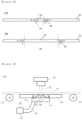
- FIG. 2 is a plan view illustrating an embodiment of a pattern jig used in an electrode manufacturing device according to the present invention
- FIG. 3 is a cross-sectional view of illustrating an A-A cross section (a) and a B-B cross section (b) of the pattern jig of FIG. 2
- FIG. 4 is a schematic cross-sectional view illustrating an embodiment of the electrode manufacturing device according to the present invention.
- the electrode manufacturing device 100 includes a transfer part 20 continuously transferring an electrode sheet 10 in order to perform an electrode notching process; a laser irradiation part 30 irradiating the electrode sheet 10 with a laser beam to perform the electrode notching process; and a pattern jig 40 positioned at a portion facing a laser irradiation part with the electrode sheet 10 interposed therebetween to support the electrode sheet, as illustrated in FIG. 4 , wherein the pattern jig 40 includes a panel 44 including a pattern hole 42 through which the laser beam that has notched the electrode sheet 10 passes, and the pattern hole 42 has a structure in which it becomes wide from the front toward the rear based on a laser beam traveling direction.
- the pattern jig 40 may be the panel 44 itself including the pattern hole 42, as illustrated in FIGS. 2 and 3 , and may further include a fixing part for fixing the panel 44 to a suction device or the like in addition to the panel 44.
- the fixing part may include a support member, a fixing means, and the like, for suitably fixing the panel 44 to the suction device or the like.
- the fixing means may be, for example, a coupling hole for screw coupling, or the like.
- the pattern hole 42 is formed as a through hole for the panel, and a wall 48 forming the through hole may include an inclined part forming an interior angle of 15° to 80°, preferably 15° to 70°, and more preferably 15° to 45° with an upper surface of the panel in a direction toward the laser irradiation part, as illustrated in FIG. 3 .
- the wall 48 may include an inclined part forming an interior angle of 10° to 75°, preferably 20° to 75°, and more preferably 45° to 75° based on an axis parallel to a central axis of the laser beam, as illustrated in FIG. 6 .
- the panel may have a thickness of 1.0 mm or less, preferably 0.7 mm or less, and more preferably 0.5 mm or less.
- the pattern jig 40 may be fixed to an upper portion of the suction device 50, as illustrated in FIGS. 4 and 9 . That is, in the electrode manufacturing device 100 according to the present invention, foreign substances (e.g., spatters) are generated at the time of notching of the electrode sheet 10 by the laser beam, and it is required to suck and remove such foreign substances. Accordingly, the pattern jig 40 may be installed together with the suction device.
- the suction device is installed in communication with the pattern hole 42 formed in the pattern jig 40, and performs a function of adsorbing foreign substances (e.g., spatters) generated in the pattern hole 42 and around the pattern hole by sucking air.
- the term "upper portion" refers to a position determined based on the laser beam traveling direction.
- the panel 44 including the pattern hole 42 may be a flat panel as illustrated in FIGS. 2 and 3 or a curved panel 44 convex in a direction toward the electrode sheet as illustrated in FIGS. 5 and 6.
- FIG. 5 is a perspective view illustrating another embodiment of the pattern jig used in the electrode manufacturing device according to the present invention
- FIG. 6 is a cross-sectional view of illustrating an A-A cross section of the pattern jig of FIG. 5 .
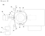
- the pattern jig 40 When the pattern jig 40 includes the curved panel 44 convex in the direction toward the electrode sheet, the pattern jig 40 may be applied to, for example, an electrode manufacturing device as illustrated in FIG. 9 . That is, the pattern jig 40 as described above may be used in a form in which it is fixed to, for example, a cylindrical drum suction 50 as illustrated in FIG. 9 .
- the transfer part 20 of the electrode sheet 10 supplies the electrode sheet 10 so that the electrode sheet 10 can pass through the cylindrical drum suction 50 while surrounding a portion of the cylindrical drum suction 50.
- the pattern jig 40 is fixed to a surface of the cylindrical drum suction 50 in contact with the electrode sheet 10, and electrode notching is performed by a laser beam 32 irradiated from the laser irradiation part 30.
- Three to ten pattern jigs 40 including the curved panel may be fixed to the cylindrical drum suction, and the electrode notching may be performed while the pattern jig 40 is replaced with another pattern jig 40 by rotation of the cylindrical drum suction 50 at the time of electrode notching.
- a foreign substance adhesion prevention coating layer may be further provided on a surface of the panel including the pattern hole.
- the foreign substance adhesion prevention coating layer may have a friction coefficient of 0.3 or less and preferably 0.15 or less and a surface roughness of 0.15 um or less and preferably 0.1 um or less.
- the foreign substance adhesion prevention coating layer may have a hardness of 1,800 to 2,000.
- the foreign substance adhesion prevention coating layer may be formed of one or more coatings selected from a diamond-like carbon (DLC) coating, an AlCrN (Alcrona) coating, and the like, but is not limited thereto, and a known coating material may be used without limitation as long as a coating satisfies a material of the coating layer.
- DLC diamond-like carbon
- AlCrN Alcrona
- the electrode sheet 10 may include a coated portion that is coated with an electrode active material and a non-coated portion that is not coated with the electrode active material, on one surface or both surfaces of an electrode current collector.
- the notching may be a process of notching an electrode tab or cutting the electrode into individual units.
- electrode sheet 20 transfer part 30: laser irradiation part 32: laser beam 34 : laser oscillation part 36 : suction part 40: pattern jig 42: pattern hole 44: panel 46: pattern jig fixing groove 48: pattern hole wall 49: coating layer 50: suction device 52: suction hole 54: suction pipe 56: suction device 100: electrode manufacturing device
Landscapes
- Engineering & Computer Science (AREA)
- Physics & Mathematics (AREA)
- Optics & Photonics (AREA)
- Mechanical Engineering (AREA)
- Chemical & Material Sciences (AREA)
- Plasma & Fusion (AREA)
- Chemical Kinetics & Catalysis (AREA)
- Electrochemistry (AREA)
- General Chemical & Material Sciences (AREA)
- Manufacturing & Machinery (AREA)
- Materials Engineering (AREA)
- Battery Electrode And Active Subsutance (AREA)
Abstract
Description
- This application claims the benefit of priority based on
Korean Patent Application No. 10-2021-0172820 filed on December 6, 2021 - The present invention relates to an electrode manufacturing device used for laser notching of an electrode.
- As the demand for mobile devices, electric vehicles, and the like increases, the demand for secondary batteries is rapidly increasing. In particular, lithium secondary batteries having high energy density and voltage among the secondary batteries have been commercialized and widely used.
- The lithium secondary batteries are also classified according to a structure of an electrode assembly having a structure in which a cathode, an anode, and a separator interposed between the cathode and the anode are stacked. Examples of the electrode assembly according to such classification may include a jelly-roll type (wound type) electrode assembly having a structure in which cathodes and anodes having a long sheet shape are rolled with separators interposed therebetween, a stack type (layered type) electrode assembly in which a plurality of cathodes and anodes cut in units of a predetermined size are sequentially stacked with separators interposed therebetween, and the like. Recently, in order to solve problems of the jelly-roll type electrode assembly and the stack type electrode assembly, a stack/folding type electrode assembly, having a form in which the jelly-roll type electrode assembly and the stack type electrode assembly are mixed and having a structure in which unit cells in which cathodes and anodes of a predetermined unit are stacked with separators interposed therebetween are sequentially rolled in a state in which they are positioned on separation films, is also used.
- Generally, such a secondary battery is completed by applying and drying electrode mixtures in which an electrode active material, a conductive agent, a binder, and the like are mixed on an electrode current collector to manufacture electrodes, stacking the manufactured electrodes together with a separator, and then embedding and sealing a laminate together with an electrolyte solution in a battery case.
- In this case, the electrode is manufactured by notching an electrode sheet manufactured by applying the electrode active material on the electrode current collector having a long sheet shape, and then cutting the electrode sheet at a predetermined length.
- Generally, a notching process is performed using a jig or a roller including a cutting part having a shape corresponding to the electrode. Recently, the notching process is also performed by a method of irradiating the electrode sheet with a predetermined laser so that the electrode can be formed in a more precise dimension.
- An electrode manufacturing device according to the related art using a laser is illustrated in
FIG. 1 . As illustrated inFIG. 1 , in the electrode manufacturing device according to the related art has a disadvantage of causing a problem that foreign substances (spatters, etc.) generated at the time of notching damage to an electrode sheet while being accumulated or stuck and piled up around apattern hole 42 of apattern jig 40. - Therefore, improvement on such a problem is required.
-
Korean Patent No. 10-2158708 - The present invention has been devised to solve the problem of the related art as described above, and
an object of the present invention is to provide an electrode manufacturing device capable of effectively preventing foreign substances (spatters, etc.) generated at the time of laser notching of an electrode from being accumulated and stuck around a pattern hole of a pattern jig to damage an electrode sheet. - In order to achieve the above object, the present invention provides an electrode manufacturing device, including:
- a transfer part continuously transferring an electrode sheet in order to perform an electrode notching process;
- a laser irradiation part irradiating the electrode sheet with a laser beam to perform the electrode notching process; and
- a pattern jig positioned at a portion facing a laser irradiation part with the electrode sheet interposed therebetween to support the electrode sheet,
- wherein the pattern jig includes a panel including a pattern hole through which the laser beam that has notched the electrode sheet passes, and the pattern hole has a structure in which it becomes wide from the front toward the rear based on a laser beam traveling direction.
- In an embodiment of the present invention, the pattern hole may be formed as a through hole for the panel, and a wall forming the through hole may include an inclined part forming an interior angle of 15° to 80° with an upper surface of the panel in a direction toward the laser irradiation part. Preferably, a wall forming the through hole may include an inclined part an interior angle of 15° to 70° with an upper surface of the panel in a direction toward the laser irradiation part.
- In an embodiment of the present invention, the panel may have a thickness of 1.0 mm or less.
- In an embodiment of the present invention, the panel including the pattern hole may be a flat panel or a curved panel convex in a direction toward the electrode sheet.
- In an embodiment of the present invention, the pattern jig may be fixed to an upper portion of a suction device.
- In an embodiment of the present invention, the panel including the pattern hole may be the curved panel convex in the direction toward the electrode sheet, and the pattern jig including the curved panel may be fixed to a cylindrical drum suction.
- In an embodiment of the present invention, three to ten pattern jigs including the convex curved panel may be fixed to the cylindrical drum suction, and electrode notching may be performed while the pattern jig is replaced with another pattern jig by rotation of the cylindrical drum suction at the time of electrode notching.
- In an embodiment of the present invention, a foreign substance adhesion prevention coating layer may be further provided on a surface of the panel including the pattern hole.
- The foreign substance adhesion prevention coating layer may have a friction coefficient of 0.3 or less and a surface roughness of 0.15 um or less.
- In an embodiment of the present invention, the foreign substance adhesion prevention coating layer may be formed of one or more coatings selected from a diamond-like carbon (DLC) coating, an AlCrN (Alcrona) coating.
- In an embodiment of the present invention, the electrode sheet may include a coated portion that is coated with an electrode active material and a non-coated portion that is not coated with the electrode active material, on one surface or both surfaces of an electrode current collector.
- In an embodiment of the present invention, the electrode manufacturing device may be used in a notching process for forming an electrode tab.
- An electrode manufacturing device according to the present invention includes a pattern jig having an improved structure, and thus, may effectively prevent foreign substances (spatters, etc.) generated at the time of laser notching of an electrode from being accumulated and stuck around a pattern hole of the pattern jig to damage an electrode sheet.
-
-
FIG. 1 is a schematic cross-sectional view illustrating an electrode manufacturing device according to the related art and a use state thereof. -
FIG. 2 is a plan view illustrating an embodiment of a pattern jig used in an electrode manufacturing device according to the present invention. -
FIG. 3 is a cross-sectional view of illustrating an A-A cross section (a) and a B-B cross section (b) of the pattern jig ofFIG. 2 . -
FIG. 4 is a schematic cross-sectional view illustrating an embodiment of the electrode manufacturing device according to the present invention. -
FIG. 5 is a perspective view illustrating another embodiment of the pattern jig used in the electrode manufacturing device according to the present invention. -
FIG. 6 is a cross-sectional view of illustrating an A-A cross section of the pattern jig ofFIG. 5 . -
FIG. 7 is a schematic cross-sectional view illustrating another embodiment of the electrode manufacturing device according to the present invention. -
FIG. 8 is a photograph illustrating another embodiment of the pattern jig used in the electrode manufacturing device according to the present invention. -
FIG. 9 is a schematic cross-sectional view illustrating another embodiment of the electrode manufacturing device according to the present invention. -
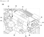
FIG. 10 is a schematic perspective view illustrating another embodiment of the electrode manufacturing device according to the present invention. - Hereinafter, embodiments of the present invention will be described in detail with reference to the accompanying drawings so that those skilled in the art to which the present invention pertains may easily practice the present invention. However, the present invention may be implemented in various different forms, and is not limited to embodiments described herein. Throughout the specification, similar parts will be denoted by the same reference numerals.
-
FIG. 2 is a plan view illustrating an embodiment of a pattern jig used in an electrode manufacturing device according to the present invention,FIG. 3 is a cross-sectional view of illustrating an A-A cross section (a) and a B-B cross section (b) of the pattern jig ofFIG. 2 , andFIG. 4 is a schematic cross-sectional view illustrating an embodiment of the electrode manufacturing device according to the present invention. - The
electrode manufacturing device 100 according to the present invention includes atransfer part 20 continuously transferring anelectrode sheet 10 in order to perform an electrode notching process; alaser irradiation part 30 irradiating theelectrode sheet 10 with a laser beam to perform the electrode notching process; and apattern jig 40 positioned at a portion facing a laser irradiation part with theelectrode sheet 10 interposed therebetween to support the electrode sheet, as illustrated inFIG. 4 ,
wherein thepattern jig 40 includes apanel 44 including apattern hole 42 through which the laser beam that has notched theelectrode sheet 10 passes, and thepattern hole 42 has a structure in which it becomes wide from the front toward the rear based on a laser beam traveling direction. - The
pattern jig 40 may be thepanel 44 itself including thepattern hole 42, as illustrated inFIGS. 2 and3 , and may further include a fixing part for fixing thepanel 44 to a suction device or the like in addition to thepanel 44. The fixing part may include a support member, a fixing means, and the like, for suitably fixing thepanel 44 to the suction device or the like. The fixing means may be, for example, a coupling hole for screw coupling, or the like. - In an embodiment of the present invention, the
pattern hole 42 is formed as a through hole for the panel, and awall 48 forming the through hole may include an inclined part forming an interior angle of 15° to 80°, preferably 15° to 70°, and more preferably 15° to 45° with an upper surface of the panel in a direction toward the laser irradiation part, as illustrated inFIG. 3 . - Meanwhile, the
wall 48 may include an inclined part forming an interior angle of 10° to 75°, preferably 20° to 75°, and more preferably 45° to 75° based on an axis parallel to a central axis of the laser beam, as illustrated inFIG. 6 . - In an embodiment of the present invention, the panel may have a thickness of 1.0 mm or less, preferably 0.7 mm or less, and more preferably 0.5 mm or less.
- In an embodiment of the present invention, the
pattern jig 40 may be fixed to an upper portion of thesuction device 50, as illustrated inFIGS. 4 and9 . That is, in theelectrode manufacturing device 100 according to the present invention, foreign substances (e.g., spatters) are generated at the time of notching of theelectrode sheet 10 by the laser beam, and it is required to suck and remove such foreign substances. Accordingly, thepattern jig 40 may be installed together with the suction device. The suction device is installed in communication with thepattern hole 42 formed in thepattern jig 40, and performs a function of adsorbing foreign substances (e.g., spatters) generated in thepattern hole 42 and around the pattern hole by sucking air. In the above, the term "upper portion" refers to a position determined based on the laser beam traveling direction. - In an embodiment of the present invention, the
panel 44 including thepattern hole 42 may be a flat panel as illustrated inFIGS. 2 and3 or acurved panel 44 convex in a direction toward the electrode sheet as illustrated inFIGS. 5 and 6. FIG. 5 is a perspective view illustrating another embodiment of the pattern jig used in the electrode manufacturing device according to the present invention, andFIG. 6 is a cross-sectional view of illustrating an A-A cross section of the pattern jig ofFIG. 5 . - When the
pattern jig 40 includes thecurved panel 44 convex in the direction toward the electrode sheet, thepattern jig 40 may be applied to, for example, an electrode manufacturing device as illustrated inFIG. 9 . That is, thepattern jig 40 as described above may be used in a form in which it is fixed to, for example, acylindrical drum suction 50 as illustrated inFIG. 9 . - In the electrode manufacturing device illustrated in
FIG. 9 , thetransfer part 20 of theelectrode sheet 10 supplies theelectrode sheet 10 so that theelectrode sheet 10 can pass through thecylindrical drum suction 50 while surrounding a portion of thecylindrical drum suction 50. In this case, thepattern jig 40 is fixed to a surface of thecylindrical drum suction 50 in contact with theelectrode sheet 10, and electrode notching is performed by alaser beam 32 irradiated from thelaser irradiation part 30. - Three to ten pattern jigs 40 including the curved panel may be fixed to the cylindrical drum suction, and the electrode notching may be performed while the
pattern jig 40 is replaced with anotherpattern jig 40 by rotation of thecylindrical drum suction 50 at the time of electrode notching. - In an embodiment of the present invention, a foreign substance adhesion prevention coating layer may be further provided on a surface of the panel including the pattern hole.
- The foreign substance adhesion prevention coating layer may have a friction coefficient of 0.3 or less and preferably 0.15 or less and a surface roughness of 0.15 um or less and preferably 0.1 um or less.
- When the friction coefficient exceeds 0.3, foreign substances may be accumulated or stuck, which is not preferable. In addition, when the surface roughness exceeds 0.15 um, foreign substances may be accumulated or stuck, which is not preferable.
- The foreign substance adhesion prevention coating layer may have a hardness of 1,800 to 2,000.
- The foreign substance adhesion prevention coating layer may be formed of one or more coatings selected from a diamond-like carbon (DLC) coating, an AlCrN (Alcrona) coating, and the like, but is not limited thereto, and a known coating material may be used without limitation as long as a coating satisfies a material of the coating layer.
- In an embodiment of the present invention, the
electrode sheet 10 may include a coated portion that is coated with an electrode active material and a non-coated portion that is not coated with the electrode active material, on one surface or both surfaces of an electrode current collector. - In an embodiment of the present invention, the notching may be a process of notching an electrode tab or cutting the electrode into individual units.
- Although the present invention has been described in relation to the above-described embodiments,
- various modifications and alterations may be made without departing from the gist and scope of the present invention. Accordingly, these modifications and alterations fall within the scope of the claims as long as they belong to the gist of the present invention.
-
10: electrode sheet 20: transfer part 30: laser irradiation part 32: laser beam 34 : laser oscillation part 36 : suction part 40: pattern jig 42: pattern hole 44: panel 46: pattern jig fixing groove 48: pattern hole wall 49: coating layer 50: suction device 52: suction hole 54: suction pipe 56: suction device 100: electrode manufacturing device
Claims (13)
- An electrode manufacturing device, comprising:a transfer part continuously transferring an electrode sheet in order to perform an electrode notching process;a laser irradiation part irradiating the electrode sheet with a laser beam to perform the electrode notching process; anda pattern jig positioned at a portion facing the laser irradiation part with the electrode sheet interposed therebetween to support the electrode sheet,wherein the pattern jig includes a panel having a pattern hole through which the laser beam passes, the pattern hole having width that increases in a direction the laser beam travels.
- The electrode manufacturing device of claim 1, wherein the pattern hole is formed as a through hole for the panel, and a wall forming the through hole includes an inclined part forming an interior angle of 15° to 80° with an upper surface of the panel in a direction toward the laser irradiation part.
- The electrode manufacturing device of claim 1, wherein a wall forming the through hole forms an interior angle of 15° to 70° with an upper surface of the panel in a direction toward the laser irradiation part.
- The electrode manufacturing device of claim 1, wherein the panel has a thickness of 1.0 mm or less.
- The electrode manufacturing device of claim 1, wherein the panel comprising the pattern hole is a flat panel or a curved panel convex in a direction toward the electrode sheet.
- The electrode manufacturing device of claim 1, wherein the pattern jig is fixed to an upper portion of a suction device.
- The electrode manufacturing device of claim 5, wherein the panel comprising the pattern hole is the curved panel convex in the direction toward the electrode sheet, and the pattern jig comprising the curved panel is fixed to a cylindrical drum suction.
- The electrode manufacturing device of claim 7, wherein three to ten pattern jigs comprising the curved panel convex in the direction toward the electrode sheet are fixed to the cylindrical drum suction, and electrode notching is performed while the pattern jig is replaced with another pattern jig by rotation of the cylindrical drum suction at the time of electrode notching.
- The electrode manufacturing device of claim 1, wherein a foreign substance adhesion prevention coating layer is further provided on a surface of the panel including the pattern hole.
- The electrode manufacturing device of claim 9, wherein the foreign substance adhesion prevention coating layer has a friction coefficient of 0.3 or less and a surface roughness of 0.15 um or less.
- The electrode manufacturing device of claim 9, wherein the foreign substance adhesion prevention coating layer is formed of one or more coatings selected from a diamond-like carbon (DLC) coating and an AlCrN coating.
- The electrode manufacturing device of claim 1, wherein the electrode sheet comprises a coated portion that is coated with an electrode active material and a non-coated portion that is not coated with the electrode active material, on one surface or both surfaces of an electrode current collector.
- The electrode manufacturing device of claim 1, wherein the electrode manufacturing device is used in a notching process for forming an electrode tab.
Applications Claiming Priority (2)
| Application Number | Priority Date | Filing Date | Title |
|---|---|---|---|
| KR1020210172820A KR102904726B1 (en) | 2021-12-06 | 2021-12-06 | Electrode manufacturing device used for laser notching of electrodes |
| PCT/KR2022/019590 WO2023106755A1 (en) | 2021-12-06 | 2022-12-05 | Electrode manufacturing device used for laser notching of electrode |
Publications (2)
| Publication Number | Publication Date |
|---|---|
| EP4342623A1 true EP4342623A1 (en) | 2024-03-27 |
| EP4342623A4 EP4342623A4 (en) | 2025-06-04 |
Family
ID=86730863
Family Applications (1)
| Application Number | Title | Priority Date | Filing Date |
|---|---|---|---|
| EP22904585.1A Pending EP4342623A4 (en) | 2021-12-06 | 2022-12-05 | Electrode manufacturing device used for laser notching of electrode |
Country Status (6)
| Country | Link |
|---|---|
| US (1) | US20240246177A1 (en) |
| EP (1) | EP4342623A4 (en) |
| JP (1) | JP7665919B2 (en) |
| KR (1) | KR102904726B1 (en) |
| CN (1) | CN117580673A (en) |
| WO (1) | WO2023106755A1 (en) |
Families Citing this family (7)
| Publication number | Priority date | Publication date | Assignee | Title |
|---|---|---|---|---|
| KR20250066285A (en) * | 2023-11-06 | 2025-05-13 | 주식회사 엘지에너지솔루션 | Electrode nothing device and electrode nothing method using the same |
| IT202300027669A1 (en) * | 2023-12-21 | 2025-06-21 | Fameccanica Data Spa | LASER CUTTING DEVICE AND RELATED PROCEDURE |
| CN120660197A (en) * | 2023-12-26 | 2025-09-16 | 株式会社Lg新能源 | Electrode production device and battery cell including electrode produced by the same, and battery pack and vehicle including the battery cell |
| EP4645405A1 (en) * | 2023-12-26 | 2025-11-05 | LG Energy Solution, Ltd. | Electrode production apparatus and battery cells comprising electrodes produced thereby, and battery pack and vehicle comprising battery cells |
| KR20250147410A (en) * | 2024-04-04 | 2025-10-13 | 주식회사 엘지에너지솔루션 | Laser notching apparatus |
| KR20260019236A (en) * | 2024-08-01 | 2026-02-10 | 주식회사 엘지에너지솔루션 | Jig cleaning device, jig cleaning method, electrode manufcturing device and electrode manufcturing method |
| KR102899072B1 (en) * | 2025-02-18 | 2025-12-11 | 주식회사 풍산홀딩스 | Dust treatment device in secondary battery lead tab production system |
Family Cites Families (13)
| Publication number | Priority date | Publication date | Assignee | Title |
|---|---|---|---|---|
| FR2853772B1 (en) * | 2003-04-08 | 2005-07-01 | Production Et De Rech S Appliq | CONTROL OF THE SPATIO-TEMPORAL UNIFORMITY OF THE BEAM OF A PULSED GAS LASER |
| JP2005340228A (en) * | 2004-05-24 | 2005-12-08 | Tdk Corp | Manufacturing method and apparatus of electrochemical element |
| CN101249586A (en) * | 2008-04-15 | 2008-08-27 | 昆明理工大学 | Device and method for online laser cutting tipping paper |
| KR20150102771A (en) * | 2013-10-30 | 2015-09-08 | 주식회사 엘지화학 | Apparatus for cutting an electrode using laser and electrode supply method of the same |
| KR101774262B1 (en) * | 2015-03-11 | 2017-09-04 | 주식회사 엘지화학 | Electrode Tab Fabricating Apparatus with Improved Dimensional Stability and Method for Fabricating Electrode Tab Utilizing the Same |
| DE102015218650B3 (en) * | 2015-06-12 | 2016-10-20 | Schuler Automation Gmbh & Co. Kg | Device for cutting sheet metal blanks from a sheet metal strip |
| KR101713226B1 (en) * | 2016-04-28 | 2017-03-07 | 이권열 | Manufacturing method of gas welding torch's welding nozzle |
| CN105728957A (en) * | 2016-05-11 | 2016-07-06 | 张澎涛 | Processing method and processing device for pocket hole of carrier band of miniature electronic component |
| EP3415265B1 (en) * | 2017-06-12 | 2020-12-30 | Robert Bosch GmbH | Method and device for high-throughput cutting of a ribbon-type substrate, particularly for an electrode of a battery, into separated pieces |
| DE102017216133A1 (en) * | 2017-09-13 | 2019-03-14 | Robert Bosch Gmbh | Method for separating ribbon-shaped electrode and separator material on a curved surface |
| CN208467531U (en) * | 2018-03-28 | 2019-02-05 | 景旺电子科技(龙川)有限公司 | A universal auxiliary fixture for drilling |
| KR102158708B1 (en) | 2020-06-10 | 2020-09-22 | 주식회사 디에이테크놀로지 | Drum Type Pattern Jig for Laser Notching Process of Electrode Film for Secondary Battery, And Laser Notching System Having the Pattern Jig |
| KR102245162B1 (en) * | 2020-08-11 | 2021-04-27 | 주식회사 디에이테크놀로지 | System for Laser Notching Process of Secondary Battery Electrode Film |
-
2021
- 2021-12-06 KR KR1020210172820A patent/KR102904726B1/en active Active
-
2022
- 2022-12-05 JP JP2023576183A patent/JP7665919B2/en active Active
- 2022-12-05 US US18/578,128 patent/US20240246177A1/en active Pending
- 2022-12-05 CN CN202280046014.XA patent/CN117580673A/en active Pending
- 2022-12-05 WO PCT/KR2022/019590 patent/WO2023106755A1/en not_active Ceased
- 2022-12-05 EP EP22904585.1A patent/EP4342623A4/en active Pending
Also Published As
| Publication number | Publication date |
|---|---|
| JP7665919B2 (en) | 2025-04-22 |
| KR102904726B1 (en) | 2025-12-24 |
| KR20230084777A (en) | 2023-06-13 |
| CN117580673A (en) | 2024-02-20 |
| US20240246177A1 (en) | 2024-07-25 |
| JP2024523260A (en) | 2024-06-28 |
| EP4342623A4 (en) | 2025-06-04 |
| WO2023106755A1 (en) | 2023-06-15 |
Similar Documents
| Publication | Publication Date | Title |
|---|---|---|
| US20240246177A1 (en) | Electrode Manufacturing Device Used For Laser Notching Of Electrode | |
| KR102182307B1 (en) | Device for Manufacturing Electrode Comprising Pattern Zig and Scrap Outlet Portion | |
| KR20230109896A (en) | Electrode tab notching device | |
| US20170098857A1 (en) | Coated stacks for batteries and related manufacturing methods | |
| CN109689365B (en) | Leveling apparatus for preventing pouch type secondary battery from curling | |
| EP4106035B1 (en) | Electrode assembly comprising anode and anode sheet having improved electrode stacking properties and manufacturing method therefor | |
| US12337494B2 (en) | Method and apparatus for manufacturing unit cells | |
| KR20240017892A (en) | Electrode assembly | |
| EP4109612B1 (en) | Unit cell manufacturing apparatus and method | |
| KR20230013621A (en) | electrode sheet processing method and apparatus | |
| KR20230055782A (en) | Notching system for electrode sheet | |
| KR102914055B1 (en) | The Apparatus And The Method For Manufacturing Unit Cell | |
| US20260005283A1 (en) | Power Supply Device, Device for Manufacturing Electrode Assembly Using Same, Electrode Supply Method, and Method for Manufacturing Electrode Assembly Using Same | |
| KR20220021841A (en) | A method of manufacturing an electrode assembly comprising a anode and a anode having improved electrode stacking characteristics | |
| KR102608542B1 (en) | Manufacturing method for electrode assembly and electrode assembly manufacturing equipment | |
| KR20230032989A (en) | Electrode driving roller and notching device comprising the same | |
| KR20230123233A (en) | Electrode slitting device | |
| EP4645404A1 (en) | Electrode production apparatus and battery cells comprising electrodes produced thereby, and battery pack and vehicle comprising battery cells | |
| US20260108987A1 (en) | Laser notching apparatus and rechargeable battery manufacturing system | |
| KR102876298B1 (en) | Jelly-Roll Electrode Assembly and Secondary Battery Comprising the Same | |
| EP4428972A1 (en) | Plasma processing apparatus and lamination system for secondary battery comprising same | |
| US20240170643A1 (en) | Method of fabricating a pre-lithiated electrode and lithium-ion battery cell | |
| KR20260039199A (en) | Metal Foreign Matter Removal Device for Electrode Sheet | |
| KR20240054791A (en) | Electrode assembly manufacturing method with improved processability and electrode assembly manufactured by using the same | |
| KR20250167438A (en) | Notching tab scrap suction apparatus |
Legal Events
| Date | Code | Title | Description |
|---|---|---|---|
| STAA | Information on the status of an ep patent application or granted ep patent |
Free format text: STATUS: THE INTERNATIONAL PUBLICATION HAS BEEN MADE |
|
| PUAI | Public reference made under article 153(3) epc to a published international application that has entered the european phase |
Free format text: ORIGINAL CODE: 0009012 |
|
| STAA | Information on the status of an ep patent application or granted ep patent |
Free format text: STATUS: REQUEST FOR EXAMINATION WAS MADE |
|
| 17P | Request for examination filed |
Effective date: 20231218 |
|
| AK | Designated contracting states |
Kind code of ref document: A1 Designated state(s): AL AT BE BG CH CY CZ DE DK EE ES FI FR GB GR HR HU IE IS IT LI LT LU LV MC ME MK MT NL NO PL PT RO RS SE SI SK SM TR |
|
| DAV | Request for validation of the european patent (deleted) | ||
| DAX | Request for extension of the european patent (deleted) | ||
| A4 | Supplementary search report drawn up and despatched |
Effective date: 20250508 |
|
| RIC1 | Information provided on ipc code assigned before grant |
Ipc: B23K 101/36 20060101ALI20250501BHEP Ipc: H01M 50/531 20210101ALI20250501BHEP Ipc: H01M 4/04 20060101ALI20250501BHEP Ipc: B23K 26/362 20140101AFI20250501BHEP |
|
| GRAP | Despatch of communication of intention to grant a patent |
Free format text: ORIGINAL CODE: EPIDOSNIGR1 |
|
| STAA | Information on the status of an ep patent application or granted ep patent |
Free format text: STATUS: GRANT OF PATENT IS INTENDED |
|
| INTG | Intention to grant announced |
Effective date: 20260220 |
|
| P01 | Opt-out of the competence of the unified patent court (upc) registered |
Free format text: CASE NUMBER: UPC_APP_0009379_4342623/2026 Effective date: 20260311 |
|
| GRAS | Grant fee paid |
Free format text: ORIGINAL CODE: EPIDOSNIGR3 |
|
| GRAA | (expected) grant |
Free format text: ORIGINAL CODE: 0009210 |
|
| STAA | Information on the status of an ep patent application or granted ep patent |
Free format text: STATUS: THE PATENT HAS BEEN GRANTED |