EP4340554A1 - Thermal management for flat no lead packages - Google Patents
Thermal management for flat no lead packages Download PDFInfo
- Publication number
- EP4340554A1 EP4340554A1 EP23196896.7A EP23196896A EP4340554A1 EP 4340554 A1 EP4340554 A1 EP 4340554A1 EP 23196896 A EP23196896 A EP 23196896A EP 4340554 A1 EP4340554 A1 EP 4340554A1
- Authority
- EP
- European Patent Office
- Prior art keywords
- pcb
- housing
- thermal
- flat
- package
- Prior art date
- Legal status (The legal status is an assumption and is not a legal conclusion. Google has not performed a legal analysis and makes no representation as to the accuracy of the status listed.)
- Pending
Links
Images


Classifications
-
- H—ELECTRICITY
- H05—ELECTRIC TECHNIQUES NOT OTHERWISE PROVIDED FOR
- H05K—PRINTED CIRCUITS; CASINGS OR CONSTRUCTIONAL DETAILS OF ELECTRIC APPARATUS; MANUFACTURE OF ASSEMBLAGES OF ELECTRICAL COMPONENTS
- H05K1/00—Printed circuits
- H05K1/18—Printed circuits structurally associated with non-printed electric components
-
- H—ELECTRICITY
- H05—ELECTRIC TECHNIQUES NOT OTHERWISE PROVIDED FOR
- H05K—PRINTED CIRCUITS; CASINGS OR CONSTRUCTIONAL DETAILS OF ELECTRIC APPARATUS; MANUFACTURE OF ASSEMBLAGES OF ELECTRICAL COMPONENTS
- H05K3/00—Apparatus or processes for manufacturing printed circuits
- H05K3/30—Assembling printed circuits with electric components, e.g. with resistors
- H05K3/32—Assembling printed circuits with electric components, e.g. with resistors electrically connecting electric components or wires to printed circuits
- H05K3/34—Assembling printed circuits with electric components, e.g. with resistors electrically connecting electric components or wires to printed circuits by soldering
- H05K3/341—Surface mounted components
- H05K3/3431—Leadless components
- H05K3/3442—Leadless components having edge contacts, e.g. leadless chip capacitors, chip carriers
-
- H—ELECTRICITY
- H05—ELECTRIC TECHNIQUES NOT OTHERWISE PROVIDED FOR
- H05K—PRINTED CIRCUITS; CASINGS OR CONSTRUCTIONAL DETAILS OF ELECTRIC APPARATUS; MANUFACTURE OF ASSEMBLAGES OF ELECTRICAL COMPONENTS
- H05K1/00—Printed circuits
- H05K1/02—Details
- H05K1/0201—Thermal arrangements, e.g. for cooling, heating or preventing overheating
- H05K1/0203—Cooling of mounted components
-
- H—ELECTRICITY
- H05—ELECTRIC TECHNIQUES NOT OTHERWISE PROVIDED FOR
- H05K—PRINTED CIRCUITS; CASINGS OR CONSTRUCTIONAL DETAILS OF ELECTRIC APPARATUS; MANUFACTURE OF ASSEMBLAGES OF ELECTRICAL COMPONENTS
- H05K3/00—Apparatus or processes for manufacturing printed circuits
- H05K3/30—Assembling printed circuits with electric components, e.g. with resistors
- H05K3/32—Assembling printed circuits with electric components, e.g. with resistors electrically connecting electric components or wires to printed circuits
-
- H—ELECTRICITY
- H05—ELECTRIC TECHNIQUES NOT OTHERWISE PROVIDED FOR
- H05K—PRINTED CIRCUITS; CASINGS OR CONSTRUCTIONAL DETAILS OF ELECTRIC APPARATUS; MANUFACTURE OF ASSEMBLAGES OF ELECTRICAL COMPONENTS
- H05K3/00—Apparatus or processes for manufacturing printed circuits
- H05K3/30—Assembling printed circuits with electric components, e.g. with resistors
- H05K3/32—Assembling printed circuits with electric components, e.g. with resistors electrically connecting electric components or wires to printed circuits
- H05K3/34—Assembling printed circuits with electric components, e.g. with resistors electrically connecting electric components or wires to printed circuits by soldering
- H05K3/341—Surface mounted components
- H05K3/3421—Leaded components
- H05K3/3426—Leaded components characterised by the leads
-
- H—ELECTRICITY
- H10—SEMICONDUCTOR DEVICES; ELECTRIC SOLID-STATE DEVICES NOT OTHERWISE PROVIDED FOR
- H10W—GENERIC PACKAGES, INTERCONNECTIONS, CONNECTORS OR OTHER CONSTRUCTIONAL DETAILS OF DEVICES COVERED BY CLASS H10
- H10W40/00—Arrangements for thermal protection or thermal control
-
- H—ELECTRICITY
- H10—SEMICONDUCTOR DEVICES; ELECTRIC SOLID-STATE DEVICES NOT OTHERWISE PROVIDED FOR
- H10W—GENERIC PACKAGES, INTERCONNECTIONS, CONNECTORS OR OTHER CONSTRUCTIONAL DETAILS OF DEVICES COVERED BY CLASS H10
- H10W40/00—Arrangements for thermal protection or thermal control
- H10W40/20—Arrangements for cooling
- H10W40/22—Arrangements for cooling characterised by their shape, e.g. having conical or cylindrical projections
-
- H—ELECTRICITY
- H10—SEMICONDUCTOR DEVICES; ELECTRIC SOLID-STATE DEVICES NOT OTHERWISE PROVIDED FOR
- H10W—GENERIC PACKAGES, INTERCONNECTIONS, CONNECTORS OR OTHER CONSTRUCTIONAL DETAILS OF DEVICES COVERED BY CLASS H10
- H10W74/00—Encapsulations, e.g. protective coatings
- H10W74/10—Encapsulations, e.g. protective coatings characterised by their shape or disposition
- H10W74/111—Encapsulations, e.g. protective coatings characterised by their shape or disposition the semiconductor body being completely enclosed
- H10W74/114—Encapsulations, e.g. protective coatings characterised by their shape or disposition the semiconductor body being completely enclosed by a substrate and the encapsulations
-
- H—ELECTRICITY
- H05—ELECTRIC TECHNIQUES NOT OTHERWISE PROVIDED FOR
- H05K—PRINTED CIRCUITS; CASINGS OR CONSTRUCTIONAL DETAILS OF ELECTRIC APPARATUS; MANUFACTURE OF ASSEMBLAGES OF ELECTRICAL COMPONENTS
- H05K2201/00—Indexing scheme relating to printed circuits covered by H05K1/00
- H05K2201/10—Details of components or other objects attached to or integrated in a printed circuit board
- H05K2201/10431—Details of mounted components
- H05K2201/10439—Position of a single component
- H05K2201/10477—Inverted
-
- H—ELECTRICITY
- H05—ELECTRIC TECHNIQUES NOT OTHERWISE PROVIDED FOR
- H05K—PRINTED CIRCUITS; CASINGS OR CONSTRUCTIONAL DETAILS OF ELECTRIC APPARATUS; MANUFACTURE OF ASSEMBLAGES OF ELECTRICAL COMPONENTS
- H05K2201/00—Indexing scheme relating to printed circuits covered by H05K1/00
- H05K2201/10—Details of components or other objects attached to or integrated in a printed circuit board
- H05K2201/10431—Details of mounted components
- H05K2201/10507—Involving several components
- H05K2201/10515—Stacked components
-
- H—ELECTRICITY
- H05—ELECTRIC TECHNIQUES NOT OTHERWISE PROVIDED FOR
- H05K—PRINTED CIRCUITS; CASINGS OR CONSTRUCTIONAL DETAILS OF ELECTRIC APPARATUS; MANUFACTURE OF ASSEMBLAGES OF ELECTRICAL COMPONENTS
- H05K2201/00—Indexing scheme relating to printed circuits covered by H05K1/00
- H05K2201/10—Details of components or other objects attached to or integrated in a printed circuit board
- H05K2201/10613—Details of electrical connections of non-printed components, e.g. special leads
- H05K2201/10621—Components characterised by their electrical contacts
- H05K2201/10636—Leadless chip, e.g. chip capacitor or resistor
-
- H—ELECTRICITY
- H05—ELECTRIC TECHNIQUES NOT OTHERWISE PROVIDED FOR
- H05K—PRINTED CIRCUITS; CASINGS OR CONSTRUCTIONAL DETAILS OF ELECTRIC APPARATUS; MANUFACTURE OF ASSEMBLAGES OF ELECTRICAL COMPONENTS
- H05K2201/00—Indexing scheme relating to printed circuits covered by H05K1/00
- H05K2201/10—Details of components or other objects attached to or integrated in a printed circuit board
- H05K2201/10613—Details of electrical connections of non-printed components, e.g. special leads
- H05K2201/10742—Details of leads
- H05K2201/10886—Other details
- H05K2201/10946—Leads attached onto leadless component after manufacturing the component
-
- H—ELECTRICITY
- H05—ELECTRIC TECHNIQUES NOT OTHERWISE PROVIDED FOR
- H05K—PRINTED CIRCUITS; CASINGS OR CONSTRUCTIONAL DETAILS OF ELECTRIC APPARATUS; MANUFACTURE OF ASSEMBLAGES OF ELECTRICAL COMPONENTS
- H05K2203/00—Indexing scheme relating to apparatus or processes for manufacturing printed circuits covered by H05K3/00
- H05K2203/04—Soldering or other types of metallurgic bonding
- H05K2203/049—Wire bonding
Definitions
- Exemplary embodiments pertain to the art of heat management of electronics and, in particular, to managing heat for flat, no lead packages such as QFNs and DFNs.
- CCAs circuit card assembly
- a method of forming a circuit board assembly includes receiving a flat no-lead package.
- the package includes: a housing having a first side and second side; a circuit disposed within the housing; and an exposed thermal belly pad that is thermally coupled to the circuit and passes at least partially through the first side such that it can be exposed to an environment outside of the housing.
- the method also includes attaching the second side of the flat no-lead package to a first side of a printed circuit board (PCB) such that the exposed thermal belly pad is opposite the first side of the PCB.
- PCB printed circuit board
- the method can further include attaching a heat sink to the exposed thermal belly pad.
- the heat sink is a finned heat sink.
- the heat sink is attached by a thermal paste.
- the method can further include attaching a post to the exposed thermal belly pad.
- the method can further include: putting the PCB in a housing; and thermally connecting the post the housing.
- the post can be attached by a thermal paste.
- the PCB can include traces thereon and the method can further include electrically connecting the flat no-lead package to the traces.
- a circuit board assembly that includes: a flat no-lead package, wherein the package includes: a housing having a first side and second side; a circuit disposed within the housing; and an exposed thermal belly pad that is thermally coupled to the circuit and that passes at least partially through the first side; and a printed circuit board (PCB) having traces formed on a first side thereof, wherein the flat no-lead package is attached to a first side of the PCB such that the exposed thermal belly pad is opposite the first side of the PCB.
- PCB printed circuit board
- the assembly can further include a heat sink attached to the exposed thermal belly pad.
- the heat sink can be a finned heat sink.
- the heat sink is a finned heat sink.
- the heat sink is attached by a thermal paste.
- the assembly can further include a post attached to the exposed thermal belly pad.
- the assembly can further include a housing surrounding the PCB and the post can be thermally connected to the housing.
- the post can be attached by a thermal paste.
- thermal pad also known as a belly pad
- the terminal pads and thermal belly pads were typically placed on or near the surface of substrate that is part of a printed circuit board (PCB).
- PCB printed circuit board
- a configuration can lead to as disclosed above are systems (e.g., PCB's with flat no lead packages on them) where the flat no lead package is arranged such that the thermal belly pad and the terminal pads of the package are on the side of the package opposite the PCB.
- a heat sink feature such as fin or a post can be thermally connected to the thermal belly pad to improve heat dissipation.
- FIG. 1 shows an example of flat, no lead package 100.
- the package 100 includes a body/housing 102.
- the body/housing 102 surrounds one or more circuits that are not shown but the skilled artisan will realize that all packages herein include one or more circuits therein.
- the housing 102 includes four sides 120a-120d in FIG. 1 and all four sides include one or more openings 104 formed therein.
- the package 100 is a QFN. Of course, only two of sides (e.g., 120a and 120c) may include the openings 104. In such a case, the package may be a DFN. Regardless, herein, the package 100 can include openings in 1, 2, 3 or 4 sides.
- the openings 104 are holes or slots that expose terminal pads 106 so that electrical communication (e.g., power/data) can be conducted with the circuits inside the package 100.
- the terminal pads can be connected to a lead frame (not shown) as is known in the art.
- the package 100 can include a die that is surrounded by the lead frame.
- the lead frame is made up of a conductive material.
- the frame can be connected to the die by wire bonds.
- the terminal pads 106 are electrically connected to the lead frame and allow the die to be electrically connected to a printed circuit board.
- the package 100 includes a first or bottom side 110 and a second or top side 112.
- the package 100 includes an exposed thermal belly pad 108 that passes at least the first side 110 and is exposed to an environment outside of the housing 100.
- the pad 108 can be an outer surface of the first side 110, level with it or slightly above it. This pad 108 provides an efficient heat path from inside the package to outside the package. In the prior art, the pad was connected thermally to the PCB.
- FIG. 2 shows one example of how the package 100 can be arranged on a PCB 202 to form an assembly 200.
- the PCB 202 can include one or more traces 204 formed thereon.
- the traces 204 can be formed of a conductive such as a metal (e.g., copper) and can be used to route electrical signals and power within and between devices connected to the PCB.
- the PCB 202 can include a substrate 203 that is formed of a rigid or flexible materials depending on the intended PCB design. Rigid materials can include but are not limited to FR4 or polyimide fiberglass, while flexible circuits and rigid-flex flexible layers typically use high-temperature polyimide films. Common plastic substrates for flexible circuits include polyimide (PI), liquid crystal polymer (LCP), polyester (PET), and polyethylene naphthalate (PEN)
- PI polyimide
- LCP liquid crystal polymer
- PET polyester
- PEN polyethylene naphthalate
- the substrate 203 as is known in the art provides a non-conductive base onto which the traces 204 can be deposited.
- the substrate 203 also served as material to absorb heat from the package 100.
- the belly pad 108 was typically thermally connected (e.g., by way of thermal paste) to the PCB or to exposed copper trace(s) on the PCB to which the belly pad can be soldered.
- the assembly 200 can be formed by placing the second side 112 of the flat no-lead package 100 to a first side 220 of the PCB 202.
- the exposed thermal belly pad 108 is opposite the first side 220 of the PCB 202. This will prevent heat from the thermal belly pad 108 from being directly conducted into the PCB 202. Rather, as illustrated in FIG. 2 , heat from the thermal belly pad 108 can be discharged to an environment 240 outside of the housing 102.
- the package 100 can be secured to the PCB 202 (and in one embodiment, to the first side 220 of the PCB 202) via an adhesive 208.
- One or more metal leads 206 can connect various terminal pads 106 to traces 204 on the board.
- the metal leads 206 can be wires or preformed and shaped leads, for example.
- the "environment" outside of the housing 240 can be air.
- the environment can be manifested as a heat transfer post 302 as shown in FIG. 3 .
- the heat transfer post 302 can be connected to the belly pad 108 by a thermal interface material 304 such as a thermal paste.
- the heat transfer post 302 can be connected to a device housing 310 in which the assembly 100 is disposed.
- the post 302 can transfer heat in the manner shown by the arrows passing through it.
- a heat exchanger 402 (such as a finned heat exchanger) can be connected to the belly pad 108 by a thermal interface material 404 such as a thermal paste. This allows airflow to draw heat away.
- a thermal interface material 404 such as a thermal paste.
Landscapes
- Engineering & Computer Science (AREA)
- Microelectronics & Electronic Packaging (AREA)
- Manufacturing & Machinery (AREA)
- Cooling Or The Like Of Electrical Apparatus (AREA)
Abstract
Description
- Exemplary embodiments pertain to the art of heat management of electronics and, in particular, to managing heat for flat, no lead packages such as QFNs and DFNs.
- As new integrated circuits are created, the spacing of components can get closer and closer and, as such, the need to dissipate heat in such circuits can become important. These circuits are typically included in a case. As circuit/component case styles are introduced to the industry, there is often a direct conflict between the performance capability of a component and its ability to be thermally managed. QFN/DFNs (quad/dual flat pack - no leads) are one of these new case styles, and they commonly utilize a thermal belly pad on the component floor as the sole heat path.
- In more aggressive thermal environments, it has been discovered that QFNs/DFNS can cause significant issues on CCAs (circuit card assembly), such as thermal saturation of the surrounding board area and localized "hot spots". Disclosed are systems and method that address such hot spots.
- In one aspect, a method of forming a circuit board assembly is disclosed. The method includes receiving a flat no-lead package. The package includes: a housing having a first side and second side; a circuit disposed within the housing; and an exposed thermal belly pad that is thermally coupled to the circuit and passes at least partially through the first side such that it can be exposed to an environment outside of the housing. The method also includes attaching the second side of the flat no-lead package to a first side of a printed circuit board (PCB) such that the exposed thermal belly pad is opposite the first side of the PCB.
- In embodiments, the method can further include attaching a heat sink to the exposed thermal belly pad.
- In embodiments, the heat sink is a finned heat sink.
- In embodiments, the heat sink is attached by a thermal paste.
- In embodiments, the method can further include attaching a post to the exposed thermal belly pad.
- In embodiments, the method can further include: putting the PCB in a housing; and thermally connecting the post the housing.
- In embodiments, the post can be attached by a thermal paste.
- In embodiments, the PCB can include traces thereon and the method can further include electrically connecting the flat no-lead package to the traces.
- Also disclosed is a circuit board assembly that includes: a flat no-lead package, wherein the package includes: a housing having a first side and second side; a circuit disposed within the housing; and an exposed thermal belly pad that is thermally coupled to the circuit and that passes at least partially through the first side; and a printed circuit board (PCB) having traces formed on a first side thereof, wherein the flat no-lead package is attached to a first side of the PCB such that the exposed thermal belly pad is opposite the first side of the PCB.
- In embodiments, the assembly can further include a heat sink attached to the exposed thermal belly pad. The heat sink can be a finned heat sink. In one embodiment, the heat sink is a finned heat sink. In one embodiment, the heat sink is attached by a thermal paste.
- In embodiments, the assembly can further include a post attached to the exposed thermal belly pad.
- In embodiments, the assembly can further include a housing surrounding the PCB and the post can be thermally connected to the housing.
- In embodiments, the post can be attached by a thermal paste.
- The following descriptions should not be considered limiting in any way. With reference to the accompanying drawings, like elements are numbered alike:
-
FIG. 1 is an example of flat pack no lead package; -
FIG. 2 shows an assembly that includes a flat pack no lead package according to one embodiment; -
FIG. 3 shows an assembly that includes a flat pack no lead package that includes a post that can be connected to a housing surrounding the assembly; and -
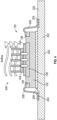
FIG. 4 shows an assembly that includes a flat pack no lead package that includes a heat exchanger connected to the flat pack no lead package. - A detailed description of one or more embodiments of the disclosed apparatus and method are presented herein by way of exemplification and not limitation with reference to the Figures.
- As noted above, in high density circuits/components such as QFNs and DFNs heat dissipation can become problematic. In particular, the fact that such components have a thermal pad (also known as a belly pad) on a same side of the component (e.g., same side of the component housing) as the metalized terminal pads of the component. In the prior art, the terminal pads and thermal belly pads were typically placed on or near the surface of substrate that is part of a printed circuit board (PCB). In this manner, vendors recommend, and it is industry accepted practice, to utilize the PCB to dissipate heat.
- To address the hot spots that such a configuration can lead to as disclosed above are systems (e.g., PCB's with flat no lead packages on them) where the flat no lead package is arranged such that the thermal belly pad and the terminal pads of the package are on the side of the package opposite the PCB. Optionally, a heat sink feature such as fin or a post can be thermally connected to the thermal belly pad to improve heat dissipation.
-
FIG. 1 shows an example of flat, nolead package 100. Thepackage 100 includes a body/housing 102. The body/housing 102 surrounds one or more circuits that are not shown but the skilled artisan will realize that all packages herein include one or more circuits therein. - The
housing 102 includes foursides 120a-120d inFIG. 1 and all four sides include one ormore openings 104 formed therein. Thus, as configured, thepackage 100 is a QFN. Of course, only two of sides (e.g., 120a and 120c) may include theopenings 104. In such a case, the package may be a DFN. Regardless, herein, thepackage 100 can include openings in 1, 2, 3 or 4 sides. Theopenings 104 are holes or slots that exposeterminal pads 106 so that electrical communication (e.g., power/data) can be conducted with the circuits inside thepackage 100. The terminal pads can be connected to a lead frame (not shown) as is known in the art. - As is common in QFNs/DFNs, the
package 100 can include a die that is surrounded by the lead frame. The lead frame is made up of a conductive material. The frame can be connected to the die by wire bonds. Theterminal pads 106 are electrically connected to the lead frame and allow the die to be electrically connected to a printed circuit board. As shown, thepackage 100 includes a first orbottom side 110 and a second ortop side 112. Thepackage 100 includes an exposedthermal belly pad 108 that passes at least thefirst side 110 and is exposed to an environment outside of thehousing 100. Thepad 108 can be an outer surface of thefirst side 110, level with it or slightly above it. Thispad 108 provides an efficient heat path from inside the package to outside the package. In the prior art, the pad was connected thermally to the PCB. - As noted above, in some cases, the heat from the
thermal belly pad 108 can create local hot spots on the PCB.FIG. 2 shows one example of how thepackage 100 can be arranged on aPCB 202 to form anassembly 200. The PCB 202 can include one ormore traces 204 formed thereon. Thetraces 204 can be formed of a conductive such as a metal (e.g., copper) and can be used to route electrical signals and power within and between devices connected to the PCB. ThePCB 202 can include asubstrate 203 that is formed of a rigid or flexible materials depending on the intended PCB design. Rigid materials can include but are not limited to FR4 or polyimide fiberglass, while flexible circuits and rigid-flex flexible layers typically use high-temperature polyimide films. Common plastic substrates for flexible circuits include polyimide (PI), liquid crystal polymer (LCP), polyester (PET), and polyethylene naphthalate (PEN) - The
substrate 203 as is known in the art provides a non-conductive base onto which thetraces 204 can be deposited. - In prior art applications, the
substrate 203 also served as material to absorb heat from thepackage 100. In such case, thebelly pad 108 was typically thermally connected (e.g., by way of thermal paste) to the PCB or to exposed copper trace(s) on the PCB to which the belly pad can be soldered. - In contrast, herein, the
assembly 200 can be formed by placing thesecond side 112 of the flat no-lead package 100 to afirst side 220 of thePCB 202. In this manner, the exposedthermal belly pad 108 is opposite thefirst side 220 of thePCB 202. This will prevent heat from thethermal belly pad 108 from being directly conducted into thePCB 202. Rather, as illustrated inFIG. 2 , heat from thethermal belly pad 108 can be discharged to anenvironment 240 outside of thehousing 102. - The
package 100 can be secured to the PCB 202 (and in one embodiment, to thefirst side 220 of the PCB 202) via an adhesive 208. - One or more metal leads 206 can connect various
terminal pads 106 totraces 204 on the board. The metal leads 206 can be wires or preformed and shaped leads, for example. - In one embodiment, the "environment" outside of the
housing 240 can be air. In another embodiment, the environment can be manifested as aheat transfer post 302 as shown inFIG. 3 . Theheat transfer post 302 can be connected to thebelly pad 108 by athermal interface material 304 such as a thermal paste. Theheat transfer post 302 can be connected to adevice housing 310 in which theassembly 100 is disposed. Thepost 302 can transfer heat in the manner shown by the arrows passing through it. - In another embodiment, and as shown in
FIG. 4 , a heat exchanger 402 (such as a finned heat exchanger) can be connected to thebelly pad 108 by athermal interface material 404 such as a thermal paste. This allows airflow to draw heat away. The other elements ofFIGs. 3 and4 are generally the same as inFIG. 2 . - Thus, disclosed are both assemblies and method of forming them that attach a flat no-lead package to a PCB in a manner that is exact opposite of the conventional manner. Such assemblies can reduce or avoid hot spots in the PCB in some embodiments.
- The term "about" is intended to include the degree of error associated with measurement of the particular quantity based upon the equipment available at the time of filing the application.
- The terminology used herein is for the purpose of describing particular embodiments only and is not intended to be limiting of the present disclosure. As used herein, the singular forms "a", "an" and "the" are intended to include the plural forms as well, unless the context clearly indicates otherwise. It will be further understood that the terms "comprises" and/or "comprising," when used in this specification, specify the presence of stated features, integers, steps, operations, elements, and/or components, but do not preclude the presence or addition of one or more other features, integers, steps, operations, element components, and/or groups thereof.
- While the present disclosure has been described with reference to an exemplary embodiment or embodiments, it will be understood by those skilled in the art that various changes may be made without departing from the scope of the invention as defined by the claims. In addition, many modifications may be made to adapt a particular situation or material to the teachings of the present disclosure without departing from the scope of the claims. Therefore, it is intended that the present disclosure not be limited to the particular embodiment disclosed as the best mode contemplated for carrying out this present disclosure, but that the present disclosure will include all embodiments falling within the scope of the claims.
Claims (15)
- A method of forming a circuit board assembly, the method comprising:receiving a flat no-lead package (100), wherein the package includes: a housing (102) having a first side (220) and second side; a circuit disposed within the housing; and an exposed thermal belly pad (108) that is thermally coupled to the circuit and passes at least partially through the first side such that it can be exposed to an environment outside of the housing; andattaching the second side of the flat no-lead package to a first side of a printed circuit board, PCB, (202) such that the exposed thermal belly pad is opposite the first side of the PCB.
- The method of claim 1, further comprising:
attaching a heat sink to the exposed thermal belly pad. - The method of claim 2, wherein the heat sink is a finned heat sink.
- The method of claim 2 or 3, wherein the heat sink is attached by a thermal paste.
- The method of any preceding claim, further comprising:
attaching a post (302) to the exposed thermal belly pad. - The method of claim 5, further comprising:putting the PCB in a housing; andthermally connecting the post to the housing.
- The method of claim 5, wherein the post is attached by a thermal paste.
- The method of any preceding claim, wherein the PCB includes traces (204) thereon and the method further comprises:
electrically connecting the flat no-lead package to the traces. - A circuit board assembly comprising:a flat no-lead package (100), wherein the package includes: a housing (102) having a first side (220) and second side; a circuit disposed within the housing; and an exposed thermal belly pad that is thermally coupled to the circuit and that passes at least partially through the first side; anda printed circuit board, PCB, (202) having traces (204) formed on a first side thereof, wherein the flat no-lead package is attached to a first side of the PCB such that the exposed thermal belly pad is opposite the first side of the PCB.
- The assembly of claim 9, further comprising:
a heat sink attached to the exposed thermal belly pad. - The assembly of claim 10, wherein the heat sink is a finned heat sink.
- The assembly of claim 10 or 11, wherein the heat sink is attached by a thermal paste.
- The assembly of any of claims 9 to 12, further comprising:
a post (302) attached to the exposed thermal belly pad. - The assembly of claim 13, further comprising:a housing surrounding the PCB; andwherein the post is thermally connected to the housing.
- The assembly of claim 13, wherein the post is attached by a thermal paste.
Applications Claiming Priority (1)
| Application Number | Priority Date | Filing Date | Title |
|---|---|---|---|
| US17/944,333 US20240090131A1 (en) | 2022-09-14 | 2022-09-14 | Thermal management for flat no lead packages |
Publications (1)
| Publication Number | Publication Date |
|---|---|
| EP4340554A1 true EP4340554A1 (en) | 2024-03-20 |
Family
ID=88017898
Family Applications (1)
| Application Number | Title | Priority Date | Filing Date |
|---|---|---|---|
| EP23196896.7A Pending EP4340554A1 (en) | 2022-09-14 | 2023-09-12 | Thermal management for flat no lead packages |
Country Status (2)
| Country | Link |
|---|---|
| US (1) | US20240090131A1 (en) |
| EP (1) | EP4340554A1 (en) |
Citations (5)
| Publication number | Priority date | Publication date | Assignee | Title |
|---|---|---|---|---|
| GB2197538A (en) * | 1986-10-24 | 1988-05-18 | Bicc Plc | Cooling module for use in a circuit board installation |
| US4821946A (en) * | 1987-02-19 | 1989-04-18 | Hitachi, Ltd. | Soldering method |
| US20010045644A1 (en) * | 2000-01-13 | 2001-11-29 | Chien-Ping Huang | Semiconductor package having heat sink at the outer surface |
| US20120020017A1 (en) * | 2010-07-20 | 2012-01-26 | Kehret William E | Printed circuit board module enclosure and apparatus using same |
| US20210143106A1 (en) * | 2019-11-11 | 2021-05-13 | Texas Instruments Incorporated | Packaged device carrier for thermal enhancement or signal redistribution of packaged semiconductor devices |
Family Cites Families (3)
| Publication number | Priority date | Publication date | Assignee | Title |
|---|---|---|---|---|
| US8283776B2 (en) * | 2010-01-26 | 2012-10-09 | Qualcomm Incorporated | Microfabricated pillar fins for thermal management |
| US8716859B2 (en) * | 2012-01-10 | 2014-05-06 | Intel Mobile Communications GmbH | Enhanced flip chip package |
| US11574853B2 (en) * | 2020-06-30 | 2023-02-07 | Taiwan Semiconductor Manufacturing Company, Ltd. | Semiconductor device |
-
2022
- 2022-09-14 US US17/944,333 patent/US20240090131A1/en active Pending
-
2023
- 2023-09-12 EP EP23196896.7A patent/EP4340554A1/en active Pending
Patent Citations (5)
| Publication number | Priority date | Publication date | Assignee | Title |
|---|---|---|---|---|
| GB2197538A (en) * | 1986-10-24 | 1988-05-18 | Bicc Plc | Cooling module for use in a circuit board installation |
| US4821946A (en) * | 1987-02-19 | 1989-04-18 | Hitachi, Ltd. | Soldering method |
| US20010045644A1 (en) * | 2000-01-13 | 2001-11-29 | Chien-Ping Huang | Semiconductor package having heat sink at the outer surface |
| US20120020017A1 (en) * | 2010-07-20 | 2012-01-26 | Kehret William E | Printed circuit board module enclosure and apparatus using same |
| US20210143106A1 (en) * | 2019-11-11 | 2021-05-13 | Texas Instruments Incorporated | Packaged device carrier for thermal enhancement or signal redistribution of packaged semiconductor devices |
Non-Patent Citations (1)
| Title |
|---|
| KELLY DANIEL: "Soldering QFN surface mount devices | Electronics Forums", MAKER PRO, 17 June 2004 (2004-06-17), pages 1 - 4, XP093125054, Retrieved from the Internet <URL:https://maker.pro/forums/threads/soldering-qfn-surface-mount-devices.13218/> [retrieved on 20240129] * |
Also Published As
| Publication number | Publication date |
|---|---|
| US20240090131A1 (en) | 2024-03-14 |
Similar Documents
| Publication | Publication Date | Title |
|---|---|---|
| US5157480A (en) | Semiconductor device having dual electrical contact sites | |
| US5773884A (en) | Electronic package with thermally conductive support member having a thin circuitized substrate and semiconductor device bonded thereto | |
| KR0169820B1 (en) | Chip scale package with metal wiring substrate | |
| EP0435093A2 (en) | Thin, molded, surface mount electronic device | |
| US9698132B1 (en) | Chip package stack up for heat dissipation | |
| JPH09283695A (en) | Semiconductor mounting structure | |
| GB2286084A (en) | Electronic package with thermally conductive support | |
| JPH033290A (en) | Thermal shunt for electronic circuit assembly and manufacture thereof | |
| TW448514B (en) | Semiconductor device and its manufacture, circuit board and electronic apparatus | |
| US5949651A (en) | Quad flat pack integrated circuit package | |
| US5548087A (en) | Molded plastic packaging of electronic devices | |
| US6552907B1 (en) | BGA heat ball plate spreader, BGA to PCB plate interface | |
| JPH10335374A (en) | Semiconductor device and semiconductor device module | |
| CN106717135B (en) | PCB and PCB Layout | |
| JP2003188565A (en) | Heat dissipation structure of surface mount electronic component | |
| EP0164794A2 (en) | Multi-layer heat sinking integrated circuit package | |
| US20240090131A1 (en) | Thermal management for flat no lead packages | |
| JP2801810B2 (en) | Resin-sealed semiconductor device | |
| US8053285B2 (en) | Thermally enhanced single inline package (SIP) | |
| JPH03174749A (en) | Semiconductor device | |
| JPH05315782A (en) | Heat dissipating structure of printed circuit board | |
| JP3630713B2 (en) | Surface mounting package and package mounting apparatus | |
| CN111554651A (en) | Surface mount semiconductor device and method of manufacturing the same | |
| JPH03238852A (en) | Mold type semiconductor integrated circuit | |
| CN216013569U (en) | LED test board and test device |
Legal Events
| Date | Code | Title | Description |
|---|---|---|---|
| PUAI | Public reference made under article 153(3) epc to a published international application that has entered the european phase |
Free format text: ORIGINAL CODE: 0009012 |
|
| STAA | Information on the status of an ep patent application or granted ep patent |
Free format text: STATUS: THE APPLICATION HAS BEEN PUBLISHED |
|
| AK | Designated contracting states |
Kind code of ref document: A1 Designated state(s): AL AT BE BG CH CY CZ DE DK EE ES FI FR GB GR HR HU IE IS IT LI LT LU LV MC ME MK MT NL NO PL PT RO RS SE SI SK SM TR |
|
| STAA | Information on the status of an ep patent application or granted ep patent |
Free format text: STATUS: REQUEST FOR EXAMINATION WAS MADE |
|
| 17P | Request for examination filed |
Effective date: 20240919 |
|
| RBV | Designated contracting states (corrected) |
Designated state(s): AL AT BE BG CH CY CZ DE DK EE ES FI FR GB GR HR HU IE IS IT LI LT LU LV MC ME MK MT NL NO PL PT RO RS SE SI SK SM TR |