EP4340468A1 - Vorrichtungen und verfahren zur rauschminderung - Google Patents
Vorrichtungen und verfahren zur rauschminderung Download PDFInfo
- Publication number
- EP4340468A1 EP4340468A1 EP23196739.9A EP23196739A EP4340468A1 EP 4340468 A1 EP4340468 A1 EP 4340468A1 EP 23196739 A EP23196739 A EP 23196739A EP 4340468 A1 EP4340468 A1 EP 4340468A1
- Authority
- EP
- European Patent Office
- Prior art keywords
- electronic device
- noise
- transmission power
- signal
- indication
- Prior art date
- Legal status (The legal status is an assumption and is not a legal conclusion. Google has not performed a legal analysis and makes no representation as to the accuracy of the status listed.)
- Pending
Links
Images




Classifications
-
- H—ELECTRICITY
- H04—ELECTRIC COMMUNICATION TECHNIQUE
- H04B—TRANSMISSION
- H04B1/00—Details of transmission systems, not covered by a single one of groups H04B3/00 - H04B13/00; Details of transmission systems not characterised by the medium used for transmission
- H04B1/02—Transmitters
- H04B1/04—Circuits
- H04B1/0475—Circuits with means for limiting noise, interference or distortion
-
- H—ELECTRICITY
- H04—ELECTRIC COMMUNICATION TECHNIQUE
- H04W—WIRELESS COMMUNICATION NETWORKS
- H04W52/00—Power management, e.g. Transmission Power Control [TPC] or power classes
- H04W52/04—Transmission power control [TPC]
- H04W52/18—TPC being performed according to specific parameters
- H04W52/24—TPC being performed according to specific parameters using SIR [Signal to Interference Ratio] or other wireless path parameters
- H04W52/243—TPC being performed according to specific parameters using SIR [Signal to Interference Ratio] or other wireless path parameters taking into account interferences
-
- H—ELECTRICITY
- H04—ELECTRIC COMMUNICATION TECHNIQUE
- H04B—TRANSMISSION
- H04B1/00—Details of transmission systems, not covered by a single one of groups H04B3/00 - H04B13/00; Details of transmission systems not characterised by the medium used for transmission
- H04B1/005—Details of transmission systems, not covered by a single one of groups H04B3/00 - H04B13/00; Details of transmission systems not characterised by the medium used for transmission adapting radio receivers, transmitters andtransceivers for operation on two or more bands, i.e. frequency ranges
- H04B1/0053—Details of transmission systems, not covered by a single one of groups H04B3/00 - H04B13/00; Details of transmission systems not characterised by the medium used for transmission adapting radio receivers, transmitters andtransceivers for operation on two or more bands, i.e. frequency ranges with common antenna for more than one band
-
- H—ELECTRICITY
- H04—ELECTRIC COMMUNICATION TECHNIQUE
- H04B—TRANSMISSION
- H04B1/00—Details of transmission systems, not covered by a single one of groups H04B3/00 - H04B13/00; Details of transmission systems not characterised by the medium used for transmission
- H04B1/38—Transceivers, i.e. devices in which transmitter and receiver form a structural unit and in which at least one part is used for functions of transmitting and receiving
- H04B1/3827—Portable transceivers
- H04B1/3833—Hand-held transceivers
- H04B1/3838—Arrangements for reducing RF exposure to the user, e.g. by changing the shape of the transceiver while in use
-
- H—ELECTRICITY
- H04—ELECTRIC COMMUNICATION TECHNIQUE
- H04M—TELEPHONIC COMMUNICATION
- H04M1/00—Substation equipment, e.g. for use by subscribers
- H04M1/72—Mobile telephones; Cordless telephones, i.e. devices for establishing wireless links to base stations without route selection
- H04M1/724—User interfaces specially adapted for cordless or mobile telephones
- H04M1/72448—User interfaces specially adapted for cordless or mobile telephones with means for adapting the functionality of the device according to specific conditions
- H04M1/72454—User interfaces specially adapted for cordless or mobile telephones with means for adapting the functionality of the device according to specific conditions according to context-related or environment-related conditions
-
- H—ELECTRICITY
- H04—ELECTRIC COMMUNICATION TECHNIQUE
- H04M—TELEPHONIC COMMUNICATION
- H04M2250/00—Details of telephonic subscriber devices
- H04M2250/52—Details of telephonic subscriber devices including functional features of a camera
Definitions
- the present disclosure relates generally to improving signal quality, and more specifically to reducing noise in signals.
- the signals may couple to a sensor.
- the signals may manifest noise at the sensor, and thus be captured as noise by the sensor.
- the sensor may include a camera sensor, and a transmission signal may be captured as row noise in an image captured by the camera sensor.
- an electronic device includes an antenna, a transmitter coupled to the antenna that transmits a radio frequency signal via the antenna, a camera that captures an image, and processing circuitry coupled to the transmitter and the camera.
- the processing circuitry reduces transmission power to the transmitter based on the camera capturing the image.
- a method in another embodiment, includes receiving, at processing circuitry of an electronic device, an indication that a sensor of the electronic device is being used, and reducing the transmission power based on the indication.
- one or more tangible, non-transitory, computer-readable media stores instructions that cause one or more processors to receive a first indication that a sensor is being used for facial identification, receive a second indication that a transmitter is transmitting a signal at a transmission power, and reduce the transmission power based on the first indication and the second indication.
- any exact values, numbers, measurements, and so on, provided herein, are contemplated to include approximations (e.g., within a margin of suitable or contemplatable error) of the exact values, numbers, measurements, and so on.
- the term "set" may include one or more. That is, a set may include a unitary set of one member, but the set may also include a set of multiple members.
- the signals may couple to a sensor.
- the signals may manifest noise at the sensor, and thus be captured as noise by the sensor.
- the sensor may include a camera sensor, and a transmission signal may be captured as row noise in an image captured by the camera sensor.
- Embodiments herein provide various apparatuses and techniques to improve signal quality (e.g., for signals captured by the sensor) by reducing noise.
- the noise may be caused by transmission signals having frequencies in certain frequency bands
- noise in the sensor signals may be reduced by reducing power of the transmission signals (e.g., reducing power to a transmitter transmitting the signals).
- the embodiments disclosed herein may determine when the sensor (e.g., the camera sensor) is being used, determine if the transmitter is transmitting a signal, determine whether the signal has a frequency in the certain frequency bands (e.g., that cause noise at the sensor), and reduce power (e.g., perform a power back-off operation) at the transmitter if so. In this way, the disclosed embodiments may reduce noise at the sensor.
- the embodiments may also or alternatively be applied to other victims of noise (e.g., other sensors, components, or devices) and other sources of noise (e.g., operation of other components or devices).
- victims of noise e.g., other sensors, components, or devices
- sources of noise e.g., operation of other components or devices
- FIG. 1 is a block diagram of an electronic device 10, according to embodiments of the present disclosure.
- the electronic device 10 may include, among other things, one or more processors 12 (collectively referred to herein as a single processor for convenience, which may be implemented in any suitable form of processing circuitry), memory 14, nonvolatile storage 16, a display 18, input structures 22, an input/output (I/O) interface 24, a network interface 26, and a power source 29.
- the various functional blocks shown in FIG. 1 may include hardware elements (including circuitry), software elements (including machine-executable instructions) or a combination of both hardware and software elements (which may be referred to as logic).
- the processor 12, memory 14, the nonvolatile storage 16, the display 18, the input structures 22, the input/output (I/O) interface 24, the network interface 26, and/or the power source 29 may each be communicatively coupled directly or indirectly (e.g., through or via another component, a communication bus, a network) to one another to transmit and/or receive signals between one another.
- FIG. 1 is merely one example of a particular implementation and is intended to illustrate the types of components that may be present in the electronic device 10.
- the electronic device 10 may include any suitable computing device, including a desktop or notebook computer (e.g., in the form of a MacBook ® , MacBook ® Pro, MacBook Air ® , iMac ® , Mac ® mini, or Mac Pro ® available from Apple Inc. of Cupertino, California), a portable electronic or handheld electronic device such as a wireless electronic device or smartphone (e.g., in the form of a model of an iPhone ® available from Apple Inc. of Cupertino, California), a tablet (e.g., in the form of a model of an iPad ® available from Apple Inc. of Cupertino, California), a wearable electronic device (e.g., in the form of an Apple Watch ® by Apple Inc.
- a desktop or notebook computer e.g., in the form of a MacBook ® , MacBook ® Pro, MacBook Air ® , iMac ® , Mac ® mini, or Mac Pro ® available from Apple Inc. of Cupertino, California
- processor 12 and other related items in FIG. 1 may be embodied wholly or in part as software, hardware, or both. Furthermore, the processor 12 and other related items in FIG. 1 may be a single contained processing module or may be incorporated wholly or partially within any of the other elements within the electronic device 10.
- the processor 12 may be implemented with any combination of general-purpose microprocessors, microcontrollers, digital signal processors (DSPs), field programmable gate array (FPGAs), programmable logic devices (PLDs), controllers, state machines, gated logic, discrete hardware components, dedicated hardware finite state machines, or any other suitable entities that may perform calculations or other manipulations of information.
- the processors 12 may include one or more application processors, one or more baseband processors, or both, and perform the various functions described herein.
- the processor 12 may be operably coupled with a memory 14 and a nonvolatile storage 16 to perform various algorithms.
- Such programs or instructions executed by the processor 12 may be stored in any suitable article of manufacture that includes one or more tangible, computer-readable media.
- the tangible, computer-readable media may include the memory 14 and/or the nonvolatile storage 16, individually or collectively, to store the instructions or routines.
- the memory 14 and the nonvolatile storage 16 may include any suitable articles of manufacture for storing data and executable instructions, such as random-access memory, read-only memory, rewritable flash memory, hard drives, and optical discs.
- programs e.g., an operating system
- encoded on such a computer program product may also include instructions that may be executed by the processor 12 to enable the electronic device 10 to provide various functionalities.
- the display 18 may facilitate users to view images generated on the electronic device 10.
- the display 18 may include a touch screen, which may facilitate user interaction with a user interface of the electronic device 10.
- the display 18 may include one or more liquid crystal displays (LCDs), light-emitting diode (LED) displays, organic light-emitting diode (OLED) displays, active-matrix organic light-emitting diode (AMOLED) displays, or some combination of these and/or other display technologies.
- LCDs liquid crystal displays
- LED light-emitting diode
- OLED organic light-emitting diode
- AMOLED active-matrix organic light-emitting diode
- the input structures 22 of the electronic device 10 may enable a user to interact with the electronic device 10 (e.g., pressing a button to increase or decrease a volume level).
- the I/O interface 24 may enable electronic device 10 to interface with various other electronic devices, as may the network interface 26.
- the I/O interface 24 may include an I/O port for a hardwired connection for charging and/or content manipulation using a standard connector and protocol, such as the Lightning connector provided by Apple Inc. of Cupertino, California, a universal serial bus (USB), or other similar connector and protocol.
- the network interface 26 may include, for example, one or more interfaces for a personal area network (PAN), such as an ultra-wideband (UWB) or a BLUETOOTH ® network, a local area network (LAN) or wireless local area network (WLAN), such as a network employing one of the IEEE 802.11x family of protocols (e.g., WI-FI ® ), and/or a wide area network (WAN), such as any standards related to the Third Generation Partnership Project (3GPP), including, for example, a 3 rd generation (3G) cellular network, universal mobile telecommunication system (UMTS), 4 th generation (4G) cellular network, long term evolution (LTE ® ) cellular network, long term evolution license assisted access (LTE-LAA) cellular network, 5 th generation (5G) cellular network, and/or New Radio (NR) cellular network, a 6 th generation (6G) or greater than 6G cellular network, a satellite network, a non-terrestrial network, and so on.
- the network interface 26 may include, for example, one or more interfaces for using a cellular communication standard of the 5G specifications that include the millimeter wave (mmWave) frequency range (e.g., 24.25-300 gigahertz (GHz)) that defines and/or enables frequency ranges used for wireless communication.
- the network interface 26 of the electronic device 10 may allow communication over the aforementioned networks (e.g., 5G, Wi-Fi, LTE-LAA, and so forth).
- the network interface 26 may also include one or more interfaces for, for example, broadband fixed wireless access networks (e.g., WIMAX ® ), mobile broadband Wireless networks (mobile WIMAX ® ), asynchronous digital subscriber lines (e.g., ADSL, VDSL), digital video broadcasting-terrestrial (DVB-T ® ) network and its extension DVB Handheld (DVB-H ® ) network, ultra-wideband (UWB) network, alternating current (AC) power lines, and so forth.
- broadband fixed wireless access networks e.g., WIMAX ®
- mobile broadband Wireless networks e.g., mobile broadband Wireless networks (mobile WIMAX ® )
- asynchronous digital subscriber lines e.g., ADSL, VDSL
- DVD-T ® digital video broadcasting-terrestrial
- DVD-H ® extension DVB Handheld
- UWB ultra-wideband
- AC alternating current
- the network interface 26 may include a transceiver 30.
- the transceiver 30 may support transmission and receipt of various wireless signals via one or more antennas, and thus may include a transmitter and a receiver.
- the power source 29 of the electronic device 10 may include any suitable source of power, such as a rechargeable lithium polymer (Li-poly) battery and/or an alternating current (AC) power converter.
- FIG. 2 is a functional diagram of the electronic device 10 of FIG. 1 , according to embodiments of the present disclosure.
- the processor 12, the memory 14, the transceiver 30, a transmitter 52, a receiver 54, and/or antennas 55 may be communicatively coupled directly or indirectly (e.g., through or via another component, a communication bus, a network) to one another to transmit and/or receive signals between one another.
- the electronic device 10 may include the transmitter 52 and/or the receiver 54 that respectively enable transmission and reception of signals between the electronic device 10 and an external device via, for example, a network (e.g., including base stations or access points) or a direct connection. As illustrated, the transmitter 52 and the receiver 54 may be combined into the transceiver 30.
- the electronic device 10 may also have one or more antennas 55A-55N electrically coupled to the transceiver 30.
- the antennas 55A-55N may be configured in an omnidirectional or directional configuration, in a single-beam, dual-beam, or multi-beam arrangement, and so on. Each antenna 55 may be associated with one or more beams and various configurations.
- multiple antennas of the antennas 55A-55N of an antenna group or module may be communicatively coupled to a respective transceiver 30 and each emit radio frequency signals that may constructively and/or destructively combine to form a beam.
- the electronic device 10 may include multiple transmitters, multiple receivers, multiple transceivers, and/or multiple antennas as suitable for various communication standards.
- the transmitter 52 and the receiver 54 may transmit and receive information via other wired or wireline systems or means.
- the electronic device 10 may also include one or more cameras or image or light sensors (e.g., as part of the input structures 22).
- the one or more cameras or image or light sensors may capture images or determine amounts of light (e.g., visible light, infrared light, ultraviolet light, and so on) surrounding the electronic device 10.
- the camera 56 may include a front-facing camera (e.g., disposed on a display surface of the electronic device 10 having the display 18) and/or a rear-facing camera (e.g., disposed on a base or back surface, opposite the display surface, of the electronic device 10).
- the camera 56 may include any other suitable sensor that may be affected by noise caused by operation of an aggressor device or component (e.g., the transmitter 52).
- the electronic device 10 may include facial identification (ID) circuitry 58 that receives one or more images captured by the camera 56, and determines whether the one or more images matches, corresponds to, or correlates to a face (e.g., in a database of faces).
- the facial ID circuitry 58 may perform facial identification or recognition for authentication or security purposes, such as to unlock the electronic device 10 for a user.
- the facial ID circuitry 58 may include hardware elements, software elements, or both.
- the facial ID circuitry 58 may be, at least in part, part of or coupled to the processor 12, include instructions or code stored in the memory 14 and/or the storage 16, and so on.
- the various components of the electronic device 10 may be coupled together by a bus system 59.
- the bus system 59 may include a data bus, for example, as well as a power bus, a control signal bus, and a status signal bus, in addition to the data bus.
- the components of the electronic device 10 may be coupled together or accept or provide inputs to each other using some other mechanism.
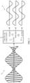
- FIG. 3 is a schematic diagram illustrating a modulated signal 70 emitted from an antenna 55 of the electronic device 10 coupling to the facial ID circuitry 58 of FIG. 2 at a ground connection 72 (e.g., an analog ground connection (AGND)).
- a ground connection 72 e.g., an analog ground connection (AGND)
- the modulated signal 70 may be generated by adding data to be transmitted to a carrier signal.
- the modulated signal 70 may include a low frequency signal that results in low frequency noise 74 at an output by the facial ID circuitry 58. This may be because the camera 56 is sensitive to the low frequency noise 74.
- the noise 74 may be exhibited in one or more voltage supplies of the facial ID circuitry 58, such as a digital voltage supply (DVDD) 76A, a digital input/output voltage supply (DOVDD) 76B, an analog voltage supply (AVDD) 76C, and so on.
- DVDD digital voltage supply
- DOVDD digital input/output voltage supply
- AVDD analog voltage supply
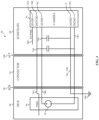
- FIG. 4 is a schematic diagram illustrating how the noise 74 is injected into the camera 56 of the electronic device 10 from the facial ID circuitry 58.
- the facial ID circuitry 58 includes a main logic board (MLB) 90, a connector 92, and a substrate 94.
- the MLB 90 may include, among other things, processing circuitry (which may be part of or coupled to the processor 12), memory (which may be part of or coupled to the memory 14), controller circuitry that controls or operates the facial ID circuitry 58, and, as illustrated, a power management unit (PMU) or power management circuitry 96, that manages power usage in the facial ID circuitry 58.
- the PMU 96 may include a power source 29, which may supply power to the facial ID circuitry 58.
- the PMU 96 may be electrically coupled to the connector 92 via an interface, such a board-to-board (B2B) interface 98.
- the connector 92 may include any suitable device or component that electrically couples the PMU 96 to the substrate 94.
- the connector 92 may be flexible to enable chip-to-chip (e.g., semiconductor die-to-semiconductor die) routing, including a flat flexible cable, flexible printed circuit, and so on.
- the connector 92 may be electrically coupled to the substrate 94 via an interface, such as an anisotropic conductive film (ACF) 100.
- the ACF 100 may include an adhesive interconnect system used to make electrical and/or mechanical connections between the connector 92 and the substrate 94.
- the substrate 94 may be part of a printed circuit board, to which the camera 56 is mounted or otherwise affixed. It should be understood that the connecting components, including the B2B interface 98, the connector 92, and/or the ACF 100 may include any suitable component or components that enable electrically coupling the PMU 96 to the substrate 94, as illustrated in FIG. 4 .
- the PMU 96 may provide the DOVDD 76B, the AVDD 76C, the AGND 72, and a ground connection (e.g., a digital ground connection (DGND)) 102 to the substrate 94 via the B2B interface 98, the connector 92, and the ACF 100.
- the MLB 90 may provide the DOVDD 76B from a power supply external to the MLB 90, and provide the AGND 72 from a ground 104 external to the MLB 90.
- the MLB 90 may additionally or alternatively provide the AVDD 76C and/or the DGND 102 via an internal power source 29.
- the substrate 94 may also provide the DVDD 76A to the PMU 96.
- the transmitter 52 transmits wireless signals 70 on certain radio frequency bands (such as LTE frequency bands, sub-6G frequency bands (e.g., less than 95 gigahertz (GHz) to 3 terahertz (THz) frequencies, sub-THz frequencies, and so on) or certain types of wireless signals 70 via the antenna 55
- the signals 70 may couple to the camera 56.
- the signals 70 may manifest noise at the camera 56, and thus be captured as noise 74 by the camera 56.
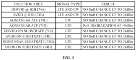
- FIG. 5 is a table of noise injection areas and results.
- noise 74A of an LTE signal e.g., a wireless signal that between 400 MHz and 6000 MHz, between 400 MHz and 2200 MHz, and so on
- CW continuous waveform
- An LTE signal may include a modulated signal (e.g., modulated via orthogonal frequency-division multiplexing (OFDM) having a frequency between 400 MHz and 6000 MHz, between 400 MHz and 2200 MHz, and so on. Because the LTE signal is modulated using, for example, OFDM, the LTE signal may not be characterized as continuous, as it does not have a constant amplitude or frequency throughout the signal. On the other hand, a CW signal may include an electromagnetic wave having a constant amplitude or frequency (such as a sine wave).
- OFDM orthogonal frequency-division multiplexing
- the noise 74D may result degrade or decrease RnR when the transmission power of the signal 70 is greater than 9 dBm. This may be because an electrostatic diode (ESD) structure on the ground connection 72 may rectify modulation (e.g., LTE modulation) of the transmitted signal 70 and fold or decrease it to or near 0 hertz (Hz), which may affect operation of the camera 56.
- ESD electrostatic diode
- FIG. 6 is a schematic diagram of how the noise 74 is injected into the camera 56 of the electronic device 10.
- the signal 70 e.g., a GHz-signal
- the modulated radio frequency signal 70 may couple into flex traces 132 of or coupled to the camera 56 (e.g., of the connector 92 in FIG. 5 ).
- the ESD structure 134 coupled to or of the ground connection 72 may rectify 136 and/or fold the GHz-signal 70 to sensor-susceptible frequencies (e.g., near or at 0 Hz), causing RnR degradation 138 at the camera 56.
- the camera 56 receives the noise 74 in a captured, received, or sensed signal (e.g., used for facial identification).
- the ESD structure 134 may include one or more diodes used to absorb abnormal voltages and/or static electricity discharge to protect components of the electronic device 10.
- the noise 74 may manifest as row or horizontally-lined artifacts in images captured by the camera 56, referred to as "row noise.”
- FIG. 7 illustrates unstructured pixel noise 150 that results in little to no row noise in a resulting image 152, and structured noise 74 from a transmitted signal 70 that, when combined with the unstructured pixel noise 150, results in row noise 154 in a resulting image 156.
- the image 152 captured by the camera 56 resulting from the unstructured pixel noise 150 is of good quality (e.g., there are no artifacts or errors due to noise).
- the image 152 captured by the camera 56 resulting from the unstructured pixel noise 150 may have a high RnR score.
- a combination 158 of the unstructured pixel noise 150 and the structured noise 74 may result in the image 156 captured by the camera 56 showing the row noise 154.
- the combination 158 of the unstructured pixel noise 150 and the structured noise 74 may have a low RnR score.
- RnR may be defined as a ratio of unstructured vs. spatially structured noise in a numerical three-dimensional array, and may be an imaging metric formed by human psycho-visual analysis.
- the combination 158 of the unstructured pixel noise 150 and the structured noise 74 may lead to failures to unlock the electronic device 10, which may lead to a negative or unacceptable user experience.
- While certain hardware mitigations may be implemented, such as a spring to a mid-chassis ground connection, a merged flex cable, foam on top of the facial ID circuitry 58, and so on, such mitigations may only help for some frequency bands, but not all that affect the camera 56. Instead, software or processor-controlled mitigation may be more effective to address the noise 74 for more or all frequency bands. In particular, the software or processor-controlled mitigation techniques may decrease transmission power (perform a power back-off procedure at the transmitter 52) or deactivate the antenna 55 (e.g., that is the aggressor, that creates the noise 74 at the camera 56).
- the processor 12 may decrease or back-off the transmission power by a predetermined amount, such as less than 2 decibels (dB), 2 dB or more, 3 dB or more, between 2 dB and 3 dB (e.g., apply a -2 dB or -3 dB power back-off), and so on, when the camera 56 is being used (e.g., for facial identification purposes).
- the processor 12 may decrease or back-off the transmission power by the predetermined amount for a predetermined time period (e.g., a duration that facial identification may be performed, such as 10 seconds or less, 5 seconds or less, 1 second or less, 0.5 seconds or less, and so on, such as 0.8 seconds).
- the processor 12 may decrease or back-off the transmission power when it determines that the transmitter 52 is transmitting signals of a frequency that causes the noise 74 at the camera 56.
- the memory 14 and/or the storage 16 may store a data structure (e.g., a table, a list, and so on) that includes identifiers of frequency bands that, for signals having frequencies in those bands, cause the noise 74 at the camera 56.
- FIG. 8 is an example table 170 of frequency bands that, for signals having frequencies in those bands, cause the noise 74 at the camera 56. In some embodiments, these frequency bands may be determined at a testing, manufacturing, or production stage or facility of the electronic device 10.
- the processor 12 may cause the transmitter 52 to iterate through transmitting signals having different frequencies, and determine whether those frequencies result in row noise 154 in a victim software application or circuitry, such as when performing facial identification. If so, those frequencies or frequency bands having those frequencies may be stored in the memory 14 and/or the storage 16.
- the table 170 lists, in a first row, frequency bands B11 (a frequency division duplex (FDD) LTE 1500 MHz frequency band having an uplink frequency range of 1427.9-1452.9 MHz and a downlink frequency range of 1475.9-1500.9 MHz), B21 (an FDD LTE 1500 MHz frequency band having an uplink frequency range of 1447.9-1462.9 MHz and a downlink frequency range of 1495.9-1510.9 MHz), B25 (an FDD LTE 1900 MHz frequency band having an uplink frequency range of 1850-1915 MHz and a downlink frequency range of 1930-1995 MHz), B39 (a time division duplex (TDD) LTE 1900 MHz frequency band having an operating frequency range of 1880-1920 MHz), and B66 (an FDD LTE 1700 MHz frequency band having an uplink frequency range of 1710-1780 MHz and a downlink frequency range of 2110-2200 MHz).
- FDD frequency division duplex
- the table 170 also lists, in a second row, frequency bands B1 (an FDD LTE 2100 MHz frequency band having an uplink frequency range of 1920-1980 MHz and a downlink frequency range of 2110-2170 MHz), B2 (an FDD LTE 1900 MHz frequency band having an uplink frequency range of 1850-1910 MHz and a downlink frequency range of 1930-1990 MHz), B3 (an FDD LTE 1800 MHz frequency band having an uplink frequency range of 1710-1785 MHz and a downlink frequency range of 1805-1880 MHz), B40 (a TDD LTE 2300 MHz frequency band having an operating frequency range of 2300-2400 MHz), and B41 (a TDD LTE 2500 MHz frequency band having an operating frequency range of 2496-2690 MHz).
- the table 170 further lists, in a third row, frequency band 5G sub-6 GHz (Frequency Range 1) N77 (a TDD 5G NR 3700 MHz frequency band having an operating frequency range of 3300-4200 MHz).
- the processor 12 may decrease or back-off the transmission power when it determines that the transmitter 52 is transmitting signals of a frequency within a frequency band listed in the table 170 (which may result in producing the noise 74 at the camera 56).
- an algorithm or machine-learning technique may be used to determine the frequency bands that, for signals having frequencies in those bands, cause the noise 74 at the camera 56. It should be understood that the frequency bands in the table are merely examples, and that, in additional or alternative embodiments, different frequency bands and/or ranges may be included, and certain listed frequency bands may be removed.
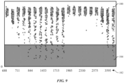
- FIG. 9 is a frequency diagram illustrating RnR scores 180 over frequencies 182 from 688 MHz to 4 GHz.
- Signals 70 having frequencies that fall within a low RnR score region 184 may include noise 74 that causes the row noise 154 in a victim software application or circuitry, such as when executing a facial identification software application or the facial ID circuitry 58.
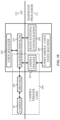
- FIG. 10 is a software block diagram of software executing on the electronic device 10 (e.g., stored in the memory 14 and executed by the processor 12) that performs noise mitigation, according to embodiments of the present disclosure.
- a UWB/Camera Coexistence State Machine 200 may enable or disable antenna 55 blocking (e.g., deactivation) and/or perform a power back-off of the transmitter 52 based on receiving an indication of a camera trigger 202 from the camera 56 of the facial ID circuitry 58.
- the indication of the camera trigger 202 may correspond or correlate to the activation of the camera trigger 202 (e.g., by a user, a software application executing on the electronic device 10, and so on), such as if a facial ID software application is open and/or executing.
- the indication of the camera trigger 202 may be received and/or managed by camera trigger logic 204, which may be implemented in software, hardware, or both.
- the camera trigger logic 204 may include the camera 56, device drivers 206 enabling the processor 12 to interface with the camera 56, and baseband services 207.
- the baseband services 207 may include software that enables the processor 12 (e.g., a baseband processor) to manage radio functions, including those performed by the transceiver 30, the transmitter 52, and/or the receiver 54.
- the baseband services 207 may enable the processor 12 to interface with the camera 56 via the drivers 206, receive an indication of the camera trigger 202 (e.g., activation of the camera 56), and/or configure 208 frequency bands and/or the antenna 55.
- the baseband services 207 may enable the processor 12 to configure the transmitter 52, the receiver 54, and/or the antenna 55 to transmit or receive signals having target frequencies.
- the top half of the software components including the camera 56, the drivers 206, the baseband services 207, and a Coexistence Manager 209 that may configure the antenna 55 for the camera 56 may be executed by or part of an application processor 210 (which may be included as part of the processing circuitry 12), and the bottom half 190 of the software components, including the indication of the camera trigger 202, the UWB/Camera Coexistence State Machine 200, and the band/antenna configuration 208 may be executed by or part of a baseband processor 211 (which may also be included as part of the processing circuitry 12).
- an application processor 210 which may be included as part of the processing circuitry 12
- the bottom half 190 of the software components including the indication of the camera trigger 202, the UWB/Camera Coexistence State Machine 200, and the band/antenna configuration 208 may be executed by or part of a baseband processor 211 (which may also be included as part of the processing circuitry 12).
- FIG. 11 is a flowchart of a method 212 for reducing noise cause by signal transmission when performing facial identification (or operating any other suitable victim software application or circuitry), according to embodiments of the present disclosure.
- Any suitable device e.g., a controller
- the method 212 may be implemented by executing instructions stored in a tangible, non-transitory, computer-readable medium, such as the memory 14 or storage 16, using the processor 12.
- the method 212 may be performed at least in part by one or more of the software components shown in FIG.
- the processor 12 receives an indication of usage of the camera 56 of the facial ID circuitry 58 (or any other suitable indication of usage associated with another victim software application or circuitry). For example, the processor 12 may receive an indication that the camera 56 is being used for facial identification, such as by receiving an indication of the camera trigger 202, execution of a facial ID software application, and so on.
- the processor 12 determines if the transmitter 52 is in use or if an indication that the electronic device 10 is transmitting a radio frequency signal (e.g., 70) is received. In some embodiments, the processor 12 may determine if the transmitter 52 is transmitting the signal 70 using an antenna 55 that is within a threshold proximity of the camera 56 (e.g., such that the signal 70 may inject the noise 74 into a ground connection 72 of the camera 56). If not, the processor 12 returns to process block 214.
- a radio frequency signal e.g. 70
- the processor 12 determines whether power back-off should be performed for a current band/antenna configuration.
- the processor 12 may receive or determine a frequency of the signal 70 being transmitted by the transmitter 52, and receive an indication of or determine whether the frequency of the signal 70 may cause the noise 74 at the camera 56.
- the memory 14 and/or the storage 16 may store a data structure (e.g., a table, a list, and so on) listing frequency bands and/or antenna configurations for which, for signals having frequencies in those frequency bands and/or associate with those antenna configurations, cause the noise 74 at the camera 56.
- a data structure e.g., a table, a list, and so on
- FIG. 8 is an example of such a data structure. While the example of FIG. 8 only shows frequency bands or ranges for which to perform a power back-off, the table 170 may be for a single antenna 55 or set of antennas 55, and another antenna 55 or set of antennas 55 may correspond to another table.
- the processor 12 may select a table based on the antenna 55 or antennas 55 that are transmitting the signal 70, and then determine whether the frequency band of that signal 70 is listed in the selected table. In any case, the processor 12 may determine whether the frequency of the signal 70 is within or correlates to a frequency band listed in the table (e.g., the processor 12 may compare the frequency of the signal 70 with frequency bands listed in the table).
- the processor 12 does not perform a power back-off (e.g., may maintain transmission power of the transmitter 52), and returns to process block 214. However, if the frequency of the signal 70 is within or does correlate to a frequency band listed in the table, then in process block 220, the processor 12 causes the transmitter 52 to perform a power back-off (e.g., reduce the transmission power to the transmitter 52).
- the data structure or table 170 may include a power back-off amount (e.g., in dB) for which to perform the power back-off. For example, though not shown in the example table of FIG.
- each frequency band listed in the table may be associated with a back-off amount (e.g., -2 dB, -3 dB, and so on).
- the processor 12 causes the transmitter 52 to reduce its power by the amount corresponding to the frequency band associated with the transmission signal 70.
- the processor 12 may deactivate the transmitter 52, to cause the transmitter power to back-off to 0 dBm.
- the processor 12 may wait before causing the transmitter 52 to return to its previous transmission power.
- a duration for the wait may be any suitable time period, though, in some embodiments, may correspond to operation of the camera 56 and/or the victim software application or circuitry.
- the victim circuitry may include the facial ID circuitry 58.
- a threshold duration corresponding to perform facial identification may be 0.8 seconds or less, 1 second or less, 2 seconds or less, and so on.
- the processor 12 may wait the threshold duration.
- the processor 12 in process block 224, causes the transmitter 52 to increase its transmission power (e.g., back to its previous transmission power before it applied the power back-off). In this manner, the method 212 may reduce noise cause by signal transmission when performing facial identification (or operating any other suitable victim software application or circuitry), resulting in less row noise in facial identification images, and a better user experience.
- personally identifiable information should follow privacy policies and practices that are generally recognized as meeting or exceeding industry or governmental requirements for maintaining the privacy of users.
- personally identifiable information data should be managed and handled so as to minimize risks of unintentional or unauthorized access or use, and the nature of authorized use should be clearly indicated to users.
Landscapes
- Engineering & Computer Science (AREA)
- Computer Networks & Wireless Communication (AREA)
- Signal Processing (AREA)
- Environmental & Geological Engineering (AREA)
- Human Computer Interaction (AREA)
- Studio Devices (AREA)
Applications Claiming Priority (2)
| Application Number | Priority Date | Filing Date | Title |
|---|---|---|---|
| US202263407016P | 2022-09-15 | 2022-09-15 | |
| US18/079,531 US20240097723A1 (en) | 2022-09-15 | 2022-12-12 | Apparatuses and methods for noise mitigation |
Publications (1)
| Publication Number | Publication Date |
|---|---|
| EP4340468A1 true EP4340468A1 (de) | 2024-03-20 |
Family
ID=88017570
Family Applications (1)
| Application Number | Title | Priority Date | Filing Date |
|---|---|---|---|
| EP23196739.9A Pending EP4340468A1 (de) | 2022-09-15 | 2023-09-12 | Vorrichtungen und verfahren zur rauschminderung |
Country Status (2)
| Country | Link |
|---|---|
| US (1) | US20240097723A1 (de) |
| EP (1) | EP4340468A1 (de) |
Citations (1)
| Publication number | Priority date | Publication date | Assignee | Title |
|---|---|---|---|---|
| CN109348013A (zh) * | 2018-11-21 | 2019-02-15 | Oppo广东移动通信有限公司 | 天线发射功率调整方法、装置、移动终端及存储介质 |
Family Cites Families (5)
| Publication number | Priority date | Publication date | Assignee | Title |
|---|---|---|---|---|
| US8675066B2 (en) * | 2009-10-02 | 2014-03-18 | Alarm.Com Incorporated | Image surveillance and reporting technology |
| US9137753B2 (en) * | 2011-08-08 | 2015-09-15 | Htc Corporation | Method for controlling transmission power of wireless device |
| US20130190041A1 (en) * | 2012-01-25 | 2013-07-25 | Carlton Andrews | Smartphone Speakerphone Mode With Beam Steering Isolation |
| WO2017165239A1 (en) * | 2016-03-20 | 2017-09-28 | Case Cam LLC | Phone case with camera |
| EP3759805A1 (de) * | 2018-06-29 | 2021-01-06 | Google LLC | Kamera mit reduzierter bildstörung durch drahtlose aufladung |
-
2022
- 2022-12-12 US US18/079,531 patent/US20240097723A1/en active Pending
-
2023
- 2023-09-12 EP EP23196739.9A patent/EP4340468A1/de active Pending
Patent Citations (1)
| Publication number | Priority date | Publication date | Assignee | Title |
|---|---|---|---|---|
| CN109348013A (zh) * | 2018-11-21 | 2019-02-15 | Oppo广东移动通信有限公司 | 天线发射功率调整方法、装置、移动终端及存储介质 |
Also Published As
| Publication number | Publication date |
|---|---|
| US20240097723A1 (en) | 2024-03-21 |
Similar Documents
| Publication | Publication Date | Title |
|---|---|---|
| US11910399B2 (en) | Method and terminal for receiving PDSCH | |
| KR102194839B1 (ko) | 송신 전력 크기 조절 방법 및 전자 장치 | |
| KR102296158B1 (ko) | 다중 급전 안테나 및 그것을 포함하는 전자 장치 | |
| US20160149290A1 (en) | Antenna and electronic device including the same | |
| CA3128281C (en) | Information transmission method, information detection method, terminal device, and network device | |
| US11476915B2 (en) | Method and terminal for processing conflict in communication service procedures | |
| US11671126B2 (en) | Antenna module, terminal, control method and device and storage medium | |
| US20160344456A1 (en) | Systems And Methods Of Dynamic Mimo Antenna Configuration And/Or Reconfiguration For Portable Information Handling Systems | |
| KR102849434B1 (ko) | 능력 파라미터 결정 방법, 상향링크 스케줄링 방법, 단말 및 네트워크 측 장비 | |
| US20220255617A1 (en) | Information transmission method and device | |
| CN104868984B (zh) | 上行链路天线选择设备和方法 | |
| CN115175351B (zh) | 上行传输方法、终端及网络侧设备 | |
| US9831935B2 (en) | Method and device for improving performance of antenna | |
| EP4340468A1 (de) | Vorrichtungen und verfahren zur rauschminderung | |
| US12537555B2 (en) | Systems and methods for configuring transmission power level based on body proximity | |
| US12273824B2 (en) | Dynamic activation of network hardware based on real-time conditions | |
| US20240259786A1 (en) | Capability Change Method, Terminal, and Network Side Device | |
| CN117713845A (zh) | 用于噪声减轻的装置和方法 | |
| US20230319803A1 (en) | Method for Determining Transmission Frequency and Communication Device | |
| CN111953389A (zh) | 天线调谐方法、装置、存储介质及电子终端 | |
| KR102207866B1 (ko) | 통신 서비스를 제공하기 위한 전자 장치 및 방법 | |
| US12068810B2 (en) | Electronic device having transparent antenna | |
| CN115696388A (zh) | 功率检测门限的确定方法、cot共享方法和设备 | |
| CN115968031B (zh) | 信号传输方法、装置和终端设备 | |
| CN115883030B (zh) | 多载波通信控制方法、装置及通信设备 |
Legal Events
| Date | Code | Title | Description |
|---|---|---|---|
| PUAI | Public reference made under article 153(3) epc to a published international application that has entered the european phase |
Free format text: ORIGINAL CODE: 0009012 |
|
| STAA | Information on the status of an ep patent application or granted ep patent |
Free format text: STATUS: THE APPLICATION HAS BEEN PUBLISHED |
|
| AK | Designated contracting states |
Kind code of ref document: A1 Designated state(s): AL AT BE BG CH CY CZ DE DK EE ES FI FR GB GR HR HU IE IS IT LI LT LU LV MC ME MK MT NL NO PL PT RO RS SE SI SK SM TR |
|
| STAA | Information on the status of an ep patent application or granted ep patent |
Free format text: STATUS: REQUEST FOR EXAMINATION WAS MADE |
|
| 17P | Request for examination filed |
Effective date: 20240918 |
|
| RBV | Designated contracting states (corrected) |
Designated state(s): AL AT BE BG CH CY CZ DE DK EE ES FI FR GB GR HR HU IE IS IT LI LT LU LV MC ME MK MT NL NO PL PT RO RS SE SI SK SM TR |
|
| STAA | Information on the status of an ep patent application or granted ep patent |
Free format text: STATUS: EXAMINATION IS IN PROGRESS |
|
| 17Q | First examination report despatched |
Effective date: 20250626 |