EP4340220A1 - A programmable gain amplifier - Google Patents
A programmable gain amplifier Download PDFInfo
- Publication number
- EP4340220A1 EP4340220A1 EP22306353.8A EP22306353A EP4340220A1 EP 4340220 A1 EP4340220 A1 EP 4340220A1 EP 22306353 A EP22306353 A EP 22306353A EP 4340220 A1 EP4340220 A1 EP 4340220A1
- Authority
- EP
- European Patent Office
- Prior art keywords
- gain
- switch
- amplifier
- compensation
- transconductance amplifier
- Prior art date
- Legal status (The legal status is an assumption and is not a legal conclusion. Google has not performed a legal analysis and makes no representation as to the accuracy of the status listed.)
- Pending
Links
- 230000000295 complement effect Effects 0.000 claims abstract description 5
- 238000012546 transfer Methods 0.000 description 13
- 238000000034 method Methods 0.000 description 8
- 230000008569 process Effects 0.000 description 5
- 229920000954 Polyglycolide Polymers 0.000 description 4
- 235000010409 propane-1,2-diol alginate Nutrition 0.000 description 4
- 238000004519 manufacturing process Methods 0.000 description 3
- 230000001052 transient effect Effects 0.000 description 3
- 239000000463 material Substances 0.000 description 2
- 238000012986 modification Methods 0.000 description 2
- 230000004048 modification Effects 0.000 description 2
- 229910052710 silicon Inorganic materials 0.000 description 2
- 239000010703 silicon Substances 0.000 description 2
- 238000004088 simulation Methods 0.000 description 2
- 230000009286 beneficial effect Effects 0.000 description 1
- 230000008878 coupling Effects 0.000 description 1
- 238000010168 coupling process Methods 0.000 description 1
- 238000005859 coupling reaction Methods 0.000 description 1
- 230000000694 effects Effects 0.000 description 1
- 230000005669 field effect Effects 0.000 description 1
- 230000006872 improvement Effects 0.000 description 1
- 238000005259 measurement Methods 0.000 description 1
- 229910044991 metal oxide Inorganic materials 0.000 description 1
- 150000004706 metal oxides Chemical class 0.000 description 1
- 238000012544 monitoring process Methods 0.000 description 1
- 238000012545 processing Methods 0.000 description 1
- 239000004065 semiconductor Substances 0.000 description 1
Images



Classifications
-
- H—ELECTRICITY
- H03—ELECTRONIC CIRCUITRY
- H03G—CONTROL OF AMPLIFICATION
- H03G1/00—Details of arrangements for controlling amplification
- H03G1/0005—Circuits characterised by the type of controlling devices operated by a controlling current or voltage signal
- H03G1/0088—Circuits characterised by the type of controlling devices operated by a controlling current or voltage signal using discontinuously variable devices, e.g. switch-operated
-
- H—ELECTRICITY
- H03—ELECTRONIC CIRCUITRY
- H03F—AMPLIFIERS
- H03F3/00—Amplifiers with only discharge tubes or only semiconductor devices as amplifying elements
- H03F3/45—Differential amplifiers
- H03F3/45071—Differential amplifiers with semiconductor devices only
- H03F3/45076—Differential amplifiers with semiconductor devices only characterised by the way of implementation of the active amplifying circuit in the differential amplifier
- H03F3/45179—Differential amplifiers with semiconductor devices only characterised by the way of implementation of the active amplifying circuit in the differential amplifier using MOSFET transistors as the active amplifying circuit
- H03F3/45197—Pl types
- H03F3/45206—Folded cascode stages
-
- H—ELECTRICITY
- H03—ELECTRONIC CIRCUITRY
- H03F—AMPLIFIERS
- H03F1/00—Details of amplifiers with only discharge tubes, only semiconductor devices or only unspecified devices as amplifying elements
- H03F1/30—Modifications of amplifiers to reduce influence of variations of temperature or supply voltage or other physical parameters
- H03F1/301—Modifications of amplifiers to reduce influence of variations of temperature or supply voltage or other physical parameters in MOSFET amplifiers
-
- H—ELECTRICITY
- H03—ELECTRONIC CIRCUITRY
- H03F—AMPLIFIERS
- H03F1/00—Details of amplifiers with only discharge tubes, only semiconductor devices or only unspecified devices as amplifying elements
- H03F1/26—Modifications of amplifiers to reduce influence of noise generated by amplifying elements
-
- H—ELECTRICITY
- H03—ELECTRONIC CIRCUITRY
- H03F—AMPLIFIERS
- H03F1/00—Details of amplifiers with only discharge tubes, only semiconductor devices or only unspecified devices as amplifying elements
- H03F1/32—Modifications of amplifiers to reduce non-linear distortion
- H03F1/3205—Modifications of amplifiers to reduce non-linear distortion in field-effect transistor amplifiers
-
- H—ELECTRICITY
- H03—ELECTRONIC CIRCUITRY
- H03F—AMPLIFIERS
- H03F1/00—Details of amplifiers with only discharge tubes, only semiconductor devices or only unspecified devices as amplifying elements
- H03F1/32—Modifications of amplifiers to reduce non-linear distortion
- H03F1/3211—Modifications of amplifiers to reduce non-linear distortion in differential amplifiers
-
- H—ELECTRICITY
- H03—ELECTRONIC CIRCUITRY
- H03F—AMPLIFIERS
- H03F3/00—Amplifiers with only discharge tubes or only semiconductor devices as amplifying elements
- H03F3/45—Differential amplifiers
- H03F3/45071—Differential amplifiers with semiconductor devices only
- H03F3/45076—Differential amplifiers with semiconductor devices only characterised by the way of implementation of the active amplifying circuit in the differential amplifier
- H03F3/45179—Differential amplifiers with semiconductor devices only characterised by the way of implementation of the active amplifying circuit in the differential amplifier using MOSFET transistors as the active amplifying circuit
- H03F3/45183—Long tailed pairs
-
- H—ELECTRICITY
- H03—ELECTRONIC CIRCUITRY
- H03F—AMPLIFIERS
- H03F3/00—Amplifiers with only discharge tubes or only semiconductor devices as amplifying elements
- H03F3/45—Differential amplifiers
- H03F3/45071—Differential amplifiers with semiconductor devices only
- H03F3/45076—Differential amplifiers with semiconductor devices only characterised by the way of implementation of the active amplifying circuit in the differential amplifier
- H03F3/45179—Differential amplifiers with semiconductor devices only characterised by the way of implementation of the active amplifying circuit in the differential amplifier using MOSFET transistors as the active amplifying circuit
- H03F3/45273—Mirror types
-
- H—ELECTRICITY
- H03—ELECTRONIC CIRCUITRY
- H03G—CONTROL OF AMPLIFICATION
- H03G1/00—Details of arrangements for controlling amplification
- H03G1/0005—Circuits characterised by the type of controlling devices operated by a controlling current or voltage signal
- H03G1/0017—Circuits characterised by the type of controlling devices operated by a controlling current or voltage signal the device being at least one of the amplifying solid-state elements
- H03G1/0029—Circuits characterised by the type of controlling devices operated by a controlling current or voltage signal the device being at least one of the amplifying solid-state elements using field-effect transistors [FET]
-
- H—ELECTRICITY
- H03—ELECTRONIC CIRCUITRY
- H03G—CONTROL OF AMPLIFICATION
- H03G3/00—Gain control in amplifiers or frequency changers
- H03G3/001—Digital control of analog signals
-
- H—ELECTRICITY
- H03—ELECTRONIC CIRCUITRY
- H03F—AMPLIFIERS
- H03F2200/00—Indexing scheme relating to amplifiers
- H03F2200/453—Controlling being realised by adding a replica circuit or by using one among multiple identical circuits as a replica circuit
-
- H—ELECTRICITY
- H03—ELECTRONIC CIRCUITRY
- H03F—AMPLIFIERS
- H03F2203/00—Indexing scheme relating to amplifiers with only discharge tubes or only semiconductor devices as amplifying elements covered by H03F3/00
- H03F2203/45—Indexing scheme relating to differential amplifiers
- H03F2203/45091—Two complementary type differential amplifiers are paralleled, e.g. one of the p-type and one of the n-type
-
- H—ELECTRICITY
- H03—ELECTRONIC CIRCUITRY
- H03F—AMPLIFIERS
- H03F2203/00—Indexing scheme relating to amplifiers with only discharge tubes or only semiconductor devices as amplifying elements covered by H03F3/00
- H03F2203/45—Indexing scheme relating to differential amplifiers
- H03F2203/45094—Indexing scheme relating to differential amplifiers the dif amp being realized by coupling the emitters respectively sources of two common collector respectively drain transistors of a first type to the emitters respectively sources of two common base respectively gate transistors of a second complementary type
-
- H—ELECTRICITY
- H03—ELECTRONIC CIRCUITRY
- H03F—AMPLIFIERS
- H03F2203/00—Indexing scheme relating to amplifiers with only discharge tubes or only semiconductor devices as amplifying elements covered by H03F3/00
- H03F2203/45—Indexing scheme relating to differential amplifiers
- H03F2203/45352—Indexing scheme relating to differential amplifiers the AAC comprising a combination of a plurality of transistors, e.g. Darlington coupled transistors
-
- H—ELECTRICITY
- H03—ELECTRONIC CIRCUITRY
- H03F—AMPLIFIERS
- H03F2203/00—Indexing scheme relating to amplifiers with only discharge tubes or only semiconductor devices as amplifying elements covered by H03F3/00
- H03F2203/45—Indexing scheme relating to differential amplifiers
- H03F2203/45366—Indexing scheme relating to differential amplifiers the AAC comprising multiple transistors parallel coupled at their gates only, e.g. in a cascode dif amp, only those forming the composite common source transistor
-
- H—ELECTRICITY
- H03—ELECTRONIC CIRCUITRY
- H03F—AMPLIFIERS
- H03F2203/00—Indexing scheme relating to amplifiers with only discharge tubes or only semiconductor devices as amplifying elements covered by H03F3/00
- H03F2203/45—Indexing scheme relating to differential amplifiers
- H03F2203/45492—Indexing scheme relating to differential amplifiers the CSC being a pi circuit and the resistor being implemented by one or more controlled transistors
-
- H—ELECTRICITY
- H03—ELECTRONIC CIRCUITRY
- H03F—AMPLIFIERS
- H03F2203/00—Indexing scheme relating to amplifiers with only discharge tubes or only semiconductor devices as amplifying elements covered by H03F3/00
- H03F2203/45—Indexing scheme relating to differential amplifiers
- H03F2203/45504—Indexing scheme relating to differential amplifiers the CSC comprising more than one switch
Definitions
- the present disclosure relates to a programmable gain amplifier (PGA).
- PGA programmable gain amplifier
- a programmable gain amplifier that is configured to receive an input voltage signal and provide an output voltage signal, wherein the programmable gain amplifier comprises:
- switch leakage compensation circuit can improve the linearity of the programmable gain amplifier.
- the gain-mimicking switches are configured to operate on the same bias conditions as their corresponding gain-setting switches.
- each gain-mimicking switch is the same size as its corresponding gain-setting switch.
- the transimpedance amplifier is configured to receive the transconductance amplifier current signal and the compensation current signal such that they have opposite polarities to each other.
- the transconductance amplifier current signal is a differential signal that comprises: a positive differential transconductance amplifier current signal; and a negative differential transconductance amplifier current signal.
- the compensation current signal may be a differential signal that comprises: a positive differential compensation current signal; and a negative differential compensation current signal.
- the transimpedance amplifier may comprise a positive-input-terminal and a negative-input-terminal.
- the transconductance amplifier may comprise: a positive-output-terminal, which is configured to provide the positive differential transconductance amplifier current signal; and a negative-output-terminal, which is configured to provide the negative differential transconductance amplifier current signal.
- the switch leakage compensation circuit may comprise: a positive-output-terminal, which is configured to provide the positive differential compensation current signal; and a negative-output-terminal, which is configured to provide the negative differential compensation current signal.
- the positive-input-terminal of the transimpedance amplifier may be connected to the positive-output-terminal of the transconductance amplifier.
- the positive-input-terminal of the transimpedance amplifier may be connected to the negative-output-terminal of the switch leakage compensation circuit.
- the negative-input-terminal of the transimpedance amplifier may be connected to the negative-output-terminal of the transconductance amplifier.
- the negative-input-terminal of the transimpedance amplifier may be connected to the positive-output-terminal of the switch leakage compensation circuit.
- the leakage-current-conducting-switches are smaller than the gain-mimicking switches.
- the branches of the switchable compensation resistance network do not include any resistors.
- a plurality of the branches in the switchable compensation resistance network comprise resistances with different resistance values.
- the compensation transconductance amplifier is the same as the transconductance amplifier, with the exception of the switchable resistance network and the switchable compensation resistance network.
- the circuit layout of the compensation transconductance amplifier is the same as the circuit layout of the transconductance amplifier.
- the component values of components in the compensation transconductance amplifier are the same as component values of corresponding components in the transconductance amplifier.
- the switchable resistance network has a branch in which the gain-setting switch is always closed when the programmable gain array is in use in order to apply a minimum gain value.
- the switchable resistance network has a branch that does not have a corresponding branch in the switchable compensation resistance network.
- programmable gain amplifier further comprises a controller, where the controller is configured to provide switch control signals for operating the gain-setting switches, the gain-mimicking switches and the leakage-current-conducting switches such that the PGA applies a required gain value.
- a programmable gain amplifier can apply a gain value (also known as a gain factor) to an input voltage signal to provide an output voltage signal.
- the gain value that is applied by the PGA can be selected from a plurality (N) of gain values by controlling the states of a plurality of switches.
- MOSFETs metal oxide semiconductor field effect transistors
- the PGA has N gain possibilities and can be implemented with N-1 switches that can be "opened” or "closed” depending on the required gain.
- MOSFET metal oxide semiconductor field effect transistors
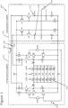
- FIG. 1 shows an example of a programmable gain amplifier (PGA) 100.
- the PGA 100 receives an input voltage signal (Vin) 103 and provides an output voltage signal (Vout) 104.
- the PGA 100 includes a transconductance amplifier 101 and a transimpedance amplifier 102.
- the transconductance amplifier 101 receives the input voltage signal (Vin) 103 and provides a transconductance amplifier current signal, in this example a differential transconductance amplifier current signal (I AB , -I AB ) 105, 106.
- the transfer function of the transconductance amplifier 101 is Gm.
- the transimpedance amplifier 102 provides the output voltage signal (Vout) 104 based on the differential transconductance amplifier current signal (I AB , - I AB ) 105, 106 received from the transconductance amplifier 101.
- the transfer function of the transimpedance amplifier 102 is Zm.
- the transconductance amplifier 101 includes a switchable resistance network 107, which comprises a plurality of gain-setting switches 108 that are configurable to set the gain of the PGA.
- the gain-setting switches 108 in the switchable resistance network 107 can be implemented as MOSFETs.
- the switchable resistance network 107 of Figure 1 has a plurality of branches in parallel with each other. Each branch is connected in series between the base of a first transistor (labelled as node A in Figure 1 ) and the base of a second transistor (labelled as node B in Figure 1 ). The first transistor and the second transistor are provided as part of a level shifter.
- Each branch of the switchable resistance network 107 includes a gain-setting switch 108 and a resistance 109a, 109b.
- the gain-setting switch 108 and the resistance 109a, 109b are in series with each other.
- the resistance in a branch is provided as a first resistor 109a and a second resistor 109b that have the same value.
- These resistors 109a, 109b are provided either side of the gain-setting switch 108 - an arrangement that serves to reduce the common mode voltage of the switch - such that a single branch includes the following components:
- the gain-setting switches 108 are openable and closable in accordance with a switch control signal to influence the gain of the programmable gain amplifier.
- the resistances in the branches do not have the same value such that a non-linear sequence of gain values is available.
- the resistance in each branch is expressed as a multiplier of a unit resistance (Ru).
- a first branch has a resistance value of Ru;
- a second branch has a resistance value of 2Ru;
- a third branch has a resistance value of 4Ru;
- a fourth branch has a resistance value of 8Ru;
- a fifth branch has a resistance value of 16Ru;
- a sixth branch has a resistance value of 32Ru;
- a seventh branch has a resistance value of 32Ru.
- the associated branch makes a contribution to the overall gain of the PGA 100.
- the size of the contribution of each branch depends on the value of the resistance in that branch.
- the operation of the transconductance amplifier 101 can be represented by the following equations (assuming that the gain-setting switches 108 are ideal; that is they do not have any leakage current and they do not have any resistance when the switch is on / closed (i.e. on-resistance, R ON )):
- V outp 48 R u ⁇ I outp
- V outm ⁇ 48 R u ⁇ I outm
- the switch control signals for the gain-setting switches 108 can take the following values in order to configure seven different gain values. Although it will be appreciated that different control signals (and indeed different resistance values in the branches of the switchable resistance network 107) can be used to provide different gain values.
- Examples of PGAs described herein can include a controller that provides the switch control signals for operating the switches such that the PGA 100 applies the required gain value to the input voltage signal (Vin) 103.
- One or more of the embodiments of the present disclosure that follow can reduce or eliminate the non-linearity such that a more accurate gain value can be applied by the PGA. As will be discussed below, this can be achieved by duplicating part of the transconductance amplifier 101, especially by providing switches that correspond to at least some of the gain-setting switches 108, but without the resistances in the switchable resistance network 107 (such that it does not significantly contribute to the gain of the PGA 100).
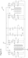
- FIG. 2 shows an example embodiment of a PGA 200 according to the present disclosure.
- Features of the PGA 200 of Figure 2 that are also shown in Figure 1 will be given corresponding reference numbers in the 200 series and will not necessarily be described again here.
- the PGA 200 of Figure 2 includes a switch leakage compensation circuit 210.
- the switch leakage compensation circuit 210 receives the input voltage signal 203 and outputs a compensation current signal, in this example a differential compensation current signal (I A'B' , -I A'B' ) 214, 215.
- the switch leakage compensation circuit 210 includes a compensation transconductance amplifier 218, and the compensation transconductance amplifier 218 comprises a switchable compensation resistance network 211.
- the majority of the compensation transconductance amplifier 218 is the same as the transconductance amplifier 201, with the exception of the switchable compensation resistance network 211.
- the compensation transconductance amplifier 218 provides bias conditions to the switchable compensation resistance network 211 that are the same as the bias conditions that are provided by the transconductance amplifier 201 to the switchable resistance network 207.
- the compensation transconductance amplifier 218 can have the same circuit layout and the same (or substantially similar) component values as the transconductance amplifier 201.
- the compensation transconductance amplifier 218 and the transconductance amplifier 201 can be implemented on the same integrated circuit (IC) such that any manufacturing tolerances that are present in the transconductance amplifier 201 are likely to be the same in the compensation transconductance amplifier 218.
- IC integrated circuit
- the switchable compensation resistance network 211 includes a plurality of branches in parallel with each other. Each branch is connected in series between the base of a third transistor (labelled as node A' in Figure 2 ) and the base of a fourth transistor (labelled as node B' in Figure 2 ).
- the third transistor 232 and the fourth transistor 233 are provided as part of a level shifter.
- the third transistor 232 of the switch leakage compensation circuit 210 can be considered as functionally equivalent to the first transistor 230 in the transconductance amplifier 201.
- the fourth transistor 233 of the switch leakage compensation circuit 210 can be considered as functionally equivalent to the second transistor 231 in the transconductance amplifier 201.
- Each branch of the switchable compensation resistance network 211 includes a gain-mimicking switch 212 in series with a leakage-current-conducting switch 213.
- Each gain-mimicking switch 212 has a corresponding gain-setting switch 208 in the switchable resistance network 207.
- Each gain-setting switch 208 in the switchable resistance network 207 does not necessarily have a corresponding gain-mimicking switch 212 in the switchable compensation resistance network 211.
- the switchable resistance network 207 has a seventh branch (with components labelled as 16Ru, sw6, 16RU in Figure 2 ) that does not have a corresponding branch in the switchable compensation resistance network 211.
- the gain-setting switch 208 in the seventh branch of the switchable resistance network 207 in this example is always closed during operation such that a minimum gain value (Av) of 3 is applied (as shown in the above table that illustrates one way in which the gain-setting switches 208 can be controlled to provide a plurality of different gain values). Therefore, there will not be any leakage current through the gain-setting switch 208 in the seventh branch of the switchable resistance network 207 when the PGA 200 is in use.
- the switchable resistance network 207 can thus have a branch that is always "on" to define a minimum gain value.
- Each gain-mimicking switch 212 is openable and closable in accordance with the same switch control signal that is used for the corresponding gain-setting switch 208. Furthermore, the characteristics of the gain-mimicking switches 212 are the same as the characteristics of the corresponding gain-setting switches 208. This can include the gain-mimicking switches 212 and the corresponding gain-setting switches 208 having the same size (especially when they are implemented on silicon). Therefore, the gain-mimicking switches 212 (labelled as swi' in Figure 2 ) have the same size and are operated according to the same control signals as the corresponding gain-setting switches 208 (labelled as swi in Figure 2 ).
- the leakage-current-conducting switches 213 are openable and closable in accordance with the inverse / complement of the switch control signal that is used to control the gain-mimicking switch 212 in the same branch. In this way, when the gain-mimicking switch 212 in the branch is open, the leakage-current-conducting switch 213 in the branch is closed, and vice versa. That is, when the gain-mimicking switch 212 in the branch is closed, the leakage-current-conducting switch 213 in the branch is open.
- the leakage-current-conducting switches 213 can be smaller than the gain-mimicking switches 212 (and therefore also smaller than the gain-setting switches 208) such that they contribute only a small amount of leakage current when they are open. In some applications, the leakage-current-conducting switches 213 can have the minimum size that is possible on an IC such that they contribute the minimum amount of leakage current when they are open.
- the branches of the switchable compensation resistance network 211 do not include any resistors (or at least no significant resistance beyond the inherent properties of the switches 212, 213) so that the differential compensation current signal (I A'B' , -I A'B' ) 214, 215 that is provided by the switch leakage compensation circuit 210 does not significantly affect the overall gain of the PGA 200.
- the same non-linear term that is highlighted in bold above for the transconductance amplifier 201 can be generated. As will be described below, this new term can be added with a negative sign to the differential transconductance amplifier current signals (I AB , 205, 206 from the (original) transconductance amplifier 201.
- the transimpedance amplifier 202 has a positive-input-terminal 223 and negative-input-terminal 224. As will be appreciated from the above description, the transimpedance amplifier 202 provides the output voltage signal (Vout) 204 based on differential input current signals I outp , I outm 216, 217 received at its positive-input-terminal 223 and negative-input-terminal 224. In this example, the transimpedance amplifier 202 receives the transconductance amplifier current signal (I AB and 205, 206 and the compensation current signal (I A'B' and -I A'B' ) 214, 215 such that they have opposite polarities to each other.
- the positive-input-terminal 223 of the transimpedance amplifier 202 is connected to a positive-output-terminal 220 of the transconductance amplifier 201, such that it receives a positive differential transconductance amplifier current signal I AB 205 from the transconductance amplifier 201.
- the negative-input-terminal 224 of the transimpedance amplifier 202 is connected to a negative-output-terminal 219 of the transconductance amplifier 201, such that it receives a negative differential transconductance amplifier current signal -I AB 206 from the transconductance amplifier 201.
- the switch leakage compensation circuit 210 also includes a positive-output-terminal 222 and a negative-output-terminal 221.
- the positive-output-terminal 222 provides a positive differential compensation current signal I A'B' 214.
- the negative-output-terminal 221 provides a negative differential compensation current signal -I A'B' 215.
- the positive-input-terminal 223 of the transimpedance amplifier 202 is connected to the negative-output-terminal 221 of the switch leakage compensation circuit 210, such that it receives the negative differential compensation current signal -I A'B' 215 from the switch leakage compensation circuit 210.
- the negative-input-terminal 224 of the transimpedance amplifier 202 is connected to the positive-output-terminal 222 of the switch leakage compensation circuit 210, such that it receives the positive differential compensation current signal I A'B' 214 from the switch leakage compensation circuit 210.
- the transimpedance amplifier 202 can provide the output voltage signal (Vout) 204 based on the difference between the transconductance amplifier current signal (I AB and 205, 206 from the transconductance amplifier 201 and the compensation current signal (I A'B' and -I A'B' ) 214, 215 from the switch leakage compensation circuit 210.
- the operation of the switch leakage compensation circuit 210 can be represented by the following equation (neglecting the leakage currents of the leakage-current-conducting switches 213, which is acceptable because they are much smaller than the gain-mimicking switches 212):
- I A ′ B ′ I sw 0 ′ ⁇ b 0 ⁇ + I sw 1 ′ ⁇ b 1 ⁇ + I sw 2 ′ ⁇ b 2 ⁇ + I sw 3 ′ ⁇ b 3 ⁇ + I sw 4 ′ ⁇ b 4 ⁇ + I sw 5 ′ ⁇ b 5 ⁇
- the transfer function (Gm) of a combination of the transconductance amplifier 201 and the switch leakage compensation circuit 210 can be represented as (with the newly added terms due to the switch leakage compensation circuit 210 shown in bold):
- V V out
- V in 96 ⁇ b 0 + 48 ⁇ b 1 + 24 ⁇ b 2 + 12 ⁇ b 3 + 6 ⁇ b 4 + 3 ⁇ b 5 + 3 ⁇ b 6 + 96 R u V in I sw 0 ⁇ I sw 0 ′ b 0 ⁇ + I sw 1 ⁇ I sw 1 ′ b 1 ⁇ + I sw 2 ⁇ I sw 2 b 2 ⁇ + I sw 3 ⁇ I sw 3 ′ b 3 ⁇ + I sw 4 ⁇ I sw 4 ′ b 4 ⁇ + I sw 5 ⁇ I sw 5 ′ b 5 ⁇
- V V out
- V in 96 ⁇ b 0 + 48 ⁇ b 1 + 24 ⁇ b 2 + 12 ⁇ b 3 + 6 ⁇ b 4 + 3 ⁇ b 5 + 3 ⁇ b 6
- the use of the switch leakage compensation circuit 210 removes the non-linearity in the transfer function that was identified above for the PGA of Figure 1 . This is because the transfer function no longer depends on Vin. Furthermore, the leakage currents through the open gain-setting switches 208 are cancelled out by corresponding leakage currents through the open gain-mimicking switches 212.
- the switch leakage compensation circuit 210 that has been added to the PGA architecture enables a gain value to be achieved that converges on the ideal gain Av that is identified earlier in this document. As a reminder, that ideal gain had been determined by considering ideal switches.
- This represents the minimum gain value that can be applied by the PGA 300. Applying such a minimum gain value can be considered as the worst-case scenario in terms of leakage current through the gain-setting switches. This is because only one gain-setting switch is closed and the rest are open. Correspondingly, all of the leakage-current-conducting switches 313 are closed.
- the linearity of the gain with respect to the input signal and temperature can be a very important specification.
- the linearity error is calculated with respect to an extrapolated gain obtained by two measures at temperature T0 and T1.
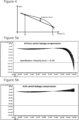
- Figure 4 illustrates the principle of this measure.
- the new PGA architecture (with the switch leakage compensation circuit of Figure 3 ) achieves an improvement in linearity by a factor of about 7 when the PGA 600 applies a gain value of 3.
- This represents the maximum gain value that can be applied by the PGA 600. Applying such a maximum gain value should not result in any leakage current through the gain-setting switches because they are all closed.
- all of the leakage-current-conducting switches 613 are open.
- the PGA 600 of Figure 6 is simulated to ensure that the inclusion of the switch leakage compensation circuit does not negatively affect the performance of the PGA 600 when it is not required.
- Embodiments of PGAs described herein can be beneficial when used as part of a High linearity Programmable Gain Amplifier or a High linearity Variable Gain Amplifier (VGA), for example.
- VGA High linearity Variable Gain Amplifier
- PGAs described herein can be used in any measurement chain for monitoring a voltage or a current.
- the PGA can be used to monitor current in a battery of an electrical vehicle.
- Such PGAs can also be associated with an analogue to digital converter (ADC) in a BMS (Battery Management System).
- ADC analogue to digital converter
- the set of instructions/method steps described above are implemented as functional and software instructions embodied as a set of executable instructions which are effected on a computer or machine which is programmed with and controlled by said executable instructions. Such instructions are loaded for execution on a processor (such as one or more CPUs).
- processor includes microprocessors, microcontrollers, processor modules or subsystems (including one or more microprocessors or microcontrollers), or other control or computing devices.
- a processor can refer to a single component or to plural components.
- the set of instructions/methods illustrated herein and data and instructions associated therewith are stored in respective storage devices, which are implemented as one or more non-transient machine or computer-readable or computer-usable storage media or mediums.
- Such computer-readable or computer usable storage medium or media is (are) considered to be part of an article (or article of manufacture).
- An article or article of manufacture can refer to any manufactured single component or multiple components.
- the non-transient machine or computer usable media or mediums as defined herein excludes signals, but such media or mediums may be capable of receiving and processing information from signals and/or other transient mediums.
- Example embodiments of the material discussed in this specification can be implemented in whole or in part through network, computer, or data based devices and/or services. These may include cloud, internet, intranet, mobile, desktop, processor, look-up table, microcontroller, consumer equipment, infrastructure, or other enabling devices and services. As may be used herein and in the claims, the following non-exclusive definitions are provided.
- one or more instructions or steps discussed herein are automated.
- the terms automated or automatically mean controlled operation of an apparatus, system, and/or process using computers and/or mechanical/electrical devices without the necessity of human intervention, observation, effort and/or decision.
- any components said to be coupled may be coupled or connected either directly or indirectly.
- additional components may be located between the two components that are said to be coupled.
Landscapes
- Engineering & Computer Science (AREA)
- Power Engineering (AREA)
- Physics & Mathematics (AREA)
- Nonlinear Science (AREA)
- Control Of Amplification And Gain Control (AREA)
Abstract
Description
- The present disclosure relates to a programmable gain amplifier (PGA).
- According to a first aspect of the present disclosure there is provided A programmable gain amplifier that is configured to receive an input voltage signal and provide an output voltage signal, wherein the programmable gain amplifier comprises:
- a transconductance amplifier, which is configured to receive the input voltage signal and provide a transconductance amplifier current signal, wherein the transconductance amplifier comprises a switchable resistance network that is configurable to set the gain of the programmable gain amplifier;
- a switch leakage compensation circuit, which is configured to receive the input voltage signal and output a compensation current signal, wherein the switch leakage compensation circuit comprises a compensation transconductance amplifier, and wherein the compensation transconductance amplifier comprises a switchable compensation resistance network;
- a transimpedance amplifier, which is configured to provide the output voltage signal based on the difference between the transconductance amplifier current signal from the transconductance amplifier and the compensation current signal from the switch leakage compensation circuit;
- the switchable resistance network comprises a plurality of branches in parallel with each other, wherein each branch includes:
- a gain-setting switch that is openable and closable in accordance with a switch control signal to influence the gain of the programmable gain amplifier; and
- a resistance in series with the gain-setting switch;
- the switchable compensation resistance network comprises a plurality of branches in parallel with each other, wherein each branch includes:
- a gain-mimicking switch that has a corresponding gain-setting switch in the switchable resistance network, wherein the gain-mimicking switch is openable and closable in accordance with the same switch control signal that is used for the corresponding gain-setting switch; and
- a leakage-current-conducting switch in series with the gain-mimicking switch, wherein the leakage-current-conducting switch is openable and closable in accordance with the complement of the switch control signal that is used to control the gain-mimicking switch in the same branch.
- In this way, when the gain-mimicking switch in the branch is open, the leakage-current-conducting switch in the branch is closed, and vice versa.
- Advantageously, use of the switch leakage compensation circuit can improve the linearity of the programmable gain amplifier.
- In one or more embodiments the gain-mimicking switches are configured to operate on the same bias conditions as their corresponding gain-setting switches.
- In one or more embodiments each gain-mimicking switch is the same size as its corresponding gain-setting switch.
- In one or more embodiments the transimpedance amplifier is configured to receive the transconductance amplifier current signal and the compensation current signal such that they have opposite polarities to each other.
- In one or more embodiments the transconductance amplifier current signal is a differential signal that comprises: a positive differential transconductance amplifier current signal; and a negative differential transconductance amplifier current signal. The compensation current signal may be a differential signal that comprises: a positive differential compensation current signal; and a negative differential compensation current signal. The transimpedance amplifier may comprise a positive-input-terminal and a negative-input-terminal. The transconductance amplifier may comprise: a positive-output-terminal, which is configured to provide the positive differential transconductance amplifier current signal; and a negative-output-terminal, which is configured to provide the negative differential transconductance amplifier current signal. The switch leakage compensation circuit may comprise: a positive-output-terminal, which is configured to provide the positive differential compensation current signal; and a negative-output-terminal, which is configured to provide the negative differential compensation current signal. The positive-input-terminal of the transimpedance amplifier may be connected to the positive-output-terminal of the transconductance amplifier. The positive-input-terminal of the transimpedance amplifier may be connected to the negative-output-terminal of the switch leakage compensation circuit. The negative-input-terminal of the transimpedance amplifier may be connected to the negative-output-terminal of the transconductance amplifier. The negative-input-terminal of the transimpedance amplifier may be connected to the positive-output-terminal of the switch leakage compensation circuit.
- In one or more embodiments the leakage-current-conducting-switches are smaller than the gain-mimicking switches.
- In one or more embodiments the branches of the switchable compensation resistance network do not include any resistors.
- In one or more embodiments a plurality of the branches in the switchable compensation resistance network comprise resistances with different resistance values.
- In one or more embodiments the compensation transconductance amplifier is the same as the transconductance amplifier, with the exception of the switchable resistance network and the switchable compensation resistance network.
- In one or more embodiments the circuit layout of the compensation transconductance amplifier is the same as the circuit layout of the transconductance amplifier.
- In one or more embodiments, with the exception of the switchable resistance network and the switchable compensation resistance network, the component values of components in the compensation transconductance amplifier are the same as component values of corresponding components in the transconductance amplifier.
- In one or more embodiments the switchable resistance network has a branch in which the gain-setting switch is always closed when the programmable gain array is in use in order to apply a minimum gain value.
- In one or more embodiments the switchable resistance network has a branch that does not have a corresponding branch in the switchable compensation resistance network.
- In one or more embodiments programmable gain amplifier further comprises a controller, where the controller is configured to provide switch control signals for operating the gain-setting switches, the gain-mimicking switches and the leakage-current-conducting switches such that the PGA applies a required gain value.
- There is also disclosed an integrated circuit comprising any programmable gain amplifier disclosed herein.
- While the disclosure is amenable to various modifications and alternative forms, specifics thereof have been shown by way of example in the drawings and will be described in detail. It should be understood, however, that other embodiments, beyond the particular embodiments described, are possible as well. All modifications, equivalents, and alternative embodiments falling within the spirit and scope of the appended claims are covered as well.
- The above discussion is not intended to represent every example embodiment or every implementation within the scope of the current or future Claim sets. The figures and Detailed Description that follow also exemplify various example embodiments. Various example embodiments may be more completely understood in consideration of the following Detailed Description in connection with the accompanying Drawings.
- One or more embodiments will now be described by way of example only with reference to the accompanying drawings in which:
-
Figure 1 shows an example of a programmable gain amplifier (PGA); -
Figure 2 shows an example embodiment of a PGA according to the present disclosure; -
Figure 3 illustrates the PGA ofFigure 2 configured to apply a gain value of 3; -
Figure 4 illustrates the principle of a measure of the linearity of the gain with respect to the input signal and temperature; -
Figure 5a shows a plot of gain error versus temperature for the PGA ofFigure 1 that is configured to apply a gain factor of 3; -
Figure 5b shows a plot of gain error versus temperature for the PGA ofFigure 3 that is configured to apply a gain factor of 3; -
Figure 6 illustrates the PGA ofFigure 2 configured to apply a gain value of 192; -
Figure 7a shows a plot of gain error versus temperature for the PGA ofFigure 1 that is configured to apply a gain factor of 192; and -
Figure 7b shows a plot of gain error versus temperature for the PGA ofFigure 6 that is configured to apply a gain factor of 192. - A programmable gain amplifier (PGA) can apply a gain value (also known as a gain factor) to an input voltage signal to provide an output voltage signal. The gain value that is applied by the PGA can be selected from a plurality (N) of gain values by controlling the states of a plurality of switches. To realize the functionality of the switches, MOSFETs (metal oxide semiconductor field effect transistors) can be used, which can have one of two states / positions: "open" and "closed". The PGA has N gain possibilities and can be implemented with N-1 switches that can be "opened" or "closed" depending on the required gain. However, when a MOSFET is used as a switch, it is not ideal. When the MOSFET is "open" there is a current leakage. This current leakage depends on the size of the MOSFET and can increase with temperature. This temperature dependence can be problematic in providing an accurate gain value.
-
Figure 1 shows an example of a programmable gain amplifier (PGA) 100. ThePGA 100 receives an input voltage signal (Vin) 103 and provides an output voltage signal (Vout) 104. - The
PGA 100 includes atransconductance amplifier 101 and atransimpedance amplifier 102. Thetransconductance amplifier 101 receives the input voltage signal (Vin) 103 and provides a transconductance amplifier current signal, in this example a differential transconductance amplifier current signal (IAB, -IAB) 105, 106. The transfer function of thetransconductance amplifier 101 is Gm. Thetransimpedance amplifier 102 provides the output voltage signal (Vout) 104 based on the differential transconductance amplifier current signal (IAB, - IAB) 105, 106 received from thetransconductance amplifier 101. The transfer function of thetransimpedance amplifier 102 is Zm. By combining the transfer functions of thetransconductance amplifier 101 and the transimpedance amplifier 102 (Gm and Zm) we obtain the transfer function of the PGA:
- The
transconductance amplifier 101 includes aswitchable resistance network 107, which comprises a plurality of gain-settingswitches 108 that are configurable to set the gain of the PGA. As indicated above, the gain-settingswitches 108 in theswitchable resistance network 107 can be implemented as MOSFETs. - The
switchable resistance network 107 ofFigure 1 has a plurality of branches in parallel with each other. Each branch is connected in series between the base of a first transistor (labelled as node A inFigure 1 ) and the base of a second transistor (labelled as node B inFigure 1 ). The first transistor and the second transistor are provided as part of a level shifter. Each branch of theswitchable resistance network 107 includes a gain-settingswitch 108 and aresistance switch 108 and theresistance first resistor 109a and asecond resistor 109b that have the same value. Theseresistors - a
first resistor 109a having a first terminal and a second terminal, wherein the first terminal of thefirst resistor 109a is connected to the base of the first transistor (node A); - a
second resistor 109b having a first terminal and a second terminal wherein the first terminal of thesecond resistor 109b is connected to the base of the second transistor (node B); and - a gain-setting
switch 108 that is connected between the second terminal of thefirst resistor 109a and the second terminal of thesecond resistor 109b. - The gain-setting
switches 108 are openable and closable in accordance with a switch control signal to influence the gain of the programmable gain amplifier. In this example, the resistances in the branches do not have the same value such that a non-linear sequence of gain values is available. The resistance in each branch is expressed as a multiplier of a unit resistance (Ru). In this example: a first branch has a resistance value of Ru; a second branch has a resistance value of 2Ru; a third branch has a resistance value of 4Ru; a fourth branch has a resistance value of 8Ru; a fifth branch has a resistance value of 16Ru; a sixth branch has a resistance value of 32Ru; a seventh branch has a resistance value of 32Ru. - As will be discussed in detail below, when a gain-setting
switch 108 is closed, the associated branch makes a contribution to the overall gain of thePGA 100. The size of the contribution of each branch depends on the value of the resistance in that branch. - The operation of the
transconductance amplifier 101 can be represented by the following equations (assuming that the gain-settingswitches 108 are ideal; that is they do not have any leakage current and they do not have any resistance when the switch is on / closed (i.e. on-resistance, RON)):

- Where:
- Ioutp 116 and Ioutm 117 are the differential input current signals for the
transimpedance amplifier 102; - IAB 105 and -
I AB 106 are the differential transconductance amplifier current signals that are provided as the output signals of thetransconductance amplifier 101; -
V in 103 is the input voltage; - bi is the switch control signal for setting the state of the ith gain-setting switch swi (bi = 0 → swi open; and bi = 1 → swi closed); and
- Ru is the unit resistance.
- The overall transconductance amplifier current signal (Iout) provided by the
transconductance amplifier 101, which is a differential current signal in this example, can be written as:
- The transfer function (Gm) of the
transconductance amplifier 101 is:
- The operation of the
transimpedance amplifier 102 can be represented by the following equations:


- Where:
- Voutp is the voltage that is provided at a first voltage output terminal, based on a positive one of the differential input current signals (IOUTP) 116 for the
transimpedance amplifier 101; - Voutm is the voltage that is provided at a second voltage output terminal, based on a negative one of the differential input current signals (IOUTM) 117 for the
transimpedance amplifier 101; and - Vout is the
output voltage 104. - The transfer function (Zm) of the
transimpedance amplifier 102 is:
- The overall transfer function (Av) of the PGA is:

- In this example, the switch control signals for the gain-setting
switches 108 can take the following values in order to configure seven different gain values. Although it will be appreciated that different control signals (and indeed different resistance values in the branches of the switchable resistance network 107) can be used to provide different gain values.b0b1b2b3b4b5b6 sw0 sw1 sw2 sw3 sw4 sw5 sw6 AV 0000001 opened opened opened opened opened opened closed 3 0000011 opened opened opened opened opened closed closed 6 0000111 opened opened opened opened closed closed closed 12 0001111 opened opened opened closed closed closed closed 24 0011111 opened opened closed closed closed closed closed 48 0111111 opened closed closed closed closed closed closed 96 1111111 closed closed closed closed closed closed closed 192 - Examples of PGAs described herein can include a controller that provides the switch control signals for operating the switches such that the
PGA 100 applies the required gain value to the input voltage signal (Vin) 103. - We will now rewrite some of the same previous equations, but include the leakage current of the gain-setting switches 108. This more accurately reflects the real-world operation of the gain-setting switches 108. The on-resistance, RON, will still be ignored, however, because it is so much smaller than the
resistances PGA 100. - The operation of the transconductance amplifier 101 can now be represented by the following equations (with the newly added terms in bold):


- Where:
- Iswi is the leakage current through the ith gain-setting
switch 108; and - b̅l is the inverse of the switch control signal for setting the state of the ith gain-setting
switch 108. - The overall transfer function (Av) of the PGA can then be represented as (again, with the newly added terms in bold):

- This equation for the overall transfer function (Av) of the PGA shows a non-linearity term in bold; this is because the expression depends on Vin. This non-linearity term is problematic in that it can negatively affect the accuracy with which a desired gain value can be applied.
- One or more of the embodiments of the present disclosure that follow can reduce or eliminate the non-linearity such that a more accurate gain value can be applied by the PGA. As will be discussed below, this can be achieved by duplicating part of the
transconductance amplifier 101, especially by providing switches that correspond to at least some of the gain-settingswitches 108, but without the resistances in the switchable resistance network 107 (such that it does not significantly contribute to the gain of the PGA 100). -
Figure 2 shows an example embodiment of aPGA 200 according to the present disclosure. Features of thePGA 200 ofFigure 2 that are also shown inFigure 1 will be given corresponding reference numbers in the 200 series and will not necessarily be described again here. - In addition to the components of
Figure 1 , thePGA 200 ofFigure 2 includes a switchleakage compensation circuit 210. The switchleakage compensation circuit 210 receives theinput voltage signal 203 and outputs a compensation current signal, in this example a differential compensation current signal (IA'B', -IA'B') 214, 215. - The switch
leakage compensation circuit 210 includes acompensation transconductance amplifier 218, and thecompensation transconductance amplifier 218 comprises a switchablecompensation resistance network 211. The majority of thecompensation transconductance amplifier 218 is the same as thetransconductance amplifier 201, with the exception of the switchablecompensation resistance network 211. In this way, thecompensation transconductance amplifier 218 provides bias conditions to the switchablecompensation resistance network 211 that are the same as the bias conditions that are provided by thetransconductance amplifier 201 to theswitchable resistance network 207. With the exception of the switchablecompensation resistance network 211, thecompensation transconductance amplifier 218 can have the same circuit layout and the same (or substantially similar) component values as thetransconductance amplifier 201. Advantageously, thecompensation transconductance amplifier 218 and thetransconductance amplifier 201 can be implemented on the same integrated circuit (IC) such that any manufacturing tolerances that are present in thetransconductance amplifier 201 are likely to be the same in thecompensation transconductance amplifier 218. - The switchable
compensation resistance network 211 includes a plurality of branches in parallel with each other. Each branch is connected in series between the base of a third transistor (labelled as node A' inFigure 2 ) and the base of a fourth transistor (labelled as node B' inFigure 2 ). Thethird transistor 232 and the fourth transistor 233 are provided as part of a level shifter. Thethird transistor 232 of the switchleakage compensation circuit 210 can be considered as functionally equivalent to thefirst transistor 230 in thetransconductance amplifier 201. The fourth transistor 233 of the switchleakage compensation circuit 210 can be considered as functionally equivalent to thesecond transistor 231 in thetransconductance amplifier 201. - Each branch of the switchable
compensation resistance network 211 includes a gain-mimickingswitch 212 in series with a leakage-current-conductingswitch 213. Each gain-mimickingswitch 212 has a corresponding gain-settingswitch 208 in theswitchable resistance network 207. Each gain-settingswitch 208 in theswitchable resistance network 207 does not necessarily have a corresponding gain-mimickingswitch 212 in the switchablecompensation resistance network 211. For instance, in the example ofFigure 2 , theswitchable resistance network 207 has a seventh branch (with components labelled as 16Ru, sw6, 16RU inFigure 2 ) that does not have a corresponding branch in the switchablecompensation resistance network 211. This is because the gain-settingswitch 208 in the seventh branch of theswitchable resistance network 207 in this example is always closed during operation such that a minimum gain value (Av) of 3 is applied (as shown in the above table that illustrates one way in which the gain-settingswitches 208 can be controlled to provide a plurality of different gain values). Therefore, there will not be any leakage current through the gain-settingswitch 208 in the seventh branch of theswitchable resistance network 207 when thePGA 200 is in use. Theswitchable resistance network 207 can thus have a branch that is always "on" to define a minimum gain value. - Each gain-mimicking
switch 212 is openable and closable in accordance with the same switch control signal that is used for the corresponding gain-settingswitch 208. Furthermore, the characteristics of the gain-mimickingswitches 212 are the same as the characteristics of the corresponding gain-setting switches 208. This can include the gain-mimickingswitches 212 and the corresponding gain-settingswitches 208 having the same size (especially when they are implemented on silicon). Therefore, the gain-mimicking switches 212 (labelled as swi' inFigure 2 ) have the same size and are operated according to the same control signals as the corresponding gain-setting switches 208 (labelled as swi inFigure 2 ). - The leakage-current-conducting
switches 213 are openable and closable in accordance with the inverse / complement of the switch control signal that is used to control the gain-mimickingswitch 212 in the same branch. In this way, when the gain-mimickingswitch 212 in the branch is open, the leakage-current-conductingswitch 213 in the branch is closed, and vice versa. That is, when the gain-mimickingswitch 212 in the branch is closed, the leakage-current-conductingswitch 213 in the branch is open. - The leakage-current-conducting
switches 213 can be smaller than the gain-mimicking switches 212 (and therefore also smaller than the gain-setting switches 208) such that they contribute only a small amount of leakage current when they are open. In some applications, the leakage-current-conductingswitches 213 can have the minimum size that is possible on an IC such that they contribute the minimum amount of leakage current when they are open. - The branches of the switchable
compensation resistance network 211 do not include any resistors (or at least no significant resistance beyond the inherent properties of theswitches 212, 213) so that the differential compensation current signal (IA'B', -IA'B') 214, 215 that is provided by the switchleakage compensation circuit 210 does not significantly affect the overall gain of thePGA 200. - By including a leakage-current-conducting
switch 213 in cascade with each gain-mimickingswitch 212, and by operating the leakage-current-conductingswitches 213 with complementary commands to those for the associated gain-mimickingswitches 212, the same non-linear term that is highlighted in bold above for thetransconductance amplifier 201 can be generated. As will be described below, this new term can be added with a negative sign to the differential transconductance amplifier current signals (IAB, 205, 206 from the (original)transconductance amplifier 201. - The
transimpedance amplifier 202 has a positive-input-terminal 223 and negative-input-terminal 224. As will be appreciated from the above description, thetransimpedance amplifier 202 provides the output voltage signal (Vout) 204 based on differential input current signals Ioutp, Ioutm 216, 217 received at its positive-input-terminal 223 and negative-input-terminal 224. In this example, thetransimpedance amplifier 202 receives the transconductance amplifier current signal (IAB and 205, 206 and the compensation current signal (IA'B' and -IA'B') 214, 215 such that they have opposite polarities to each other. - The positive-input-
terminal 223 of thetransimpedance amplifier 202 is connected to a positive-output-terminal 220 of thetransconductance amplifier 201, such that it receives a positive differential transconductance amplifier current signal IAB 205 from thetransconductance amplifier 201. The negative-input-terminal 224 of thetransimpedance amplifier 202 is connected to a negative-output-terminal 219 of thetransconductance amplifier 201, such that it receives a negative differential transconductance amplifier current signal -IAB 206 from thetransconductance amplifier 201. - The switch
leakage compensation circuit 210 also includes a positive-output-terminal 222 and a negative-output-terminal 221. The positive-output-terminal 222 provides a positive differential compensationcurrent signal I A'B' 214. The negative-output-terminal 221 provides a negative differential compensation current signal -I A'B' 215. The positive-input-terminal 223 of thetransimpedance amplifier 202 is connected to the negative-output-terminal 221 of the switchleakage compensation circuit 210, such that it receives the negative differential compensation current signal -IA'B' 215 from the switchleakage compensation circuit 210. The negative-input-terminal 224 of thetransimpedance amplifier 202 is connected to the positive-output-terminal 222 of the switchleakage compensation circuit 210, such that it receives the positive differential compensation current signal IA'B' 214 from the switchleakage compensation circuit 210. In this way, thetransimpedance amplifier 202 can provide the output voltage signal (Vout) 204 based on the difference between the transconductance amplifier current signal (IAB and 205, 206 from thetransconductance amplifier 201 and the compensation current signal (IA'B' and -IA'B') 214, 215 from the switchleakage compensation circuit 210. - The operation of the switch
leakage compensation circuit 210 can be represented by the following equation (neglecting the leakage currents of the leakage-current-conductingswitches 213, which is acceptable because they are much smaller than the gain-mimicking switches 212):
- Where:
- IA'B' is the positive differential compensation
current signal 214 that is provided as an output of the switchleakage compensation circuit 210; - Iswi' is the leakage current through the
i th 212 gain-mimickingswitch 212; and - b̅l is the inverse of the switch control signal for setting the state of the corresponding ith gain-setting
switch 208. - The positive differential input current signal (Ioutp) 216 for the
transimpedance amplifier 202 ofFigure 2 is (with the newly added terms due to the switchleakage compensation circuit 210 shown in bold):
- It will be appreciated that similar equations can be written for the negative differential input current signal (Ioutm) 217.
- The transfer function (Gm) of a combination of the
transconductance amplifier 201 and the switchleakage compensation circuit 210 can be represented as (with the newly added terms due to the switchleakage compensation circuit 210 shown in bold):
- This equation can be rewritten to highlight an important part of the expression:

- In this equation, we can remove the term in the box if Iswi = Iswi'. This is because the term in the box will equal zero. This condition is true at the first order (neglecting any mismatch between the switches, which is assumed to be negligible) because the gain-setting switches 208 (swi) and the gain-mimicking switches 212 (swi') are identical (in terms of type of component and size) and they are biased in the same way.
- Even if mismatch between the switches is not neglected, the term of the expression that is shown in the box will be greatly reduced such that it is not problematic for the performance of the
PGA 200. - The transfer function of the PGA can be written as:
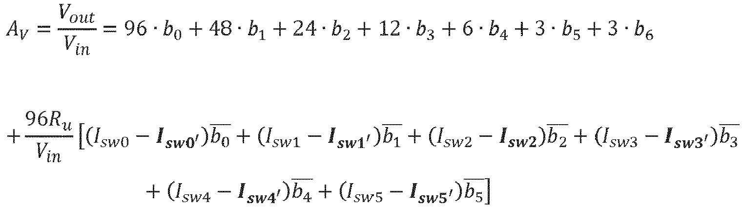
- Assuming that there is no mismatch, this previous expression can be simplified to:

- Therefore, it can be seen that the use of the switch
leakage compensation circuit 210 removes the non-linearity in the transfer function that was identified above for the PGA ofFigure 1 . This is because the transfer function no longer depends on Vin. Furthermore, the leakage currents through the open gain-settingswitches 208 are cancelled out by corresponding leakage currents through the open gain-mimickingswitches 212. The switchleakage compensation circuit 210 that has been added to the PGA architecture enables a gain value to be achieved that converges on the ideal gain Av that is identified earlier in this document. As a reminder, that ideal gain had been determined by considering ideal switches. - We will now describe some simulation results for the PGA of
Figure 2 , implemented on silicon. -
Figure 3 illustrates the PGA ofFigure 2 configured to apply a gain value of 3 (Av = 3) by closing only the gain-setting switch in the seventh branch of theswitchable resistance network 307 in thetransconductance amplifier 301. This represents the minimum gain value that can be applied by thePGA 300. Applying such a minimum gain value can be considered as the worst-case scenario in terms of leakage current through the gain-setting switches. This is because only one gain-setting switch is closed and the rest are open. Correspondingly, all of the leakage-current-conductingswitches 313 are closed. - For this kind of block, the linearity of the gain with respect to the input signal and temperature can be a very important specification. In the following simulations, we focus on the gain linearity with respect to the temperature. The linearity error is calculated with respect to an extrapolated gain obtained by two measures at temperature T0 and T1.
Figure 4 illustrates the principle of this measure. -
Figure 5a shows a plot of gain error (in milli-percent) on the horizontal axis versus temperature on the vertical axis, for several process cases, for the PGA ofFigure 1 (i.e. one without switch leakage compensation) that is configured to apply a gain factor of 3 (Av = 3).Figure 5b shows a plot of gain error (in milli-percent) on the horizontal axis versus temperature on the vertical axis, for several process cases, for the PGA ofFigure 3 (i.e. one with switch leakage compensation) that is configured to apply a gain factor of 3 (Av = 3). - The table below compares results of both of the PGA architectures that are illustrated in
Figures 5a and 5b .Linearity error (%) Without leakage compensation With leakage compensation min -154m -7.2m max 3.2m 21m - It can be seen that the new PGA architecture (with the switch leakage compensation circuit of
Figure 3 ) achieves an improvement in linearity by a factor of about 7 when thePGA 600 applies a gain value of 3. -
Figure 6 illustrates the PGA ofFigure 2 configured to apply a gain value of 192 (Av = 192) by closing all of the gain-setting switches in theswitchable resistance network 607 in thetransconductance amplifier 601. This represents the maximum gain value that can be applied by thePGA 600. Applying such a maximum gain value should not result in any leakage current through the gain-setting switches because they are all closed. Correspondingly, all of the leakage-current-conductingswitches 613 are open. ThePGA 600 ofFigure 6 is simulated to ensure that the inclusion of the switch leakage compensation circuit does not negatively affect the performance of thePGA 600 when it is not required. -
Figure 7a shows a plot of gain error (in milli-percent) on the horizontal axis versus temperature on the vertical axis, for several process cases, for the PGA ofFigure 1 (i.e. one without switch leakage compensation) that is configured to apply a gain factor of 192 (Av = 192).Figure 7b shows a plot of gain error (in milli-percent) on the horizontal axis versus temperature on the vertical axis, for several process cases, for the PGA ofFigure 6 (i.e. one with switch leakage compensation) that is configured to apply a gain factor of 192 (Av = 192). - The table below compares results of both of the PGA architectures that are illustrated in
Figures 7a and 7b .Linearity error (%) Without leakage compensation With leakage compensation min -7.86m -7.86m max 35.98m 36m - It can be seen that the linearity error is the same when applying a gain value of 192, both with and without the switch leakage compensation circuit. Therefore, even when the switch leakage compensation circuit is not required, it does not perturb the performance of the original architecture.
- Embodiments of PGAs described herein can be beneficial when used as part of a High linearity Programmable Gain Amplifier or a High linearity Variable Gain Amplifier (VGA), for example.
- Furthermore, embodiments of PGAs described herein can be used in any measurement chain for monitoring a voltage or a current. In one application, the PGA can be used to monitor current in a battery of an electrical vehicle. Such PGAs can also be associated with an analogue to digital converter (ADC) in a BMS (Battery Management System).
- The instructions and/or flowchart steps in the above figures can be executed in any order, unless a specific order is explicitly stated. Also, those skilled in the art will recognize that while one example set of instructions/method has been discussed, the material in this specification can be combined in a variety of ways to yield other examples as well, and are to be understood within a context provided by this detailed description.
- In some example embodiments the set of instructions/method steps described above are implemented as functional and software instructions embodied as a set of executable instructions which are effected on a computer or machine which is programmed with and controlled by said executable instructions. Such instructions are loaded for execution on a processor (such as one or more CPUs). The term processor includes microprocessors, microcontrollers, processor modules or subsystems (including one or more microprocessors or microcontrollers), or other control or computing devices. A processor can refer to a single component or to plural components.
- In other examples, the set of instructions/methods illustrated herein and data and instructions associated therewith are stored in respective storage devices, which are implemented as one or more non-transient machine or computer-readable or computer-usable storage media or mediums. Such computer-readable or computer usable storage medium or media is (are) considered to be part of an article (or article of manufacture). An article or article of manufacture can refer to any manufactured single component or multiple components. The non-transient machine or computer usable media or mediums as defined herein excludes signals, but such media or mediums may be capable of receiving and processing information from signals and/or other transient mediums.
- Example embodiments of the material discussed in this specification can be implemented in whole or in part through network, computer, or data based devices and/or services. These may include cloud, internet, intranet, mobile, desktop, processor, look-up table, microcontroller, consumer equipment, infrastructure, or other enabling devices and services. As may be used herein and in the claims, the following non-exclusive definitions are provided.
- In one example, one or more instructions or steps discussed herein are automated. The terms automated or automatically (and like variations thereof) mean controlled operation of an apparatus, system, and/or process using computers and/or mechanical/electrical devices without the necessity of human intervention, observation, effort and/or decision.
- It will be appreciated that any components said to be coupled may be coupled or connected either directly or indirectly. In the case of indirect coupling, additional components may be located between the two components that are said to be coupled.
- In this specification, example embodiments have been presented in terms of a selected set of details. However, a person of ordinary skill in the art would understand that many other example embodiments may be practiced which include a different selected set of these details. It is intended that the following claims cover all possible example embodiments.
Claims (15)
- A programmable gain amplifier that is configured to receive an input voltage signal and provide an output voltage signal, wherein the programmable gain amplifier comprises:a transconductance amplifier, which is configured to receive the input voltage signal and provide a transconductance amplifier current signal, wherein the transconductance amplifier comprises a switchable resistance network that is configurable to set the gain of the programmable gain amplifier;a switch leakage compensation circuit, which is configured to receive the input voltage signal and output a compensation current signal, wherein the switch leakage compensation circuit comprises a compensation transconductance amplifier, and wherein the compensation transconductance amplifier comprises a switchable compensation resistance network;a transimpedance amplifier, which is configured to provide the output voltage signal based on the difference between the transconductance amplifier current signal from the transconductance amplifier and the compensation current signal from the switch leakage compensation circuit;wherein:the switchable resistance network comprises a plurality of branches in parallel with each other, wherein each branch includes:a gain-setting switch that is openable and closable in accordance with a switch control signal to influence the gain of the programmable gain amplifier; anda resistance in series with the gain-setting switch;the switchable compensation resistance network comprises a plurality of branches in parallel with each other, wherein each branch includes:a gain-mimicking switch that has a corresponding gain-setting switch in the switchable resistance network, wherein the gain-mimicking switch is openable and closable in accordance with the same switch control signal that is used for the corresponding gain-setting switch; anda leakage-current-conducting switch in series with the gain-mimicking switch, wherein the leakage-current-conducting switch is openable and closable in accordance with the complement of the switch control signal that is used to control the gain-mimicking switch in the same branch such that when the gain-mimicking switch in the branch is open, the leakage-current-conducting switch in the branch is closed, and vice versa.
- The programmable gain amplifier of claim 1, wherein the gain-mimicking switches are configured to operate on the same bias conditions as their corresponding gain-setting switches.
- The programmable gain amplifier of claim 1 or claim 2, wherein each gain-mimicking switch is the same size as its corresponding gain-setting switch.
- The programmable gain amplifier of any preceding claim, wherein the transimpedance amplifier is configured to receive the transconductance amplifier current signal and the compensation current signal such that they have opposite polarities to each other.
- The programmable gain amplifier of any preceding claim, wherein:the transconductance amplifier current signal is a differential signal that comprises: a positive differential transconductance amplifier current signal; and a negative differential transconductance amplifier current signal;the compensation current signal is a differential signal that comprises: a positive differential compensation current signal; and a negative differential compensation current signal;the transimpedance amplifier comprises a positive-input-terminal and a negative-input-terminal;the transconductance amplifier comprises:a positive-output-terminal, which is configured to provide the positive differential transconductance amplifier current signal; anda negative-output-terminal, which is configured to provide the negative differential transconductance amplifier current signal;the switch leakage compensation circuit comprises:a positive-output-terminal, which is configured to provide the positive differential compensation current signal; anda negative-output-terminal, which is configured to provide the negative differential compensation current signal;the positive-input-terminal of the transimpedance amplifier is connected to the positive-output-terminal of the transconductance amplifier;the positive-input-terminal of the transimpedance amplifier is connected to the negative-output-terminal of the switch leakage compensation circuit;the negative-input-terminal of the transimpedance amplifier is connected to the negative-output-terminal of the transconductance amplifier; andthe negative-input-terminal of the transimpedance amplifier is connected to the positive-output-terminal of the switch leakage compensation circuit.
- The programmable gain amplifier of any preceding claim, wherein the leakage-current-conducting-switches are smaller than the gain-mimicking switches.
- The programmable gain amplifier of any preceding claim, wherein the branches of the switchable compensation resistance network do not include any resistors.
- The programmable gain amplifier of any preceding claim, wherein a plurality of the branches in the switchable compensation resistance network comprise resistances with different resistance values.
- The programmable gain amplifier of any preceding claim, wherein the compensation transconductance amplifier is the same as the transconductance amplifier, with the exception of the switchable resistance network and the switchable compensation resistance network.
- The programmable gain amplifier of any preceding claim, wherein the circuit layout of the compensation transconductance amplifier is the same as the circuit layout of the transconductance amplifier.
- The programmable gain amplifier of any preceding claim, wherein, with the exception of the switchable resistance network and the switchable compensation resistance network, the component values of components in the compensation transconductance amplifier are the same as component values of corresponding components in the transconductance amplifier.
- The programmable gain amplifier of any preceding claim, wherein the switchable resistance network has a branch in which the gain-setting switch is always closed when the programmable gain array is in use in order to apply a minimum gain value.
- The programmable gain amplifier of any preceding claim, wherein the switchable resistance network has a branch that does not have a corresponding branch in the switchable compensation resistance network.
- The programmable gain amplifier of any preceding claim, further comprising a controller, wherein the controller is configured to provide switch control signals for operating the gain-setting switches, the gain-mimicking switches and the leakage-current-conducting switches such that the PGA applies a required gain value.
- An integrated circuit comprising the programmable gain amplifier of any preceding claim.
Priority Applications (3)
| Application Number | Priority Date | Filing Date | Title |
|---|---|---|---|
| EP22306353.8A EP4340220A1 (en) | 2022-09-15 | 2022-09-15 | A programmable gain amplifier |
| CN202311018472.5A CN117713707A (en) | 2022-09-15 | 2023-08-14 | Programmable gain amplifier |
| US18/464,551 US20240106403A1 (en) | 2022-09-15 | 2023-09-11 | Programmable gain amplifier |
Applications Claiming Priority (1)
| Application Number | Priority Date | Filing Date | Title |
|---|---|---|---|
| EP22306353.8A EP4340220A1 (en) | 2022-09-15 | 2022-09-15 | A programmable gain amplifier |
Publications (1)
| Publication Number | Publication Date |
|---|---|
| EP4340220A1 true EP4340220A1 (en) | 2024-03-20 |
Family
ID=83594068
Family Applications (1)
| Application Number | Title | Priority Date | Filing Date |
|---|---|---|---|
| EP22306353.8A Pending EP4340220A1 (en) | 2022-09-15 | 2022-09-15 | A programmable gain amplifier |
Country Status (3)
| Country | Link |
|---|---|
| US (1) | US20240106403A1 (en) |
| EP (1) | EP4340220A1 (en) |
| CN (1) | CN117713707A (en) |
Citations (3)
| Publication number | Priority date | Publication date | Assignee | Title |
|---|---|---|---|---|
| WO2002097979A2 (en) * | 2001-05-25 | 2002-12-05 | Infineon Technologies Ag | Programmable logarithmic gain adjustment for open-loop amplifiers |
| US20060001491A1 (en) * | 2004-06-30 | 2006-01-05 | Stmicroelectronics, S.A. | Fast transconductance amplifier |
| US20130314158A1 (en) * | 2012-05-24 | 2013-11-28 | Hitachi, Ltd. | Semiconductor device and communication device |
-
2022
- 2022-09-15 EP EP22306353.8A patent/EP4340220A1/en active Pending
-
2023
- 2023-08-14 CN CN202311018472.5A patent/CN117713707A/en active Pending
- 2023-09-11 US US18/464,551 patent/US20240106403A1/en active Pending
Patent Citations (3)
| Publication number | Priority date | Publication date | Assignee | Title |
|---|---|---|---|---|
| WO2002097979A2 (en) * | 2001-05-25 | 2002-12-05 | Infineon Technologies Ag | Programmable logarithmic gain adjustment for open-loop amplifiers |
| US20060001491A1 (en) * | 2004-06-30 | 2006-01-05 | Stmicroelectronics, S.A. | Fast transconductance amplifier |
| US20130314158A1 (en) * | 2012-05-24 | 2013-11-28 | Hitachi, Ltd. | Semiconductor device and communication device |
Non-Patent Citations (1)
| Title |
|---|
| SAVOJ JAFAR ET AL: "A Low-Power 0.5-6.6 Gb/s Wireline Transceiver Embedded in Low-Cost 28 nm F", IEEE JOURNAL OF SOLID-STATE CIRCUITS, IEEE, USA, vol. 48, no. 11, 19 October 2013 (2013-10-19), pages 2582 - 2594, XP011531074, ISSN: 0018-9200, [retrieved on 20131021], DOI: 10.1109/JSSC.2013.2274824 * |
Also Published As
| Publication number | Publication date |
|---|---|
| CN117713707A (en) | 2024-03-15 |
| US20240106403A1 (en) | 2024-03-28 |
Similar Documents
| Publication | Publication Date | Title |
|---|---|---|
| US10579086B2 (en) | Current source calibration tracking temperature and bias current | |
| EP2779462B1 (en) | Clock signal error correction in a digital-to-analog converter | |
| US20200026993A1 (en) | Neural network circuit | |
| US20140085117A1 (en) | Sampling circuit, a method of reducing distortion in a sampling circuit, and an analog to digital converter including such a sampling circuit | |
| US20130154740A1 (en) | Techniques for pga linearity | |
| CN107145182A (en) | Input voltage pattern intends resistor and resistance control method | |
| CN101663812A (en) | Method and apparatus for linearizing a transconductor by distortion | |
| KR20230086734A (en) | Impedance calibration circuit and method | |
| EP3250933B1 (en) | Correction circuits for successive-approximation-register analog-to-digital converters | |
| US7777655B2 (en) | Wideband switched current source | |
| US20190165800A1 (en) | Multiplying DAC of pipelined ADC | |
| US20240106403A1 (en) | Programmable gain amplifier | |
| US6621439B1 (en) | Method for implementing a segmented current-mode digital/analog converter with matched segment time constants | |
| CN107037760A (en) | A kind of input current type artifical resistance device and resistance control method | |
| US10742175B2 (en) | Amplifier circuit, reception circuit, and semiconductor integrated circuit | |
| US7295068B2 (en) | Increasing the linearity of a transconductance cell | |
| CN119030638B (en) | Calibration system and calibration method for receiver signal link | |
| US11509326B2 (en) | Sigma-delta analogue to digital converter | |
| CN114696823A (en) | Compensation circuit, method and device for audio DAC and storage medium | |
| US12418302B2 (en) | Sigma-delta analogue to digital converter | |
| CN113839674A (en) | Analog-digital conversion circuit | |
| CN110022110B (en) | Voice coil motor damping control circuit | |
| JP2023554501A (en) | Highly linear multiplier | |
| JP2022525384A (en) | Electronically controlled resistor | |
| US20150137855A1 (en) | Current To Voltage Converter |
Legal Events
| Date | Code | Title | Description |
|---|---|---|---|
| PUAI | Public reference made under article 153(3) epc to a published international application that has entered the european phase |
Free format text: ORIGINAL CODE: 0009012 |
|
| STAA | Information on the status of an ep patent application or granted ep patent |
Free format text: STATUS: THE APPLICATION HAS BEEN PUBLISHED |
|
| AK | Designated contracting states |
Kind code of ref document: A1 Designated state(s): AL AT BE BG CH CY CZ DE DK EE ES FI FR GB GR HR HU IE IS IT LI LT LU LV MC MK MT NL NO PL PT RO RS SE SI SK SM TR |
|
| STAA | Information on the status of an ep patent application or granted ep patent |
Free format text: STATUS: REQUEST FOR EXAMINATION WAS MADE |
|
| 17P | Request for examination filed |
Effective date: 20240920 |
|
| RBV | Designated contracting states (corrected) |
Designated state(s): AL AT BE BG CH CY CZ DE DK EE ES FI FR GB GR HR HU IE IS IT LI LT LU LV MC MK MT NL NO PL PT RO RS SE SI SK SM TR |