EP4339628A1 - Measurement system, related integrated circuit and method - Google Patents
Measurement system, related integrated circuit and method Download PDFInfo
- Publication number
- EP4339628A1 EP4339628A1 EP23194464.6A EP23194464A EP4339628A1 EP 4339628 A1 EP4339628 A1 EP 4339628A1 EP 23194464 A EP23194464 A EP 23194464A EP 4339628 A1 EP4339628 A1 EP 4339628A1
- Authority
- EP
- European Patent Office
- Prior art keywords
- capacitance
- electronic switch
- terminal
- measurement system
- voltage
- Prior art date
- Legal status (The legal status is an assumption and is not a legal conclusion. Google has not performed a legal analysis and makes no representation as to the accuracy of the status listed.)
- Granted
Links
Images






Classifications
-
- H—ELECTRICITY
- H03—ELECTRONIC CIRCUITRY
- H03F—AMPLIFIERS
- H03F3/00—Amplifiers with only discharge tubes or only semiconductor devices as amplifying elements
- H03F3/45—Differential amplifiers
- H03F3/45071—Differential amplifiers with semiconductor devices only
- H03F3/45076—Differential amplifiers with semiconductor devices only characterised by the way of implementation of the active amplifying circuit in the differential amplifier
- H03F3/45475—Differential amplifiers with semiconductor devices only characterised by the way of implementation of the active amplifying circuit in the differential amplifier using IC blocks as the active amplifying circuit
-
- G—PHYSICS
- G01—MEASURING; TESTING
- G01R—MEASURING ELECTRIC VARIABLES; MEASURING MAGNETIC VARIABLES
- G01R27/00—Arrangements for measuring resistance, reactance, impedance, or electric characteristics derived therefrom
- G01R27/02—Measuring real or complex resistance, reactance, impedance, or other two-pole characteristics derived therefrom, e.g. time constant
- G01R27/26—Measuring inductance or capacitance; Measuring quality factor, e.g. by using the resonance method; Measuring loss factor; Measuring dielectric constants ; Measuring impedance or related variables
- G01R27/2605—Measuring capacitance
-
- H—ELECTRICITY
- H03—ELECTRONIC CIRCUITRY
- H03F—AMPLIFIERS
- H03F1/00—Details of amplifiers with only discharge tubes, only semiconductor devices or only unspecified devices as amplifying elements
- H03F1/26—Modifications of amplifiers to reduce influence of noise generated by amplifying elements
-
- H—ELECTRICITY
- H03—ELECTRONIC CIRCUITRY
- H03F—AMPLIFIERS
- H03F3/00—Amplifiers with only discharge tubes or only semiconductor devices as amplifying elements
- H03F3/45—Differential amplifiers
- H03F3/45071—Differential amplifiers with semiconductor devices only
- H03F3/45076—Differential amplifiers with semiconductor devices only characterised by the way of implementation of the active amplifying circuit in the differential amplifier
- H03F3/45179—Differential amplifiers with semiconductor devices only characterised by the way of implementation of the active amplifying circuit in the differential amplifier using MOSFET transistors as the active amplifying circuit
- H03F3/45273—Mirror types
-
- H—ELECTRICITY
- H03—ELECTRONIC CIRCUITRY
- H03F—AMPLIFIERS
- H03F2200/00—Indexing scheme relating to amplifiers
- H03F2200/261—Amplifier which being suitable for instrumentation applications
Definitions
- the embodiments of the present description refer measurement systems, such as capacitive sensors.
- Capacitive sensors are commonly used.
- such capacitive sensor may have a high resolution, low complexity and low temperature-dependency.
- such capacitive sensors may be used in microelectromechanical systems (MEMS) based sensors, such as accelerometers, position sensors, pressure sensors, and moisture sensors.
- MEMS microelectromechanical systems
- Recently, such capacitive sensors have also been used for Laboratory on a Chip (LoC) applications, e.g ., for DNA protein interaction quantification, cellular monitoring, bio-particle detection, organic solvent monitoring, sensing of droplet parameters, bacteria detection, etc.
- LoC Laboratory on a Chip
- a capacitive sensor comprises at least one couple of sensing electrodes that are connected to an interface readout circuit.
- Figure 1 shows a typical LoC application, wherein two electrodes 100 and 102 implemented with a conductive material, are arranged on an integrated circuit 20.
- the electrodes 100 and 102 are connected to an interface circuit, e.g ., implemented within the integrated circuit 20, which is configured to generate an analog or digital signal by measuring a value being indicative of the capacitance value between the electrodes 100 and 102.
- a processing circuit e.g ., implemented within the integrated circuit 20, may be configured to provide an estimate of the physical, biological and/or chemical properties of the sample 104 as a function of the measured capacitance value.
- CMOS Complementary Metal-Oxide-Semiconductor
- CMOS capacitive sensing techniques have been proposed in literature for different LoC applications.
- One of the most commonly used technique is the charge-based capacitance measurement (CBCM).
- CBCM charge-based capacitance measurement
- Figure 2 shows an example of an interface circuit 30 according to the CBCM technique.
- the electrodes 100 and 102 form a sense capacitance/capacitor Cs, wherein the capacitance value of the sense capacitance Cs is usually indicative of the physical, biological and/or chemical properties of a sample 104 in the vicinity of the electrodes 100 and 102.
- a first electronic switch M 4 such as a transistor, such as an n-channel Field-effect transistor (FET), such as an n-channel Metal-Oxide-Semiconductor (MOS) FET, is connected ( e.g ., directly) in parallel with the sense capacitance Cs, i.e ., the electronic switch M 4 is connected between the electrodes 100 and 102, and is thus configured to selectively short-circuit the sense capacitance Cs as a function of a control signal ⁇ 2 received at a control terminal of the electronic switch M 4 , e.g ., the gate terminal of a corresponding FET.
- FET Field-effect transistor
- MOS Metal-Oxide-Semiconductor
- the interface circuit comprises a second electronic switch M 2 , such as a transistor, such as an p-channel Field-effect transistor (FET), such as an p-channel MOSFET, configured to selectively connect the sense capacitance Cs to a supply voltage VDD as a function of a control signal ⁇ 1 received at a control terminal of the electronic switch M 2 , e.g ., the gate terminal of a corresponding FET.
- a control signal ⁇ 1 received at a control terminal of the electronic switch M 2 , e.g ., the gate terminal of a corresponding FET.
- the electrode 102 of the capacitance Cs is connected to a first reference voltage, e.g ., ground GND, and the electrode 100 is connected via the electronic switch M 2 to a second reference voltage, e.g ., a supply voltage VDD of the integrated circuit 20.
- a control circuit 36 may be configured to generate the control signals ⁇ 1 and ⁇ 2 in order to selectively charge and discharge the sense capacitance Cs.
- control circuit 36 is configured to generate the control signals ⁇ 1 and ⁇ 2 according to switching cycles having a duration/period T S .
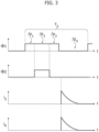
- each switching cycle T S comprises a sequence of the following four phases:
- phase ⁇ t 2 is used to reset the charge of the capacitance Cs and the phase ⁇ t 4 is used to charge the capacitance Cs.
- the phases ⁇ t 1 and ⁇ t 3 are purely optional and are used to avoid that the electronic switches M 2 and M 4 generate a short-circuit by connecting the supply voltage VDD to ground.
- the interface circuit 30 may comprise a measurement circuit 34 configured to measure the charge or discharge current is flowing through the capacitance Cs.
- the measurement circuit 34 comprises a current sensor 340 connected between the electronic switch M 2 and the supply voltage VDD, thereby monitoring the charge current.
- the CBCM technique uses also a second branch, which comprises a reference capacitance C R .
- the reference capacitance C R has the same physical structure as the sense capacitance C S , but is not exposed to the sample 104.
- the capacitance value of the sense capacitance Cs varies and usually increases, i.e ., Cs > C R .
- the second branch comprises:
- the electronic switch M 3 is driven via the control signal ⁇ 2 and the electronic switch M 1 is driven via the control signal ⁇ 1 .
- the reference capacitance C R is reset during the phase ⁇ t 2 and is charged during the phase ⁇ t 4 , thereby generating a current flow i R .
- the interface circuit 30 may comprise a current sensor 342 configured to measure the charge or discharge current i R flowing through the capacitance C R .
- the current sensor 342 is connected between the electronic switch M 1 and the supply voltage VDD, thereby monitoring the charge current.
- the interface circuit 30 comprises a first half-bridge implemented with the electronic switches M 2 and M 4 , wherein the first half-bridge is configured to selectively apply a first reference voltage (usually the supply voltage VDD) or a second reference voltage (usually ground GND) to a first terminal/electrode 100 of the sense capacitance Cs, wherein the second terminal/electrode 102 of the sense capacitance Cs is connected to the second reference voltage (usually ground GND).
- a first reference voltage usually the supply voltage VDD
- a second reference voltage usually ground GND
- the interface circuit 30 comprises a second half-bridge implemented with the electronic switches M 1 and M 3 , wherein the second half-bridge is configured to selectively apply the first reference voltage (usually the supply voltage VDD) or the second reference voltage (usually ground GND) to a first terminal/electrode of the reference capacitance C R wherein the second terminal/electrode of the reference capacitance C R is connected to the second reference voltage (usually ground GND).
- the two half-bridges are identified as CBCM cell 32.
- the electronic switches M 3 and M 4 are usually implemented with n-channel MOSFETs and the electronic switches M 1 and M 2 are usually implemented with p-channel MOSFETs.
- the source terminals of the n-channel FETs M 3 and M 4 are connected to the second reference voltage (e.g ., ground GND)
- the source terminals of the p-channel FETs M 1 and M 2 are connected to the first reference voltage (e.g ., VDD)
- the drain terminals of the n-channel FET M 4 and the p-channel FET M 2 are connected to the first terminal/electrode of the sense capacitance Cs
- the drain terminals of the n-channel FET M 3 and the p-channel FET M 1 are connected to the first terminal/electrode of the reference capacitance C R .
- Figure 4 shows a first example of a measurement circuit of the CBCM cell 32 configured to generate a signal indicative of the difference ⁇ i between the currents is and i R .
- a solution is disclosed in Saghi Forouhi, Rasoul Dehghani, and Ebrahim Ghafar-Zadeh, "Toward High Throughput Core-CBCM CMOS Capacitive Sensors for Life Science Applications: A Novel Current Mode for High Dynamic Range Circuitry", Sensors 2018 .
- the measurement circuit of the CBCM cell 32 comprises a first current mirror 3400, e.g ., implemented with two p-channel FETs, configured to generate a current is' by mirroring the (charge) current is provided to the CBCM cell 32.
- This mirrored current is' is used to charge a first capacitance C int+ , which essentially operates as an integrator configured to convert the current is'(t) into a voltage.
- the measurement circuit of the CBCM cell 32 comprises a second current mirror 3410, e.g ., implemented with two p-channel FETs, configured to generate a current i R ' by mirroring the (charge) current i R provided to the CBCM cell 32.
- This mirrored current i R ' is used to charge a second capacitance C int- , which essentially operates as an integrator configured to convert the current i R '(t) into a voltage.
- a differential amplifier 3420 may be used to generate a signal, e.g ., a voltage V out , by amplifying the difference between the voltage at the capacitance C int+ and the voltage at the capacitance C int- .
- a signal e.g ., a voltage V out
- the voltage at the capacitance C int+ is connected to the positive input terminal of the differential amplifier 3420 and the voltage at the capacitance C int- is connected to the negative input terminal of the differential amplifier 3420.
- the capacitances C int+ and C int- have the same capacitance value.
- the measurement circuit 34 also comprises electronic switches 3402 and 3412 in order to selectively discharge the capacitances C int+ and C int- , e.g ., as a function of a reset signal RST.
- the circuit of Figure 4 permits to execute a plurality of the switching cycles T S shown in Figure 3 , whereby each time the current pulse in the currents is and i R are transferred to the capacitances C int+ and C int- , respectively.
- a first drawback relates to the fact the output V out is also a function of the threshold V thp , which depends on temperature and process spread variations. Moreover, in this approach, to achieve a higher sensitivity, high voltages across the integrating capacitors C int+ and C int- are required. However, this situation may push the differential amplifier 3420 to a nonlinear region, and thus limits the resolution of the sensor circuit. To mitigate this second problem, the previously cited article by Saghi Forouhi also discloses an alternative approach, which is shown in Figure 5 .
- the current mirrors 3400 and 3410 are again configured to generate mirrored currents is' and i R ', respectively.
- a further current mirror 3430 e.g ., implemented with n-channel FETs, is used to generate a further mirrored current i R " by mirroring the current iR'.
- the output of the current mirror 3400 is connected in series with a capacitance C int .
- the output of the current mirror 3430 is connected in parallel with the capacitance C int .
- the circuit of Figure 5 permits to execute a plurality of the switching cycles shown in Figure 3 , whereby each time the current pulse in the current ix is transferred to the capacitances C int .
- the above object is achieved by a measurement system having the distinctive elements set forth specifically in the ensuing claims.
- Embodiments moreover concern a related integrated circuit and method.
- the measurement system comprises a first capacitance and a second capacitance.
- the measurement system comprises moreover a switching circuit configured to receive a first and a second control signal.
- the switching circuit In response to determining that the first control signal is asserted, the switching circuit connects a first terminal of the first capacitance to a first voltage and a first terminal of the second capacitance to a second voltage.
- the switching circuit in response to determining that the second control signal is asserted, connects the first terminal of the first capacitance and the first terminal of the second capacitance to a reference voltage, e.g ., ground.
- a control circuit is configured to generate the first and the second control signal according to switching cycles comprising four intervals. Specifically, for a first interval, the control circuit de-asserts the first and the second control signal. For a following second interval, the control circuit de-asserts the first control signal and asserts the second control signal, thereby connecting the first capacitance to the first voltage and the second capacitance to the second voltage. For a following third interval, the control circuit de-asserts the first and the second control signal. Finally, for a following fourth interval, the control circuit asserts the first control signal and de-asserts the second control signal, thereby connecting the first capacitance and the second capacitance to the reference voltage.
- the measurement system comprises further a measurement circuit, which in turn comprises a differential integrator and a comparator with hysteresis.
- the differential integrator comprises a differential operational amplifier, a first integration capacitance and a second integration capacitance.
- an inverting input of the differential operational amplifier is connected to a second terminal of the first capacitance and a non-inverting input of the differential operational amplifier is connected to a second terminal of the second capacitance.
- a first terminal of the first integration capacitance is connected to the inverting input of the differential operational amplifier and a second terminal of the first integration capacitance is connected via a first electronic switch to a positive output terminal of the differential operational amplifier, wherein the second terminal of the first integration capacitance represents a first output node of the differential integrator.
- the differential integrator comprises moreover a third electronic switch connected between the inverting input of the differential operational amplifier and the positive output terminal of the operational amplifier, and a fourth electronic switch connected between the non-inverting input of the differential operational amplifier and the negative output terminal of the operational amplifier.
- the comparator with hysteresis is configured to, in response to determining that a voltage applied to a negative input terminal of the comparator with hysteresis exceeds a voltage applied to a positive input terminal of the comparator with hysteresis plus a hysteresis threshold, set a first output terminal of the comparator with hysteresis to high and a second output terminal of the comparator with hysteresis to low.
- the comparator with hysteresis comprises a fifth electronic switch connected between the negative input of the comparator with hysteresis and the second output terminal of the comparator with hysteresis, and a sixth electronic switch connected between the positive input of the comparator with hysteresis and the first output terminal of the comparator with hysteresis.
- a first decoupling capacitance is connected between the negative input of the comparator with hysteresis and the first output node of the differential integrator, and a second decoupling capacitance connected between the positive input of the comparator with hysteresis and the second output node of the differential integrator.
- the measurement system is configured to manage a normal operation phase and a reset phase.
- the measurement system is configured to close the first electronic switch and the second electronic switch, in response to determining that the second control signal is asserted. Conversely, the measurement system is configured to open the first electronic switch and the second electronic switch in response to determining that the second control signal is de-asserted. Moreover, the measurement system is configured to close the third electronic switch and the fourth electronic switch in response to determining that the first control signal is asserted, and open the third electronic switch and the fourth electronic switch in response to determining that the first control signal is de-asserted.
- the first integration capacitance and the second integration capacitance are connected into the feedback paths of the differential operational amplifier, thereby permitting a charge transfer from the first and second capacitances to the first and second integration capacitances.
- the first and the second capacitances have a different charge when the first voltage and the second voltage correspond to a common voltage, but the first capacitance corresponds to a sense capacitance and the second capacitance corresponds to a reference capacitance.
- the voltage between the first and second output nodes of the differential integrator is indicative of the difference between the capacitances of the sense capacitance and the reference capacitance.
- the voltage between the first and second output nodes of the differential integrator is indicative of the difference between the first voltage and the second voltage.
- the comparator with hysteresis is thus operative, i.e ., the fifth electronic switch and the sixth electronic switch are opened.
- the measurement system monitors also a reset request signal during the normal operation phase and, in response to determining that the reset request signal indicates a reset request, the measurement system starts the reset phase.
- the measurement system is configured to assert the reset request signal after a given maximum number of the switching cycles, and/or in response to determining that the first output terminal of the comparator with hysteresis is set to high and/or the second output terminal of the comparator with hysteresis is set to low.
- the measurement system executes one or more sub-phases. Specifically, for a first reset interval, the measurement system closes the first, second, third, fourth, fifth and sixth electronic switches. Conversely, for a following second reset interval, the measurement system may open the third and fourth electronic switches and keeps closed the first, second, fifth and sixth electronic switches. Finally, at the end of the reset phase, e.g., at the end of second phase, the measurement system starts again the normal operation phase.
- the offsets and most of the flicker noise of the differential operational amplifier and the comparator with hysteresis may be stored to the decoupling capacitance during the first reset interval.
- the charge-injection and clock-feedthrough of the third and fourth electronic switches may be stored to the decoupling capacitance.
- the differential integrator may receive a first reset signal, and the third electronic switch and the fourth electronic switch may be configured to be closed in response to determining that the first control signal is asserted or the first reset signal is asserted.
- the comparator with hysteresis may be configured to receive a second reset signal, wherein the fifth electronic switch and the sixth electronic switch are configured to be closed in response to determining that the second reset signal is asserted.
- the measurement system may be configured to, while the control circuit asserts the second control signal, assert the first reset signal and the second reset signal for the first reset interval, and de-assert the first reset signal and assert the second reset signal for the second reset interval.
- the measurement system may comprise a delay circuit configured to generate the second reset signal by delaying the first reset signal.
- various embodiments relate to a corresponding method of operating such a measurement system. Specifically, during a normal operation phase, the method closes the first electronic switch and the second electronic switch in response to determining that the second control signal is asserted, and opens the first electronic switch and the second electronic switch in response to determining that the second control signal is de-asserted. Moreover, the method closes the third electronic switch and the fourth electronic switch in response to determining that the first control signal is asserted, and opens the third electronic switch and the fourth electronic switch in response to determining that the first control signal is de-asserted. In various embodiments, when using the fifth electronic switch and the sixth electronic switch, the method may also open the fifth electronic switch and the sixth electronic switch during a normal operation phase.
- the method may monitor a reset request signal indicating a reset request and start a reset phase in response to determining that the reset request signal indicates a reset request. Specifically, during the reset phase, the method closes the first, second, third, fourth electronic switches for a first reset interval. Moreover, when using the fifth and sixth electronic switches, the method may close the fifth and sixth electronic switches.
- the measurement system comprises the decoupling capacitances. Next, the method starts again the normal operation phase.
- the method may also open the third and fourth electronic switches and keep closed the first, second, fifth and sixth electronic switches for a following second reset interval following the first reset interval (and before the normal operation mode is started again).
- various embodiments of the present disclosure relate to a measurement system.
- Figure 6 shows an embodiment of a measurement system according to the present disclosure.
- a measurement system may be integrated in an integrated circuit 40.
- the measurement system comprises a switching circuit 32a comprising three terminals:
- the voltages V 1 and V 2 may also correspond to the same voltage, indicated in the following as voltage V A .
- the measurement system may comprise a voltage generator 42 configured to receive a supply voltage VDD, e.g ., via a pad/pin of the integrated circuit 40, and generate the voltage V A based on this supply voltage VDD.
- the measurement system has associated two capacitances C 1 and C 2 . These capacitances are preferably integrated in the measurement system for best matching. In general, the capacitance has two terminals T 1 and T 2 , and the capacitance has two terminals T 3 and T 4 .
- the switching circuit 32a receives a first control signal ⁇ 1 and a secondo control signal ⁇ 2 .
- the control signal ⁇ 1 and ⁇ 2 may be generated by a control circuit 36a of the measurement system.
- the control circuit 36a may be configured to generate the control signals ⁇ 1 and ⁇ 2 according to switching cycles having a duration/period Ts, wherein each switching cycle T S comprises a sequence of the following four phases:
- the switching circuit 32a is configured to:
- the switching circuit 32a is configured to apply the reference voltage V ref , or the voltages V 1 and V 2 , to the terminals T 1 and T 3 of the capacitances C 1 and C 2 , respectively.
- a measurement circuit 34a is configured to monitor a current i 1 flowing through the capacitance C 1 and a current i 2 flowing through the capacitance C 2 .
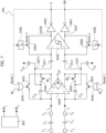
- Figure 7 shows an embodiment of a measurement circuit 34a according to the present disclosure.
- the measurement circuit 34a is implemented with a switched capacitor (SC) differential integrator.
- the differential integrator comprises a differential operational amplifier 3440, wherein the inverting/negative input terminal of the operational amplifier 3440 is connected ( e.g ., directly) to the terminal T 2 of the capacitance C 1 , and the non-inverting/positive input terminal of the operational amplifier 3440 is connected ( e.g ., directly) to the terminal T 4 of the capacitance C 2 .
- the differential integrator comprises:
- the electronic switches 3448 and 3450 are driven by the signal ⁇ 2 , and are closed when the signal ⁇ 2 is asserted. Accordingly, in the embodiment considered, the electronic switches 3448 and 3450 are closed when the signal ⁇ 2 is asserted, i.e ., during the discharge phase, thereby connecting the integration capacitances C I1 and C I2 into the feedback paths of the operation amplifier 3440.
- the first and second integration capacitance C I1 and C I2 have the same capacitance C I .
- the capacitances C I1 and C I2 may be implemented with internal capacitors for best matching with the capacitances C 1 and C 2 .
- the current path of an electronic switch 3452 is connected ( e.g ., directly) between the inverting/negative input terminal of the operational amplifier 3440 and the positive output terminal of the operational amplifier 3440
- the current path of an electronic switch 3454 is connected ( e.g ., directly) between the non-inverting/positive input terminal of the operational amplifier 3440 and the negative output terminal of the operational amplifier 3440.
- the electronic switches 3452 and 3454 are driven by the signal ⁇ 1 , and are closed when the signal ⁇ 1 is asserted. Accordingly, the electronic switches 3452 and 3454 are closed when the signal ⁇ 1 is asserted, i.e ., during the charge phase, thereby short-circuiting the feedback paths of the operation amplifier 3440.
- the differential operational amplifier 3440 has also associated a respective common mode voltage V CM , which may be fixed or settable.
- the input terminals of the operational amplifier 3440 are set to the common mode voltage V CM , which permits to charge the capacitances C 1 and C 2 via the voltages V 1 and Vz.
- the integration capacitances C I1 and C I2 are connected to the operational amplifier 3440 and the previously charged capacitances C 1 and C 2 discharge to the reference voltage V ref /ground GND.
- the charge applied to the capacitances C 1 and C 2 is different, e.g ., when:
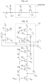
- Figures 8A, 8B and 8C show possible embodiments of the switching circuit 32a and the capacitances C 1 and Cz.
- the capacitance C 1 corresponds to a sense capacitance Cs and the capacitance C 2 corresponds to a reference capacitance C R , i.e ., the capacitance Cs has a variable capacitance value.
- the voltages V 1 and V 2 are connected to a common voltage V A , which may be provided via a terminal/pad/pin of the measurement system or via the voltage generator 42.
- the switching circuit 32a of Figure 8A essentially corresponds to the switching circuit 32 shown in Figure 2 .
- a first electronic switch M 4 such as a transistor, such as an n-channel FET, such as an n-channel MOSFET
- the current path of a second electronic switch M 2 such as a transistor, such as an p-channel Field-effect transistor (FET), such as an p-channel MOSFET, is connected ( e.g ., directly) between the terminal T 1 and the voltage V A .
- FET p-channel Field-effect transistor
- a third electronic switch M 3 such as a transistor, such as an n-channel FET, such as an n-channel MOSFET, is connected ( e.g ., directly) between the terminal T 3 and the reference voltage V ref /ground GND.
- a fourth electronic switch M 1 such as a transistor, such as an p-channel Field-effect transistor (FET), such as an p-channel MOSFET, is connected ( e.g ., directly) between the terminal T 3 and the voltage V A .
- FET p-channel Field-effect transistor
- the switches M 1 and M 2 are indeed closed when the signal ⁇ 1 is set to low.
- the control circuit 36a is configured to assert the signal ⁇ 1 by setting signal ⁇ 1 to high, indeed the inverted signal ⁇ 1 may be used to drive the gate terminal of the p-channel FETs M 1 and M 2 (see also Figure 8A ).
- the two half-bridges formed by the switches M 1 /M 3 and M 2 /M 4 indeed operate in parallel based on the same control signals.
- the electronic switches M 1 and M 3 may be omitted, and the terminal T 3 of the reference capacitance C R may be connected ( e.g ., directly) to the terminal T 1 of the sense capacitance Cs.
- the capacitances C 1 and C 2 have the same value Cs. Moreover, the voltages V 1 is connected to a voltage V in+ and the voltages V 2 is connected to a voltage V in- .
- a first electronic switch M 4 such as a transistor, such as an n-channel FET, such as an n-channel MOSFET
- a second electronic switch M 2 such as a transistor, such as an p-channel Field-effect transistor (FET), such as an p-channel MOSFET
- FET field-effect transistor
- a third electronic switch M 3 such as a transistor, such as an n-channel FET, such as an n-channel MOSFET, is connected ( e.g ., directly) between the terminal T 3 and the reference voltage V ref /ground GND.
- a fourth electronic switch M 1 such as a transistor, such as an p-channel Field-effect transistor (FET), such as an p-channel MOSFET, is connected ( e.g ., directly) between the terminal T 3 and the voltage V in- .
- FET p-channel Field-effect transistor
- the embodiments shown in Figures 8A and 8B may be used to monitor the difference ⁇ C between the capacitances Cs and C R
- the embodiment shown in Figure 8C may be used to monitor the amplitude of a differential voltage ⁇ V in corresponding to the difference between the voltages V in+ and V in- .
- the differential voltage V O,AMP is maintained stored at the intermediate nodes between the integration capacitances (C I1 or C I2 ) and the electronic switch (3448 or 3450).
- the second terminal of the integration capacitance Cn i.e ., the intermediate node between the capacitance Cn and the electronic switch 3448
- the second terminal of the integration capacitance C I2 i.e ., the intermediate node between the capacitance C I2 and the electronic switch 3450
- the output terminals OUT+ and OUT- provide a differential voltage V O , e.g ., corresponding to the previously indicated voltages V O,AMP .
- the signal S may be provided to a terminal/pad/pin of the measurement system or, as shown in Figure 6 , to a digital and/or analog processing circuit 44 of the measurement system.
- the processing circuit 44 may be a microprocessor programmed via software instructions.
- the signal S is generated via a differential comparator with hysteresis 3446 configured to assert the signal S when the voltage V O exceeds the hysteresis threshold of the comparator 3446.
- such a comparator with hysteresis 3446 comprises two input terminals for receiving a differential voltage ⁇ V CMP and two output terminals form providing signals OUT and OUTN, wherein the comparator 3446 is configured to set the signal OUT to high and the signal OUTN to low in response to determining that the voltage at the negative input terminal exceeds the voltage at the positive input terminal plus a first hysteresis voltage V H1 of the comparator. Similarly, the comparator 3446 is configured to set the signal OUT to low and the signal OUTN to high in response to determining that the voltage at the negative input terminal falls below the voltage at the positive input terminal minus a second hysteresis voltage V H2 .
- the first hysteresis voltage V H1 and the second hysteresis voltage V H2 have the same absolute value V H .
- the signal S may correspond, e.g ., to the signal OUT.
- the measurement circuit 34a comprises a first inverter 3460 configured to generate the signal S by inverting the signal OUTN.
- the measurement circuit 34a comprises preferably also a second inverter 3462 configured to generate a signal SN by inverting the signal OUT.
- these inverters 3460 and 3462 are useful in case the signals S and/or SN are used to drive other circuits, and may also be useful in order to balance the output terminals of the comparator with hysteresis 3446.
- the inverters 3460 and 3462 may also be replaced with a more complex driver stage, e.g ., comprising a cascade of inverters and/or other logic gates.
- the input terminals of the comparator 3446 are not connected directly to the nodes OUT+ and OUT-, but one of the input terminals of the comparator 3446, e.g ., the negative input terminal, is connected ( e.g ., directly) via a first capacitance/capacitor C DEC1 to the node OUT+ and the other input terminal of the comparator 3446, e.g ., the positive input terminal, is connected ( e.g ., directly) via a second capacitance/capacitor C DEC2 to the node OUT-.
- These capacitances C DEC1 and C DEC2 have the same capacitance value C DEC .
- these capacitances C DEC1 and C DEC2 represent decoupling capacitances between the integrator and the comparator, which thus only transfer the variations of the voltages at the nodes OUT+ and OUT- to the input terminals of the comparator.
- the offsets and most of the flicker noise of the operational amplifier 3440 and the comparator with hysteresis 3446 may be stored to the capacitances C DEC1 and C DEC2 during a reset phase whereby these voltages are then cancelled during the subsequent sensing operation.
- an asynchronous reset is performed once the signal S is asserted, i.e ., the signal S corresponds to a reset signal Reset1.
- the integrator 3440 may be reset by short-circuiting the integration capacitances C I1 and C I2 .
- the integration capacitances C I1 and C I2 are reset, when the electronic switches 3448, 3450, 3452 and 3454 are closed contemporaneously.
- the electronic switches 3452 and 3454 are closed when the signal ⁇ 1 is asserted or the reset signal Reset1/S is asserted.
- the electronic switches 3452 and 3454 are driven via logic OR gates 3442 and 3444 configured to combine the signals ⁇ 1 and Reset1.
- the comparator with hysteresis 3446 is reset during the reset phase.
- the comparator 3446 is reset by closing an electronic switch 3464 configured to short-circuit the output terminal OUTN and the negative input terminal of the comparator 3446 and an electronic switch 3466 configured to short-circuit the output terminal OUT and the positive input terminal of the comparator 3446.
- the electronic switches 3464 and 3466 are closed when the signal Reset1 is asserted. Conversely, in the embodiment shown in Figure 7 , the electronic switches 3464 and 3466 are closed when a reset signal Reset2 is asserted, wherein the reset signal Reset2 corresponds to the reset signal Reset1 with a given delay t D .
- the reset signal Reset2 may be generated via a delay circuit 3456, such as a delay line, receiving the reset signal Reset1 as input.
- Figure 7 shows a first delay circuit 3456 configured to generate the drive signal of the electronic switch 3464 by delaying the signal Reset1, and a second delay circuit 3458 configured to generate the drive signal of the electronic switch 3466 by delaying the signal Reset1.
- the offsets and most of the flicker noise of the operational amplifier 3440 and the comparator with hysteresis 3446 are stored to the capacitances C DEC1 and C DEC2 during the interval between the instants t 1 and t 2 .
- the charge-injection and clock-feedthrough of the switches 3452 and 3454 may be stored to the capacitances C DEC1 and C DEC2 .
- V error ⁇ Q SW /C DEC , wherein the voltage V error is usually in the micro-Volt range, and usually can be neglected or anyway absorbed by the comparator hysteresis.
- a smaller threshold voltage V H1 permits a faster detection, e.g ., of the sample passing over the electrodes 100 and 102 forming the capacitance Cs.
- a smaller threshold voltage V H1 may imply thermal noise and the charge injection/clock feedthrough mismatch of the switches 3464 and 3466 driven by the signal Reset2 on the measurement.
- the reset of the measurement circuit 34a may also be managed based on a timeout, which is used to trigger similar reset phases of the integrator and the comparator.
- the measurement system comprises a reset circuit configured to execute, in response to a reset request signal indicating a reset request, such as a rising edge of the signal S, a signal indicating that a given maximum number N of switching cycles have been executed, etc., the following phases in sequence:
- these switches may be equipped with dummy switches and/or capacitor Cx is added.
- a first capacitor C X1 is connected ( e.g ., directly) between the terminal OUT+ and a reference voltage, such as ground GND
- a second capacitor C X2 is connected ( e.g ., directly) between the terminal OUT- and the reference voltage, such as ground GND.
- the capacitors C X1 and C X2 have the same capacitance value.
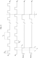
- Figure 10 shows a possible implementation of each of the switches 3448 and 3450.
- a first terminal of a respective integration capacitance C I1 or C I2 is connected to a respective input terminal of the operational amplifier 3440 and the electronic switch 3448/3450 is connected between the second terminal of the respective integration capacitance C I and a respective output node of the operational amplifier 3440, wherein the intermediate node between the integration capacitance C I and the electronic switch 3448/3450 corresponds to an output node OUT+ or OUT- of the integrator, generically indicated as node OUT.
- a capacitor C X1 or C X2 may be connected between the output node OUT and a reference voltage, e.g ., ground GND.
- each electronic switch 3448/3450 is implemented with a series connection of two FETs Q1 and Q2, such as n-channel FETs.
- the first FET Q1 is driven via the signal ⁇ 2 .
- the second FET Q2 is a dummy switch, wherein the source and drain terminals of the FET Q2 are short-circuited.
- the gate terminal of the FET Q2 is driven via a signal being asserted when the signal ⁇ 2 is de-asserted, such as the inverted version of the signal ⁇ 2 or preferably the signal ⁇ 1 .
- the FET Q1 has a given size ratio W 1 /L 1 (channel width/length), and the FET has a ratio W 2 /L 2 corresponding to 0.5 W 1 /L 1 .
- W 1 /L 1 channel width/length
- W 2 /L 2 ratio W 1 /L 1 .
- dummy switches Q2 for reducing the charge injection are well-known.
- the solutions described in the foregoing have the advantage that the voltage V O,AMP and similarly V O is not sensitive to process parameters, such as the MOS voltage threshold of the current mirrors of the prior-art solution.
- the voltages V 1 and V 2 may be external or internal voltages.
- the voltage V A may correspond to a supply voltage VDD of the integrated circuit 40 or a reference voltage provided by the voltage reference 42.
- the threshold value V H1 (and optionally V H2 ) may be proportional the voltage V A , thereby permitting a tracking of variation of the voltage V A variations.
- a higher sensitivity can be achieved when using the (greater) supply voltage VDD.
- the integration capacitances C I1 and C I2 have a capacitance value of 0.1 pF, the period of a switching cycle T S is 1 ⁇ s, the voltage V A has a value of 2.5 V, and the comparison threshold V H1 (and optionally V H2 ) is 5 mV.
- the measurement system is able to detect the presence or absence of a sample, such as a sample with small radius crossing the plates of capacitor Cs, producing a change ⁇ C of 10 aF in approximately 20 ⁇ s.
- the measurement system is able to detect the presence or absence of a sample producing a change ⁇ C of 40 aF in approximately 5 ⁇ s.
- the measurement circuit 34a disclosed in the foregoing may also be used with a plurality of capacitive sensors.
- capacitive sensors may form part of a capacitive touch sensor, such as a touch screen.
- Figure 11 shows an embodiment, wherein a single reference capacitance C R and a given number M of sense capacitances C S1 , C S2 , ... C SM are used.
- a first terminal of the reference capacitance C R is again connected ( e.g ., directly) to the node T 4 connected to the measurement circuit 34a and the second terminal of the reference capacitance C R is again connected ( e.g ., directly) to the intermediate node of the half-bridge formed by the electronic switches M 1 and M 3 .
- a first terminal of each sense capacitance C S1 , C S2 , ... C SM is connected ( e.g ., directly) to the node T 2 connected to the measurement circuit 34a and the second terminal of each sense capacitance C S1 , C S2 , ...
- C SM is connected ( e.g ., directly) to the intermediate node of a respective half-bridge formed by a high-side switch and a low-side switch electronic switches, i.e ., half-bridges formed by two electronic switches M 2 , and M 41 , two electronic switches M 22 and M 42 , etc.
- the various half-bridges are configured to connect the respective intermediate node via a respective high-side switch to the voltage V A and via the respective low-side switch to the reference voltage V ref /ground GND.
- the measurement system comprises a single half-bridge for the reference capacitance C R and a respective half-bridge for each of the M sense capacitances C S1 , C S2 , ... C SM .
- the control terminal of the electronic switches M 21 , M 41 , ... M 2M , M 4M are selectively connected to the control signals ⁇ 1 and ⁇ 2 .
- a given channel CH may be:
- each high-side electronic switch M 21 , ... M 2M has associated a respective electronic switch SW 11 , SW 12 , ... SW 1M configured to connect the respective gate terminal to the high logic level or the signal ⁇ 1
- each low-side electronic switch M 41 , ... M 4M has associated a respective electronic switch SW 21 , SW 22 , ... SW 2M configured to connect the respective gate terminal to the low logic level or the signal ⁇ 2
- the control signal for the electronic switches SW 11 , SW 12 , ... SW 1M and SW 21 , SW 22 , ... SW 2M may be generated by the control circuit 36a or the processing circuit 44 (not shown in Figure 11 ). Accordingly, in the embodiment considered, only one of the sense capacitances is usually connected to the terminal T 2 .
- Figure 12 shows thus a slightly different embodiment.
- a first terminal of the reference capacitance C R is again connected ( e.g ., directly) to the node T 4 and the second terminal of the reference capacitance C R is again connected ( e.g ., directly) to the intermediate node of the half-bridge formed by the electronic switches M 1 and M 3 .
- C SM is connected ( e.g ., directly) to the intermediate node of a respective half-bridge formed by two electronic switches, i.e., half-bridges formed by two electronic switches M 21 and M 41 , two electronic switches M 22 and M 42 , etc., and the second terminal of each sense capacitance C S1 , C S2 , ... C SM is connected ( e.g ., directly) via a respective electronic switch SW 1 , SW 2 , ... SW M to the node T 2 .
- the various half-bridges are configured to connect the respective intermediate node to the voltage V A when the signal ⁇ 1 is asserted and to the reference voltage V ref /ground GND when the signal ⁇ 2 is asserted, i.e ., the electronic switches SW 11 , SW 21 , ... SW 1M , SW 2M are omitted.
- each of the electronic switches SW 1 , SW 2 , ... SW M may be driven via a respective control signal in order to connect the respective sense capacitance C S1 , C S2 , ... C SM to the respective half-bridge.
- a respective channel CH may be enabled.
- control signal for the electronic switches SW 1 , SW 2 , ... SW M may be generated by the control circuit 36a or the processing circuit 44 (not shown in Figure 12 ). Accordingly, in the embodiment considered, only one of the sense capacitances is usually connected to the terminal T 2 .
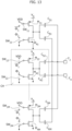
- Figure 13 shows an embodiment based on a combination of the embodiments of Figure 8B and 11 . Specifically, in this embodiment are used M reference capacitances C R1 , C R2 , ... C RM and M sense capacitances C S1 , C S2 , ... C SM .
- a reference capacitance C R and a sense capacitance Cs are connected to a respective half-bridge.
- a first terminal of each sense capacitance C S1 , C S2 , ... C SM is connected ( e.g ., directly) to the node T 2 and the second terminal of each sense capacitance C S1 , C S2 , ... C SM is connected ( e.g ., directly) to the intermediate node of the respective half-bridge formed by two electronic switches, i.e ., half-bridges formed by two electronic switches M 21 and M 41 , two electronic switches M 22 and M 42 , etc.
- each reference capacitance C R1 , C R2 , ... C RM is connected ( e.g ., directly) to the node T 4 and the second terminal of each reference capacitance C R1 , C R2 , ... C RM is connected ( e.g ., directly) to the intermediate node of the respective half-bridge.
- the measurement system comprises M half-bridges, one for each channel CH comprising a respective reference capacitance C R and a respective sense capacitance Cs.
- each high-side electronic switch M 21 , ... M 2M has associated a respective electronic switch SW 11 , SW 12 , ... SW 1M configured to connect the respective gate terminal to the high logic level or the signal ⁇ 1
- each low-side electronic switch M 41 , ... M 4M has associated a respective electronic switch SW 21 , SW 22 , ... SW 2M configured to connect the respective gate terminal to the low logic level or the signal ⁇ 2
- the control signal for the electronic switches SW 11 , SW 12 , ... SW 1M and SW 21 , SW 22 , ... SW 2M may be generated by the control circuit 36a or the processing circuit 44 (not shown in Figure 13 ).
- the measurement system has now a rather symmetric capacitive load.
- the measurement system has a large loading on the input terminals of the operational amplifier 3440.
- Figure 14 shows thus a slightly different embodiment.
- a reference capacitance C R and a sense capacitance Cs are again connected to a respective half-bridge.
- a first terminal of each sense capacitance C S1 , C S2 , ... C SM is connected ( e.g ., directly) to the intermediate node of the respective half-bridge formed by two electronic switches, i.e ., half-bridges formed by two electronic switches M 21 and M 41 , two electronic switches M 22 and M 42 , etc.
- the second terminal of each sense capacitance C S1 , C S2 , ... C SM is connected ( e.g ., directly) via a respective electronic switch SW 11 , SW 12 , ... SW 1M to the node Tz.
- each reference capacitance C R1 , C R2 , ... C RM is connected ( e.g ., directly) to the intermediate node of the respective half-bridge and the second terminal of each reference capacitance C R1 , C R2 , ... C RM is connected (e.g., directly) via a respective electronic switch SW 21 , SW 22 , ... SW 2M to the node T 2 .
- the electronic switches SW 11 , SW 12 , ... SW 1M and SW 21 , SW 22 , ... SW 2M may be driven via respective control signals in order to connect a single sense capacitance C S1 , C S2 , ... C SM and a single reference capacitance C R1 , C R2 , ... C RM to the respective half-bridge.
- the control signals may be generated by the control circuit 36a or the processing circuit 44 (not shown in Figure 14 ).
- the embodiments shown in Figure 11 and 12 may also be combined, i.e ., the measurement system may comprise electronic switches for selectively connecting the control terminals of the electronic switches M 21 , M 41 , ... M 2M , M 4M to the signals ⁇ 1 and ⁇ 2 (as shown in Figures 11 and 13 ) and electronic switches for selectively connecting the sense capacitances to the node T 2 (as shown in Figures 12 and 14 ).
- the measurement system may also comprise electronic switches for selectively connecting the reference capacitances to the node T 4 (as shown in Figure 14 ).
- the measurement system 34a disclosed herein may be used to monitor a different charge injected into two capacitances C 1 and C 2 , which in turn may be indicative of a different capacitance value of the two capacitances C 1 and C 2 or a different voltage V 1 and V 2 used to charge the capacitances C 1 and C 2 .
- the measurement system may be used to detect the presence of a sample material across an integrated capacitor in a very accurate way.
- the sensitivity of the measurement system is mainly determined by the mismatch between the reference and the sensing capacitors.
- the detection is very fast.
- the asynchronous detection based on an asynchronous reset via the signal S permits to further increase the speed of the system.
Landscapes
- Engineering & Computer Science (AREA)
- Power Engineering (AREA)
- Physics & Mathematics (AREA)
- General Physics & Mathematics (AREA)
- Measurement Of Resistance Or Impedance (AREA)
Abstract
Description
- The embodiments of the present description refer measurement systems, such as capacitive sensors.
- Capacitive sensors are commonly used. For example, such capacitive sensor may have a high resolution, low complexity and low temperature-dependency. For example, such capacitive sensors may be used in microelectromechanical systems (MEMS) based sensors, such as accelerometers, position sensors, pressure sensors, and moisture sensors. Recently, such capacitive sensors have also been used for Laboratory on a Chip (LoC) applications, e.g., for DNA protein interaction quantification, cellular monitoring, bio-particle detection, organic solvent monitoring, sensing of droplet parameters, bacteria detection, etc.
- In general, a capacitive sensor comprises at least one couple of sensing electrodes that are connected to an interface readout circuit.
- For example,
Figure 1 shows a typical LoC application, wherein twoelectrodes circuit 20. In a capacitive sensor, theelectrodes circuit 20, which is configured to generate an analog or digital signal by measuring a value being indicative of the capacitance value between theelectrodes - Accordingly, in case the physical, biological and/or chemical properties of a
sample 104 in the vicinity of theelectrodes electrodes circuit 20, may be configured to provide an estimate of the physical, biological and/or chemical properties of thesample 104 as a function of the measured capacitance value. - In this respect the Complementary Metal-Oxide-Semiconductor (CMOS) technology offers great advantages for the development of capacitive sensors, e.g., because it permits to implement highly integrated circuits with low costs. This permits also to achieve a higher sensitivity and a rapid detection, and to integrate the electrical readout circuit and/or the sensing electrodes on a
single chip 20. Those of skill in the art will appreciate that various CMOS capacitive sensing techniques have been proposed in literature for different LoC applications. One of the most commonly used technique is the charge-based capacitance measurement (CBCM). For example, the CBCM technique is described in document James C. Chen, Bruce W. McGaughy, Dennis Sylvester, and Chenming Hu, "An On-Chip, Attofarad Interconnect Charge-Based Capacitance Measurement (CBCM) Technique", International Electron Devices Meeting (IEDM) 1996, or United States Patent Application n.US 2003/0218473 A1 , which are incorporated herein by reference. -
Figure 2 shows an example of aninterface circuit 30 according to the CBCM technique. - As mentioned before, the
electrodes sample 104 in the vicinity of theelectrodes - Specifically, in the example considered, the current path of a first electronic switch M4, such as a transistor, such as an n-channel Field-effect transistor (FET), such as an n-channel Metal-Oxide-Semiconductor (MOS) FET, is connected (e.g., directly) in parallel with the sense capacitance Cs, i.e., the electronic switch M4 is connected between the
electrodes - Moreover, the interface circuit comprises a second electronic switch M2, such as a transistor, such as an p-channel Field-effect transistor (FET), such as an p-channel MOSFET, configured to selectively connect the sense capacitance Cs to a supply voltage VDD as a function of a control signal Φ1 received at a control terminal of the electronic switch M2, e.g., the gate terminal of a corresponding FET. For example, in the example considered, the
electrode 102 of the capacitance Cs is connected to a first reference voltage, e.g., ground GND, and theelectrode 100 is connected via the electronic switch M2 to a second reference voltage, e.g., a supply voltage VDD of theintegrated circuit 20. Accordingly, when the electronic switch M4 is opened, the electronic switch M2 may be used to selectively charge the sense capacitance Cs. Accordingly, acontrol circuit 36 may be configured to generate the control signals Φ1 and Φ2 in order to selectively charge and discharge the sense capacitance Cs. - For example, as shown in
Figure 3 , typically, thecontrol circuit 36 is configured to generate the control signals Φ1 and Φ2 according to switching cycles having a duration/period TS. Specifically, typically, each switching cycle TS comprises a sequence of the following four phases: - a phase Δt1, wherein both electronic switches M2 and M4 are opened, e.g., by setting the signal Φ1 to high and the signal Φ2 to low;
- a phase Δt2, wherein the electronic switch M2 is opened and the electronic switch M4 is closed, e.g., by setting the signal Φ1 to high and the signal Φ2 to high, whereby the capacitance Cs discharges trough the electronic switch M4 to ground;
- a phase Δt3, wherein both electronic switches M2 and M4 are opened, e.g., by setting the signal Φ1 to high and the signal Φ2 to low; and
- a phase Δt4, wherein the electronic switch M2 is closed and the electronic switch M4 is opened, e.g., by setting the signal Φ1 to low and the signal Φ2 to low, whereby the sense capacitance Cs is connected to the supply voltage VDD and is charged with a current is.
- Accordingly, the phase Δt2 is used to reset the charge of the capacitance Cs and the phase Δt4 is used to charge the capacitance Cs. Generally, the phases Δt1 and Δt3 are purely optional and are used to avoid that the electronic switches M2 and M4 generate a short-circuit by connecting the supply voltage VDD to ground.
- Accordingly, as shown in
Figure 2 , theinterface circuit 30 may comprise ameasurement circuit 34 configured to measure the charge or discharge current is flowing through the capacitance Cs. For example, in the example considered, themeasurement circuit 34 comprises acurrent sensor 340 connected between the electronic switch M2 and the supply voltage VDD, thereby monitoring the charge current. - Typically, the CBCM technique uses also a second branch, which comprises a reference capacitance CR. Typically, the reference capacitance CR has the same physical structure as the sense capacitance CS, but is not exposed to the
sample 104. For example, in the absence of asample 104, the capacitance values Cs and CR typically correspond, i.e., Cs = CR. Conversely, in the presence of asample 104, the capacitance value of the sense capacitance Cs varies and usually increases, i.e., Cs > CR. - Accordingly, in this case, the second branch comprises:
- a first electronic switch M3, such as an n-channel FET, such as a n-channel MOSFET, configured to selectively short-circuit the reference capacitance CR, and
- a second electronic switch M1, such as a p-channel FET, such as a p-channel MOSFET, configured to selectively connect the reference capacitance CR to the supply voltage VDD.
- Typically, the electronic switch M3 is driven via the control signal Φ2 and the electronic switch M1 is driven via the control signal Φ1. In fact, as shown in
Figure 3 , in this case the reference capacitance CR is reset during the phase Δt2 and is charged during the phase Δt4, thereby generating a current flow iR. Accordingly, also in this case theinterface circuit 30 may comprise acurrent sensor 342 configured to measure the charge or discharge current iR flowing through the capacitance CR. For example, in the embodiment considered, thecurrent sensor 342 is connected between the electronic switch M1 and the supply voltage VDD, thereby monitoring the charge current. - Accordingly, in the example considered, the
interface circuit 30 comprises a first half-bridge implemented with the electronic switches M2 and M4, wherein the first half-bridge is configured to selectively apply a first reference voltage (usually the supply voltage VDD) or a second reference voltage (usually ground GND) to a first terminal/electrode 100 of the sense capacitance Cs, wherein the second terminal/electrode 102 of the sense capacitance Cs is connected to the second reference voltage (usually ground GND). Moreover, theinterface circuit 30 comprises a second half-bridge implemented with the electronic switches M1 and M3, wherein the second half-bridge is configured to selectively apply the first reference voltage (usually the supply voltage VDD) or the second reference voltage (usually ground GND) to a first terminal/electrode of the reference capacitance CR wherein the second terminal/electrode of the reference capacitance CR is connected to the second reference voltage (usually ground GND). The two half-bridges are identified asCBCM cell 32. - For example, when using the CMOS technology, the electronic switches M3 and M4 are usually implemented with n-channel MOSFETs and the electronic switches M1 and M2 are usually implemented with p-channel MOSFETs. In this case, the source terminals of the n-channel FETs M3 and M4 are connected to the second reference voltage (e.g., ground GND), the source terminals of the p-channel FETs M1 and M2 are connected to the first reference voltage (e.g., VDD), the drain terminals of the n-channel FET M4 and the p-channel FET M2 are connected to the first terminal/electrode of the sense capacitance Cs, and the drain terminals of the n-channel FET M3 and the p-channel FET M1 are connected to the first terminal/electrode of the reference capacitance CR.
- Accordingly, in the CBMS technique, the properties of the
sample 104 are usually evaluated based on the capacitive difference ΔC between the capacitances Cs and CR, i.e., ΔC = Cs - CR. For example, for this purpose, themeasurement circuit 32 should be configured to generate a signal indicative of the difference Δi between the (charge or discharge) currents is and iR, i.e., Δi = iS - iR. - In this respect, the previously cited document by James C. Chen affirms that this technique has an intrinsic estimated sensitivity of about 10aF. Accordingly, a major technical problem resides in the design and implementation of the measurement/readout circuit of the
CBCM cell 32 that does not degrade or has only a minor impact on this performance. -
Figure 4 shows a first example of a measurement circuit of theCBCM cell 32 configured to generate a signal indicative of the difference Δi between the currents is and iR. For example, such a solution is disclosed in Saghi Forouhi, Rasoul Dehghani, and Ebrahim Ghafar-Zadeh, "Toward High Throughput Core-CBCM CMOS Capacitive Sensors for Life Science Applications: A Novel Current Mode for High Dynamic Range Circuitry", Sensors 2018. - Specifically, in the example considered, the measurement circuit of the
CBCM cell 32 comprises a firstcurrent mirror 3400, e.g., implemented with two p-channel FETs, configured to generate a current is' by mirroring the (charge) current is provided to theCBCM cell 32. This mirrored current is' is used to charge a first capacitance Cint+, which essentially operates as an integrator configured to convert the current is'(t) into a voltage. Similarly, the measurement circuit of theCBCM cell 32 comprises a secondcurrent mirror 3410, e.g., implemented with two p-channel FETs, configured to generate a current iR' by mirroring the (charge) current iR provided to theCBCM cell 32. This mirrored current iR' is used to charge a second capacitance Cint-, which essentially operates as an integrator configured to convert the current iR'(t) into a voltage. - Accordingly, in the example considered, a
differential amplifier 3420 may be used to generate a signal, e.g., a voltage Vout, by amplifying the difference between the voltage at the capacitance Cint+ and the voltage at the capacitance Cint-. For example, in the example considered, the voltage at the capacitance Cint+ is connected to the positive input terminal of thedifferential amplifier 3420 and the voltage at the capacitance Cint- is connected to the negative input terminal of thedifferential amplifier 3420. The capacitances Cint+ and Cint- have the same capacitance value. - In this case, usually the
measurement circuit 34 also compriseselectronic switches Figure 4 permits to execute a plurality of the switching cycles TS shown inFigure 3 , whereby each time the current pulse in the currents is and iR are transferred to the capacitances Cint+ and Cint-, respectively. - Accordingly, in the example considered, the capacitances Cs and CR are not charged directly with voltage VDD, but rather with a voltage (VDD - Vthp), where Vthp corresponds to the threshold of the input FETs of the
current mirrors differential amplifier 3420 may be approximated with the following equation after a given number N of switching cycles:
- Accordingly, a first drawback relates to the fact the output Vout is also a function of the threshold Vthp, which depends on temperature and process spread variations. Moreover, in this approach, to achieve a higher sensitivity, high voltages across the integrating capacitors Cint+ and Cint- are required. However, this situation may push the
differential amplifier 3420 to a nonlinear region, and thus limits the resolution of the sensor circuit. To mitigate this second problem, the previously cited article by Saghi Forouhi also discloses an alternative approach, which is shown inFigure 5 . - Specifically, in the example shown in
Figure 5 , thecurrent mirrors - However, in this case a further
current mirror 3430, e.g., implemented with n-channel FETs, is used to generate a further mirrored current iR" by mirroring the current iR'. Specifically, in the example considered, the output of thecurrent mirror 3400 is connected in series with a capacitance Cint. Conversely, the output of thecurrent mirror 3430 is connected in parallel with the capacitance Cint. Accordingly, in the example considered, the capacitance Cint is indeed charged with a current ix corresponding to the difference between the currents is' and in", i.e., ix = is' - iR". - Accordingly, also the circuit of
Figure 5 permits to execute a plurality of the switching cycles shown inFigure 3 , whereby each time the current pulse in the current ix is transferred to the capacitances Cint. Specifically, by using acurrent mirror 3430 with a mirroring ratio of one, andcurrent mirrors 
- Generally, the previously cited document also discloses a respective differential version of the circuit shown in
Figure 5 . - Unfortunately, the approach shown in
Figure 5 is based on several current mirrors having current gains, whose offsets and mismatches severely impact the sensing of the capacitance difference ΔC. Conversely, this was only a minor problem in the solution shown inFigure 4 , because current mirrors without any gain may be used. - Considering the foregoing, it is therefore an object of various embodiments to provide a measurement system, which overcomes the problems outlined in the foregoing.
- According to one or more embodiments, the above object is achieved by a measurement system having the distinctive elements set forth specifically in the ensuing claims. Embodiments moreover concern a related integrated circuit and method.
- The claims form an integral part of the technical teaching of the description provided herein.
- As mentioned before, various embodiments of the present disclosure relate to a measurement system. In various embodiments, the measurement system comprises a first capacitance and a second capacitance. The measurement system comprises moreover a switching circuit configured to receive a first and a second control signal. In response to determining that the first control signal is asserted, the switching circuit connects a first terminal of the first capacitance to a first voltage and a first terminal of the second capacitance to a second voltage. Moreover, in response to determining that the second control signal is asserted, the switching circuit connects the first terminal of the first capacitance and the first terminal of the second capacitance to a reference voltage, e.g., ground.
- In various embodiments, a control circuit is configured to generate the first and the second control signal according to switching cycles comprising four intervals. Specifically, for a first interval, the control circuit de-asserts the first and the second control signal. For a following second interval, the control circuit de-asserts the first control signal and asserts the second control signal, thereby connecting the first capacitance to the first voltage and the second capacitance to the second voltage. For a following third interval, the control circuit de-asserts the first and the second control signal. Finally, for a following fourth interval, the control circuit asserts the first control signal and de-asserts the second control signal, thereby connecting the first capacitance and the second capacitance to the reference voltage.
- In various embodiments, the measurement system comprises further a measurement circuit, which in turn comprises a differential integrator and a comparator with hysteresis.
- In various embodiments, the differential integrator comprises a differential operational amplifier, a first integration capacitance and a second integration capacitance. Specifically, in various embodiments, an inverting input of the differential operational amplifier is connected to a second terminal of the first capacitance and a non-inverting input of the differential operational amplifier is connected to a second terminal of the second capacitance. A first terminal of the first integration capacitance is connected to the inverting input of the differential operational amplifier and a second terminal of the first integration capacitance is connected via a first electronic switch to a positive output terminal of the differential operational amplifier, wherein the second terminal of the first integration capacitance represents a first output node of the differential integrator. Similarly, a first terminal of the second integration capacitance is connected to the non-inverting input of the differential operational amplifier and a second terminal of the second integration capacitance is connected via a second electronic switch to a negative output terminal of the differential operational amplifier, wherein the second terminal of the second integration capacitance represents a second output node of the differential integrator. In various embodiments, the differential integrator comprises moreover a third electronic switch connected between the inverting input of the differential operational amplifier and the positive output terminal of the operational amplifier, and a fourth electronic switch connected between the non-inverting input of the differential operational amplifier and the negative output terminal of the operational amplifier.
- In various embodiments, the comparator with hysteresis is configured to, in response to determining that a voltage applied to a negative input terminal of the comparator with hysteresis exceeds a voltage applied to a positive input terminal of the comparator with hysteresis plus a hysteresis threshold, set a first output terminal of the comparator with hysteresis to high and a second output terminal of the comparator with hysteresis to low. Moreover, in various embodiments the comparator with hysteresis comprises a fifth electronic switch connected between the negative input of the comparator with hysteresis and the second output terminal of the comparator with hysteresis, and a sixth electronic switch connected between the positive input of the comparator with hysteresis and the first output terminal of the comparator with hysteresis.
- In various embodiments, a first decoupling capacitance is connected between the negative input of the comparator with hysteresis and the first output node of the differential integrator, and a second decoupling capacitance connected between the positive input of the comparator with hysteresis and the second output node of the differential integrator.
- In various embodiments, the measurement system is configured to manage a normal operation phase and a reset phase.
- Specifically, during the normal operation phase, the measurement system is configured to close the first electronic switch and the second electronic switch, in response to determining that the second control signal is asserted. Conversely, the measurement system is configured to open the first electronic switch and the second electronic switch in response to determining that the second control signal is de-asserted. Moreover, the measurement system is configured to close the third electronic switch and the fourth electronic switch in response to determining that the first control signal is asserted, and open the third electronic switch and the fourth electronic switch in response to determining that the first control signal is de-asserted. Thus, when the first control signal is de-asserted and the second control signal is asserted, the first integration capacitance and the second integration capacitance are connected into the feedback paths of the differential operational amplifier, thereby permitting a charge transfer from the first and second capacitances to the first and second integration capacitances. For example, the first and the second capacitances have a different charge when the first voltage and the second voltage correspond to a common voltage, but the first capacitance corresponds to a sense capacitance and the second capacitance corresponds to a reference capacitance. In fact, in this case, the voltage between the first and second output nodes of the differential integrator is indicative of the difference between the capacitances of the sense capacitance and the reference capacitance. Conversely, when the first capacitance and the second capacitance have the same capacitance value, the voltage between the first and second output nodes of the differential integrator is indicative of the difference between the first voltage and the second voltage. During the normal operation phase, the comparator with hysteresis is thus operative, i.e., the fifth electronic switch and the sixth electronic switch are opened.
- In various embodiments, the measurement system monitors also a reset request signal during the normal operation phase and, in response to determining that the reset request signal indicates a reset request, the measurement system starts the reset phase. For example, in various embodiments, the measurement system is configured to assert the reset request signal after a given maximum number of the switching cycles, and/or in response to determining that the first output terminal of the comparator with hysteresis is set to high and/or the second output terminal of the comparator with hysteresis is set to low.
- In various embodiments, during the reset phase, the measurement system executes one or more sub-phases. Specifically, for a first reset interval, the measurement system closes the first, second, third, fourth, fifth and sixth electronic switches. Conversely, for a following second reset interval, the measurement system may open the third and fourth electronic switches and keeps closed the first, second, fifth and sixth electronic switches. Finally, at the end of the reset phase, e.g., at the end of second phase, the measurement system starts again the normal operation phase. Specifically, as will be described in greater detail in the following, in various embodiments, apart from resetting the integration capacitances and the comparator with hysteresis, the offsets and most of the flicker noise of the differential operational amplifier and the comparator with hysteresis may be stored to the decoupling capacitance during the first reset interval. Moreover, during the second reset interval, also the charge-injection and clock-feedthrough of the third and fourth electronic switches may be stored to the decoupling capacitance.
- For example, in order to implement the described reset phase, the differential integrator may receive a first reset signal, and the third electronic switch and the fourth electronic switch may be configured to be closed in response to determining that the first control signal is asserted or the first reset signal is asserted. Moreover, the comparator with hysteresis may be configured to receive a second reset signal, wherein the fifth electronic switch and the sixth electronic switch are configured to be closed in response to determining that the second reset signal is asserted. Accordingly, in this case, the measurement system may be configured to, while the control circuit asserts the second control signal, assert the first reset signal and the second reset signal for the first reset interval, and de-assert the first reset signal and assert the second reset signal for the second reset interval. For example, for this purpose the measurement system may comprise a delay circuit configured to generate the second reset signal by delaying the first reset signal.
- Accordingly, various embodiments relate to a corresponding method of operating such a measurement system. Specifically, during a normal operation phase, the method closes the first electronic switch and the second electronic switch in response to determining that the second control signal is asserted, and opens the first electronic switch and the second electronic switch in response to determining that the second control signal is de-asserted. Moreover, the method closes the third electronic switch and the fourth electronic switch in response to determining that the first control signal is asserted, and opens the third electronic switch and the fourth electronic switch in response to determining that the first control signal is de-asserted. In various embodiments, when using the fifth electronic switch and the sixth electronic switch, the method may also open the fifth electronic switch and the sixth electronic switch during a normal operation phase.
- In various embodiments, the method may monitor a reset request signal indicating a reset request and start a reset phase in response to determining that the reset request signal indicates a reset request. Specifically, during the reset phase, the method closes the first, second, third, fourth electronic switches for a first reset interval. Moreover, when using the fifth and sixth electronic switches, the method may close the fifth and sixth electronic switches. Preferably, in this case, the measurement system comprises the decoupling capacitances. Next, the method starts again the normal operation phase.
- In various embodiments, when using the decoupling capacitances, the method may also open the third and fourth electronic switches and keep closed the first, second, fifth and sixth electronic switches for a following second reset interval following the first reset interval (and before the normal operation mode is started again).
- The embodiments of the present disclosure will now be described with reference to the annexed plates of drawings, which are provided purely to way of non-limiting example and in which:
The features and advantages of the present invention will become apparent from the following detailed description of practical embodiments thereof, shown by way of non-limiting example in the accompanying drawings, in which: -
Figure 1 shows an example of a capacitive sensor; -
Figures 2 shows an example of a measurement system for capacitive sensors; -
Figure 3 shows waveforms of the measurement system ofFigure 2 ; -
Figures 4 and5 show possible implementations of the measurement system ofFigure 2 ; -
Figure 6 shows an embodiment of a measurement system according to the present disclosure; -
Figure 7 shows an embodiment of a measurement circuit of the measurement system ofFigure 6 ; -
Figures 8A, 8B and 8C show embodiments of switching circuits of the measurement system ofFigure 6 ; -
Figure 9 shows an embodiment of waveforms of the measurement system ofFigure 6 ; -
Figure 10 shows a detail of the measurement circuit ofFigure 7 ; and -
Figures 11 ,12 ,13 and14 show further embodiments of switching circuits of the measurement system ofFigure 6 . - In the ensuing description, various specific details are illustrated aimed at enabling an in-depth understanding of the embodiments. The embodiments may be provided without one or more of the specific details, or with other methods, components, materials, etc. In other cases, known structures, materials, or operations are not shown or described in detail so that various aspects of the embodiments will not be obscured.
- Reference to "an embodiment" or "one embodiment" in the framework of this description is meant to indicate that a particular configuration, structure, or characteristic described in relation to the embodiment is comprised in at least one embodiment. Hence, phrases such as "in an embodiment", "in one embodiment", or the like that may be present in various points of this description do not necessarily refer to one and the same embodiment. Moreover, particular conformations, structures, or characteristics may be combined in any adequate way in one or more embodiments.
- The references used herein are only provided for convenience and hence do not define the sphere of protection or the scope of the embodiments.
- In
Figures 6 to 14 described below, parts, elements or components that have already been described with reference toFigures 1 to 5 are designated by the same references used previously in these figures. The description of these elements has already been made and will not be repeated in what follows in order not to burden the present detailed description. - As mentioned before, various embodiments of the present disclosure relate to a measurement system.
-
Figure 6 shows an embodiment of a measurement system according to the present disclosure. For example, such a measurement system may be integrated in anintegrated circuit 40. In the embodiment considered, the measurement system comprises aswitching circuit 32a comprising three terminals: - a first terminal configured to be connected to a reference voltage Vref, such as ground GND;
- a second terminal configured to be connected to a first voltage V1, wherein the first voltage is greater than the reference voltage Vref/ground GND; and
- a third terminal configured to be connected to a second voltage V2, wherein the second voltage is greater than the reference voltage Vref/ground GND.
- As will be described in greater detail in the following, in various embodiments, the voltages V1 and V2 may also correspond to the same voltage, indicated in the following as voltage VA. For example, in various embodiments, the measurement system may comprise a
voltage generator 42 configured to receive a supply voltage VDD, e.g., via a pad/pin of theintegrated circuit 40, and generate the voltage VA based on this supply voltage VDD. - In the embodiment considered, the measurement system has associated two capacitances C1 and C2. These capacitances are preferably integrated in the measurement system for best matching. In general, the capacitance has two terminals T1 and T2, and the capacitance has two terminals T3 and T4.
- Specifically, in various embodiments, the switching
circuit 32a receives a first control signal Φ1 and a secondo control signal Φ2. For example, the control signal Φ1 and Φ2 may be generated by acontrol circuit 36a of the measurement system. Specifically, similar to the previous description, thecontrol circuit 36a may be configured to generate the control signals Φ1 and Φ2 according to switching cycles having a duration/period Ts, wherein each switching cycle TS comprises a sequence of the following four phases: - a phase Δt1, wherein the signals Φ1 and Φ2 are de-asserted;
- a phase Δt2, wherein the signal Φ1 is de-asserted and the signal Φ2 is asserted;
- a phase Δt3, wherein the signals Φ1 and Φ2 are de-asserted;
- a phase Δt4, wherein the signal Φ1 is asserted and the signal Φ2 is de-asserted;
- For example, in various embodiments, the switching
circuit 32a is configured to: - in response to determining that the signal Φ1 is asserted and the signal Φ2 is de-asserted, connect the terminal T1 to the voltage V1 and the terminal T3 to the voltage V2;
- in response to determining that the signal Φ1 is de-asserted and the signal Φ2 is asserted, connect the terminals T1 and T3 to the reference voltage Vref/ground GND; and
- in response to determining that the signals Φ1 and Φ2 are de-asserted, put the terminals T1 and T3 in a high-impedance state, e.g., by disconnecting the terminals T1 and T3.
- Accordingly, in various embodiments, the switching
circuit 32a is configured to apply the reference voltage Vref, or the voltages V1 and V2, to the terminals T1 and T3 of the capacitances C1 and C2, respectively. - Accordingly, in various embodiments, a
measurement circuit 34a is configured to monitor a current i1 flowing through the capacitance C1 and a current i2 flowing through the capacitance C2. -
Figure 7 shows an embodiment of ameasurement circuit 34a according to the present disclosure. - Specifically, in the embodiment considered, the
measurement circuit 34a is implemented with a switched capacitor (SC) differential integrator. Specifically, in the embodiment considered, the differential integrator comprises a differentialoperational amplifier 3440, wherein the inverting/negative input terminal of theoperational amplifier 3440 is connected (e.g., directly) to the terminal T2 of the capacitance C1, and the non-inverting/positive input terminal of theoperational amplifier 3440 is connected (e.g., directly) to the terminal T4 of the capacitance C2. Specifically, in order to implement a differential integrator configured to integrate the difference Δi between the currents i1 and i2 during the discharge phase, i.e., when the signal Φ2 is asserted, the differential integrator comprises: - a first integration capacitance Cn, wherein a first terminal of the integration capacitance CI1 is connected (e.g., directly) to the inverting/negative input terminal of the
operational amplifier 3440 and a second terminal of the first integration capacitance CI1 is connected (e.g., directly) via the current path of anelectronic switch 3448 to the positive output terminal of theoperational amplifier 3440; - a second integration capacitance CI2, wherein a first terminal of the integration capacitance CI2 is connected (e.g., directly) to the non-inverting/positive input terminal of the
operational amplifier 3440 and a second terminal of the second integration capacitance CI2 is connected (e.g., directly) via the current path of anelectronic switch 3450 to the negative output terminal of theoperational amplifier 3440. - Specifically, the
electronic switches electronic switches operation amplifier 3440. In various embodiments, the first and second integration capacitance CI1 and CI2 have the same capacitance CI. For example, the capacitances CI1 and CI2 may be implemented with internal capacitors for best matching with the capacitances C1 and C2. - Moreover, in the embodiment considered, the current path of an
electronic switch 3452 is connected (e.g., directly) between the inverting/negative input terminal of theoperational amplifier 3440 and the positive output terminal of theoperational amplifier 3440, and the current path of anelectronic switch 3454 is connected (e.g., directly) between the non-inverting/positive input terminal of theoperational amplifier 3440 and the negative output terminal of theoperational amplifier 3440. Specifically, theelectronic switches electronic switches operation amplifier 3440. - As schematically shown in
Figure 7 , the differentialoperational amplifier 3440 has also associated a respective common mode voltage VCM, which may be fixed or settable. - Accordingly, when the signal Φ1 is asserted, the input terminals of the
operational amplifier 3440 are set to the common mode voltage VCM, which permits to charge the capacitances C1 and C2 via the voltages V1 and Vz. Conversely, when the signal Φ2 is asserted, the integration capacitances CI1 and CI2 are connected to theoperational amplifier 3440 and the previously charged capacitances C1 and C2 discharge to the reference voltage Vref/ground GND. Specifically, the charge applied to the capacitances C1 and C2 is different, e.g., when: - the voltages V1 and V2 have the same value, e.g., VA, but the capacitances C1 and C2 are different, which thus permits to monitor the difference between the capacitances C1 and C2, or
- the capacitances C1 and C2 have the same value, but the voltages V1 and V2 are different, which thus permits to monitor the difference between the voltages V1 and V2.
- For example,
Figures 8A, 8B and 8C show possible embodiments of theswitching circuit 32a and the capacitances C1 and Cz. - Specifically, in
Figures 8A and 8B , the capacitance C1 corresponds to a sense capacitance Cs and the capacitance C2 corresponds to a reference capacitance CR, i.e., the capacitance Cs has a variable capacitance value. Moreover, in this case, the voltages V1 and V2 are connected to a common voltage VA, which may be provided via a terminal/pad/pin of the measurement system or via thevoltage generator 42. - For example, the switching
circuit 32a ofFigure 8A essentially corresponds to the switchingcircuit 32 shown inFigure 2 . Specifically, in the embodiment considered, the current path of a first electronic switch M4, such as a transistor, such as an n-channel FET, such as an n-channel MOSFET, is connected (e.g., directly) between the terminal T1 and the reference voltage Vref/ground GND. Moreover, the current path of a second electronic switch M2, such as a transistor, such as an p-channel Field-effect transistor (FET), such as an p-channel MOSFET, is connected (e.g., directly) between the terminal T1 and the voltage VA. Similarly, the current path of a third electronic switch M3, such as a transistor, such as an n-channel FET, such as an n-channel MOSFET, is connected (e.g., directly) between the terminal T3 and the reference voltage Vref/ground GND. Moreover, the current path of a fourth electronic switch M1, such as a transistor, such as an p-channel Field-effect transistor (FET), such as an p-channel MOSFET, is connected (e.g., directly) between the terminal T3 and the voltage VA. - For example, when the electronic switches M1 and M2 are implemented with p-channel FETs, the switches M1 and M2 are indeed closed when the signal Φ1 is set to low. Thus, when the
control circuit 36a is configured to assert the signal Φ1 by setting signal Φ1 to high, indeed the inverted signalΦ 1 may be used to drive the gate terminal of the p-channel FETs M1 and M2 (see alsoFigure 8A ). - Accordingly, in the embodiment shown in
Figure 8A , the two half-bridges formed by the switches M1/M3 and M2/M4 indeed operate in parallel based on the same control signals. Accordingly, as shown inFigure 8B , in various embodiments, the electronic switches M1 and M3 may be omitted, and the terminal T3 of the reference capacitance CR may be connected (e.g., directly) to the terminal T1 of the sense capacitance Cs. - Conversely, in
Figure 8C , the capacitances C1 and C2 have the same value Cs. Moreover, the voltages V1 is connected to a voltage Vin+ and the voltages V2 is connected to a voltage Vin-. - Accordingly, also in this case may be used two half-bridges. For example, in the embodiment considered, the current path of a first electronic switch M4, such as a transistor, such as an n-channel FET, such as an n-channel MOSFET, is connected (e.g., directly) between the terminal T1 and the reference voltage Vref/ground GND. Moreover, the current path of a second electronic switch M2, such as a transistor, such as an p-channel Field-effect transistor (FET), such as an p-channel MOSFET, is connected (e.g., directly) between the terminal T1 and the voltage Vin+. Similarly, the current path of a third electronic switch M3, such as a transistor, such as an n-channel FET, such as an n-channel MOSFET, is connected (e.g., directly) between the terminal T3 and the reference voltage Vref/ground GND. Moreover, the current path of a fourth electronic switch M1, such as a transistor, such as an p-channel Field-effect transistor (FET), such as an p-channel MOSFET, is connected (e.g., directly) between the terminal T3 and the voltage Vin-.
- Accordingly, the embodiments shown in
Figures 8A and 8B may be used to monitor the difference ΔC between the capacitances Cs and CR, while the embodiment shown inFigure 8C may be used to monitor the amplitude of a differential voltage ΔVin corresponding to the difference between the voltages Vin+ and Vin-. - For example, when using the
measurement circuit 34a ofFigure 7 with the switchingcircuits 32a shown inFigures 8A and 8B , the following net charge will be injected into the integration capacitances CI1 and CI2 at each switching cycle Ts:
- Accordingly, assuming that the capacitances CI1 and CI2 have the same value CI and when repeating a given number N of switching cycles Ts, the differential output voltage VO,AMP of the
operational amplifier 3440 during the intervals when the signal Φ2 is asserted is given by:
- Conversely, when using the
measurement circuit 34a ofFigure 7 with the switchingcircuits 32a shown inFigure 8C , the capacitances Cs are reset to the common mode voltage VCM when the signal Φ1 is asserted. Conversely, when the signal Φ2 is asserted, a differential voltage ΔVin (between Vin+ and Vin-) is applied to the capacitors Cs, thereby injecting the following net charge at each switching cycle Ts:
- Accordingly, assuming that the capacitances CI1 and CI2 have the same value CI and when repeating a given number N of switching cycles Ts, the differential output voltage VO,AMP of the
operational amplifier 3440 during the intervals when the signal Φ2 is asserted is given by:
- Specifically, when opening the
electronic switches electronic switch 3448, represents a first output terminal OUT+ of the integrator circuit, and the second terminal of the integration capacitance CI2, i.e., the intermediate node between the capacitance CI2 and theelectronic switch 3450, represents a second output terminal OUT-of the integrator circuit, wherein the output terminals OUT+ and OUT- provide a differential voltage VO, e.g., corresponding to the previously indicated voltages VO,AMP. - In various embodiments, the
measurement circuit 34a may be configured to assert a signal S when the voltage VO exceeds a reference threshold within a given monitoring interval, which comprises a given number N of switching/integration cycles Ts, thereby indicating that current difference Δi = i1 - i2 exceeds a given threshold value, which in turn may indicate that the capacitance difference ΔC (e.g.,Figures 8A or 8B ) or the differential voltage ΔVin (e.g.,Figure 8C ) exceeds a respective threshold. For example, the signal S may be provided to a terminal/pad/pin of the measurement system or, as shown inFigure 6 , to a digital and/oranalog processing circuit 44 of the measurement system. For example, theprocessing circuit 44 may be a microprocessor programmed via software instructions. - Specifically, in various embodiments, the signal S is generated via a differential comparator with
hysteresis 3446 configured to assert the signal S when the voltage VO exceeds the hysteresis threshold of thecomparator 3446. - In general, such a comparator with
hysteresis 3446 comprises two input terminals for receiving a differential voltage ΔVCMP and two output terminals form providing signals OUT and OUTN, wherein thecomparator 3446 is configured to set the signal OUT to high and the signal OUTN to low in response to determining that the voltage at the negative input terminal exceeds the voltage at the positive input terminal plus a first hysteresis voltage VH1 of the comparator. Similarly, thecomparator 3446 is configured to set the signal OUT to low and the signal OUTN to high in response to determining that the voltage at the negative input terminal falls below the voltage at the positive input terminal minus a second hysteresis voltage VH2. In various embodiments, the first hysteresis voltage VH1 and the second hysteresis voltage VH2 have the same absolute value VH. - Accordingly, in the embodiment considered, the signal S may correspond, e.g., to the signal OUT. Conversely, in the embodiment considered, the
measurement circuit 34a comprises afirst inverter 3460 configured to generate the signal S by inverting the signal OUTN. In this case, themeasurement circuit 34a comprises preferably also asecond inverter 3462 configured to generate a signal SN by inverting the signal OUT. Specifically, theseinverters hysteresis 3446. In general, theinverters - In the embodiment considered, the input terminals of the
comparator 3446 are not connected directly to the nodes OUT+ and OUT-, but one of the input terminals of thecomparator 3446, e.g., the negative input terminal, is connected (e.g., directly) via a first capacitance/capacitor CDEC1 to the node OUT+ and the other input terminal of thecomparator 3446, e.g., the positive input terminal, is connected (e.g., directly) via a second capacitance/capacitor CDEC2 to the node OUT-. These capacitances CDEC1 and CDEC2 have the same capacitance value CDEC. - On the one hand, these capacitances CDEC1 and CDEC2 represent decoupling capacitances between the integrator and the comparator, which thus only transfer the variations of the voltages at the nodes OUT+ and OUT- to the input terminals of the comparator. However, in various embodiments, also the offsets and most of the flicker noise of the
operational amplifier 3440 and the comparator withhysteresis 3446 may be stored to the capacitances CDEC1 and CDEC2 during a reset phase whereby these voltages are then cancelled during the subsequent sensing operation. - Specifically, in various embodiments, to order to start a new measurement cycle, an asynchronous reset is performed once the signal S is asserted, i.e., the signal S corresponds to a reset signal Reset1.
- In general, the
integrator 3440 may be reset by short-circuiting the integration capacitances CI1 and CI2. For example, inFigure 7 , the integration capacitances CI1 and CI2 are reset, when theelectronic switches electronic switches electronic switches gates - Accordingly, as shown in
Figure 9 , once the signal S is asserted during a given discharge phase Δt4 (when the signal Φ1 is asserted), the reset signal Reset1 is also asserted. Accordingly, at the next charge phase Δt2 (when the signal Φ2 is asserted), the integration capacitances CI1 and CI2 are short-circuited, whereby the integrator is reset. - In various embodiments, also the comparator with
hysteresis 3446 is reset during the reset phase. For example, in various embodiments, thecomparator 3446 is reset by closing anelectronic switch 3464 configured to short-circuit the output terminal OUTN and the negative input terminal of thecomparator 3446 and anelectronic switch 3466 configured to short-circuit the output terminal OUT and the positive input terminal of thecomparator 3446. - In various embodiments, the
electronic switches Figure 7 , theelectronic switches delay circuit 3456, such as a delay line, receiving the reset signal Reset1 as input. For example,Figure 7 shows afirst delay circuit 3456 configured to generate the drive signal of theelectronic switch 3464 by delaying the signal Reset1, and asecond delay circuit 3458 configured to generate the drive signal of theelectronic switch 3466 by delaying the signal Reset1. - Accordingly, as shown in
Figure 9 , when the signal S/Reset1 is asserted and thecontrol circuit 32a asserts at an instant t1 the signal Φ2, the capacitances CI1 and CI2 are discharged and thecomparator 3446 is reset. Accordingly at a following instant t2 the signal S goes to low. However, this falling edge is just propagated to the reset signal Reset2 after a delay tD. Accordingly, for the time tD, the reset signal Reset1 is de-asserted (and similarly the signal Φ1), while the signal Φ2 and the reset signal Reset2 are still asserted. Accordingly, in this condition theelectronic switches - the
electronic switches 3448 connect the capacitance CI1 between the inverting/negative input terminal of theoperational amplifier 3440 and the positive output terminal of theoperational amplifier 3440; - - the
electronic switches 3450 connect the capacitance CI2 between the non-inverting/positive input terminal of theoperational amplifier 3440 and the negative output terminal of theoperational amplifier 3440; - - the
electronic switch 3464 connects the negative input terminal of thecomparator 3446 to the terminal OUTN; and - - the
electronic switch 3466 connects the positive input terminal of thecomparator 3446 to the terminal OUT. - Accordingly, in the embodiment considered, the offsets and most of the flicker noise of the
operational amplifier 3440 and the comparator withhysteresis 3446 are stored to the capacitances CDEC1 and CDEC2 during the interval between the instants t1 and t2. Conversely, when using the optional delay tD, also the charge-injection and clock-feedthrough of theswitches - In this respect, the inventors have observed that the remaining error may in this way be reduced to the mismatch of the charge-injection and clock-feedthrough of the
switches - In this respect, the inventors have observed that a smaller threshold voltage VH1 permits a faster detection, e.g., of the sample passing over the
electrodes switches - Additionally or alternatively to the asynchronous reset triggered by the signal S, the reset of the
measurement circuit 34a may also be managed based on a timeout, which is used to trigger similar reset phases of the integrator and the comparator. In fact, in line with the previous description, in various embodiments, the measurement system comprises a reset circuit configured to execute, in response to a reset request signal indicating a reset request, such as a rising edge of the signal S, a signal indicating that a given maximum number N of switching cycles have been executed, etc., the following phases in sequence: - in an optional first phase, e.g., between the rising edge of the Reset1 signal and instant t1, close the
electronic switches - in a (immediately following) second phase, e.g., between the instants t1 and t2, close the
electronic switches electronic switches - in an optional (immediately following) third phase, e.g., between the instants t2 and t3, open the
electronic switches electronic switches - In various embodiments, in order to absorb the differential charge injection of the feedback switches 3448 and 3450 driven by Φ2 in presence of a differential signal at the output terminals of the
operational amplifier 3440, these switches may be equipped with dummy switches and/or capacitor Cx is added. - For example, in the embodiment shown in
Figure 7 , a first capacitor CX1 is connected (e.g., directly) between the terminal OUT+ and a reference voltage, such as ground GND, and a second capacitor CX2 is connected (e.g., directly) between the terminal OUT- and the reference voltage, such as ground GND. The capacitors CX1 and CX2 have the same capacitance value. - Conversely,
Figure 10 shows a possible implementation of each of theswitches - Specifically, in the embodiment considered, a first terminal of a respective integration capacitance CI1 or CI2, indicated generically as CI in
Figure 10 , is connected to a respective input terminal of theoperational amplifier 3440 and theelectronic switch 3448/3450 is connected between the second terminal of the respective integration capacitance CI and a respective output node of theoperational amplifier 3440, wherein the intermediate node between the integration capacitance CI and theelectronic switch 3448/3450 corresponds to an output node OUT+ or OUT- of the integrator, generically indicated as node OUT. As mentioned before, optionally a capacitor CX1 or CX2, generically indicated as capacitor Cx inFigure 10 , may be connected between the output node OUT and a reference voltage, e.g., ground GND. - Specifically, in the embodiment considered, each
electronic switch 3448/3450 is implemented with a series connection of two FETs Q1 and Q2, such as n-channel FETs. Specifically, the first FET Q1 is driven via the signal Φ2. Conversely, the second FET Q2 is a dummy switch, wherein the source and drain terminals of the FET Q2 are short-circuited. Moreover, the gate terminal of the FET Q2 is driven via a signal being asserted when the signal Φ2 is de-asserted, such as the inverted version of the signal Φ2 or preferably the signal Φ1. Preferably, the FET Q1 has a given size ratio W1/L1 (channel width/length), and the FET has a ratio W2/L2 corresponding to 0.5 W1/L1. Generally, such dummy switches Q2 for reducing the charge injection are well-known. - Accordingly the solutions described in the foregoing have the advantage that the voltage VO,AMP and similarly VO is not sensitive to process parameters, such as the MOS voltage threshold of the current mirrors of the prior-art solution. Moreover, the voltages V1 and V2 may be external or internal voltages. For example, the voltage VA may correspond to a supply voltage VDD of the
integrated circuit 40 or a reference voltage provided by thevoltage reference 42. Specifically, when using aninternal voltage reference 42 configured to generate the voltage VA, also the threshold value VH1 (and optionally VH2) may be proportional the voltage VA, thereby permitting a tracking of variation of the voltage VA variations. Conversely, a higher sensitivity can be achieved when using the (greater) supply voltage VDD. - For example, in various embodiment, the integration capacitances CI1 and CI2 have a capacitance value of 0.1 pF, the period of a switching cycle TS is 1 µs, the voltage VA has a value of 2.5 V, and the comparison threshold VH1 (and optionally VH2) is 5 mV. For example, assuming a capacitance difference ΔC of 10 aF, the voltage VO reaches the comparison threshold VH1 after N = 20 switching cycles TS. Thus, in this example, the measurement system is able to detect the presence or absence of a sample, such as a sample with small radius crossing the plates of capacitor Cs, producing a change ΔC of 10 aF in approximately 20 µs. Conversely, assuming a capacitance difference ΔC of 40 aF, the voltage VO reaches the comparison threshold VH1 after N = 5 switching cycles Ts, i.e., the measurement system is able to detect the presence or absence of a sample producing a change ΔC of 40 aF in approximately 5 µs.
- In general, the
measurement circuit 34a disclosed in the foregoing may also be used with a plurality of capacitive sensors. For example, such capacitive sensors may form part of a capacitive touch sensor, such as a touch screen. - For example,
Figure 11 shows an embodiment, wherein a single reference capacitance CR and a given number M of sense capacitances CS1, CS2, ... CSM are used. - Specifically, similar to
Figure 8A , a first terminal of the reference capacitance CR is again connected (e.g., directly) to the node T4 connected to themeasurement circuit 34a and the second terminal of the reference capacitance CR is again connected (e.g., directly) to the intermediate node of the half-bridge formed by the electronic switches M1 and M3. Conversely, a first terminal of each sense capacitance CS1, CS2, ... CSM is connected (e.g., directly) to the node T2 connected to themeasurement circuit 34a and the second terminal of each sense capacitance CS1, CS2, ... CSM is connected (e.g., directly) to the intermediate node of a respective half-bridge formed by a high-side switch and a low-side switch electronic switches, i.e., half-bridges formed by two electronic switches M2, and M41, two electronic switches M22 and M42, etc. Specifically, in the embodiment considered, the various half-bridges are configured to connect the respective intermediate node via a respective high-side switch to the voltage VA and via the respective low-side switch to the reference voltage Vref/ground GND. Accordingly, in the embodiment considered, the measurement system comprises a single half-bridge for the reference capacitance CR and a respective half-bridge for each of the M sense capacitances CS1, CS2, ... CSM. - Specifically, in order to select a given channel CH, the control terminal of the electronic switches M21, M41, ... M2M, M4M are selectively connected to the control signals Φ1 and Φ2. For example, assuming that the high-side electronic switches M21, ... M2M are p-channel FETs and the low-side electronic switches M41, ... M4M are n-channel FETs, a given channel CH may be:
- enabled by connecting the gate terminal of the respective high-side electronic switch M21, ... M2M to the signal
Φ 1 and the gate terminal of the respective low-side electronic switch M41, ... M4M to the signal Φ2; and - disabled by connecting the gate terminal of the respective high-side electronic switch M21, ... M2M to a high logic level, such as the supply voltage VDD, and the gate terminal of the respective low-side electronic switch M41, ... M4M to a low logic level, such as ground GND.
- For example, for this purpose, each high-side electronic switch M21, ... M2M has associated a respective electronic switch SW11, SW12, ... SW1M configured to connect the respective gate terminal to the high logic level or the signal
Φ 1, and each low-side electronic switch M41, ... M4M has associated a respective electronic switch SW21, SW22, ... SW2M configured to connect the respective gate terminal to the low logic level or the signal Φ2. For example, the control signal for the electronic switches SW11, SW12, ... SW1M and SW21, SW22, ... SW2M may be generated by thecontrol circuit 36a or the processing circuit 44 (not shown inFigure 11 ). Accordingly, in the embodiment considered, only one of the sense capacitances is usually connected to the terminal T2. - While this embodiment permits to use a single reference capacitance CR, a large loading is applied to the node T2 (e.g., the negative input terminal of the operational amplifier 3440), and a strong capacitive asymmetry is generated between the nodes T2 and T4 (the input terminals of the amplifier 3440).
-
Figure 12 shows thus a slightly different embodiment. - In the embodiment considered, similar to
Figure 11 , a first terminal of the reference capacitance CR is again connected (e.g., directly) to the node T4 and the second terminal of the reference capacitance CR is again connected (e.g., directly) to the intermediate node of the half-bridge formed by the electronic switches M1 and M3. However, this time a first terminal of each sense capacitance CS1, CS2, ... CSM is connected (e.g., directly) to the intermediate node of a respective half-bridge formed by two electronic switches, i.e., half-bridges formed by two electronic switches M21 and M41, two electronic switches M22 and M42, etc., and the second terminal of each sense capacitance CS1, CS2, ... CSM is connected (e.g., directly) via a respective electronic switch SW1, SW2, ... SWM to the node T2. - Specifically, in the embodiment considered, the various half-bridges are configured to connect the respective intermediate node to the voltage VA when the signal
Φ 1 is asserted and to the reference voltage Vref/ground GND when the signal Φ2 is asserted, i.e., the electronic switches SW11, SW21, ... SW1M, SW2M are omitted. Conversely, each of the electronic switches SW1, SW2, ... SWM may be driven via a respective control signal in order to connect the respective sense capacitance CS1, CS2, ... CSM to the respective half-bridge. Thus, by closing one of the electronic switches SW1, SW2, ... SWM a respective channel CH may be enabled. For example, the control signal for the electronic switches SW1, SW2, ... SWM may be generated by thecontrol circuit 36a or the processing circuit 44 (not shown inFigure 12 ). Accordingly, in the embodiment considered, only one of the sense capacitances is usually connected to the terminal T2. -
Figure 13 shows an embodiment based on a combination of the embodiments ofFigure 8B and11 . Specifically, in this embodiment are used M reference capacitances CR1, CR2, ... CRM and M sense capacitances CS1, CS2, ... CSM. - Specifically, similar to
Figure 8B , in this case, a reference capacitance CR and a sense capacitance Cs are connected to a respective half-bridge. Specifically, a first terminal of each sense capacitance CS1, CS2, ... CSM is connected (e.g., directly) to the node T2 and the second terminal of each sense capacitance CS1, CS2, ... CSM is connected (e.g., directly) to the intermediate node of the respective half-bridge formed by two electronic switches, i.e., half-bridges formed by two electronic switches M21 and M41, two electronic switches M22 and M42, etc. Moreover, a first terminal of each reference capacitance CR1, CR2, ... CRM is connected (e.g., directly) to the node T4 and the second terminal of each reference capacitance CR1, CR2, ... CRM is connected (e.g., directly) to the intermediate node of the respective half-bridge. Accordingly, in the embodiment considered, the measurement system comprises M half-bridges, one for each channel CH comprising a respective reference capacitance CR and a respective sense capacitance Cs. - In the embodiment considered, similar to
Figure 11 , each high-side electronic switch M21, ... M2M has associated a respective electronic switch SW11, SW12, ... SW1M configured to connect the respective gate terminal to the high logic level or the signalΦ 1, and each low-side electronic switch M41, ... M4M has associated a respective electronic switch SW21, SW22, ... SW2M configured to connect the respective gate terminal to the low logic level or the signal Φ2. For example, the control signal for the electronic switches SW11, SW12, ... SW1M and SW21, SW22, ... SW2M may be generated by thecontrol circuit 36a or the processing circuit 44 (not shown inFigure 13 ). - Thus, compared to
Figure 11 , the measurement system has now a rather symmetric capacitive load. However, also in this case, the measurement system has a large loading on the input terminals of theoperational amplifier 3440. -
Figure 14 shows thus a slightly different embodiment. - Specifically, a reference capacitance CR and a sense capacitance Cs are again connected to a respective half-bridge. Specifically, a first terminal of each sense capacitance CS1, CS2, ... CSM is connected (e.g., directly) to the intermediate node of the respective half-bridge formed by two electronic switches, i.e., half-bridges formed by two electronic switches M21 and M41, two electronic switches M22 and M42, etc., and the second terminal of each sense capacitance CS1, CS2, ... CSM is connected (e.g., directly) via a respective electronic switch SW11, SW12, ... SW1M to the node Tz. Moreover, a first terminal of each reference capacitance CR1, CR2, ... CRM is connected (e.g., directly) to the intermediate node of the respective half-bridge and the second terminal of each reference capacitance CR1, CR2, ... CRM is connected (e.g., directly) via a respective electronic switch SW21, SW22, ... SW2M to the node T2.
- Thus, the electronic switches SW11, SW12, ... SW1M and SW21, SW22, ... SW2M may be driven via respective control signals in order to connect a single sense capacitance CS1, CS2, ... CSM and a single reference capacitance CR1, CR2, ... CRM to the respective half-bridge. For example, the control signals may be generated by the
control circuit 36a or the processing circuit 44 (not shown inFigure 14 ). - In general, the embodiments shown in
Figure 11 and12 , and similarlyFigures 13 and14 , may also be combined, i.e., the measurement system may comprise electronic switches for selectively connecting the control terminals of the electronic switches M21, M41, ... M2M, M4M to the signals Φ1 and Φ2 (as shown inFigures 11 and13 ) and electronic switches for selectively connecting the sense capacitances to the node T2 (as shown inFigures 12 and14 ). Similarly, in case of a plurality of reference capacitances, the measurement system may also comprise electronic switches for selectively connecting the reference capacitances to the node T4 (as shown inFigure 14 ). - Accordingly, the
measurement system 34a disclosed herein may be used to monitor a different charge injected into two capacitances C1 and C2, which in turn may be indicative of a different capacitance value of the two capacitances C1 and C2 or a different voltage V1 and V2 used to charge the capacitances C1 and C2. - For example, in the context of a capacitive sensor, the measurement system may be used to detect the presence of a sample material across an integrated capacitor in a very accurate way. In this case, the sensitivity of the measurement system is mainly determined by the mismatch between the reference and the sensing capacitors.
- Compared to the prior art solutions, the detection is very fast. In this respect, the asynchronous detection based on an asynchronous reset via the signal S permits to further increase the speed of the system.
- Finally, several simple and low-cost multiplexing solutions available.
- Of course, without prejudice to the principle of the invention, the details of construction and the embodiments may vary widely with respect to what has been described and illustrated herein purely by way of example, without thereby departing from the scope of the present invention, as defined by the ensuing claims.
Claims (20)
- A measurement system comprising:- a first capacitance (C1) and a second capacitance (C2),- a switching circuit (32a) configured to receive a first (Φ1) and a second (Φ2) control signal and:- in response to determining that said first control signal (Φ1) is asserted, connect a first terminal (T1) of said first capacitance (C1) to a first voltage (V1) and a first terminal (T3) of said second capacitance (C2) to a second voltage (V2), and- in response to determining that said second control signal (Φ2) is asserted, connect said first terminal (T1) of said first capacitance (C1) and said first terminal (T3) of said second capacitance (C2) to a reference voltage (Vref);- a control circuit (36a) configured to generate said first (Φ1) and said second (Φ2) control signal according to switching cycles (Ts), wherein said control circuit (36a) is configured to repeat the following operations during each switching cycle (Ts):wherein said measurement system comprises further a measurement circuit (34a), said measurement circuit (34a) comprising:- for a first interval (Δt1), de-assert said first (Φ1) and said second (Φ2) control signal,- for a following second interval (Δt2), de-assert said first control signal (Φ1) and assert said second control signal (Φ2),- for a following third interval (Δt3), de-assert said first (Φ1) and said second (Φ2) control signal, and- for a following fourth interval (Δt4), assert said first control signal (Φ1) and de-assert said second control signal (Φ2),- a differential integrator comprising:- a differential operational amplifier (3440), wherein an inverting input of said differential operational amplifier (3440) is connected to a second terminal (T2) of said first capacitance (C1) and a non-inverting input of said differential operational amplifier (3440) is connected to a second terminal (T4) of said second capacitance (C2),- a first integration capacitance (Cn), wherein a first terminal of said first integration capacitance (Cn) is connected to said inverting input of said differential operational amplifier (3440) and a second terminal of said first integration capacitance (Cn) is connected via a first electronic switch (3448) to a positive output terminal of said differential operational amplifier (3440), wherein said second terminal of said first integration capacitance (Cn) represents a first output node (OUT+) of said differential integrator,- a second integration capacitance (CI2), wherein a first terminal of said second integration capacitance (CI2) is connected to said non-inverting input of said differential operational amplifier (3440) and a second terminal of said second integration capacitance (CI2) is connected via a second electronic switch (3450) to a negative output terminal of said differential operational amplifier (3440), wherein said second terminal of said second integration capacitance (CI2) represents a second output node (OUT-) of said differential integrator,- a third electronic switch (3452) connected between said inverting input of said differential operational amplifier (3440) and said positive output terminal of said operational amplifier (3440), and- a fourth electronic switch (3454) connected between said non-inverting input of said differential operational amplifier (3440) and said negative output terminal of said operational amplifier (3440);- a comparator with hysteresis (3446) configured to, in response to determining that a voltage applied to a negative input terminal of said comparator with hysteresis (3446) exceeds a voltage applied to a positive input terminal of said comparator with hysteresis (3446) plus a hysteresis threshold, assert a signal (S);wherein said measurement system is configured to:- during a normal operation phase:- close said first electronic switch (3448) and said second electronic switch (3450) in response to determining that said second control signal (Φ2) is asserted, and open said first electronic switch (3448) and said second electronic switch (3450) in response to determining that said second control signal (Φ2) is de-asserted,- close said third electronic switch (3452) and said fourth electronic switch (3454) in response to determining that said first control signal (Φ1) is asserted, and open said third electronic switch (3452) and said fourth electronic switch (3454) in response to determining that said first control signal (Φ1) is de-asserted.
- The measurement system according to Claim 1, comprising:- a first decoupling capacitance (CDEC1) connected between a negative input of said comparator with hysteresis (3446) and said first output node (OUT+) of said differential integrator, and a second decoupling capacitance (CDEC2) connected between a positive input of said comparator with hysteresis (3446) and said second output node (OUT-) of said differential integrator.
- The measurement system according to Claim 1 or Claim 2, wherein said comparator with hysteresis (3446) is configured to, in response to determining that a voltage applied to a negative input terminal of said comparator with hysteresis (3446) exceeds a voltage applied to a positive input terminal of said comparator with hysteresis (3446) plus a hysteresis threshold, set a first output terminal (OUT) of said comparator with hysteresis (3446) to high a second output terminal (OUTN) of said comparator with hysteresis (3446) to low.
- The measurement system according to Claim 3, wherein said comparator with hysteresis (3446) comprises:- a fifth electronic switch (3464) connected between said negative input of said comparator with hysteresis (3446) and said second output terminal (OUTN) of said comparator with hysteresis (3446), and- a sixth electronic switch (3466) connected between said positive input of said comparator with hysteresis (3446) and said first output terminal (OUT) of said comparator with hysteresis (3446);wherein said measurement system is configured to:- during a normal operation phase:- open said fifth electronic switch (3464) and said sixth electronic switch (3466).
- The measurement system according to a combination of Claims 2 and 4, wherein said measurement system is configured to:- during a normal operation phase:- monitor a reset request signal (S; Reset1) indicating a reset request and start a reset phase in response to determining that said reset request signal indicates a reset request; and- during said reset phase:- for a first reset interval (t1-t2), close said first (3448), second (3450), third (3452), fourth (3454), fifth (3464) and sixth (3466) electronic switches, and- start again said normal operation phase.
- The measurement system according to Claim 5, wherein said measurement system is configured to:- during said reset phase:- for a second reset interval (t2-t3) following said first reset interval (t1-t2), open said third (3452) and fourth (3454) electronic switches and keep closed said first (3448), second (3450), fifth (3464) and sixth (3466) electronic switches.
- The measurement system according to Claim 6,wherein said differential integrator is configured to receive a first reset signal (Reset1), wherein said third electronic switch (3452) and said fourth electronic switch (3454) are configured to be closed in response to determining (3442, 3444) that said first control signal (Φ1) is asserted or said first reset signal (Reset1) is asserted;wherein said comparator with hysteresis (3446) is configured to receive a second reset signal (Reset2), wherein said fifth electronic switch (3464) and said sixth electronic switch (3466) are configured to be closed in response to determining that said second reset signal (Reset2) is asserted; andwherein said measurement system is configured to, while said second control signal (Φ2) is asserted:- for said first reset interval (t1-t2), assert said first reset signal (Reset1) and said second reset signal (Reset2), and- for said second reset interval (t2-t3), de-assert said first reset signal (Reset1) and assert said second reset signal (Reset2).
- The measurement system according to Claim 7, comprising a delay circuit (3456, 3458) configured to generate said second reset signal (Reset2) by delaying (tD) said first reset signal (Reset1).
- The measurement system according to any of the previous claims 5 to 8, wherein said measurement system is configured to assert said reset request signal after a given maximum number of said switching cycles (TS).
- The measurement system according to any of the previous claims 5 to 9, wherein said measurement system is configured to assert said reset request signal in response to determining that said first output terminal (OUT) of said comparator with hysteresis (3446) is set to high and/or said second output terminal (OUTN) of said comparator with hysteresis (3446) is set to low.
- The measurement system according to any of the previous claims 3 to 10, comprising a processing circuit (44) configured to monitor a signal (S) at said first output terminal (OUT) of said comparator with hysteresis (3446) and/or said second output terminal (OUTN) of said comparator with hysteresis (3446).
- The measurement system according to any of the previous claims, wherein said first capacitance (C1) corresponds to a sense capacitance (CS) and said second capacitance (C2) corresponds to a reference capacitance (CR), and wherein said first voltage (V1) and said second voltage (V2) have a common voltage (VA), whereby the voltage between the first (OUT+) and second (OUT-) output nodes of said differential integrator is indicative of the difference between the capacitances of said sense capacitance (CS) and said reference capacitance (CR).
- The measurement system according to Claim 12, comprising a voltage generator (42) configured to generate said common voltage (VA).
- The measurement system according to Claim 12 or Claim 13, comprising a plurality of sense capacitance (CS1,...CSM), wherein said switching circuit (32a) comprises for each sense capacitance (CS1,...CSM) a respective half-bridge, wherein each half-bridge comprises a high-side electronic switch (M21,...M2M) connected between said common voltage (VA) and a first terminal (T1) of the respective sense capacitance (CS1,...CSM), and a low-side electronic switch (M41,...M4M) connected between said reference voltage (Vref) and the first terminal (T1) of the respective sense capacitance (CS1,...CSM), and wherein said switching circuit (32a) comprises:- for each sense capacitance (CS1,...CSM) a respective electronic switch (SW1,...SWM) configured to selectively connect a second terminal (T2) of the respective sense capacitance (CS1,...CSM) to said inverting input of said differential operational amplifier (3440); and/or- for each sense capacitance (CS1,...CSM) a respective electronic switch (SW11,...SW1M) configured to selectively connect a control terminal of the respective high-side electronic switch (M21,...M2M) to said first control signal (Φ1) or a voltage (VDD) arranged to maintain opened the respective high-side electronic switch (M21,...M2M) and a respective electronic switch (SW21,...SW2M) configured to selectively connect a control terminal of the respective low-side electronic switch (M41,...M4M) to said second control signal (Φ2) or a voltage (GND) arranged to maintain opened the respective low-side electronic switch (M41,...M4M).
- The measurement system according to Claim 14, comprising a single reference capacitance (CR), wherein said switching circuit (32a) comprises a further half-bridge comprising a further high-side electronic switch (M1) connected between said common voltage (VA) and a first terminal (T3) of the reference capacitance (CR), and a further low-side electronic switch (M3) connected between said reference voltage (Vref) and the first terminal (T4) of said reference capacitance (CR).
- The measurement system according to Claim 14, comprising for each sense capacitance (CS1,...CSM) a respective reference capacitance (CR1,...CRM), wherein a first terminal of each reference capacitance (CR1,...CRM) is connected to the first terminal of the respective sense capacitance (CS1,...CSM).
- The measurement system according to any of the previous claims 1 to 11, wherein said first capacitance (C1) and said second capacitance (C2) have the same capacitance value (CS), whereby the voltage between the first (OUT+) and second (OUT-) output nodes of said differential integrator is indicative of the difference between said first voltage (V1; Vin+) and said second voltage (V2; Vin-).
- An integrated circuit (40) comprising a measurement system according to any of the previous claims.
- A method of operating a measurement system according to any of the previous claims 1 to 17, comprising:- during a normal operation phase:- closing said first electronic switch (3448) and said second electronic switch (3450) in response to determining that said second control signal (Φ2) is asserted, and opening said first electronic switch (3448) and said second electronic switch (3450) in response to determining that said second control signal (Φ2) is de-asserted,- closing said third electronic switch (3452) and said fourth electronic switch (3454) in response to determining that said first control signal (Φ1) is asserted, and opening said third electronic switch (3452) and said fourth electronic switch (3454) in response to determining that said first control signal (Φ1) is de-asserted.
- The method according to Claim 19, comprising:- during said normal operation phase:- opening said fifth electronic switch (3464) and said sixth electronic switch (3466), and- monitoring a reset request signal (S; Reset1) indicating a reset request and starting a reset phase in response to determining that said reset request signal indicates a reset request;- during said reset phase:- for a first reset interval (t1-t2), closing said first (3448), second (3450), third (3452), fourth (3454), fifth (3464) and sixth (3466) electronic switches, and- starting again said normal operation phase.
Applications Claiming Priority (1)
| Application Number | Priority Date | Filing Date | Title |
|---|---|---|---|
| IT102022000019113A IT202200019113A1 (en) | 2022-09-19 | 2022-09-19 | Measuring system, related integrated circuit and process |
Publications (2)
| Publication Number | Publication Date |
|---|---|
| EP4339628A1 true EP4339628A1 (en) | 2024-03-20 |
| EP4339628B1 EP4339628B1 (en) | 2024-12-18 |
Family
ID=84359851
Family Applications (1)
| Application Number | Title | Priority Date | Filing Date |
|---|---|---|---|
| EP23194464.6A Active EP4339628B1 (en) | 2022-09-19 | 2023-08-31 | Measurement system, related integrated circuit and method |
Country Status (3)
| Country | Link |
|---|---|
| US (1) | US20240106401A1 (en) |
| EP (1) | EP4339628B1 (en) |
| IT (1) | IT202200019113A1 (en) |
Families Citing this family (2)
| Publication number | Priority date | Publication date | Assignee | Title |
|---|---|---|---|---|
| US12395206B2 (en) * | 2023-10-09 | 2025-08-19 | The Boeing Company | Parasitic tolerant charge-based coupling measurement |
| US12625173B2 (en) | 2023-10-31 | 2026-05-12 | The Boeing Company | Methods and apparatus for in-situ measurement of mutual inductance between embedded interconnects |
Citations (3)
| Publication number | Priority date | Publication date | Assignee | Title |
|---|---|---|---|---|
| US20030218473A1 (en) | 2002-05-27 | 2003-11-27 | Matsushita Electric Industrial Co., Ltd. | Semiconductor device and capacitance measurement method |
| US20140372057A1 (en) * | 2011-12-23 | 2014-12-18 | Imec | Method and system for measuring capacitance difference between capacitive elements |
| US20150362541A1 (en) * | 2014-06-12 | 2015-12-17 | Taiwan Semiconductor Manufacturing Company, Ltd. | Circuit and method for bandwidth measurement |
Family Cites Families (1)
| Publication number | Priority date | Publication date | Assignee | Title |
|---|---|---|---|---|
| FR2642921B1 (en) * | 1989-02-07 | 1991-05-17 | Texas Instruments France | DIGITAL TO ANALOG CONVERSION CHAIN INCLUDING A DIGITAL MODULATOR WITH MULTIPLE QUANTIFICATION LEVELS, ASSOCIATED WITH A DIGITAL-ANALOG CONVERTER |
-
2022
- 2022-09-19 IT IT102022000019113A patent/IT202200019113A1/en unknown
-
2023
- 2023-08-31 EP EP23194464.6A patent/EP4339628B1/en active Active
- 2023-09-18 US US18/369,583 patent/US20240106401A1/en active Pending
Patent Citations (3)
| Publication number | Priority date | Publication date | Assignee | Title |
|---|---|---|---|---|
| US20030218473A1 (en) | 2002-05-27 | 2003-11-27 | Matsushita Electric Industrial Co., Ltd. | Semiconductor device and capacitance measurement method |
| US20140372057A1 (en) * | 2011-12-23 | 2014-12-18 | Imec | Method and system for measuring capacitance difference between capacitive elements |
| US20150362541A1 (en) * | 2014-06-12 | 2015-12-17 | Taiwan Semiconductor Manufacturing Company, Ltd. | Circuit and method for bandwidth measurement |
Non-Patent Citations (4)
| Title |
|---|
| JAMES C. CHENBRUCE W. MCGAUGHYDENNIS SYLVESTERCHENMING HU: "An On-Chip, Attofarad Interconnect Charge-Based Capacitance Measurement (CBCM) Technique", INTERNATIONAL ELECTRON DEVICES MEETING (IEDM, 1996 |
| NABOVATI GHAZAL ET AL: "Novel DC-input [Sigma][Delta] capacitance-to-digital convertor for biosensor appl", 2014 IEEE 12TH INTERNATIONAL NEW CIRCUITS AND SYSTEMS CONFERENCE (NEWCAS), IEEE, 22 June 2014 (2014-06-22), pages 89 - 92, XP032668015, DOI: 10.1109/NEWCAS.2014.6933992 * |
| PRAKASH S B ET AL: "A Fully Differential Rail-to-Rail CMOS Capacitance Sensor With Floating-Gate Trimming for Mismatch Compensation", IEEE TRANSACTIONS ON CIRCUITS AND SYSTEMS I: REGULAR PAPERS, IEEE, US, vol. 56, no. 5, 1 May 2009 (2009-05-01), pages 975 - 986, XP011333422, ISSN: 1549-8328, DOI: 10.1109/TCSI.2009.2015202 * |
| SAGHI FOROUHIRASOUL DEHGHANIEBRAHIM GHAFAR-ZADEH: "Toward High Throughput Core-CBCM CMOS Capacitive Sensors for Life Science Applications: A Novel Current Mode for High Dynamic Range Circuitry", SENSORS, 2018 |
Also Published As
| Publication number | Publication date |
|---|---|
| EP4339628B1 (en) | 2024-12-18 |
| US20240106401A1 (en) | 2024-03-28 |
| IT202200019113A1 (en) | 2024-03-19 |
Similar Documents
| Publication | Publication Date | Title |
|---|---|---|
| US11255890B2 (en) | Input/output multiplexer bus | |
| EP4339628B1 (en) | Measurement system, related integrated circuit and method | |
| US8866499B2 (en) | System and method for measuring capacitance | |
| US6501282B1 (en) | Highly sensitive capacitance comparison circuit | |
| EP0540052B1 (en) | Ripple-free phase detector using two sample-and-hold circuits | |
| US7884621B2 (en) | Successive approximate capacitance measurement circuit | |
| JP3315397B2 (en) | Magnetic field sensor and magnetic field detection method | |
| US6750796B1 (en) | Low noise correlated double sampling modulation system | |
| KR100198617B1 (en) | Circuit for detecting leakage voltage of mos capacitor | |
| JP5114818B2 (en) | Current detection method, current detection circuit and overcurrent protection circuit | |
| US11415611B2 (en) | Capacitance measuring system and method | |
| US10161765B2 (en) | Capacitive sensor, the associated evaluation circuit and actuator for a motor vehicle | |
| JP3702014B2 (en) | Circuit device for evaluating the capacitive signal of an acceleration sensor | |
| US9638761B2 (en) | Magnetic sensor circuit with power supply fluctuation detection | |
| CN115441399B (en) | Leakage protection circuit, integrated circuit, electronic device and method | |
| US7863908B2 (en) | Current measurement based on a charge in a capacitor | |
| US20020144199A1 (en) | Integration type input circuit and method of testing it | |
| CN117723094A (en) | Measurement system, related integrated circuit and method | |
| US11536615B2 (en) | Sense circuit with sample capacitors and switch set for adjustable voltage sampling | |
| JP2764984B2 (en) | Current sense circuit | |
| JP3544537B2 (en) | Manufacturing method of magnetic field sensor | |
| JP2002303661A (en) | Magnetic field detection method | |
| Tsai et al. | A sensor-merged oscillator-based readout circuit for pizeo-resistive sensing applications | |
| JP2014020876A (en) | Measuring device | |
| Mohd et al. | Wide Range Capacitive Readout Circuit Using Sampling and Integration Method |
Legal Events
| Date | Code | Title | Description |
|---|---|---|---|
| PUAI | Public reference made under article 153(3) epc to a published international application that has entered the european phase |
Free format text: ORIGINAL CODE: 0009012 |
|
| STAA | Information on the status of an ep patent application or granted ep patent |
Free format text: STATUS: THE APPLICATION HAS BEEN PUBLISHED |
|
| AK | Designated contracting states |
Kind code of ref document: A1 Designated state(s): AL AT BE BG CH CY CZ DE DK EE ES FI FR GB GR HR HU IE IS IT LI LT LU LV MC ME MK MT NL NO PL PT RO RS SE SI SK SM TR |
|
| STAA | Information on the status of an ep patent application or granted ep patent |
Free format text: STATUS: REQUEST FOR EXAMINATION WAS MADE |
|
| 17P | Request for examination filed |
Effective date: 20240723 |
|
| RBV | Designated contracting states (corrected) |
Designated state(s): AL AT BE BG CH CY CZ DE DK EE ES FI FR GB GR HR HU IE IS IT LI LT LU LV MC ME MK MT NL NO PL PT RO RS SE SI SK SM TR |
|
| GRAP | Despatch of communication of intention to grant a patent |
Free format text: ORIGINAL CODE: EPIDOSNIGR1 |
|
| STAA | Information on the status of an ep patent application or granted ep patent |
Free format text: STATUS: GRANT OF PATENT IS INTENDED |
|
| RIC1 | Information provided on ipc code assigned before grant |
Ipc: G01R 27/26 20060101AFI20240814BHEP |
|
| INTG | Intention to grant announced |
Effective date: 20240916 |
|
| RIN1 | Information on inventor provided before grant (corrected) |
Inventor name: VAIANA, MICHELE Inventor name: NICOLLINI, GERMANO |
|
| GRAS | Grant fee paid |
Free format text: ORIGINAL CODE: EPIDOSNIGR3 |
|
| GRAA | (expected) grant |
Free format text: ORIGINAL CODE: 0009210 |
|
| STAA | Information on the status of an ep patent application or granted ep patent |
Free format text: STATUS: THE PATENT HAS BEEN GRANTED |
|
| AK | Designated contracting states |
Kind code of ref document: B1 Designated state(s): AL AT BE BG CH CY CZ DE DK EE ES FI FR GB GR HR HU IE IS IT LI LT LU LV MC ME MK MT NL NO PL PT RO RS SE SI SK SM TR |
|
| REG | Reference to a national code |
Ref country code: CH Ref legal event code: EP |
|
| REG | Reference to a national code |
Ref country code: DE Ref legal event code: R096 Ref document number: 602023001409 Country of ref document: DE |
|
| REG | Reference to a national code |
Ref country code: IE Ref legal event code: FG4D |
|
| REG | Reference to a national code |
Ref country code: LT Ref legal event code: MG9D |
|
| PG25 | Lapsed in a contracting state [announced via postgrant information from national office to epo] |
Ref country code: HR Free format text: LAPSE BECAUSE OF FAILURE TO SUBMIT A TRANSLATION OF THE DESCRIPTION OR TO PAY THE FEE WITHIN THE PRESCRIBED TIME-LIMIT Effective date: 20241218 |
|
| PG25 | Lapsed in a contracting state [announced via postgrant information from national office to epo] |
Ref country code: FI Free format text: LAPSE BECAUSE OF FAILURE TO SUBMIT A TRANSLATION OF THE DESCRIPTION OR TO PAY THE FEE WITHIN THE PRESCRIBED TIME-LIMIT Effective date: 20241218 |
|
| PG25 | Lapsed in a contracting state [announced via postgrant information from national office to epo] |
Ref country code: BG Free format text: LAPSE BECAUSE OF FAILURE TO SUBMIT A TRANSLATION OF THE DESCRIPTION OR TO PAY THE FEE WITHIN THE PRESCRIBED TIME-LIMIT Effective date: 20241218 |
|
| PG25 | Lapsed in a contracting state [announced via postgrant information from national office to epo] |
Ref country code: NO Free format text: LAPSE BECAUSE OF FAILURE TO SUBMIT A TRANSLATION OF THE DESCRIPTION OR TO PAY THE FEE WITHIN THE PRESCRIBED TIME-LIMIT Effective date: 20250318 |
|
| REG | Reference to a national code |
Ref country code: NL Ref legal event code: MP Effective date: 20241218 |
|
| PG25 | Lapsed in a contracting state [announced via postgrant information from national office to epo] |
Ref country code: GR Free format text: LAPSE BECAUSE OF FAILURE TO SUBMIT A TRANSLATION OF THE DESCRIPTION OR TO PAY THE FEE WITHIN THE PRESCRIBED TIME-LIMIT Effective date: 20250319 Ref country code: LV Free format text: LAPSE BECAUSE OF FAILURE TO SUBMIT A TRANSLATION OF THE DESCRIPTION OR TO PAY THE FEE WITHIN THE PRESCRIBED TIME-LIMIT Effective date: 20241218 |
|
| PG25 | Lapsed in a contracting state [announced via postgrant information from national office to epo] |
Ref country code: RS Free format text: LAPSE BECAUSE OF FAILURE TO SUBMIT A TRANSLATION OF THE DESCRIPTION OR TO PAY THE FEE WITHIN THE PRESCRIBED TIME-LIMIT Effective date: 20250318 |
|
| PG25 | Lapsed in a contracting state [announced via postgrant information from national office to epo] |
Ref country code: NL Free format text: LAPSE BECAUSE OF FAILURE TO SUBMIT A TRANSLATION OF THE DESCRIPTION OR TO PAY THE FEE WITHIN THE PRESCRIBED TIME-LIMIT Effective date: 20241218 |
|
| REG | Reference to a national code |
Ref country code: AT Ref legal event code: MK05 Ref document number: 1752635 Country of ref document: AT Kind code of ref document: T Effective date: 20241218 |
|
| PG25 | Lapsed in a contracting state [announced via postgrant information from national office to epo] |
Ref country code: SM Free format text: LAPSE BECAUSE OF FAILURE TO SUBMIT A TRANSLATION OF THE DESCRIPTION OR TO PAY THE FEE WITHIN THE PRESCRIBED TIME-LIMIT Effective date: 20241218 |
|
| PG25 | Lapsed in a contracting state [announced via postgrant information from national office to epo] |
Ref country code: PL Free format text: LAPSE BECAUSE OF FAILURE TO SUBMIT A TRANSLATION OF THE DESCRIPTION OR TO PAY THE FEE WITHIN THE PRESCRIBED TIME-LIMIT Effective date: 20241218 |
|
| PG25 | Lapsed in a contracting state [announced via postgrant information from national office to epo] |
Ref country code: ES Free format text: LAPSE BECAUSE OF FAILURE TO SUBMIT A TRANSLATION OF THE DESCRIPTION OR TO PAY THE FEE WITHIN THE PRESCRIBED TIME-LIMIT Effective date: 20241218 |
|
| PG25 | Lapsed in a contracting state [announced via postgrant information from national office to epo] |
Ref country code: IS Free format text: LAPSE BECAUSE OF FAILURE TO SUBMIT A TRANSLATION OF THE DESCRIPTION OR TO PAY THE FEE WITHIN THE PRESCRIBED TIME-LIMIT Effective date: 20250418 |
|
| PG25 | Lapsed in a contracting state [announced via postgrant information from national office to epo] |
Ref country code: PT Free format text: LAPSE BECAUSE OF FAILURE TO SUBMIT A TRANSLATION OF THE DESCRIPTION OR TO PAY THE FEE WITHIN THE PRESCRIBED TIME-LIMIT Effective date: 20250421 |
|
| PG25 | Lapsed in a contracting state [announced via postgrant information from national office to epo] |
Ref country code: EE Free format text: LAPSE BECAUSE OF FAILURE TO SUBMIT A TRANSLATION OF THE DESCRIPTION OR TO PAY THE FEE WITHIN THE PRESCRIBED TIME-LIMIT Effective date: 20241218 |
|
| PG25 | Lapsed in a contracting state [announced via postgrant information from national office to epo] |
Ref country code: RO Free format text: LAPSE BECAUSE OF FAILURE TO SUBMIT A TRANSLATION OF THE DESCRIPTION OR TO PAY THE FEE WITHIN THE PRESCRIBED TIME-LIMIT Effective date: 20241218 Ref country code: AT Free format text: LAPSE BECAUSE OF FAILURE TO SUBMIT A TRANSLATION OF THE DESCRIPTION OR TO PAY THE FEE WITHIN THE PRESCRIBED TIME-LIMIT Effective date: 20241218 |
|
| PG25 | Lapsed in a contracting state [announced via postgrant information from national office to epo] |
Ref country code: SK Free format text: LAPSE BECAUSE OF FAILURE TO SUBMIT A TRANSLATION OF THE DESCRIPTION OR TO PAY THE FEE WITHIN THE PRESCRIBED TIME-LIMIT Effective date: 20241218 |
|
| PG25 | Lapsed in a contracting state [announced via postgrant information from national office to epo] |
Ref country code: CZ Free format text: LAPSE BECAUSE OF FAILURE TO SUBMIT A TRANSLATION OF THE DESCRIPTION OR TO PAY THE FEE WITHIN THE PRESCRIBED TIME-LIMIT Effective date: 20241218 |
|
| PG25 | Lapsed in a contracting state [announced via postgrant information from national office to epo] |
Ref country code: IT Free format text: LAPSE BECAUSE OF FAILURE TO SUBMIT A TRANSLATION OF THE DESCRIPTION OR TO PAY THE FEE WITHIN THE PRESCRIBED TIME-LIMIT Effective date: 20241218 |
|
| PG25 | Lapsed in a contracting state [announced via postgrant information from national office to epo] |
Ref country code: SE Free format text: LAPSE BECAUSE OF FAILURE TO SUBMIT A TRANSLATION OF THE DESCRIPTION OR TO PAY THE FEE WITHIN THE PRESCRIBED TIME-LIMIT Effective date: 20241218 |
|
| REG | Reference to a national code |
Ref country code: DE Ref legal event code: R097 Ref document number: 602023001409 Country of ref document: DE |
|
| PG25 | Lapsed in a contracting state [announced via postgrant information from national office to epo] |
Ref country code: DK Free format text: LAPSE BECAUSE OF FAILURE TO SUBMIT A TRANSLATION OF THE DESCRIPTION OR TO PAY THE FEE WITHIN THE PRESCRIBED TIME-LIMIT Effective date: 20241218 |
|
| PGFP | Annual fee paid to national office [announced via postgrant information from national office to epo] |
Ref country code: DE Payment date: 20250724 Year of fee payment: 3 |
|
| PLBE | No opposition filed within time limit |
Free format text: ORIGINAL CODE: 0009261 |
|
| STAA | Information on the status of an ep patent application or granted ep patent |
Free format text: STATUS: NO OPPOSITION FILED WITHIN TIME LIMIT |
|
| 26N | No opposition filed |
Effective date: 20250919 |
|
| PG25 | Lapsed in a contracting state [announced via postgrant information from national office to epo] |
Ref country code: MC Free format text: LAPSE BECAUSE OF FAILURE TO SUBMIT A TRANSLATION OF THE DESCRIPTION OR TO PAY THE FEE WITHIN THE PRESCRIBED TIME-LIMIT Effective date: 20241218 |
|
| PG25 | Lapsed in a contracting state [announced via postgrant information from national office to epo] |
Ref country code: LU Free format text: LAPSE BECAUSE OF NON-PAYMENT OF DUE FEES Effective date: 20250831 |