EP4336810A1 - Electronic apparatus comprising flexible printed circuit board - Google Patents
Electronic apparatus comprising flexible printed circuit board Download PDFInfo
- Publication number
- EP4336810A1 EP4336810A1 EP23772738.3A EP23772738A EP4336810A1 EP 4336810 A1 EP4336810 A1 EP 4336810A1 EP 23772738 A EP23772738 A EP 23772738A EP 4336810 A1 EP4336810 A1 EP 4336810A1
- Authority
- EP
- European Patent Office
- Prior art keywords
- area
- housing
- thickness
- electronic device
- interval
- Prior art date
- Legal status (The legal status is an assumption and is not a legal conclusion. Google has not performed a legal analysis and makes no representation as to the accuracy of the status listed.)
- Pending
Links
- 239000002184 metal Substances 0.000 claims description 86
- 229910052751 metal Inorganic materials 0.000 claims description 86
- 238000005452 bending Methods 0.000 claims description 51
- 230000008859 change Effects 0.000 claims description 23
- 230000004044 response Effects 0.000 claims description 19
- 239000010410 layer Substances 0.000 description 300
- 238000004891 communication Methods 0.000 description 45
- 239000012790 adhesive layer Substances 0.000 description 17
- 230000006870 function Effects 0.000 description 15
- 239000000463 material Substances 0.000 description 9
- 239000000758 substrate Substances 0.000 description 9
- 238000005516 engineering process Methods 0.000 description 7
- 239000010408 film Substances 0.000 description 7
- 238000012545 processing Methods 0.000 description 7
- 238000013528 artificial neural network Methods 0.000 description 6
- 239000010949 copper Substances 0.000 description 6
- 239000003989 dielectric material Substances 0.000 description 6
- -1 polyethylene terephthalate Polymers 0.000 description 6
- 239000004642 Polyimide Substances 0.000 description 5
- 238000013473 artificial intelligence Methods 0.000 description 5
- 230000007423 decrease Effects 0.000 description 5
- 229920001721 polyimide Polymers 0.000 description 5
- RYGMFSIKBFXOCR-UHFFFAOYSA-N Copper Chemical compound [Cu] RYGMFSIKBFXOCR-UHFFFAOYSA-N 0.000 description 4
- 238000004590 computer program Methods 0.000 description 4
- 239000004020 conductor Substances 0.000 description 4
- 229910052802 copper Inorganic materials 0.000 description 4
- 238000005538 encapsulation Methods 0.000 description 4
- 229920000139 polyethylene terephthalate Polymers 0.000 description 4
- 239000005020 polyethylene terephthalate Substances 0.000 description 4
- 239000010409 thin film Substances 0.000 description 4
- 239000007769 metal material Substances 0.000 description 3
- 238000000034 method Methods 0.000 description 3
- 230000000149 penetrating effect Effects 0.000 description 3
- 238000012546 transfer Methods 0.000 description 3
- 239000004743 Polypropylene Substances 0.000 description 2
- QVGXLLKOCUKJST-UHFFFAOYSA-N atomic oxygen Chemical compound [O] QVGXLLKOCUKJST-UHFFFAOYSA-N 0.000 description 2
- 238000013527 convolutional neural network Methods 0.000 description 2
- 238000010586 diagram Methods 0.000 description 2
- 230000000694 effects Effects 0.000 description 2
- 238000010801 machine learning Methods 0.000 description 2
- 239000011159 matrix material Substances 0.000 description 2
- 229910052760 oxygen Inorganic materials 0.000 description 2
- 239000001301 oxygen Substances 0.000 description 2
- 229920003023 plastic Polymers 0.000 description 2
- 239000002985 plastic film Substances 0.000 description 2
- 229920001155 polypropylene Polymers 0.000 description 2
- 230000008569 process Effects 0.000 description 2
- 230000000306 recurrent effect Effects 0.000 description 2
- 230000035807 sensation Effects 0.000 description 2
- 230000001133 acceleration Effects 0.000 description 1
- 239000000956 alloy Substances 0.000 description 1
- XAGFODPZIPBFFR-UHFFFAOYSA-N aluminium Chemical compound [Al] XAGFODPZIPBFFR-UHFFFAOYSA-N 0.000 description 1
- 230000002457 bidirectional effect Effects 0.000 description 1
- 230000005540 biological transmission Effects 0.000 description 1
- 230000010267 cellular communication Effects 0.000 description 1
- 230000001413 cellular effect Effects 0.000 description 1
- 239000003086 colorant Substances 0.000 description 1
- 230000000295 complement effect Effects 0.000 description 1
- 230000008878 coupling Effects 0.000 description 1
- 238000010168 coupling process Methods 0.000 description 1
- 238000005859 coupling reaction Methods 0.000 description 1
- 230000003247 decreasing effect Effects 0.000 description 1
- 230000007613 environmental effect Effects 0.000 description 1
- 238000005530 etching Methods 0.000 description 1
- 239000000446 fuel Substances 0.000 description 1
- 230000010354 integration Effects 0.000 description 1
- 230000003155 kinesthetic effect Effects 0.000 description 1
- 230000001537 neural effect Effects 0.000 description 1
- 229910052755 nonmetal Inorganic materials 0.000 description 1
- 238000000059 patterning Methods 0.000 description 1
- 230000002093 peripheral effect Effects 0.000 description 1
- 239000004033 plastic Substances 0.000 description 1
- 229920006255 plastic film Polymers 0.000 description 1
- 150000003071 polychlorinated biphenyls Chemical class 0.000 description 1
- 230000002787 reinforcement Effects 0.000 description 1
- 230000008054 signal transmission Effects 0.000 description 1
- 230000005236 sound signal Effects 0.000 description 1
Images


Classifications
-
- H—ELECTRICITY
- H04—ELECTRIC COMMUNICATION TECHNIQUE
- H04M—TELEPHONIC COMMUNICATION
- H04M1/00—Substation equipment, e.g. for use by subscribers
- H04M1/02—Constructional features of telephone sets
- H04M1/0202—Portable telephone sets, e.g. cordless phones, mobile phones or bar type handsets
- H04M1/0206—Portable telephones comprising a plurality of mechanically joined movable body parts, e.g. hinged housings
- H04M1/0208—Portable telephones comprising a plurality of mechanically joined movable body parts, e.g. hinged housings characterized by the relative motions of the body parts
- H04M1/0214—Foldable telephones, i.e. with body parts pivoting to an open position around an axis parallel to the plane they define in closed position
- H04M1/0216—Foldable in one direction, i.e. using a one degree of freedom hinge
-
- G—PHYSICS
- G06—COMPUTING; CALCULATING OR COUNTING
- G06F—ELECTRIC DIGITAL DATA PROCESSING
- G06F1/00—Details not covered by groups G06F3/00 - G06F13/00 and G06F21/00
- G06F1/16—Constructional details or arrangements
- G06F1/1613—Constructional details or arrangements for portable computers
- G06F1/1615—Constructional details or arrangements for portable computers with several enclosures having relative motions, each enclosure supporting at least one I/O or computing function
- G06F1/1616—Constructional details or arrangements for portable computers with several enclosures having relative motions, each enclosure supporting at least one I/O or computing function with folding flat displays, e.g. laptop computers or notebooks having a clamshell configuration, with body parts pivoting to an open position around an axis parallel to the plane they define in closed position
-
- H—ELECTRICITY
- H05—ELECTRIC TECHNIQUES NOT OTHERWISE PROVIDED FOR
- H05K—PRINTED CIRCUITS; CASINGS OR CONSTRUCTIONAL DETAILS OF ELECTRIC APPARATUS; MANUFACTURE OF ASSEMBLAGES OF ELECTRICAL COMPONENTS
- H05K1/00—Printed circuits
- H05K1/02—Details
- H05K1/0277—Bendability or stretchability details
- H05K1/028—Bending or folding regions of flexible printed circuits
-
- G—PHYSICS
- G06—COMPUTING; CALCULATING OR COUNTING
- G06F—ELECTRIC DIGITAL DATA PROCESSING
- G06F1/00—Details not covered by groups G06F3/00 - G06F13/00 and G06F21/00
- G06F1/16—Constructional details or arrangements
- G06F1/1613—Constructional details or arrangements for portable computers
- G06F1/1633—Constructional details or arrangements of portable computers not specific to the type of enclosures covered by groups G06F1/1615 - G06F1/1626
- G06F1/1637—Details related to the display arrangement, including those related to the mounting of the display in the housing
- G06F1/1652—Details related to the display arrangement, including those related to the mounting of the display in the housing the display being flexible, e.g. mimicking a sheet of paper, or rollable
-
- H—ELECTRICITY
- H04—ELECTRIC COMMUNICATION TECHNIQUE
- H04M—TELEPHONIC COMMUNICATION
- H04M1/00—Substation equipment, e.g. for use by subscribers
- H04M1/02—Constructional features of telephone sets
- H04M1/0202—Portable telephone sets, e.g. cordless phones, mobile phones or bar type handsets
- H04M1/026—Details of the structure or mounting of specific components
- H04M1/0266—Details of the structure or mounting of specific components for a display module assembly
- H04M1/0268—Details of the structure or mounting of specific components for a display module assembly including a flexible display panel
-
- H—ELECTRICITY
- H04—ELECTRIC COMMUNICATION TECHNIQUE
- H04M—TELEPHONIC COMMUNICATION
- H04M1/00—Substation equipment, e.g. for use by subscribers
- H04M1/02—Constructional features of telephone sets
- H04M1/0202—Portable telephone sets, e.g. cordless phones, mobile phones or bar type handsets
- H04M1/026—Details of the structure or mounting of specific components
- H04M1/0277—Details of the structure or mounting of specific components for a printed circuit board assembly
-
- H—ELECTRICITY
- H05—ELECTRIC TECHNIQUES NOT OTHERWISE PROVIDED FOR
- H05K—PRINTED CIRCUITS; CASINGS OR CONSTRUCTIONAL DETAILS OF ELECTRIC APPARATUS; MANUFACTURE OF ASSEMBLAGES OF ELECTRICAL COMPONENTS
- H05K1/00—Printed circuits
- H05K1/02—Details
- H05K1/14—Structural association of two or more printed circuits
- H05K1/147—Structural association of two or more printed circuits at least one of the printed circuits being bent or folded, e.g. by using a flexible printed circuit
Definitions
- the disclosure relates to a flexible printed circuit board., FPCB, and an electronic device comprising a flexible printed circuit board, FPCB.
- Such electronic devices may include foldable electronic devices that may be transformed in size according to use states (e.g. may be transformed from a folded state to an unfolded state).
- a flexible printed circuit board FPCB
- FPCB flexible printed circuit board
- an electronic device includes a display including a first area and a second area, a first housing supporting the first area, a second housing supporting the second area, a hinge structure foldably connecting the first housing to the second housing based on a folding axis and adjusting a folding angle formed by the first housing and the second housing relative to the folding axis, and a flexible printed circuit board (FPCB) extending in an extending direction.
- the FPCB includes a driving area traversing the folding axis and at least partially bending in response to a change in the folding angle, a first fixed area extending from the driving area to a first space formed by the first housing, and a second fixed area extending from the driving area to a second space formed by the second housing.
- the FPCB includes a first base layer including a first base surface and a second base surface opposite to the first base surface, a first metal layer arranged on the second base surface and forming a plurality of signal lines extending in the extending direction, and a first cover layer arranged to cover the first metal layer in a direction of the second base surface.
- a thickness of the first cover layer in the driving area is different from a thickness of the first cover layer in the first fixed area or the second fixed area.
- an FPCB arranged in an electronic device includes a first base layer including a first base surface and a second base surface opposite to the first base surface, a first metal layer arranged on the second base surface and forming a plurality of signal lines arranged in an extending direction, a first cover layer arranged to cover the first metal layer in a direction of the second base surface, a second base layer arranged in a direction of the first base surface, a second metal layer arranged on the second base layer to be opposite to the first base layer, and a second cover layer arranged on the second base layer to cover the second metal layer.
- the FPCB includes, based on the extending direction, a driving area, a first fixed area, and a second fixed area, wherein the first fixed area and the second fixed area are arranged in opposite directions to each other relative to the driving area.
- a thickness of the first cover layer in the driving area is different from a thickness of the first cover layer in the first fixed area or the second fixed area.
- an electronic device includes a display including a first area and a second area, a first housing forming a first space on a rear surface of the first area, a second housing forming a second space on a rear surface of the second area, a hinge structure including a hinge housing connecting the first housing to the second housing based on the folding axis and adjusting a folding angle formed by the first housing and the second housing, and an FPCB traversing the folding axis and extending from the first space to the second space in the extending direction.
- the FPCB includes a driving area at least partially arranged in the hinge housing and at least partially bending in response to a change in the folding angle, a first fixed area extending from the driving area to the first space, a second fixed area extending from the driving area to the second space.
- the FPCB includes a first base layer including a first base surface and a second base surface opposite to the first base surface, a first metal layer arranged on the second base surface and forming a plurality of signal lines arranged in an extending direction, a first cover layer arranged to cover the first metal layer in a direction of the second base surface, a second base layer arranged in a direction of the first base surface, a second metal layer arranged on the second base layer to be opposite to the first base layer, and a second cover layer arranged on the second base layer to cover the second metal layer.
- a thickness of the first cover layer in the driving area is greater than a thickness of the first cover layer in the first fixed area or the second fixed area.
- an interval between the plurality of signal lines in the driving area is greater than an interval between the plurality of signal lines in the first fixed area or an interval between the plurality of signal lines in the second fixed area.
- FIG. 1 is a block diagram illustrating an electronic device in a network environment according to one embodiment.
- the electronic device 101 in the network environment 100 may communicate with an electronic device 102 via a first network 198 (e.g., a short-range wireless communication network), or communicate with at least one of an electronic device 104 or a server 108 via a second network 199 (e.g., a long-range wireless communication network).
- the electronic device 101 may communicate with the electronic device 104 via the server 108.
- the electronic device 101 may include a processor 120, a memory 130, an input module 150, a sound output module 155, a display module 160, an audio module 170, a sensor module 176, an interface 177, a connecting terminal 178, a haptic module 179, a camera module 180, a power management module 188, a battery 189, a communication module 190, a subscriber identification module (SIM) 196, or an antenna module 197.
- at least one (e.g., the connecting terminal 178) of the above components may be omitted from the electronic device 101, or one or more other components may be added in the electronic device 101.
- some (e.g., the sensor module 176, the camera module 180, or the antenna module 197) of the components may be integrated as a single component (e.g., the display module 160).
- the processor 120 may execute, for example, software (e.g., a program 140) to control at least one other component (e.g., a hardware or software component) of the electronic device 101 connected to the processor 120, and may perform various data processing or computation. According to one embodiment, as at least a portion of data processing or computation, the processor 120 may store a command or data received from another component (e.g., the sensor module 176 or the communication module 190) in a volatile memory 132, process the command or the data stored in the volatile memory 132, and store resulting data in a non-volatile memory 134.
- software e.g., a program 140
- the processor 120 may store a command or data received from another component (e.g., the sensor module 176 or the communication module 190) in a volatile memory 132, process the command or the data stored in the volatile memory 132, and store resulting data in a non-volatile memory 134.
- the processor 120 may include a main processor 121 (e.g., a central processing unit (CPU) or an application processor (AP)), or an auxiliary processor 123 (e.g., a graphics processing unit (GPU), a neural processing unit (NPU), an image signal processor (ISP), a sensor hub processor, or a communication processor (CP)) that is operable independently from, or in conjunction with the main processor 121.
- a main processor 121 e.g., a central processing unit (CPU) or an application processor (AP)
- an auxiliary processor 123 e.g., a graphics processing unit (GPU), a neural processing unit (NPU), an image signal processor (ISP), a sensor hub processor, or a communication processor (CP)
- the auxiliary processor 123 may be adapted to consume less power than the main processor 121 or to be specific to a specified function.
- the auxiliary processor 123 may be implemented separately from the main processor 121 or as a part of the main processor 121.
- the auxiliary processor 123 may control at least some of functions or states related to at least one (e.g., the display module 160, the sensor module 176, or the communication module 190) of the components of the electronic device 101, instead of the main processor 121 while the main processor 121 is in an inactive (e.g., sleep) state or along with the main processor 121 while the main processor 121 is in an active state (e.g., executing an application).
- the auxiliary processor 123 e.g., an ISP or a CP
- the auxiliary processor 123 may include a hardware structure specified for artificial intelligence (AI) model processing.
- An AI model may be generated by machine learning. Such learning may be performed by, for example, the electronic device 101 in which artificial intelligence is performed, or performed via a separate server (e.g., the server 108). Learning algorithms may include, but are not limited to, for example, supervised learning, unsupervised learning, semi-supervised learning, or reinforcement learning.
- the AI model may include a plurality of artificial neural network layers.
- An artificial neural network may include, for example, a deep neural network (DNN), a convolutional neural network (CNN), a recurrent neural network (RNN), a restricted Boltzmann machine (RBM), a deep belief network (DBN), a bidirectional recurrent deep neural network (BRDNN), a deep Q-network, or a combination of two or more thereof, but is not limited thereto.
- the AI model may additionally or alternatively include a software structure other than the hardware structure.
- the memory 130 may store various data used by at least one component (e.g., the processor 120 or the sensor module 176) of the electronic device 101.
- the various pieces of data may include, for example, software (e.g., the program 140) and input data or output data for a command related thereto.
- the memory 130 may include the volatile memory 132 or the non-volatile memory 134.
- the program 140 may be stored as software in the memory 130 and may include, for example, an operating system (OS) 142, middleware 144, or an application 146.
- OS operating system
- middleware middleware
- application application
- the input module 150 may receive a command or data to be used by another component (e.g., the processor 120) of the electronic device 101, from the outside (e.g., a user) of the electronic device 101.
- the input module 150 may include, for example, a microphone, a mouse, a keyboard, a key (e.g., a button), or a digital pen (e.g., a stylus pen).
- the sound output module 155 may output a sound signal to the outside of the electronic device 101.
- the sound output module 155 may include, for example, a speaker or a receiver.
- the speaker may be used for general purposes, such as playing multimedia or playing record.
- the receiver may be used to receive an incoming call. According to one embodiment, the receiver may be implemented separately from the speaker or as a part of the speaker.
- the display module 160 may visually provide information to the outside (e.g., a user) of the electronic device 101.
- the display module 160 may include, for example, a control circuit for controlling a display, a hologram device, or a projector and control circuitry to control a corresponding one of the display, the hologram device, and the projector.
- the display device 160 may include a touch sensor adapted to sense a touch, or a pressure sensor adapted to measure an intensity of a force incurred by the touch.
- the audio module 170 may convert a sound into an electric signal or vice versa. According to one embodiment, the audio module 170 may obtain the sound via the input device 150 or output the sound via the sound output device 155 or an external electronic device (e.g., an electronic device 102 such as a speaker or a headphone) directly or wirelessly connected to the electronic device 101.
- an external electronic device e.g., an electronic device 102 such as a speaker or a headphone
- the sensor module 176 may detect an operational state (e.g., power or temperature) of the electronic device 101 or an environmental state (e.g., a state of a user) external to the electronic device 101, and generate an electrical signal or data value corresponding to the detected state.
- the sensor module 176 may include, for example, a gesture sensor, a gyro sensor, an atmospheric pressure sensor, a magnetic sensor, an acceleration sensor, a grip sensor, a proximity sensor, a color sensor, an infrared (IR) sensor, a biometric sensor, a temperature sensor, a humidity sensor, or an illuminance sensor.
- the interface 177 may support one or more specified protocols to be used for the electronic device 101 to be coupled with the external electronic device (e.g., the electronic device 102) directly (e.g., by wire) or wirelessly.
- the interface 177 may include, for example, a high-definition multimedia interface (HDMI), a universal serial bus (USB) interface, a secure digital (SD) card interface, or an audio interface.
- HDMI high-definition multimedia interface
- USB universal serial bus
- SD secure digital
- the connecting terminal 178 may include a connector via which the electronic device 101 may be physically connected to an external electronic device (e.g., the electronic device 102).
- the connecting terminal 178 may include, for example, an HDMI connector, a USB connector, an SD card connector, or an audio connector (e.g., a headphone connector).
- the haptic module 179 may convert an electrical signal into a mechanical stimulus (e.g., a vibration or a movement) or an electrical stimulus which may be recognized by a user via his or her tactile sensation or kinesthetic sensation.
- the haptic module 179 may include, for example, a motor, a piezoelectric element, or an electric stimulator.
- the camera module 180 may capture a still image and moving images. According to one embodiment, the camera module 180 may include one or more lenses, image sensors, ISPs, or flashes.
- the power management module 188 may manage power supplied to the electronic device 101.
- the power management module 188 may be implemented as, for example, at least a part of a power management integrated circuit (PMIC).
- PMIC power management integrated circuit
- the battery 189 may supply power to at least one component of the electronic device 101.
- the battery 189 may include, for example, a primary cell which is not rechargeable, a secondary cell which is rechargeable, or a fuel cell.
- the communication module 190 may support establishing a direct (e.g., wired) communication channel or a wireless communication channel between the electronic device 101 and the external electronic device (e.g., the electronic device 102, the electronic device 104, or the server 108) and performing communication via the established communication channel.
- the communication module 190 may include one or more communication processors that are operable independently of the processor 120 (e.g., an AP) and that support a direct (e.g., wired) communication or a wireless communication.
- the communication module 190 may include a wireless communication module 192 (e.g., a cellular communication module, a short-range wireless communication module, or a global navigation satellite system (GNSS) communication module) or a wired communication module 194 (e.g., a local area network (LAN) communication module, or a power line communication (PLC) module).
- a wireless communication module 192 e.g., a cellular communication module, a short-range wireless communication module, or a global navigation satellite system (GNSS) communication module
- GNSS global navigation satellite system
- wired communication module 194 e.g., a local area network (LAN) communication module, or a power line communication (PLC) module.
- LAN local area network
- PLC power line communication
- a corresponding one of these communication modules may communicate with the external electronic device 104 via the first network 198 (e.g., a short-range communication network, such as Bluetooth TM , wireless-fidelity (Wi-Fi) direct, or infrared data association (IrDA)) or the second network 199 (e.g., a long-range communication network, such as a legacy cellular network, a 5G network, a next-generation communication network, the Internet, or a computer network (e.g., a LAN or a wide area network (WAN)).
- the wireless communication module 192 may identify and authenticate the electronic device 101 in a communication network, such as the first network 198 or the second network 199, using subscriber information (e.g., international mobile subscriber identity (IMSI)) stored in the SIM 196.
- subscriber information e.g., international mobile subscriber identity (IMSI)
- the wireless communication module 192 may support a 5G network after a 4G network, and next-generation communication technology, e.g., new radio (NR) access technology.
- the NR access technology may support enhanced mobile broadband (eMBB), massive machine type communications (mMTC), or ultra-reliable and low-latency communications (URLLC).
- eMBB enhanced mobile broadband
- mMTC massive machine type communications
- URLLC ultra-reliable and low-latency communications
- the wireless communication module 192 may support a high-frequency band (e.g., a mmWave band) to achieve, e.g., a high data transmission rate.
- a high-frequency band e.g., a mmWave band
- the wireless communication module 192 may support various technologies for securing performance on a high-frequency band, such as, e.g., beamforming, massive multiple-input and multiple-output (MIMO), full dimensional MIMO (FD-MIMO), an array antenna, analog beam-forming, or a large scale antenna.
- MIMO massive multiple-input and multiple-output
- FD-MIMO full dimensional MIMO
- the wireless communication module 192 may support various requirements specified in the electronic device 101, an external electronic device (e.g., the electronic device 104), or a network system (e.g., the second network 199).
- the wireless communication module 192 may support a peak data rate (e.g., 20 Gbps or more) for implementing eMBB, loss coverage (e.g., 164 dB or less) for implementing mMTC, or U-plane latency (e.g., 0.5 ms or less for each of downlink (DL) and uplink (UL), or a round trip of 1 ms or less) for implementing URLLC.
- a peak data rate e.g., 20 Gbps or more
- loss coverage e.g., 164 dB or less
- U-plane latency e.g., 0.5 ms or less for each of downlink (DL) and uplink (UL), or a round trip of 1 ms or less
- the antenna module 197 may transmit or receive a signal or power to or from the outside (e.g., the external electronic device) of the electronic device 101.
- the antenna module 197 may include an antenna including a radiating element including a conductive material or a conductive pattern formed in or on a substrate (e.g., a printed circuit board (PCB)).
- the antenna module 197 may include a plurality of antennas (e.g., array antennas). In such a case, at least one antenna appropriate for a communication scheme used in a communication network, such as the first network 198 or the second network 199, may be selected by, for example, the communication module 190 from the plurality of antennas.
- the signal or the power may be transmitted or received between the communication module 190 and the external electronic device via the at least one selected antenna.
- another component e.g., a radio frequency integrated circuit (RFIC)
- RFIC radio frequency integrated circuit
- the antenna module 197 may form a mmWave antenna module.
- the mmWave antenna module may include a PCB, an RFIC disposed on a first surface (e.g., a bottom surface) of the PCB or adjacent to the first surface and capable of supporting a designated a high-frequency band (e.g., the mmWave band), and a plurality of antennas (e.g., array antennas) disposed on a second surface (e.g., a top or a side surface) of the PCB, or adjacent to the second surface and capable of transmitting or receiving signals in the designated high-frequency band.
- At least some of the above-described components may be coupled mutually and communicate signals (e.g., commands or data) therebetween via an inter-peripheral communication scheme (e.g., a bus, general purpose input and output (GPIO), serial peripheral interface (SPI), or mobile industry processor interface (MIPI)).
- an inter-peripheral communication scheme e.g., a bus, general purpose input and output (GPIO), serial peripheral interface (SPI), or mobile industry processor interface (MIPI)
- commands or data may be transmitted or received between the electronic device 101 and the external electronic device 104 via the server 108 coupled with the second network 199.
- Each of the external electronic devices 102 or 104 may be a device of the same type as or a different type from the electronic device 101.
- all or some of operations to be executed by the electronic device 101 may be executed at one or more of the external electronic devices 102, 104, and 108. For example, if the electronic device 101 needs to perform a function or a service automatically, or in response to a request from a user or another device, the electronic device 101, instead of, or in addition to, executing the function or the service, may request one or more external electronic devices to perform at least part of the function or the service.
- the one or more external electronic devices receiving the request may perform the at least part of the function or the service requested, or an additional function or an additional service related to the request, and may transfer an outcome of the performing to the electronic device 101.
- the electronic device 101 may provide the result, with or without further processing the result, as at least part of a response to the request.
- cloud computing, distributed computing, mobile edge computing (MEC), or client-server computing technology may be used, for example.
- the electronic device 101 may provide ultra low-latency services using, e.g., distributed computing or mobile edge computing.
- the external electronic device 104 may include an Internet-of-things (IoT) device.
- the server 108 may be an intelligent server using machine learning and/or a neural network.
- the external electronic device 104 or the server 108 may be included in the second network 199.
- the electronic device 101 may be applied to intelligent services (e.g., smart home, smart city, smart car, or healthcare) based on 5G communication technology or IoT-related technology.
- the electronic device may be one of various types of electronic devices.
- the electronic device may include, for example, a portable communication device (e.g., a smartphone), a computer device, a portable multimedia device, a portable medical device, a camera, a wearable device, or a home appliance device.
- a portable communication device e.g., a smartphone
- a computer device e.g., a laptop, a desktop, a tablet, or a portable multimedia device.
- a portable medical device e.g., a portable medical device
- camera e.g., a portable medical device
- a camera e.g., a camera
- a wearable device e.g., a portable medical device
- a home appliance device e.g., a portable medical device, a portable medical device, a camera, a wearable device, or a home appliance device.
- the electronic device is not limited to those described above.
- a or B at least one of A and B, “at least one of A or B”, “A, B or C”, “at least one of A, B and C", and “A, B, or C,” each of which may include any one of the items listed together in the corresponding one of the phrases, or all possible combinations thereof.
- Terms such as “first”, “second”, or “first” or “second” may simply be used to distinguish the component from other components in question, and may refer to components in other aspects (e.g., importance or order) is not limited.
- an element e.g., a first element
- the element may be coupled with the other element directly (e.g., by wire), wirelessly, or via a third element.
- module may include a unit implemented in hardware, software, or firmware, and may interchangeably be used with other terms, for example, “logic”, “logic block”, “part”, or “circuitry”.
- a module may be a single integral component, or a minimum unit or part thereof, adapted to perform one or more functions.
- the module may be implemented in a form of an application-specific integrated circuit (ASIC).
- ASIC application-specific integrated circuit
- Various embodiments as set forth herein may be implemented as software (e.g., the program 140) including one or more instructions that are stored in a storage medium (e.g., an internal memory 136 or an external memory 138) that is readable by a machine (e.g., the electronic device 101).
- a processor e.g., the processor 120
- the one or more instructions may include code generated by a compiler or code executable by an interpreter.
- the machine-readable storage medium may be provided in the form of a non-transitory storage medium.
- non-transitory simply means that the storage medium is a tangible device, and does not include a signal (e.g., an electromagnetic wave), but this term does not differentiate between where data is semi-permanently stored in the storage medium and where the data is temporarily stored in the storage medium.
- a signal e.g., an electromagnetic wave
- a method may be included and provided in a computer program product.
- the computer program product may be traded as a product between a seller and a buyer.
- the computer program product may be distributed in the form of a machine-readable storage medium (e.g., compact disc read-only memory (CD-ROM)), or be distributed (e.g., downloaded or uploaded) online via an application store (e.g., PlayStore TM ), or between two user devices (e.g., smartphones) directly. If distributed online, at least part of the computer program product may be temporarily generated or at least temporarily stored in the machine-readable storage medium, such as memory of the manufacturer's server, a server of the application store, or a relay server.
- CD-ROM compact disc read-only memory
- an application store e.g., PlayStore TM
- two user devices e.g., smartphones
- each component e.g., a module or a program of the above-described components may include a single entity or multiple entities, and some of the multiple entities may be separately disposed in different components. According to embodiments, one or more of the above-described components may be omitted, or one or more other components may be added. Alternatively or additionally, a plurality of components (e.g., modules or programs) may be integrated into a single component. In such a case, according to embodiments, the integrated component may still perform one or more functions of each of the plurality of components in the same or similar manner as they are performed by a corresponding one of the plurality of components before the integration.
- operations performed by the module, the program, or another component may be carried out sequentially, in parallel, repeatedly, or heuristically, or one or more of the operations may be executed in a different order or omitted, or one or more other operations may be added.
- a spatial coordinate system defined by an X-axis, a Y-axis, and a Z-axis that are orthogonal to each other.
- the X-axis may represent a width direction of an electronic device
- the Y-axis may represent a length direction of the electronic device
- the Z-axis may represent a height (or thickness) direction of the electronic device.
- FIG. 2A is a view of an electronic device in a first state (e.g. an unfolded, or open, state) according to one embodiment
- FIG. 2B is a view of an electronic device in a second state (e.g. a folded, or closed, state) according to one embodiment
- FIG. 2C is an exploded perspective view of an electronic device according to one embodiment.
- an electronic device 201 may include a pair of housings 210 and 220 and a display 250 (e.g., the display module 160 of FIG. 1 ) arranged in a space formed by the pair of housings 210 and 220.
- a surface (or a surface on which the display 250 is visually visible from the outside), in which the display 250 is arranged, of the electronic device 201 may be defined as the front surface of the electronic device 201 and a surface opposite to the front surface thereof may be defined as the rear surface of the electronic device 201.
- a surface surrounding a space between the front surface and the rear surface may be defined as a side surface of the electronic device 201.
- an electronic device may include a first housing 210, a second housing 220, a first rear cover 215, a second rear cover 225, a hinge structure 230, a display 250, PCBs 270, and a flexible PCB (FPCB) 290.
- the electronic device 201 may not be limited to the shape and combination relationship illustrated in FIGS. 2A and 2B , and may have a component combination relationship in a different structure.
- the first housing 210 and the second housing 220 may be arranged on both sides of a folding axis A and may be substantially symmetrical to the folding axis A.
- an angle or a distance mutually formed by the first housing 210 and the second housing 220 may vary depending on a state of the electronic device 201. For example, depending on whether the electronic device 201 is in a first state (e.g., an unfolded state) as illustrated in FIG. 2A , a second state (e.g., a folded state) as illustrated in FIG. 2B , or an intermediate state between the first state and the second state, a distance or an angle mutually formed by (or between) the first housing 210 and the second housing 220 may vary.
- the first housing 210 may include a first surface facing the front surface of the electronic device 201, a second surface opposite to the first surface, and a first side portion enclosing at least a portion of a space between the first surface and the second surface.
- the second housing 220 may include a third surface facing the front surface of the electronic device 201, a fourth surface opposite to the third surface, and a second side portion enclosing at least a portion of a space between the third surface and the fourth surface.
- the first surface and the third surface may face each other when the electronic device 201 is in the folded state as illustrated in FIG. 2B .
- the first housing 210 and the second housing 220 may form a recess of which a front surface is open to accommodate the display 250.
- at least a portion of the first housing 210 and the second housing 220 may be formed of a metal material or a non-metal material having appropriate rigidness to support the display 250.
- at least a portion of the first housing 210 and the second housing 220 formed of a metal material may provide a ground plane of the electronic device 201 and may be electrically connected to a ground line formed on the PCB 270 arranged inside the electronic device 201.
- the electronic device 201 may include at least one component to perform various functions, wherein the component is exposed at the front surface of the electronic device 201 through at least one opening formed in the front surface of the foldable electronic device 201.
- the component may include at least one of a front camera module, a receiver, a proximity sensor, an illuminance sensor, an iris recognition sensor, an ultrasonic sensor, or an indicator.
- the first rear cover 215 and the second rear cover 225 may be arranged on the rear surface of the electronic device 201.
- the first rear cover 215 may be arranged on the second surface of the first housing 210 and the second rear cover 225 may be arranged on the fourth surface of the second housing 220. At least a portion of an edge of the first rear cover 215 may be enclosed by the first housing 210 and at least a portion of an edge of the second rear cover 225 may be enclosed by the second housing 220.
- first rear cover 215 and the second rear cover 225 may have substantially symmetrical shapes based on the folding axis A. In one embodiment, the first rear cover 215 and the second rear cover 225 may have different shapes. In one embodiment, the first housing 210 and the first rear cover 215 may be integrally formed as one and the second housing 220 and the second rear cover 225 may be integrally formed as one.
- the first housing 210, the second housing 220, the first rear cover 215, and the second rear cover 225 may provide a space in which various components (e.g., a PCB, the antenna module 197 of FIG. 1 , the sensor module 176 of FIG. 1 , or the battery 189 of FIG. 1 ) of the electronic device 201 may be arranged through a structure in which the first housing 210, the second housing 220, the first rear cover 215, and the second rear cover 225 are coupled to one another.
- at least one component may be visually exposed on the rear surface of the electronic device 201.
- at least a portion of a sub-display may be visually exposed through a first rear area 216 of the first rear cover 215.
- at least one component may be visually exposed through a second rear area 226 of the second rear cover 225.
- the component may include a proximity sensor, a rear camera module, and/or a flash.
- the display 250 may be arranged in a space formed by a foldable housing 201.
- the display 250 may be arranged in a recess formed by the pair of housings 210 and 220.
- the display 250 may be arranged to constitute most of the front surface of the electronic device 201.
- the front surface of the electronic device 201 may include an area accommodating the display 250, a partial area (e.g., an edge area) of the first housing 210 adjacent to the display 250, and a partial area (e.g., an edge area) of the second housing 220.
- the rear surface of the electronic device 201 may include the first rear cover 215, a partial area (e.g., an edge area) of the first housing 210 adjacent to the first rear cover 215, the second rear cover 225, and a partial area (e.g., an edge area) of the second housing 220 adjacent to the second rear cover 225.
- at least a partial area of the display 250 may be deformed into a planar or curved surface.
- the display 250 may include a folding area 250c arranged along the folding axis A, a first area 250a arranged on a first side (e.g., the left side of the folding area 250c of FIG. 2A ) based on the folding area 250c, and a second area 250b arranged on a second side (e.g., the right side of the folding area 250c of FIG. 2A ) based on the folding area 250c.
- the first area 250a may be supported by the first housing 210 and the second housing 250b may be supported by the second housing 220.
- the illustrated area division of the display 250 is an example, and the display 250 may be divided into a plurality of areas depending on the structure or functions of the display 250. For example, as illustrated in FIG. 2A , the display 250 may be divided into areas based on the folding area 203 extending in parallel to the folding axis A. In another example, the display 250 may be divided into areas based on another folding axis (e.g., a folding axis parallel with a width direction of an electronic device).
- another folding axis e.g., a folding axis parallel with a width direction of an electronic device.
- the display 250 may be coupled to or disposed adjacent to a touch panel in which a touch sensing circuit and a pressure sensor configured to measure an intensity (or pressure) of a touch are provided.
- the display 250 may be coupled to or disposed adjacent to a touch panel for detecting a stylus pen of an electromagnetic resonance (EMR) type, as an example of the touch panel.
- EMR electromagnetic resonance
- the first area 250a and the second area 250b may generally have symmetrical shapes with respect to the folding area 250c.
- a notch that is at least a partial cut to expose a sensor may be formed in at least one of the first area 250a and the second area 250b.
- the first area 250a and the second area 250b may include portions having mutually symmetrical shapes and portions having mutually asymmetrical shapes.
- the hinge structure 230 may be arranged between the first housing 210 and the second housing 220 and may include a hinge cover 265 to cover a space between the first housing 210 and the second housing 220.
- the hinge cover 265 may be visually exposed to the outside or occluded by the first housing 210 and the second housing 220, based on an operational state of the electronic device 201 For example, when the electronic device 201 is in the first state as illustrated in FIG. 2A , the hinge cover 265 may be occluded by the first housing 210 and the second housing 220 and not be exposed to the outside, and when the electronic device 201 is in the second state as illustrated in FIG. 2B , the hinge cover 265 may be visually exposed to the outside between the first housing 210 and the second housing 220.
- the hinge cover 265 may be exposed to the outside between the first housing 210 and the second housing 220 and in this case, an area of the hinge cover 265 exposed to the outside may be less than an exposed area of the hinge cover 265 in the second state (e.g., a folded state) of the electronic device 201.
- the hinge cover 265 may include a curved shape.
- the first housing 210 and the second housing 220 may form a first angle (e.g., about 180 degrees) with each other and the first area 250a and the second area 250b of the display 250 may be oriented in substantially the same direction and may form substantially the same plane.
- the folding area 250c of the display 250 may be on substantially the same plane as the first area 250a and the second area 250b.
- the second surface and the fourth surface may be reversely folded to face each other.
- the first housing 210 and the second housing 220 may face each other.
- the first area 250a and the second area 250b of the display 250 may form a narrow angle (e.g., 0 to 10 degrees) therebetween and may face each other.
- at least a portion of the folding area 250c of the display 250 may be deformed into a curved surface.
- the first housing 210 and the second housing 220 may be arranged to form a predetermined angle.
- the surface of the first area 250a and the surface of the second area 250b of the display 250 may form an angle greater than that in the second state (e.g., a folded state) and less than that in the first state (e.g., a fully open state).
- At least a portion of the folding area 250c may include a curved surface and in this case, the curvature may be less than that in the second state (e.g., the folded state).
- the display 250 may include a display panel 251 (e.g., a flexible display panel) and at least one plate 252 or a layer arranged on the rear surface of the display panel 251.
- a display panel 251 e.g., a flexible display panel
- the display panel 251 may include a flexible display substrate, a plurality of display elements coupled to the display substrate to form pixels, one or more conductive lines coupled to the display substrate and electrically connected to other display elements, and a thin-film encapsulation layer configured to prevent inflow of external oxygen and moisture.
- the display panel 251 may include a touch panel, or the display panel 251 and the touch panel may be integrally formed therewith.
- the display substrate may be formed of a flexible material, for example, a plastic material, such as polyimide (PI), but the material of the display substrate is not limited thereto and may include other flexible materials.
- the plurality of display elements may be arranged on the display substrate and form some pixels.
- the plurality of display elements may be arranged in a matrix form on the display substrate to form pixels of the display panel 251.
- the plurality of display elements may include a fluorescent material or an organic fluorescent material that may express colors.
- the display elements may include organic light-emitting diodes (OLEDs).
- the conductive lines may include one or more gate signal lines or one or more data signal lines.
- the conductive lines may include a plurality of gate signal lines and a plurality of data signal lines, and the plurality of gate signal lines and the plurality of data signal lines may be arranged in a matrix form.
- the plurality of display elements may be arranged adjacent to a point where a plurality of lines intersect, and may be electrically connected to each line.
- the thin film encapsulation layer may cover the display substrate, the plurality of display elements, and the conductive lines, thereby preventing inflow of oxygen and moisture from an outside.
- the thin film encapsulation layer may be formed by alternately stacking one or more organic film layers and one or more inorganic film layers.
- the touch panel may be formed as an integral body with the display panel 251 or attached thereto.
- the touch panel may be formed by patterning an aluminum metal mesh sensor on the thin film encapsulation layer of the display panel 251.
- the polarizing film may be stacked between the display panel 251 and the touch panel.
- the polarizing film may improve visibility of the display 250.
- the polarizing film may change a phase of light passing through the display 250.
- the polarizing film may convert linearly polarized light into circularly polarized light or convert circularly polarized light into linearly polarized light, thereby preventing reflection of light incident to the display panel 251.
- the window layer may be formed of a transparent plastic film having high flexibility and high hardness.
- the window layer may be formed of a PI or polyethylene terephthalate (PET) film.
- PET polyethylene terephthalate
- the window layer may be formed as multiple layers including a plurality of plastic films.
- the plate 252 may support the rear surface of the display panel 251, thereby improving the impact resistance of the display panel 251.
- the plate 252 may be divided into areas to support a rear surface of the first area 250a and a rear surface of the second area 250b of the display panel 251, respectively.
- the respective areas of the plate 252 may be separately attached to the rear surface of the first area 250a and the rear surface of the second area 250b of the display 250 so as not to contact each other along the folding axis A. According to this structure, the plate 252 may not interfere with the folding operation of the display 250 performed along the folding axis A.
- the plate 252 may be formed of a conductive material, for example, copper or an alloy material including copper.
- the plate 251 may function as a heat transfer path that transfers heat generated by an internal component (e.g., an AP) of the electronic device 201 to the display panel 251 while improving the impact resistance of the display 250.
- an internal component e.g., an AP
- the hinge structure 230 may include a first support plate 231, a second support plate 232, a hinge housing 234 between the first support plate 231 and the second support plate 232, and a FPCB 290 arranged to traverse the first support plate 231 and the second support plate 232.
- the FPCB 290 may be a FPCB.
- the first support plate 231 may be in a rear direction of the first area 250a of the display 250 and the second support plate 232 may be in a rear direction of the second area 250b of the display 250.
- the first support plate 231 may be connected to a first side (e.g., the -X direction of FIG. 2C ) of the hinge housing 234 and the second support plate 232 may be connected to a second side (e.g., the +X direction of FIG. 2C ) of the hinge housing 234.
- the first support plate 231 may be inserted into a first space 210a inside the first housing 210 and the second support plate 232 may be inserted into a second space 220a inside the second housing 220, and thus, the first housing 210 and the second housing 220 may be connected to the hinge structure 230.
- the first housing 210 may include a first rotation support surface 214
- the second housing 220 may include a second rotation support surface 224 corresponding to the first rotation support surface 214.
- the first rotation support surface 214 and the second rotation support surface 224 may include curved surfaces corresponding to the curved surfaces included in the hinge cover 265.
- the first rotation support surface 214 and the second rotation support surface 224 may cover the hinge cover 265 such that the hinge cover 265 may not be exposed through the rear surface of the electronic device 201 or may be minimally exposed.
- the first rotation support surface 214 and the second rotation support surface 224 may rotate along the curved surfaces included in the hinge cover 265 such that the hinge cover 265 may be maximally exposed through the rear surface of the electronic device 201.
- the PCB 270 may include a first PCB 271 arranged on the side of the first support plate 231 and a second PCB 272 arranged on the side of the second support plate 232.
- the first PCB 271 and the second PCB 272 may be arranged inside a space formed by the hinge structure 230, the first housing 210, the second housing 220, the first rear cover 215, and the second rear cover 225.
- the first PCB 271 may be arranged in the first space 210a inside the first housing 210 and the second PCB 272 may be arranged in the second space 220a inside the second housing 220.
- first PCB 271 may be arranged between the first support plate 231 and the rear surface of the first housing 210 and the second PCB 272 may be arranged between the second support plate 232 and the rear surface of the second housing 220.
- Components for implementing various functions of the electronic device 201 may be mounted on the first PCB 271 and the second PCB 272.
- the FPCB 290 may connect components arranged inside the first housing 210 and the second housing 220.
- the FPCB 290 may connect a first electronic or electrical component arranged inside the first housing 210 (e.g. within a first space), and a second electronic or electrical component arranged inside the second housing 220 (e.g. within a second space).
- the FPCB 290 may connect the first FPCB 271 (e.g. arranged in a first space 210a inside the first housing 210) to the second FPCB 272 (e.g. arranged in the second space 220a inside the second housing 220).
- the FPCB 290 may be connected to the hinge structure 230.
- At least a portion of the FPCB 290 may be arranged in a space formed by the hinge housing 234 and both ends of the FPCB 290 may extend to the first space 210a and the second space 220b by penetrating the first support plate 231 and the second support plate 232, respectively.
- the FPCB 290 may be arranged in a direction (e.g., the X-axis direction of FIG. 2C ) perpendicular to the folding axis A of the electronic device 201.
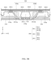
- FIG. 3A is a view of an electronic device in a first state (e.g. an unfolded state) with omission of a display to arrange an FPCB according to one embodiment
- FIG. 3B is a cross-sectional view of an FPCB of an electronic device in a first state according to one embodiment
- FIG. 3C is a cross-sectional view of an FPCB of an electronic device in a second state (e.g. a folded state) according to one embodiment.
- an electronic device 301 (e.g., the electronic device 101 of FIG. 1 and the electronic device 201 of FIG. 2A ) in one embodiment may include a display 350, a first housing 310, a second housing 320, a hinge structure 340, and an FPCB 390.
- the display 350 may include a first area 350a and a second area 350b, where the display 350 may fold (or bend) based on a folding axis. That is, the display 350 may be folded, or bent, along the folding axis, such that the first area 350a and the second area 350b form an area of the display 350 on either side of the folding axis.
- the first state e.g. an unfolded state
- the first area 350a and the second area 350b of the display 350 may form substantially the same plane.
- the second state e.g. a folded state
- the first area 350a and the second area 350b of the display 350 may face each other.
- first housing 310 and the second housing 320 may be rotatably connected to the hinge structure 340 on the folding axis.
- first housing 310 may form a first space 310a on the rear surface of the first area 350a and the second housing 320 may form a second space 320a on the rear surface of the second area 350b.
- the hinge structure 340 may rotatably connect the first housing 310 to the second housing 320.
- the hinge structure 340 may include a hinge housing 334, a first support plate 331, and a second support plate 332.
- a hinge space 334a may be formed in the hinge housing 334.
- first support plate 331 and the second support plate 332 may be rotatably connected to the hinge housing 334 based on the folding axis.
- first support plate 331 may connect the first housing 310 to the hinge housing 334
- second support plate 332 may connect the second housing 320 to the hinge housing 334.
- at least a portion of the first support plate 331 may be arranged in the first space 310a and the at least a portion of the second support plate 332 may be arranged in the second space 320a.
- At least one first opening 331a penetrating the surface of the first support plate 331 may be formed in the first support plate 331 and at least one second opening 332a penetrating the surface of the second support plate 332 may be formed in the second support plate 332.
- the FPCB 390 may electrically connect components arranged in the first space 310a and the second space 320a, for example, a first PCB (e.g., the first PCB 271 of FIG. 2C ) to a second PCB (e.g., the second PCB 272 of FIG. 2C ).
- the FPCB 390 may extend from the first space 310a to the second space 320a in an extending direction (e.g., the X-axis direction, in the direction of the longitudinal length of the FPCB, along its extending length, that is the direction in which the FPCB extends in a directional perpendicular to the folding axis) while traversing (e.g.
- the FPCB 390 may be arranged in the hinge space 334a formed by the hinge housing 334. Both ends of the FPCB 390 may extend to the first space 310a and the second space 320a through the first opening 331a and the second opening 332a, respectively.
- the FPCB 390 may be divided into a plurality of areas.
- the FPCB 390 may include a driving area (e.g., a driving area 391 of FIG. 4A ), a first fixed area (e.g., a first fixed area 392A of FIG. 4A ), and a second fixed area (e.g., a second fixed area 392B of FIG. 4A ).
- a driving area 391 of the FPCB 390 may be arranged in the hinge housing 334 and both ends of the driving area 391 may extend to the first support plate 331 and the second support plate 332, respectively.
- a driving area 391 of the FPCB 390 refers to the area that may be repeatedly driven (e.g. experiences an external driving, or bending, force) at an angle when the foldable device is open (or unfolded) state and closed (or folded) state.
- the driving area 391 may also be referred to as a bending area, a flexible area, or a deformable area. That is, in one embodiment, at least a portion of the driving area 391 may bend in response to a change (e.g.
- the driving area 391 may include a central portion 3911, a first bending portion 3912a, and a second bending portion 3912b, wherein the first bending portion 3912a and the second bending portion 3912b are respectively connected to both ends of the central portion 3911.
- the central portion 3911 may be arranged in the hinge space 334a.
- the first bending portion 3912a may extend from the central portion 3911 to the first support plate 331.
- the second bending portion 3912b may extend from the central portion 3911 to the second support plate 332.
- the first bending portion 3912a may extend from the hinge space 334a to the surface of the first support plate 331, and the second bending portion 3912b may extend from the hinge space 334a to the surface of the second support plate 332.
- the first bending portion 3912a and the second bending portion 3912b may partially bend in response to a change in a folding angle of the electronic device 301.
- the first and second bending portions 3912a and 3912b may bend and the shape of the driving area 391 of the FPCB 390 may change.
- the first fixed area 392A may extend from the driving area 391 to the first space 310a and the second fixed area 392B may extend from the driving area 391 to the second space 320a. In one embodiment, at least a portion of the first fixed area 392A may be fixed to the first housing 310 and at least a portion of the second fixed area 392B may be fixed to the second housing 320.
- the first fixed area 392A may include a first extension portion 3921 extending from the first bending portion 3912a in a direction (e.g., the -X direction of FIG. 3B ) opposite to the central portion 3911.
- the second fixed area 392B may include a second extension portion 3922 extending from the second bending portion 3912b in a direction (e.g., the +X direction of FIG. 3B ) opposite to the central portion 3911.
- first extension portion 3921 may be fixed to the first housing 310.
- an end, connected to the first bending portion 3912a, of the first extension portion 3921 may be fixed to the first support plate 331.
- the first extension portion 3921 may pass through the first opening 331a and may extend from the surface of the first support plate 331 to the inside the first space 310a.
- An end of the first extension portion 3921 extending to the inside the first space 310a may be fixed in the first space 310a.
- the end of the first extension portion 3921 extending to the inside the first space 310a may be connected to a component arranged in the first space 310a, for example, a first PCB (e.g., the first PCB 271 of FIG. 2C ).
- a first PCB e.g., the first PCB 271 of FIG. 2C
- at least a portion of the second extension portion 3922 may be fixed to the second housing 320.
- an end, connected to the second bending portion 3912b, of the second extension portion 3922 may be fixed to the second support plate 332.
- the second extension portion 3922 may pass through the second opening 332a and may extend from the surface of the second support plate 332 to the inside of the second space 320a.
- An end of the second extension portion 3922 extending to the inside of the second space 320a may be fixed in the second space 320a.
- the end of the second extension portion 3922 extending to the inside of the second space 320a may be connected to a component arranged in the second space 320a, for example, a second PCB (e.g., the second PCB 272 of FIG. 2C ).
- the FPCB 390 may be fixed to the first support plate 331 and the second support plate 332.
- the FPCB 390 may include a first fastening member 3931 fixed to the first support plate 331 and a second fastening member 3932 fixed to the second support plate 332.
- the first fastening member 3931 may fix a portion of the FPCB 390 to the surface of the first support plate 331 facing the display 350 and the second fastening member 3932 may fix a portion of the FPCB 390 to the surface of the second support plate 332 facing the display 350.
- a fastening member 393 may be coupled to the surface of the first or second support plate 331 or 332 through a coupling member (e.g., a screw and a fastener).
- a coupling member e.g., a screw and a fastener.
- the first fastening member 3931 may overlap the driving area 391 and the first fixed area 392A. That is, in an example, when the display 350 is viewed from above (e.g. when viewed downward, or -Z direction), the first fastening member 3931 may be seen to overlap the driving area 391 and the first fixed area 392A.
- the first fastening member 3931 may overlap the first bending portion 3912a and the first extension portion 3921.
- the second fastening member 3932 may overlap the driving area 391 and the second fixed area 392B. That is, in an example, when the display 350 is viewed from above (e.g. when viewed downward, or -Z direction), the second fastening member 3932 may be seen to overlap the driving area 391 and the second fixed area 392B For example, the second fastening member 3932 may overlap the second bending portion 3912b and the second extension portion 3922.
- the whole shape of the FPCB 390 may change in response to the shape of the electronic device 301.
- the electronic device 301 changes from the first state (e.g., the unfolded state of FIG. 3B ) to the second state (e.g., the folded state of FIG.
- the position (e.g., a position in the Z-axis direction) of the driving area 391 relative to the hinge housing 334 may change while simultaneously the first bending portion 3912a and the second bending portion 3912b are bent and the shape of the driving area 391 changes in response to the change in the folding angle of the electronic device 301.
- the first fixed area 392A and the second fixed area 392B of the FPCB 392 may maintain constant shapes (e.g. may maintain, or substantially maintain a current shape) in the electronic device 301 as the first fixed area 392A and the second fixed area 392B are partially fixed to the first housing 310 and the second housing 320, respectively.
- the first fixed area 392A and the second fixed area 392B may maintain relatively constant shapes compared to the driving area 391.
- relatively greater stress may be concentrated on the driving area 391 than the fixed area. That is, as the fixed areas (392A and 392B) of the FPCB 390 may be at least partially fixed to the respective housing, the shape (or position) of these areas of the FPCB 390 remains substantially constant (e.g. experiences a very small amount of bend when a folding angle of the electronic device 301 is changed), and these areas experience reduced stress in comparison to the driving area 391 (e.g. first and second bending portions 3912a and 3912b) which may be deformed, or bent, in shape in response to the change of folding angle.
- the driving area 391 e.g. first and second bending portions 3912a and 3912b
- FIG. 4A is a perspective view of an FPCB according to one embodiment
- FIG. 4B is a cross-sectional view of an FPCB taken along the line A-A of FIG. 4A .
- the FPCB 390 in one embodiment may include the driving area 391, the first fixed area 392A, and the second fixed area 392B divided in an extending direction (e.g., the X-axis direction, along a longitudinal length of the FPCB, that is, along a direction in which the FPCB extends).
- the first fixed area 392A and the second fixed area 392B may be connected to the driving area 391 opposite to each other (e.g. may form a fixed area of the FPCB 390 either side of the driving area 391). For example, based on FIG.
- the first fixed area 392A may be connected to the left side (e.g., the -X-axis direction) of the driving area 391 and the second fixed area 392B may be connected to the right side (e.g., the +X-axis direction) of the driving area 391.
- the first fastening member 3931 may be arranged on a connecting part of the driving area 391 to the first fixed area 392A and the second fastening member 3932 may be arranged on a connecting part of the driving area 391 to the second fixed area 392B.
- the driving area 391 may include the central portion 3911 arranged in a hinge housing (e.g., the hinge housing 334 of FIG. 3B ), the first bending portion 3912a extending from the central portion 3911 to the first fastening member 3931 and at least partially bending, and the second bending portion 3912b extending from the central portion 3911 to the second fastening member 3932 and at least partially bending.
- a hinge housing e.g., the hinge housing 334 of FIG. 3B
- the first bending portion 3912a extending from the central portion 3911 to the first fastening member 3931 and at least partially bending
- the second bending portion 3912b extending from the central portion 3911 to the second fastening member 3932 and at least partially bending.
- the first fixed area 392A may include the first extension portion 3921 extending from the first fastening member 3931 in a direction opposite to the central portion 3911.
- the second fixed area 392B may include the second extension portion 3922 extending from the second fastening member 3932 in a direction opposite to the central portion 3911.
- at least a portion of the first extension portion 3921 may be fixed to a first housing (e.g., the first housing 310 of FIG. 3B ) and at least a portion of the second extension portion 3922 may be fixed to a second housing (e.g., the second housing 320 of FIG. 3B ).
- a first connector 398a for connecting to a first component (e.g., the first PCB 271 of FIG.
- a second connector 398b for connecting to a second component (e.g., the second PCB 272 of FIG. 2C ) arranged in the second housing may be arranged on the second extension portion 3922.
- the FPCB 390 may comprise a multi-layer structure. That is, the FPCB 390 may be formed of a plurality of layers (or layer parts). In one embodiment, based on a cross-sectional view, the FPCB 390 may include (or be formed of) a first layer part 494, a second layer part 495, and a connecting layer 496 connecting the first layer part 494 to the second layer part 495. In one embodiment, as illustrated in FIG. 4B , the FPCB 390 may be arranged (or positioned) inside an electronic device such that the first layer part 494 faces the hinge housing and the second layer part 495 faces the rear surface of a display.
- the first layer part 494 may include (e.g. may be formed of) a first base layer 4944, a first metal layer 4943, a first adhesive layer 4942, and a first cover layer 4941.
- the first base layer 4944 may comprise (or be formed of) a PI material.
- the first base layer 4944 may include a first base surface and a second base surface opposite to the first base surface.
- the first base surface may face the rear surface (e.g., the +Z-axis direction) of the display and the second base surface may face the hinge housing (e.g., the -Z-axis direction).
- the first metal layer 4943 may be arranged on the first base surface of the first base layer 4944.
- the first metal layer 4943 may be formed of a conductive material, for example, copper (Cu).
- the first metal layer 4943 may form a plurality of signal lines (e.g., a signal line 5946 of FIG. 5B ) formed in an extending direction (e.g., along the X-axis) of the first base surface (e.g. of first base layer 4944).
- a pattern of the plurality of signal lines for transmitting a signal may be formed on the first metal layer 4943 through a process, such as etching.
- the plurality of signal lines may be formed to pass through the driving area 391 and extend from (and transmit signals from) the first fixed area 392A to the second fixed area 392B.
- a signal line formed in the first metal layer 4943 may be formed in a substantially straight line in an extending direction to perform high-speed signal transmission.
- the first cover layer 4941 may be stacked in a direction of the second base surface to cover the first metal layer 4943, for example, the plurality of signal lines. By covering the surface of the first metal layer 4943, the first cover layer 4941 may prevent damage to the plurality of signal lines formed on the first metal layer 4943.
- the first cover layer 4941 may be formed of a dielectric material.
- the first cover layer 4941 may be formed of PET.
- the first cover layer 4941 may have a different thickness depending on an area of the FPCB 390. A description thereof is provided later.
- the first adhesive layer 4942 may be arranged, or positioned, between the first metal layer 4943 and the first cover layer 4941. In one embodiment, the first adhesive layer 4942 may connect the first metal layer 4943 to the first cover layer 4941 to fill an empty space of the first metal layer 4943 of which the surface is etched to form a pattern of the signal line.
- the second layer part 495 may be stacked on the first layer part 494 in a direction of the first base surface of the first base layer 4944.
- the second layer part 495 may include a second base layer 4954, a second metal layer 4953, a second adhesive layer 4952, and a second cover layer 4951.
- the second base layer 4954 may be stacked on the first base layer 4944 to be opposite to the first metal layer 4943.
- the second base layer 4954 may be stacked in the direction of the first base surface of the first base layer 4944.
- the first base layer 4944 may include a PI material.
- the second metal layer 4953 may be arranged on the surface of the second base layer 4954 to be opposite to the first base layer 4944.
- the second metal layer 4953 may be formed a conductive material, for example, copper (Cu).
- the second metal layer 4953 may form a signal line extending from the first fixed area 392A to the second fixed area 392B.
- the second cover layer 4951 may be arranged on the second base layer 4954 to cover the second metal layer 4953.
- the second cover layer 4951 may be formed of a dielectric material, for example, PET.
- the second cover layer 4951 may be integrally formed to continue in the first fixed area 392A, the driving area 391, and the second fixed area 392B.
- the second adhesive layer 4952 may be between the second metal layer 4953 and the second cover layer 4951. In one embodiment, the second adhesive layer 4952 may connect the second metal layer 4953 to the second cover layer 4951 to fill an empty space of the second metal layer 4953 of which the surface is etched to form a pattern of the signal line.
- a connecting layer 496 may be disposed between the first layer part 494 and the second layer part 495.
- the connecting layer 496 may be formed of, for example, a polypropylene (PP) material.
- the thickness of the FPCB 390 when the FPCB 390 is formed having a double-layer structure including the first layer part 494 and the second layer part 495, in comparison to a larger number of layers of a FPCB structure, for example, the thickness of the FPCB 390 may therefore be decreased , and the thickness of an electronic device (e.g., the electronic device 301 of FIG. 3A ) may therefore also decrease. That is, the double-layer structure, according to the examples described, may reduce a thickness of the electronic device.
- FIG. 5A is a cross-sectional view of an FPCB according to one embodiment
- FIG. 5B is a view of an example of a plurality of signal lines according to one embodiment.
- an FPCB 590 in an embodiment may include a driving area 591, a first fixed area 592A, and a second fixed area 592B.
- the FPCB 590 may be formed such that the thickness of the driving area 591 is different from at least one of the thickness of the first fixed area 592A and the thickness of the second fixed area 592B.
- the thickness of the driving area 591 may be greater than the thickness of the first fixed area 592A and the thickness of the second fixed area 592B.
- the FPCB 590 may include a first layer part 594, a second layer part 595, and a connecting layer 596 connecting the first layer part 594 to the second layer part 595.
- the first layer part 594 include a first base layer 5944, a first metal layer 5943, a first adhesive layer 5942, and a first cover layer 5941.
- the second layer part 595 include a second base layer 5954, a second metal layer 5953, a second adhesive layer 5952, and a second cover layer 5951.
- the thickness of the driving area 591 of the first layer part 594 may be different from the thickness of the first layer part 594 in the first fixed area 592A and the thickness of the second fixed area 592B.
- the first cover layer 5941 may include a first cover portion 5941a arranged in the driving area 591 and having a first thickness t1, a second cover portion 5941b arranged in the first fixed area 592A and having a second thickness t2 that is different from the first thickness t1, and a third cover portion 5941c arranged in the second fixed area 592B and having a third thickness t3 that is different from the first thickness t1.
- the first cover portion 5941a, the second cover portion 5941b, and the third cover portion 5941c may be separately formed.
- first cover portion 5941a, the second cover portion 5941b, and the third cover portion 5941c may be individually formed and arranged on the first base layer 5944 to cover the first metal layer 5943.
- a first fastening member 5931 may be arranged on a boundary of a first cover portion 5941a and a second cover portion 5941b and a second fastening member 5932 may be arranged on a boundary of the first cover portion 5941a and a third cover portion 5941c.
- the first thickness t1 of the first cover portion 5941a may be greater than the second thickness t2 of the second cover portion 5941b and the third thickness t3 of the third cover portion 5941c.
- the first thickness t1 may be about twice the second thickness t2 or the third thickness t3.
- the second thickness t2 of the second cover portion 5941b may be substantially the same as the third thickness t3 of the third cover portion 5951c.
- the first thickness t1 may be greater than both the second thickness t2 and third thickness t3, wherein the second thickness t2 and third thickness t3 are substantially the same.
- the durability of the driving area 591 that changes its shape in response to a change in a folding angle may be improved compared to the fixed area, for example, the first fixed area 592A or the second fixed area 592B.
- the first or second fixed area 592A or 592B maintains a substantially constant shape regardless of a change in a folding angle, a space occupied by the FPCB 590 in the first housing (e.g., the first housing 310 of FIG. 3B ) and the second housing (e.g., the second housing 320 of FIG.
- the thickness e.g. a second thickness t2 and third thickness t3
- the driving area 591 e.g. a first thickness 11
- a plurality of signal lines 5946 formed by the first metal layer 5943 may form, on the first base layer 5944, a wiring pattern in a substantially straight line shape in an extending direction (e.g., the X-axis direction) for transmitting a high-speed signal.
- the plurality of signal lines 5946 may be arranged to extend in the extending direction and form intervals between each other (e.g. an interval, distance or spacing, between each of the plurality of signal lines 5946).
- the intervals between the plurality of signal lines 5946 may be different depending on an area of the FPCB 590.
- the plurality of signal lines 5946 may be arranged to form a first interval d1 between each other in the driving area 591. That is, a distance or spacing between signal lines (of the plurality of signal lines 5946 formed) in the driving area 591 may be at an interval (or spacing) of d1.
- the plurality of signal lines 5946 may be arranged to form a second interval d2 that is different from the first interval d1 between each other in the first fixed area 592A. That is, a distance or spacing between signal lines (of the plurality of signal lines 5946 formed) in the first fixed area 592A may be at an interval (or spacing) of d2.
- the plurality of signal lines 5946 may be arranged to form a third interval d3 that is different from the first interval d1 between each other in the second fixed area 592B.
- the second interval d2 between the plurality of signal lines 5946 in the first fixed area 592A may be less than the first interval d1 between the plurality of signal lines 5946 in the driving area 591.
- the third interval d3 between the plurality of signal lines 5946 in the second fixed area 592B may be less than the first interval d1 between the plurality of signal lines 5946 in the driving area 591.
- the second interval d2 may be substantially the same as the third interval d3.
- the second interval d2 and third interval d3 may be substantially the same, and less than the first interval d1.
- the first interval d1 between the plurality of signal lines 5946 in the driving area 591 may be about 1.2 times of the second interval d2 and the third interval d3 between the plurality of signal lines 5946 in the first fixed area 592A and the second fixed area 592B.
- the FPCB 590 may adjust an impedance difference among the driving area 591, the first fixed area 592A, and the second fixed area 592B to be within a set range through a thickness difference of areas of the first cover layer 5941 and an interval difference between the plurality of signal lines 5946 formed by the first metal layer 5943. That is, in other words, by the thickness differences of the first cover layer 5941 and/or the interval difference between the plurality of signal lines 5946 formed by the first metal layer 5943, the FPCB 590 may substantially match an impedance for the entire area. In one embodiment, an impedance value generated in each area of the FPCB 590 may increase as the thickness of the first cover layer 5941 formed of a dielectric material increases.
- the impedance value generated in each area of the FPCB 590 may increase as the interval between the plurality of signal lines 5946 formed by the first metal layer 5943 decreases.
- the FPCB 590 may provide an impedance match of the entire area by forming the first thickness t1 of the first cover portion 5951a in the driving area 591 to be greater than the second thickness t2 of the second cover portion 5951b in the first fixed area 592A and the third thickness t3 of the third cover portion 5951c in the second fixed area 592B and forming the first interval d1 between the plurality of signal lines 5946 in the driving area 591 to be greater than the second interval d2 between the plurality of signal lines 5946 in the first fixed area 592A and the third interval d3 between the plurality of signal lines 5946 in the second fixed area 592B.
- the first cover layer may have a thickness less in the driving area than a thickness in the first and second fixed areas.
- the first cover layer 5941 may have a thickness between 10 ⁇ m and 15 ⁇ m in the driving area 591. In one embodiment, the first cover layer 5941 may have a thickness between 12 ⁇ m and 13 ⁇ m in the driving area 591. In one embodiment, the first cover layer 5941 may have a thickness of about 12.5 ⁇ m in the driving area 591. In one embodiment, the first cover layer 5941 may have a thickness between 20 ⁇ m and 30 ⁇ m in the first fixed area 592A and the second fixed area 592B.
- the first cover layer 5941 may have a thickness between 24 ⁇ m and 26 ⁇ m in the first fixed area 592A and the second fixed area 592B. In one embodiment, the first cover layer 5941 may have a thickness of about 25 ⁇ m in the first fixed area 592A and the second fixed area 592B.
- An example where the first cover layer 5941 has a larger thickness in the first fixed area 592A and second fixed area 592B than the thickness of the driving area 591 is illustrated in Figure 6A-B .
- the plurality of signal lines 5946 formed by the first metal layer 5943 may be arranged to form an interval (e.g. interval d1) between each other between 45 ⁇ m and 55 ⁇ m in the driving area 591.
- the plurality of signal lines 5946 formed by the first metal layer 5943 may be arranged to form an interval between each other between 49 ⁇ m and 51 ⁇ m in the driving area 591. More preferably, the plurality of signal lines 5946 formed by the first metal layer 5943 may be arranged to form an interval between each other about 50 ⁇ m in the driving area 591.
- the plurality of signal lines 5946 formed by the first metal layer 5943 may be arranged to form an interval (e.g.
- the plurality of signal lines 5946 formed by the first metal layer 5943 may be arranged to form an interval between 59 ⁇ m and 61 ⁇ m between the first fixed area 592A and the second fixed area 592B. More preferably, the plurality of signal lines 5946 formed by the first metal layer 5943 may be arranged to form an interval of about 60 ⁇ m between the first fixed area 592A and the second fixed area 592B.
- An example where the plurality of signal lines are arranged to form a second and third interval in the respective first and second areas that is greater than the first interval formed between each other in the driving area is illustrated with reference to Figure 6A-B .
- Table 1 shown below may represent an example of adjusting the thickness of the first cover layer 5941 and an interval between the plurality of signal lines 5946 formed by the first metal layer 5943 to match impedances of each area of the FPCB 590. However, numerical values shown below are only an example for an impedance match and are not limited thereto.
- an impedance value of the FPCB 590 may increase as the thickness of the first cover layer 5941 formed of a dielectric material increases and may decrease as an interval between signal lines increases.
- the FPCB 590 may maintain impedance values of the driving area 591 and the fixed area to be within a set range by forming an interval between signal lines in the driving area 591 to be greater than an interval between signal lines in the fixed area while simultaneously improving the durability of the driving area 591 compared to the fixed area by increasing the thickness of the first cover layer 5941 in the driving area 591 compared to the fixed area.
- the first cover layer 5941 may have a thickness of about 25 ⁇ m in the driving area 591 and may have a thickness of about 12.5 ⁇ m in the fixed area.
- the plurality of signal lines formed on the first metal layer 5943 may have an interval of about 60 ⁇ m between each other in the driving area 591 and may have an interval of about 50 ⁇ m between each other in the fixed area.
- an impedance matching effect may be performed by means of adjustment (or difference) in the thickness of the first cover layer 5941 between driving area and fixed areas of the FPCB 590, and/or adjustment (or difference) in an interval between signal lines in the driving areas and the fixed areas of the FPCB, without being limited to the numerical values as described.
- FIG. 6A is a cross-sectional view of an FPCB according to one embodiment and FIG. 6B is a view of an example of a plurality of signal lines according to one embodiment.
- an FPCB 690 in an embodiment may include a driving area 691, a first fixed area 692A, and a second fixed area 692B.
- the thickness of the driving area 691 of the FPCB 690 may be less than at least one of the thickness of the first fixed area 692A and the thickness of the second fixed area 692B.
- the FPCB 690 may include a first base layer 6944, a first metal layer 6943, a first adhesive layer 6942, a first layer part 694 including a first cover layer 6941, a second base layer 6954, a second metal layer 6953, a second adhesive layer 6952, a second layer part 695 including a second cover layer 6951, and a connecting layer 696 connecting the first layer part 694 to the second layer part 695.
- the thickness of the driving area 691 of the first layer part 694 may be less than the thickness of the first fixed area 692A and the thickness of the second fixed area 692B.
- the first cover layer 6941 may include a first cover portion 6941a arranged in the driving area 691 and having a first thickness t1, a second cover portion 6941b arranged in the first fixed area 692A and having a second thickness t2 that is greater than the first thickness t1, and a third cover portion 6941c arranged in the second fixed area 692B and having a third thickness t3 that is greater than the first thickness t1.
- the first thickness t1 of the first cover portion 6941a may be less than the second thickness t2 of the second cover portion 6941b and the third thickness t3 of the third cover portion 6941c.
- the second thickness t2 and the third thickness t3 may be about twice the first thickness t1.
- durability of the first fixed area 692A and durability of the second fixed area 692B may be improved compared to the durability of the driving area 691.
- first fixed area 692A and the second fixed area 692B are respectively fixed to the first housing (e.g., the first housing 310 of FIG. 3B ) and the second housing (e.g., the second housing 320 of FIG. 3B )
- damage to the first fixed area 692A and the second fixed area 692B may be mitigated.
- first cover portion 6941a, the second cover portion 6941b, and the third cover portion 6941c may be separately formed.
- a first fastening member 6931 may be arranged on a boundary of the first cover portion 6941a and the second cover portion 6941b and a second fastening member 6932 may be arranged on a boundary of the first cover portion 6941a and the third cover portion 6941c.
- a plurality of signal lines 6946 formed by the first metal layer 6943 may form a wiring pattern in a substantially straight line shape in an extending direction (e.g., the X-axis direction) for transmitting a high-speed signal.
- the plurality of signal lines 6946 may be arranged to extend in the extending direction and form intervals between each other.
- an interval between the plurality of signal lines 6946 may be substantially the same or different by the area of the FPCB, e.g. in the driving area 691, the first fixed area 692A, and the second fixed area 692B.
- the plurality of signal lines 6946 may be arranged to form a first interval d1 between each other in the driving area 691.
- the plurality of signal lines 6946 may be arranged to form a second interval d2 that is substantially the same or different from the first interval d1 between each other in the first fixed area 692A.
- the plurality of signal lines 6946 may be arranged to form a third interval d3 that is substantially the same or greater than the first interval d1 between each other in the second fixed area 692B.
- the second interval d2 may be substantially the same as the third interval d3. In one embodiment, the second interval d2 and the third interval d3 between the plurality of signal lines 6946 in the fixed area may be about 1.2 times of the first interval d1 between the plurality of signal lines 6946 in the driving area.
- the first cover layer 6941 and the first adhesive layer 6942 of the FPCB 690 may be formed to have different thicknesses in each of the driving, first fixed, and second fixed areas 691, 692A, and 692B for impedance matching in each of the driving, first fixed, and second fixed areas 691, 692A, and 692B of the FPCB 690.
- the first cover layer 6941 and the first adhesive layer 6942 include a dielectric material
- the first cover layer 6941 and the first adhesive layer 6942 may have a complementary thickness difference depending on each of the driving, first fixed, and second fixed areas 691, 692A, and 692B of the FPCB 690, and thus, an impedance difference of the FPCB 690 may be in a set range.
- the thickness of the first adhesive layer 6942 in the driving area 691 may be less than the thickness of the first adhesive layer 6942 in the first or second fixed area 692A or 692B, and thus, an impedance difference for each of the driving, first fixed, and second fixed areas 691, 692A, and 692B based on a thickness difference of the first cover layer 6941 may be offset.
- an impedance difference of each of the driving, first fixed, and second fixed areas 691, 692A, and 692B of the FPCB 690 may decrease through a thickness difference of each of the driving, first fixed, and second fixed areas 691, 692A, and 692B of the first adhesive layer 6942 and the first cover layer 6941.
- the electronic device 101, 201, or 301 may include the display 250 or 350 including the first area 250a or 350a and the second area 250b or 350b, the first housing 210 or 310 supporting the first area 250a or 350a, the second housing 220 or 320 supporting the second area 250b or 350b, the hinge structure 340 foldably connecting the first housing 210 or 310 to the second housing 220 or 320 based on the folding axis A and adjusting a folding angle formed by the first housing 210 or 310 and the second housing 220 or 320 relative to the folding axis A, and the FPCB 290, 390, 590, or 690 extending in an extending direction.
- the FPCB 290, 390, 590, or 690 may include the driving area 391, 591, or 691 traversing the folding axis A and at least partially bending in response to a change in the folding angle, the first fixed area 392A, 592A, or 692A extending from the driving area 391, 591, or 691 to the first space 210a or 310a formed by the first housing 210 or 310, and the second fixed area 392B, 592B, or 692B extending from the driving area 391, 591, or 691 to the second space 220a or 320a formed by the second housing 220 or 320.
- the FPCB 290, 390, 590, or 690 may include the first base layer 4944, 5944, or 6944 including the first base surface and the second base surface opposite to the first base surface, the first metal layer 4943, 5943, or 6943 arranged on the second base surface and forming a plurality of signal lines 4946 extending in the extending direction, and the first cover layer 4941, 5941, or 6941 arranged to cover the first metal layer 4943, 5943, or 6943 in a direction of the second base surface.
- the thickness t1 of the first cover layer 4941, 5941, or 6941 in the driving area 391, 591, or 691 is different from the thickness t2 or t3 of the first cover layer 4941 in the first fixed area 392A, 592A, or 692A or the second fixed area 392B, 592B, or 692B.
- the first cover layer 4941, 5941, or 6941 may include the first cover portion 4941a, 5941a, or 6941a arranged in the driving area 491, 591, or 691 and having the first thickness t1, the second cover portion 4941b, 5941b, or 6941b arranged in the first fixed area 492A, 592A, or 692A and having the second thickness t2 that is different from the first thickness t2, and the third cover portion 4941c, 5941c, or 6941c arranged in the second fixed area 492B, 592B, or 692B and having the third thickness t3 that is different from the first thickness t1.
- the first cover portion 4941a, 5941a, or 6941a, the second cover portion 4941b, 5941b, or 6941b, and the third cover portion 4941c, 5941c, or 6941c may be separately formed.
- each of the cover portions having different thicknesses may be separately manufactured and arranged on the first base layer.
- the plurality of signal lines 5946 or 6946 may be arranged to extend in the extending direction and such that intervals are formed between the signal lines.
- the interval d1 between the plurality of signal lines 5946 or 6946 in the driving area 491, 591, or 691 may be different from the interval d2 or d3 between the plurality of signal lines 5946 or 6946 in the first fixed area 492A, 592A, or 692A or in the second fixed area 492B, 592B, or 692B.
- an impedance difference may occur according to an interval difference between the signal lines in each area of the FPCB.
- the first thickness t1 may be greater than the second thickness t2 and the third thickness t3.
- an impedance difference may occur according to the thickness of the first cover layer formed of a dielectric material.
- the plurality of signal lines 5946 may be arranged to form the first interval d1 between each other in the driving area 591. In one embodiment, the plurality of signal lines 5946 may be arranged to form the second interval d2 that is less than the first interval d1 between each other in the first fixed area 592A. In one embodiment, the plurality of signal lines 5946 may be arranged to form the third interval d3 that is less than the first interval d1 between each other in the second fixed area 592B.
- the first cover layer 5941 may have a thickness of 10 ⁇ m to 15 ⁇ m in the driving area 591. In one embodiment, the first cover layer 5941 may have a thickness of 20 ⁇ m to 30 ⁇ m in the first fixed area 592A and the second fixed area 592B. In one embodiment, the plurality of signal lines 5946 may be arranged to form an interval of 45 ⁇ m to 55 ⁇ m between each other in the driving area 591. In one embodiment, the plurality of signal lines 5946 may be arranged to form an interval of 54 ⁇ m to 66 ⁇ m between each other in the first fixed area 592A and the second fixed area 592B.
- the first thickness t1 may be less than the second thickness t2 and the third thickness t3.
- the plurality of signal lines 6946 may be arranged to form the first interval d1 between each other in the driving area 691. In one embodiment, the plurality of signal lines 6946 may be arranged to form the second interval d2 that is greater than the first interval d1 between each other in the first fixed area 692A. In one embodiment, the plurality of signal lines 6946 may be arranged to form the third interval d3 that is less than the first interval d1 between each other in the second fixed area 692B.
- the first cover layer 6941 may have a thickness of 20 ⁇ m to 30 ⁇ m in the driving area 601. In one embodiment, the first cover layer 6941 may have a thickness of 10 ⁇ m to 15 ⁇ m in the first fixed area 692A and the second fixed area 692B. In one embodiment, the plurality of signal lines 6946 may be arranged to form an interval of 55 ⁇ m to 65 ⁇ m between each other.
- the hinge structure 340 may further include the first support plate 331 connecting the first housing 310 to the hinge housing 346, and the second support plate 332 connecting the second housing 320 to the hinge housing 346.
- the FPCB 290, 390, 590, or 690 may further include the first fastening member 3931, 5931, or 6931 fixed to the first support plate 331, and the second fastening member 3932, 5932, or 6932 fixed to the second support plate 332.
- the first fastening member 3931, 5931, or 6931 may overlap the driving area 391, 591, or 691 and the first fixed area 392A, 592A, or 692A.
- the second fastening member 3932, 5932, or 6932 may overlap the driving area 391, 591, or 691 and the second fixed area 392B, 592B, or 692B.
- the driving area 391, 591, or 691 may include the central portion 3911, 5911, or 6911 arranged in the hinge housing 334, the first bending portion 3912a, 5912a, or 6912a extending from the central portion 3911, 5911, or 6911 to the first fastening member 3931, 5931, or 6931 and at least partially bending, and the second bending portion 3912b, 5912b, or 6912b extending from the central portion 3911, 5911, or 6911 to the second fastening member 3932, 5932, or 6932 and at least partially bending.
- the first fixed area 392A, 592A, or 692A may include the first extension portion 3921, 5921, or 6921 extending from the first fastening member 3931, 5931, or 6931 in a direction opposite to the central portion 3911, 5911, or 6911 and at least partially fixed to the first housing 210 or 310.
- the second fixed area 392B, 592B, or 692B may include the second extension portion 3922, 5922, or 6922 extending from the second fastening member 3932, 5932, or 6932 in a direction opposite to the central portion 3911, 5911, or 6911 and at least partially fixed to the second housing 220 or 320.
- the FPCB 390, 590, or 690 may further include the second base layer 4954, 5954, or 6954 arranged on the first base layer 4944, 5944, or 6944 to be opposite to the first metal layer 4943, 5943, or 6943, the second metal layer 4953, 5953, or 6953 arranged on the second base layer 4954, 5954, or 6954 to be opposite to the first base layer 4944, 5944, or 6944, and the second cover layer 4951, 5951, or 6951 arranged on the second base layer 4954, 5954, or 6954 to cover the second metal layer 4953, 5953, or 6953.
- the FPCB 390, 590, or 690 may be arranged such that the first base surface faces a rear surface of the display 250 or 350.
- the FPCB 290, 390, 590, or 690 arranged in the electronic device 201 or 301, the FPCB 290, 390, 590, or 690 may include the first base layer 4944, 5944, or 6944 including the first base surface and the second base surface opposite to the first base surface, the first metal layer 4943, 5943, or 6943 arranged on the second base surface and forming the plurality of signal lines 5946 or 6946 arranged in the extending direction, the first cover layer 4941, 5941, or 6941 arranged to cover the first metal layer 4943, 5943, or 6943 in a direction of the second base surface, the second base layer 4954, 5954, or 6954 arranged in a direction of the first base surface, the second metal layer 4953, 5953, or 6953 arranged on the second base layer 4954, 5954, or 6954 to be opposite to the first base layer 4944, 5944, or 6944, and the first base layer 49
- the FPCB 290, 390, 590, or 690 may include, based on the extending direction, the driving area 391, 591, or 691, the first fixed area 392A, 592A, or 692A, and the second fixed area 392B, 592B, or 692B, wherein the first fixed area 392A, 592A, or 692A and the second fixed area 392B, 592B, or 692B are arranged in opposite directions to each other relative to the driving area 391, 591, or 691.
- the thickness t1 of the first cover layer 4941, 5941, or 6941 in the driving area 391, 591, or 691 may be different from the thickness t2 or t3 of the first cover layer 4941, 5941, or 6941 in the first fixed area 392A, 592A, or 692A or the second fixed area 392B, 592B, or 692B.
- the first cover layer 5941 may include the first cover portion 5941a arranged in the driving area 591 and having the first thickness t1, the second cover portion 5941b arranged in the first fixed area 592A and having the second thickness t2 that is less than the first thickness t1, and the third cover portion 5941c arranged in the second fixed area 592B and having the third thickness t3 that is less than the first thickness t1.
- the plurality of signal lines 5946 or 6946 may extend in the extending direction and such that intervals are formed between the signal lines 5946 or 6946.
- the interval d1 between the plurality of signal lines 5946 or 6946 in the driving area 591 or 691 may be different from the interval d3 between the plurality of signal lines 5946 or 6946 in the first fixed area 592A or 691A or in the second fixed area 592B or 692B.
- the plurality of signal lines 5946 may be arranged to form the first interval d1 between each other in the driving area 591. In one embodiment, the plurality of signal lines 5946 may be arranged to form the second interval d2 that is less than the first interval d1 between each other in the first fixed area 592A. In one embodiment, the plurality of signal lines 5946 may be arranged to form the third interval d3 that is less than the first interval d1 between each other in the second fixed area 592B.
- the electronic device 201 or 301 may include the display 250 or 350 including the first area 250a or 350a and the second area 250b or 350b, the first housing 210 or 310 forming the first space 210a or 310a on a rear surface of the first area 250a or 350a, the second housing 220 or 320 forming the second space 220a or 320a on a rear surface of the second area 250b or 350b, the hinge structure 340 including the hinge housing 334 connecting the first housing 210 or 310 to the second housing 220 or 320 based on the folding axis A and adjusting a folding angle formed by the first housing 210 or 310 and the second housing 220 or 320, and the FPCB 290, 390, or 590 traversing the folding axis A and extending from the first space 210a or 310a to the second space 220a or 320a in the extending direction.
- the FPCB 290, 390, or 590 may include the driving area 391 or 591 at least partially arranged in the hinge housing 334 and at least partially bending in response to a change in the folding angle, the first fixed area 392A or 592A extending from the driving area 391 or 591 to the first space 210a or 310a, the second fixed area 392B or 592B extending from the driving area 391 or 591 to the second space 220a or 320a.
- the FPCB 290, 390, or 590 may include the first base layer 4944 or 5944 including the first base surface and the second base surface opposite to the first base surface, the first metal layer 4943 or 5943 arranged on the second base surface and forming the plurality of signal lines 5946 arranged in the extending direction, the first cover layer 4941 or 5941 arranged to cover the first metal layer 4943 or 5943 in a direction of the second base surface, the second base layer 4954 or 5954 arranged in a direction of the first base surface, the second metal layer 4953 or 5953 arranged on the second base layer 4954 or 5954 to be opposite to the first base layer 4944 or 5944, and the second cover layer 4951 or 5951 arranged on the second base layer 4954 or 5954 to cover the second metal layer 4953 or 5953.
- the thickness t1 of the first cover layer 4911 or 5911 in the driving area 391 or 591 may be greater than the thickness t2 of the first cover layer 4911 or 5911 in the first fixed area 392A or 592A or the second fixed area 392B or 592B.
- the interval d1 between the plurality of signal lines 5946 in the driving area 391 or 591 may be greater than the interval d2 or d3 between the plurality of signal lines 5946 in the first fixed area 392A or 592A or in the second fixed area 392B or 592B.
- the term driving area of the FPCB refers to the area that may be repeatedly driven (e.g. experiences an external driving, or bending, force) at an angle when the foldable device is open (or unfolded state) and closed (or folded state).
- the driving area may also be referred to as a bending area, a flexible area, or a deformable area.
- an extending direction may refer to an X-axis direction of the FPCB, a direction of the longitudinal length of the FPCB, that is the direction in which the FPCB extends in a direction perpendicular to the folding axis.
Landscapes
- Engineering & Computer Science (AREA)
- Computer Hardware Design (AREA)
- Physics & Mathematics (AREA)
- Theoretical Computer Science (AREA)
- Microelectronics & Electronic Packaging (AREA)
- Signal Processing (AREA)
- Mathematical Physics (AREA)
- Human Computer Interaction (AREA)
- General Engineering & Computer Science (AREA)
- General Physics & Mathematics (AREA)
- Telephone Set Structure (AREA)
Abstract
An electronic device including a flexible printed circuit board (FPCB) is provided. The electronic device includes a display including a first area and a second area, a first housing supporting the first area, a second housing supporting the second area, a hinge structure foldably connecting the first housing to the second housing based on a folding axis and adjusting a folding angle formed by the first housing and the second housing relative to the folding axis, and an FPCB extending in an extending direction.
Description
- The disclosure relates to a flexible printed circuit board., FPCB, and an electronic device comprising a flexible printed circuit board, FPCB.
- In recent years, electronic devices have progressed from devices having uniform rectangular shapes to devices having shapes of various designs and functions to satisfy purchasing desires of consumers. For example, such electronic devices may include foldable electronic devices that may be transformed in size according to use states (e.g. may be transformed from a folded state to an unfolded state). In such foldable electronic devices, a flexible printed circuit board (FPCB), which may flexibly change its shape, may be used to electrically connect various components within the device.
- According to one embodiment, an electronic device includes a display including a first area and a second area, a first housing supporting the first area, a second housing supporting the second area, a hinge structure foldably connecting the first housing to the second housing based on a folding axis and adjusting a folding angle formed by the first housing and the second housing relative to the folding axis, and a flexible printed circuit board (FPCB) extending in an extending direction. In one embodiment, the FPCB includes a driving area traversing the folding axis and at least partially bending in response to a change in the folding angle, a first fixed area extending from the driving area to a first space formed by the first housing, and a second fixed area extending from the driving area to a second space formed by the second housing. In one embodiment, the FPCB includes a first base layer including a first base surface and a second base surface opposite to the first base surface, a first metal layer arranged on the second base surface and forming a plurality of signal lines extending in the extending direction, and a first cover layer arranged to cover the first metal layer in a direction of the second base surface. In one embodiment, a thickness of the first cover layer in the driving area is different from a thickness of the first cover layer in the first fixed area or the second fixed area.
- According to one embodiment, an FPCB arranged in an electronic device includes a first base layer including a first base surface and a second base surface opposite to the first base surface, a first metal layer arranged on the second base surface and forming a plurality of signal lines arranged in an extending direction, a first cover layer arranged to cover the first metal layer in a direction of the second base surface, a second base layer arranged in a direction of the first base surface, a second metal layer arranged on the second base layer to be opposite to the first base layer, and a second cover layer arranged on the second base layer to cover the second metal layer. In one embodiment, the FPCB includes, based on the extending direction, a driving area, a first fixed area, and a second fixed area, wherein the first fixed area and the second fixed area are arranged in opposite directions to each other relative to the driving area. In one embodiment, a thickness of the first cover layer in the driving area is different from a thickness of the first cover layer in the first fixed area or the second fixed area.
- According to one embodiment, an electronic device includes a display including a first area and a second area, a first housing forming a first space on a rear surface of the first area, a second housing forming a second space on a rear surface of the second area, a hinge structure including a hinge housing connecting the first housing to the second housing based on the folding axis and adjusting a folding angle formed by the first housing and the second housing, and an FPCB traversing the folding axis and extending from the first space to the second space in the extending direction. In one embodiment, the FPCB includes a driving area at least partially arranged in the hinge housing and at least partially bending in response to a change in the folding angle, a first fixed area extending from the driving area to the first space, a second fixed area extending from the driving area to the second space. In one embodiment, the FPCB includes a first base layer including a first base surface and a second base surface opposite to the first base surface, a first metal layer arranged on the second base surface and forming a plurality of signal lines arranged in an extending direction, a first cover layer arranged to cover the first metal layer in a direction of the second base surface, a second base layer arranged in a direction of the first base surface, a second metal layer arranged on the second base layer to be opposite to the first base layer, and a second cover layer arranged on the second base layer to cover the second metal layer. In one embodiment, a thickness of the first cover layer in the driving area is greater than a thickness of the first cover layer in the first fixed area or the second fixed area. In one embodiment, an interval between the plurality of signal lines in the driving area is greater than an interval between the plurality of signal lines in the first fixed area or an interval between the plurality of signal lines in the second fixed area.
- The above and other aspects, features, and advantages of certain embodiments of the present disclosure will be more apparent from the following detailed description, taken in conjunction with the accompanying drawings, in which:
-
FIG. 1 is a block diagram of an electronic device in a network environment according to one embodiment; -
FIG. 2A is a view of an electronic device in a first state according to one embodiment; -
FIG. 2B is a view of an electronic device in a second state according to one embodiment; -
FIG. 2C is an exploded perspective view of an electronic device according to one embodiment; -
FIG. 3A is a view of an electronic device in a first state with omission of a display to arrange a flexible printed circuit board (FPCB) according to one embodiment; -
FIG. 3B is a cross-sectional view of an FPCB of an electronic device in a first state according to one embodiment; -
FIG. 3C is a cross-sectional view of an FPCB of an electronic device in a second state according to one embodiment; -
FIG. 4A is a perspective view of an FPCB according to one embodiment; -
FIG. 4B is a cross-sectional view of an FPCB taken along the line A-A ofFIG. 4A . -
FIG. 5A is a cross-sectional view of an FPCB according to one embodiment; -
FIG. 5B is a view of an example of a plurality of signal lines according to one embodiment; -
FIG. 6A is a cross-sectional view of an FPCB according to one embodiment; and -
FIG. 6B is a view of an example of a plurality of signal lines according to one embodiment. - Hereinafter, embodiments will be described in detail with reference to the accompanying drawings. When describing the embodiments with reference to the accompanying drawings, like reference numerals refer to like elements and a repeated description related thereto will be omitted.
-
FIG. 1 is a block diagram illustrating an electronic device in a network environment according to one embodiment. Referring toFIG. 1 , theelectronic device 101 in thenetwork environment 100 may communicate with anelectronic device 102 via a first network 198 (e.g., a short-range wireless communication network), or communicate with at least one of anelectronic device 104 or aserver 108 via a second network 199 (e.g., a long-range wireless communication network). According to one embodiment, theelectronic device 101 may communicate with theelectronic device 104 via theserver 108. According to one embodiment, theelectronic device 101 may include aprocessor 120, amemory 130, aninput module 150, asound output module 155, adisplay module 160, anaudio module 170, asensor module 176, aninterface 177, a connectingterminal 178, ahaptic module 179, acamera module 180, apower management module 188, abattery 189, acommunication module 190, a subscriber identification module (SIM) 196, or anantenna module 197. In some embodiments, at least one (e.g., the connecting terminal 178) of the above components may be omitted from theelectronic device 101, or one or more other components may be added in theelectronic device 101. In some embodiments, some (e.g., thesensor module 176, thecamera module 180, or the antenna module 197) of the components may be integrated as a single component (e.g., the display module 160). - The
processor 120 may execute, for example, software (e.g., a program 140) to control at least one other component (e.g., a hardware or software component) of theelectronic device 101 connected to theprocessor 120, and may perform various data processing or computation. According to one embodiment, as at least a portion of data processing or computation, theprocessor 120 may store a command or data received from another component (e.g., thesensor module 176 or the communication module 190) in avolatile memory 132, process the command or the data stored in thevolatile memory 132, and store resulting data in anon-volatile memory 134. According to one embodiment, theprocessor 120 may include a main processor 121 (e.g., a central processing unit (CPU) or an application processor (AP)), or an auxiliary processor 123 (e.g., a graphics processing unit (GPU), a neural processing unit (NPU), an image signal processor (ISP), a sensor hub processor, or a communication processor (CP)) that is operable independently from, or in conjunction with themain processor 121. For example, when theelectronic device 101 includes themain processor 121 and theauxiliary processor 123, theauxiliary processor 123 may be adapted to consume less power than themain processor 121 or to be specific to a specified function. Theauxiliary processor 123 may be implemented separately from themain processor 121 or as a part of themain processor 121. - The
auxiliary processor 123 may control at least some of functions or states related to at least one (e.g., thedisplay module 160, thesensor module 176, or the communication module 190) of the components of theelectronic device 101, instead of themain processor 121 while themain processor 121 is in an inactive (e.g., sleep) state or along with themain processor 121 while themain processor 121 is in an active state (e.g., executing an application). According to one embodiment, the auxiliary processor 123 (e.g., an ISP or a CP) may be implemented as a portion of another component (e.g., thecamera module 180 or the communication module 190) that is functionally related to theauxiliary processor 123. According to one embodiment, the auxiliary processor 123 (e.g., an NPU) may include a hardware structure specified for artificial intelligence (AI) model processing. An AI model may be generated by machine learning. Such learning may be performed by, for example, theelectronic device 101 in which artificial intelligence is performed, or performed via a separate server (e.g., the server 108). Learning algorithms may include, but are not limited to, for example, supervised learning, unsupervised learning, semi-supervised learning, or reinforcement learning. The AI model may include a plurality of artificial neural network layers. An artificial neural network may include, for example, a deep neural network (DNN), a convolutional neural network (CNN), a recurrent neural network (RNN), a restricted Boltzmann machine (RBM), a deep belief network (DBN), a bidirectional recurrent deep neural network (BRDNN), a deep Q-network, or a combination of two or more thereof, but is not limited thereto. The AI model may additionally or alternatively include a software structure other than the hardware structure. - The
memory 130 may store various data used by at least one component (e.g., theprocessor 120 or the sensor module 176) of theelectronic device 101. The various pieces of data may include, for example, software (e.g., the program 140) and input data or output data for a command related thereto. Thememory 130 may include thevolatile memory 132 or thenon-volatile memory 134. - The
program 140 may be stored as software in thememory 130 and may include, for example, an operating system (OS) 142,middleware 144, or anapplication 146. - The
input module 150 may receive a command or data to be used by another component (e.g., the processor 120) of theelectronic device 101, from the outside (e.g., a user) of theelectronic device 101. Theinput module 150 may include, for example, a microphone, a mouse, a keyboard, a key (e.g., a button), or a digital pen (e.g., a stylus pen). - The
sound output module 155 may output a sound signal to the outside of theelectronic device 101. Thesound output module 155 may include, for example, a speaker or a receiver. The speaker may be used for general purposes, such as playing multimedia or playing record. The receiver may be used to receive an incoming call. According to one embodiment, the receiver may be implemented separately from the speaker or as a part of the speaker. - The
display module 160 may visually provide information to the outside (e.g., a user) of theelectronic device 101. Thedisplay module 160 may include, for example, a control circuit for controlling a display, a hologram device, or a projector and control circuitry to control a corresponding one of the display, the hologram device, and the projector. According to one embodiment, thedisplay device 160 may include a touch sensor adapted to sense a touch, or a pressure sensor adapted to measure an intensity of a force incurred by the touch. - The
audio module 170 may convert a sound into an electric signal or vice versa. According to one embodiment, theaudio module 170 may obtain the sound via theinput device 150 or output the sound via thesound output device 155 or an external electronic device (e.g., anelectronic device 102 such as a speaker or a headphone) directly or wirelessly connected to theelectronic device 101. - The
sensor module 176 may detect an operational state (e.g., power or temperature) of theelectronic device 101 or an environmental state (e.g., a state of a user) external to theelectronic device 101, and generate an electrical signal or data value corresponding to the detected state. According to one embodiment, thesensor module 176 may include, for example, a gesture sensor, a gyro sensor, an atmospheric pressure sensor, a magnetic sensor, an acceleration sensor, a grip sensor, a proximity sensor, a color sensor, an infrared (IR) sensor, a biometric sensor, a temperature sensor, a humidity sensor, or an illuminance sensor. - The
interface 177 may support one or more specified protocols to be used for theelectronic device 101 to be coupled with the external electronic device (e.g., the electronic device 102) directly (e.g., by wire) or wirelessly. According to one embodiment, theinterface 177 may include, for example, a high-definition multimedia interface (HDMI), a universal serial bus (USB) interface, a secure digital (SD) card interface, or an audio interface. - The connecting
terminal 178 may include a connector via which theelectronic device 101 may be physically connected to an external electronic device (e.g., the electronic device 102). According to one embodiment, the connectingterminal 178 may include, for example, an HDMI connector, a USB connector, an SD card connector, or an audio connector (e.g., a headphone connector). - The
haptic module 179 may convert an electrical signal into a mechanical stimulus (e.g., a vibration or a movement) or an electrical stimulus which may be recognized by a user via his or her tactile sensation or kinesthetic sensation. According to one embodiment, thehaptic module 179 may include, for example, a motor, a piezoelectric element, or an electric stimulator. - The
camera module 180 may capture a still image and moving images. According to one embodiment, thecamera module 180 may include one or more lenses, image sensors, ISPs, or flashes. - The
power management module 188 may manage power supplied to theelectronic device 101. According to one embodiment, thepower management module 188 may be implemented as, for example, at least a part of a power management integrated circuit (PMIC). - The
battery 189 may supply power to at least one component of theelectronic device 101. According to one embodiment, thebattery 189 may include, for example, a primary cell which is not rechargeable, a secondary cell which is rechargeable, or a fuel cell. - The
communication module 190 may support establishing a direct (e.g., wired) communication channel or a wireless communication channel between theelectronic device 101 and the external electronic device (e.g., theelectronic device 102, theelectronic device 104, or the server 108) and performing communication via the established communication channel. Thecommunication module 190 may include one or more communication processors that are operable independently of the processor 120 (e.g., an AP) and that support a direct (e.g., wired) communication or a wireless communication. According to an example embodiment, thecommunication module 190 may include a wireless communication module 192 (e.g., a cellular communication module, a short-range wireless communication module, or a global navigation satellite system (GNSS) communication module) or a wired communication module 194 (e.g., a local area network (LAN) communication module, or a power line communication (PLC) module). A corresponding one of these communication modules may communicate with the externalelectronic device 104 via the first network 198 (e.g., a short-range communication network, such as Bluetooth™, wireless-fidelity (Wi-Fi) direct, or infrared data association (IrDA)) or the second network 199 (e.g., a long-range communication network, such as a legacy cellular network, a 5G network, a next-generation communication network, the Internet, or a computer network (e.g., a LAN or a wide area network (WAN)). These various types of communication modules may be implemented as a single component (e.g., a single chip), or may be implemented as multi components (e.g., multi chips) separate from each other. The wireless communication module 192 may identify and authenticate theelectronic device 101 in a communication network, such as thefirst network 198 or thesecond network 199, using subscriber information (e.g., international mobile subscriber identity (IMSI)) stored in theSIM 196. - The wireless communication module 192 may support a 5G network after a 4G network, and next-generation communication technology, e.g., new radio (NR) access technology. The NR access technology may support enhanced mobile broadband (eMBB), massive machine type communications (mMTC), or ultra-reliable and low-latency communications (URLLC). The wireless communication module 192 may support a high-frequency band (e.g., a mmWave band) to achieve, e.g., a high data transmission rate. The wireless communication module 192 may support various technologies for securing performance on a high-frequency band, such as, e.g., beamforming, massive multiple-input and multiple-output (MIMO), full dimensional MIMO (FD-MIMO), an array antenna, analog beam-forming, or a large scale antenna. The wireless communication module 192 may support various requirements specified in the
electronic device 101, an external electronic device (e.g., the electronic device 104), or a network system (e.g., the second network 199). According to one embodiment, the wireless communication module 192 may support a peak data rate (e.g., 20 Gbps or more) for implementing eMBB, loss coverage (e.g., 164 dB or less) for implementing mMTC, or U-plane latency (e.g., 0.5 ms or less for each of downlink (DL) and uplink (UL), or a round trip of 1 ms or less) for implementing URLLC. - The
antenna module 197 may transmit or receive a signal or power to or from the outside (e.g., the external electronic device) of theelectronic device 101. According to one embodiment, theantenna module 197 may include an antenna including a radiating element including a conductive material or a conductive pattern formed in or on a substrate (e.g., a printed circuit board (PCB)). According to one embodiment, theantenna module 197 may include a plurality of antennas (e.g., array antennas). In such a case, at least one antenna appropriate for a communication scheme used in a communication network, such as thefirst network 198 or thesecond network 199, may be selected by, for example, thecommunication module 190 from the plurality of antennas. The signal or the power may be transmitted or received between thecommunication module 190 and the external electronic device via the at least one selected antenna. According to one embodiment, another component (e.g., a radio frequency integrated circuit (RFIC)) other than the radiating element may be additionally formed as a part of theantenna module 197. - According to one embodiment, the
antenna module 197 may form a mmWave antenna module. According to an example embodiment, the mmWave antenna module may include a PCB, an RFIC disposed on a first surface (e.g., a bottom surface) of the PCB or adjacent to the first surface and capable of supporting a designated a high-frequency band (e.g., the mmWave band), and a plurality of antennas (e.g., array antennas) disposed on a second surface (e.g., a top or a side surface) of the PCB, or adjacent to the second surface and capable of transmitting or receiving signals in the designated high-frequency band. - At least some of the above-described components may be coupled mutually and communicate signals (e.g., commands or data) therebetween via an inter-peripheral communication scheme (e.g., a bus, general purpose input and output (GPIO), serial peripheral interface (SPI), or mobile industry processor interface (MIPI)).
- According to an example embodiment, commands or data may be transmitted or received between the
electronic device 101 and the externalelectronic device 104 via theserver 108 coupled with thesecond network 199. Each of the externalelectronic devices electronic device 101. According to one embodiment, all or some of operations to be executed by theelectronic device 101 may be executed at one or more of the externalelectronic devices electronic device 101 needs to perform a function or a service automatically, or in response to a request from a user or another device, theelectronic device 101, instead of, or in addition to, executing the function or the service, may request one or more external electronic devices to perform at least part of the function or the service. The one or more external electronic devices receiving the request may perform the at least part of the function or the service requested, or an additional function or an additional service related to the request, and may transfer an outcome of the performing to theelectronic device 101. Theelectronic device 101 may provide the result, with or without further processing the result, as at least part of a response to the request. To that end, cloud computing, distributed computing, mobile edge computing (MEC), or client-server computing technology may be used, for example. Theelectronic device 101 may provide ultra low-latency services using, e.g., distributed computing or mobile edge computing. In one embodiment, the externalelectronic device 104 may include an Internet-of-things (IoT) device. Theserver 108 may be an intelligent server using machine learning and/or a neural network. According to an example embodiment, the externalelectronic device 104 or theserver 108 may be included in thesecond network 199. Theelectronic device 101 may be applied to intelligent services (e.g., smart home, smart city, smart car, or healthcare) based on 5G communication technology or IoT-related technology. - The electronic device according to embodiments may be one of various types of electronic devices. The electronic device may include, for example, a portable communication device (e.g., a smartphone), a computer device, a portable multimedia device, a portable medical device, a camera, a wearable device, or a home appliance device. According to an example embodiment of the disclosure, the electronic device is not limited to those described above.
- It should be appreciated that various example embodiments of the present disclosure and the terms used therein are not intended to limit the technological features set forth herein to particular example embodiments and include various changes, equivalents, or replacements for a corresponding example embodiment. In connection with the description of the drawings, like reference numerals may be used for similar or related components. It is to be understood that a singular form of a noun corresponding to an item may include one or more of the things, unless the relevant context clearly indicates otherwise. As used herein, "A or B", "at least one of A and B", "at least one of A or B", "A, B or C", "at least one of A, B and C", and "A, B, or C," each of which may include any one of the items listed together in the corresponding one of the phrases, or all possible combinations thereof. Terms such as "first", "second", or "first" or "second" may simply be used to distinguish the component from other components in question, and may refer to components in other aspects (e.g., importance or order) is not limited. It is to be understood that if an element (e.g., a first element) is referred to, with or without the term "operatively" or "communicatively," as "coupled with," "coupled to," "connected with," or "connected to" another element (e.g., a second element), it means that the element may be coupled with the other element directly (e.g., by wire), wirelessly, or via a third element.
- As used in connection with various embodiments of the disclosure, the term "module" may include a unit implemented in hardware, software, or firmware, and may interchangeably be used with other terms, for example, "logic", "logic block", "part", or "circuitry". A module may be a single integral component, or a minimum unit or part thereof, adapted to perform one or more functions. For example, according to one embodiment, the module may be implemented in a form of an application-specific integrated circuit (ASIC).
- Various embodiments as set forth herein may be implemented as software (e.g., the program 140) including one or more instructions that are stored in a storage medium (e.g., an
internal memory 136 or an external memory 138) that is readable by a machine (e.g., the electronic device 101). For example, a processor (e.g., the processor 120) of the machine (e.g., the electronic device 101) may invoke at least one of the one or more instructions stored in the storage medium and execute it. This allows the machine to be operated to perform at least one function according to the at least one instruction invoked. The one or more instructions may include code generated by a compiler or code executable by an interpreter. The machine-readable storage medium may be provided in the form of a non-transitory storage medium. Here, the term "non-transitory" simply means that the storage medium is a tangible device, and does not include a signal (e.g., an electromagnetic wave), but this term does not differentiate between where data is semi-permanently stored in the storage medium and where the data is temporarily stored in the storage medium. - According to one embodiment, a method according to one embodiment of the disclosure may be included and provided in a computer program product. The computer program product may be traded as a product between a seller and a buyer. The computer program product may be distributed in the form of a machine-readable storage medium (e.g., compact disc read-only memory (CD-ROM)), or be distributed (e.g., downloaded or uploaded) online via an application store (e.g., PlayStore™), or between two user devices (e.g., smartphones) directly. If distributed online, at least part of the computer program product may be temporarily generated or at least temporarily stored in the machine-readable storage medium, such as memory of the manufacturer's server, a server of the application store, or a relay server.
- According to embodiments, each component (e.g., a module or a program) of the above-described components may include a single entity or multiple entities, and some of the multiple entities may be separately disposed in different components. According to embodiments, one or more of the above-described components may be omitted, or one or more other components may be added. Alternatively or additionally, a plurality of components (e.g., modules or programs) may be integrated into a single component. In such a case, according to embodiments, the integrated component may still perform one or more functions of each of the plurality of components in the same or similar manner as they are performed by a corresponding one of the plurality of components before the integration. According to embodiments, operations performed by the module, the program, or another component may be carried out sequentially, in parallel, repeatedly, or heuristically, or one or more of the operations may be executed in a different order or omitted, or one or more other operations may be added.
- In
FIG. 2A and other following drawings, illustrated is a spatial coordinate system defined by an X-axis, a Y-axis, and a Z-axis that are orthogonal to each other. The X-axis may represent a width direction of an electronic device, the Y-axis may represent a length direction of the electronic device, and the Z-axis may represent a height (or thickness) direction of the electronic device. -
FIG. 2A is a view of an electronic device in a first state (e.g. an unfolded, or open, state) according to one embodiment,FIG. 2B is a view of an electronic device in a second state (e.g. a folded, or closed, state) according to one embodiment, andFIG. 2C is an exploded perspective view of an electronic device according to one embodiment. - Referring to
FIGS. 2A to 2C , in one embodiment, an electronic device 201 (e.g., theelectronic device 101 ofFIG. 1 ) may include a pair ofhousings display module 160 ofFIG. 1 ) arranged in a space formed by the pair ofhousings display 250 is visually visible from the outside), in which thedisplay 250 is arranged, of theelectronic device 201 may be defined as the front surface of theelectronic device 201 and a surface opposite to the front surface thereof may be defined as the rear surface of theelectronic device 201. A surface surrounding a space between the front surface and the rear surface may be defined as a side surface of theelectronic device 201. - In one embodiment, an electronic device (e.g., the
electronic device 101 ofFIG. 1 ) may include afirst housing 210, asecond housing 220, a firstrear cover 215, a secondrear cover 225, ahinge structure 230, adisplay 250,PCBs 270, and a flexible PCB (FPCB) 290. In one embodiment, theelectronic device 201 may not be limited to the shape and combination relationship illustrated inFIGS. 2A and2B , and may have a component combination relationship in a different structure. - In one embodiment, the
first housing 210 and thesecond housing 220 may be arranged on both sides of a folding axis A and may be substantially symmetrical to the folding axis A. In one embodiment, an angle or a distance mutually formed by thefirst housing 210 and thesecond housing 220 may vary depending on a state of theelectronic device 201. For example, depending on whether theelectronic device 201 is in a first state (e.g., an unfolded state) as illustrated inFIG. 2A , a second state (e.g., a folded state) as illustrated inFIG. 2B , or an intermediate state between the first state and the second state, a distance or an angle mutually formed by (or between) thefirst housing 210 and thesecond housing 220 may vary. - In one embodiment, the
first housing 210 may include a first surface facing the front surface of theelectronic device 201, a second surface opposite to the first surface, and a first side portion enclosing at least a portion of a space between the first surface and the second surface. Thesecond housing 220 may include a third surface facing the front surface of theelectronic device 201, a fourth surface opposite to the third surface, and a second side portion enclosing at least a portion of a space between the third surface and the fourth surface. The first surface and the third surface may face each other when theelectronic device 201 is in the folded state as illustrated inFIG. 2B . - In one embodiment, the
first housing 210 and thesecond housing 220 may form a recess of which a front surface is open to accommodate thedisplay 250. In one embodiment, at least a portion of thefirst housing 210 and thesecond housing 220 may be formed of a metal material or a non-metal material having appropriate rigidness to support thedisplay 250. In one embodiment, at least a portion of thefirst housing 210 and thesecond housing 220 formed of a metal material may provide a ground plane of theelectronic device 201 and may be electrically connected to a ground line formed on thePCB 270 arranged inside theelectronic device 201. - In one embodiment, the
electronic device 201 may include at least one component to perform various functions, wherein the component is exposed at the front surface of theelectronic device 201 through at least one opening formed in the front surface of the foldableelectronic device 201. For example, the component may include at least one of a front camera module, a receiver, a proximity sensor, an illuminance sensor, an iris recognition sensor, an ultrasonic sensor, or an indicator. - In one embodiment, the first
rear cover 215 and the secondrear cover 225 may be arranged on the rear surface of theelectronic device 201. For example, the firstrear cover 215 may be arranged on the second surface of thefirst housing 210 and the secondrear cover 225 may be arranged on the fourth surface of thesecond housing 220. At least a portion of an edge of the firstrear cover 215 may be enclosed by thefirst housing 210 and at least a portion of an edge of the secondrear cover 225 may be enclosed by thesecond housing 220. - In one embodiment, the first
rear cover 215 and the secondrear cover 225 may have substantially symmetrical shapes based on the folding axis A. In one embodiment, the firstrear cover 215 and the secondrear cover 225 may have different shapes. In one embodiment, thefirst housing 210 and the firstrear cover 215 may be integrally formed as one and thesecond housing 220 and the secondrear cover 225 may be integrally formed as one. - In an example embodiment, the
first housing 210, thesecond housing 220, the firstrear cover 215, and the secondrear cover 225 may provide a space in which various components (e.g., a PCB, theantenna module 197 ofFIG. 1 , thesensor module 176 ofFIG. 1 , or thebattery 189 ofFIG. 1 ) of theelectronic device 201 may be arranged through a structure in which thefirst housing 210, thesecond housing 220, the firstrear cover 215, and the secondrear cover 225 are coupled to one another. In an example embodiment, at least one component may be visually exposed on the rear surface of theelectronic device 201. For example, at least a portion of a sub-display may be visually exposed through a firstrear area 216 of the firstrear cover 215. In one embodiment, at least one component may be visually exposed through a secondrear area 226 of the secondrear cover 225. In this case, the component may include a proximity sensor, a rear camera module, and/or a flash. - In one embodiment, the
display 250 may be arranged in a space formed by afoldable housing 201. For example, thedisplay 250 may be arranged in a recess formed by the pair ofhousings display 250 may be arranged to constitute most of the front surface of theelectronic device 201. The front surface of theelectronic device 201 may include an area accommodating thedisplay 250, a partial area (e.g., an edge area) of thefirst housing 210 adjacent to thedisplay 250, and a partial area (e.g., an edge area) of thesecond housing 220. The rear surface of theelectronic device 201 may include the firstrear cover 215, a partial area (e.g., an edge area) of thefirst housing 210 adjacent to the firstrear cover 215, the secondrear cover 225, and a partial area (e.g., an edge area) of thesecond housing 220 adjacent to the secondrear cover 225. In one embodiment, at least a partial area of thedisplay 250 may be deformed into a planar or curved surface. - In one embodiment, at least a partial area of the
display 250 may be deformed. In one embodiment, thedisplay 250 may include afolding area 250c arranged along the folding axis A, afirst area 250a arranged on a first side (e.g., the left side of thefolding area 250c ofFIG. 2A ) based on thefolding area 250c, and asecond area 250b arranged on a second side (e.g., the right side of thefolding area 250c ofFIG. 2A ) based on thefolding area 250c. In one embodiment, thefirst area 250a may be supported by thefirst housing 210 and thesecond housing 250b may be supported by thesecond housing 220. However, the illustrated area division of thedisplay 250 is an example, and thedisplay 250 may be divided into a plurality of areas depending on the structure or functions of thedisplay 250. For example, as illustrated inFIG. 2A , thedisplay 250 may be divided into areas based on the folding area 203 extending in parallel to the folding axis A. In another example, thedisplay 250 may be divided into areas based on another folding axis (e.g., a folding axis parallel with a width direction of an electronic device). - According to one embodiment, the
display 250 may be coupled to or disposed adjacent to a touch panel in which a touch sensing circuit and a pressure sensor configured to measure an intensity (or pressure) of a touch are provided. For example, thedisplay 250 may be coupled to or disposed adjacent to a touch panel for detecting a stylus pen of an electromagnetic resonance (EMR) type, as an example of the touch panel. - According to one embodiment, the
first area 250a and thesecond area 250b may generally have symmetrical shapes with respect to thefolding area 250c. In one embodiment, a notch that is at least a partial cut to expose a sensor may be formed in at least one of thefirst area 250a and thesecond area 250b. For example, thefirst area 250a and thesecond area 250b may include portions having mutually symmetrical shapes and portions having mutually asymmetrical shapes. - In one embodiment, the
hinge structure 230 may be arranged between thefirst housing 210 and thesecond housing 220 and may include ahinge cover 265 to cover a space between thefirst housing 210 and thesecond housing 220. In one embodiment, thehinge cover 265 may be visually exposed to the outside or occluded by thefirst housing 210 and thesecond housing 220, based on an operational state of theelectronic device 201 For example, when theelectronic device 201 is in the first state as illustrated inFIG. 2A , thehinge cover 265 may be occluded by thefirst housing 210 and thesecond housing 220 and not be exposed to the outside, and when theelectronic device 201 is in the second state as illustrated inFIG. 2B , thehinge cover 265 may be visually exposed to the outside between thefirst housing 210 and thesecond housing 220. - When the
electronic device 201 is in the intermediate state forming an angle between the first state ofFIG. 2A and the second state ofFIG. 2B , at least a portion of thehinge cover 265 may be exposed to the outside between thefirst housing 210 and thesecond housing 220 and in this case, an area of thehinge cover 265 exposed to the outside may be less than an exposed area of thehinge cover 265 in the second state (e.g., a folded state) of theelectronic device 201. In one embodiment, thehinge cover 265 may include a curved shape. - In one embodiment, when the
electronic device 201 is in the first state (e.g., an unfolded state ofFIG. 2A ), thefirst housing 210 and thesecond housing 220 may form a first angle (e.g., about 180 degrees) with each other and thefirst area 250a and thesecond area 250b of thedisplay 250 may be oriented in substantially the same direction and may form substantially the same plane. In this case, thefolding area 250c of thedisplay 250 may be on substantially the same plane as thefirst area 250a and thesecond area 250b. In one embodiment, when theelectronic device 201 is in the unfolded state, as thefirst housing 210 rotates at a second angle (e.g., about 360 degrees) relative to thesecond housing 220, the second surface and the fourth surface may be reversely folded to face each other. - In one embodiment, when the
electronic device 201 is in the second state (e.g., the folded state ofFIG. 2B ), thefirst housing 210 and thesecond housing 220 may face each other. In this case, thefirst area 250a and thesecond area 250b of thedisplay 250 may form a narrow angle (e.g., 0 to 10 degrees) therebetween and may face each other. In this case, at least a portion of thefolding area 250c of thedisplay 250 may be deformed into a curved surface. - In one embodiment, when the
electronic device 201 is in an intermediate state between the first state and the second state (e.g., an intermediate open state), thefirst housing 210 and thesecond housing 220 may be arranged to form a predetermined angle. The surface of thefirst area 250a and the surface of thesecond area 250b of thedisplay 250 may form an angle greater than that in the second state (e.g., a folded state) and less than that in the first state (e.g., a fully open state). At least a portion of thefolding area 250c may include a curved surface and in this case, the curvature may be less than that in the second state (e.g., the folded state). - In one embodiment, the
display 250 may include a display panel 251 (e.g., a flexible display panel) and at least oneplate 252 or a layer arranged on the rear surface of thedisplay panel 251. - In one embodiment, the
display panel 251 may include a flexible display substrate, a plurality of display elements coupled to the display substrate to form pixels, one or more conductive lines coupled to the display substrate and electrically connected to other display elements, and a thin-film encapsulation layer configured to prevent inflow of external oxygen and moisture. Thedisplay panel 251 may include a touch panel, or thedisplay panel 251 and the touch panel may be integrally formed therewith. - The display substrate may be formed of a flexible material, for example, a plastic material, such as polyimide (PI), but the material of the display substrate is not limited thereto and may include other flexible materials. The plurality of display elements may be arranged on the display substrate and form some pixels. For example, the plurality of display elements may be arranged in a matrix form on the display substrate to form pixels of the
display panel 251. In this case, the plurality of display elements may include a fluorescent material or an organic fluorescent material that may express colors. For example, the display elements may include organic light-emitting diodes (OLEDs). The conductive lines may include one or more gate signal lines or one or more data signal lines. For example, the conductive lines may include a plurality of gate signal lines and a plurality of data signal lines, and the plurality of gate signal lines and the plurality of data signal lines may be arranged in a matrix form. In this case, the plurality of display elements may be arranged adjacent to a point where a plurality of lines intersect, and may be electrically connected to each line. The thin film encapsulation layer may cover the display substrate, the plurality of display elements, and the conductive lines, thereby preventing inflow of oxygen and moisture from an outside. In one embodiment, the thin film encapsulation layer may be formed by alternately stacking one or more organic film layers and one or more inorganic film layers. - In one embodiment, the touch panel may be formed as an integral body with the
display panel 251 or attached thereto. For example, the touch panel may be formed by patterning an aluminum metal mesh sensor on the thin film encapsulation layer of thedisplay panel 251. - In one embodiment, the polarizing film may be stacked between the
display panel 251 and the touch panel. The polarizing film may improve visibility of thedisplay 250. The polarizing film may change a phase of light passing through thedisplay 250. For example, the polarizing film may convert linearly polarized light into circularly polarized light or convert circularly polarized light into linearly polarized light, thereby preventing reflection of light incident to thedisplay panel 251. - The window layer may be formed of a transparent plastic film having high flexibility and high hardness. For example, the window layer may be formed of a PI or polyethylene terephthalate (PET) film. In one embodiment, the window layer may be formed as multiple layers including a plurality of plastic films.
- In one embodiment, the
plate 252 may support the rear surface of thedisplay panel 251, thereby improving the impact resistance of thedisplay panel 251. In one embodiment, theplate 252 may be divided into areas to support a rear surface of thefirst area 250a and a rear surface of thesecond area 250b of thedisplay panel 251, respectively. In this case, the respective areas of theplate 252 may be separately attached to the rear surface of thefirst area 250a and the rear surface of thesecond area 250b of thedisplay 250 so as not to contact each other along the folding axis A. According to this structure, theplate 252 may not interfere with the folding operation of thedisplay 250 performed along the folding axis A. - In one embodiment, the
plate 252 may be formed of a conductive material, for example, copper or an alloy material including copper. In this case, theplate 251 may function as a heat transfer path that transfers heat generated by an internal component (e.g., an AP) of theelectronic device 201 to thedisplay panel 251 while improving the impact resistance of thedisplay 250. - The
hinge structure 230 may include afirst support plate 231, asecond support plate 232, ahinge housing 234 between thefirst support plate 231 and thesecond support plate 232, and aFPCB 290 arranged to traverse thefirst support plate 231 and thesecond support plate 232. In one embodiment, theFPCB 290 may be a FPCB. - In one embodiment, the
first support plate 231 may be in a rear direction of thefirst area 250a of thedisplay 250 and thesecond support plate 232 may be in a rear direction of thesecond area 250b of thedisplay 250. In one embodiment, thefirst support plate 231 may be connected to a first side (e.g., the -X direction ofFIG. 2C ) of thehinge housing 234 and thesecond support plate 232 may be connected to a second side (e.g., the +X direction ofFIG. 2C ) of thehinge housing 234. Thefirst support plate 231 may be inserted into afirst space 210a inside thefirst housing 210 and thesecond support plate 232 may be inserted into asecond space 220a inside thesecond housing 220, and thus, thefirst housing 210 and thesecond housing 220 may be connected to thehinge structure 230. - In one embodiment, the
first housing 210 may include a firstrotation support surface 214, and thesecond housing 220 may include a secondrotation support surface 224 corresponding to the firstrotation support surface 214. The firstrotation support surface 214 and the secondrotation support surface 224 may include curved surfaces corresponding to the curved surfaces included in thehinge cover 265. - In one embodiment, when the
electronic device 201 is in an unfolded state (e.g., theelectronic device 201 ofFIG. 2A ), the firstrotation support surface 214 and the secondrotation support surface 224 may cover thehinge cover 265 such that thehinge cover 265 may not be exposed through the rear surface of theelectronic device 201 or may be minimally exposed. Meanwhile, when theelectronic device 201 is in a folded state (e.g., theelectronic device 201 ofFIG. 2B ), the firstrotation support surface 214 and the secondrotation support surface 224 may rotate along the curved surfaces included in thehinge cover 265 such that thehinge cover 265 may be maximally exposed through the rear surface of theelectronic device 201. - In one embodiment, the
PCB 270 may include afirst PCB 271 arranged on the side of thefirst support plate 231 and asecond PCB 272 arranged on the side of thesecond support plate 232. Thefirst PCB 271 and thesecond PCB 272 may be arranged inside a space formed by thehinge structure 230, thefirst housing 210, thesecond housing 220, the firstrear cover 215, and the secondrear cover 225. For example, thefirst PCB 271 may be arranged in thefirst space 210a inside thefirst housing 210 and thesecond PCB 272 may be arranged in thesecond space 220a inside thesecond housing 220. In this case, thefirst PCB 271 may be arranged between thefirst support plate 231 and the rear surface of thefirst housing 210 and thesecond PCB 272 may be arranged between thesecond support plate 232 and the rear surface of thesecond housing 220. Components for implementing various functions of theelectronic device 201 may be mounted on thefirst PCB 271 and thesecond PCB 272. - In one embodiment, the
FPCB 290 may connect components arranged inside thefirst housing 210 and thesecond housing 220. For example, theFPCB 290 may connect a first electronic or electrical component arranged inside the first housing 210 (e.g. within a first space), and a second electronic or electrical component arranged inside the second housing 220 (e.g. within a second space). In an example, , theFPCB 290 may connect the first FPCB 271 (e.g. arranged in afirst space 210a inside the first housing 210) to the second FPCB 272 (e.g. arranged in thesecond space 220a inside the second housing 220). In some examples, theFPCB 290 may be connected to thehinge structure 230. At least a portion of theFPCB 290 may be arranged in a space formed by thehinge housing 234 and both ends of theFPCB 290 may extend to thefirst space 210a and thesecond space 220b by penetrating thefirst support plate 231 and thesecond support plate 232, respectively. In one embodiment, theFPCB 290 may be arranged in a direction (e.g., the X-axis direction ofFIG. 2C ) perpendicular to the folding axis A of theelectronic device 201. -
FIG. 3A is a view of an electronic device in a first state (e.g. an unfolded state) with omission of a display to arrange an FPCB according to one embodiment,FIG. 3B is a cross-sectional view of an FPCB of an electronic device in a first state according to one embodiment, andFIG. 3C is a cross-sectional view of an FPCB of an electronic device in a second state (e.g. a folded state) according to one embodiment. - Referring to
FIGS. 3A to 3C , an electronic device 301 (e.g., theelectronic device 101 ofFIG. 1 and theelectronic device 201 ofFIG. 2A ) in one embodiment may include adisplay 350, afirst housing 310, asecond housing 320, ahinge structure 340, and anFPCB 390. - In one embodiment, the
display 350 may include afirst area 350a and asecond area 350b, where thedisplay 350 may fold (or bend) based on a folding axis. That is, thedisplay 350 may be folded, or bent, along the folding axis, such that thefirst area 350a and thesecond area 350b form an area of thedisplay 350 on either side of the folding axis. In the first state (e.g. an unfolded state) as illustrated inFIG. 3B , thefirst area 350a and thesecond area 350b of thedisplay 350 may form substantially the same plane. In the second state (e.g. a folded state) as illustrated inFIG. 3C , thefirst area 350a and thesecond area 350b of thedisplay 350 may face each other. - In one embodiment, the
first housing 310 and thesecond housing 320 may be rotatably connected to thehinge structure 340 on the folding axis. In one embodiment, thefirst housing 310 may form afirst space 310a on the rear surface of thefirst area 350a and thesecond housing 320 may form asecond space 320a on the rear surface of thesecond area 350b. - In one embodiment, the
hinge structure 340 may rotatably connect thefirst housing 310 to thesecond housing 320. In one embodiment, thehinge structure 340 may include ahinge housing 334, afirst support plate 331, and asecond support plate 332. In one embodiment, ahinge space 334a may be formed in thehinge housing 334. - In one embodiment, the
first support plate 331 and thesecond support plate 332 may be rotatably connected to thehinge housing 334 based on the folding axis. For example, thefirst support plate 331 may connect thefirst housing 310 to thehinge housing 334, and thesecond support plate 332 may connect thesecond housing 320 to thehinge housing 334. In one embodiment, at least a portion of thefirst support plate 331 may be arranged in thefirst space 310a and the at least a portion of thesecond support plate 332 may be arranged in thesecond space 320a. In one embodiment, at least onefirst opening 331a penetrating the surface of thefirst support plate 331 may be formed in thefirst support plate 331 and at least onesecond opening 332a penetrating the surface of thesecond support plate 332 may be formed in thesecond support plate 332. - In one embodiment, the
FPCB 390 may electrically connect components arranged in thefirst space 310a and thesecond space 320a, for example, a first PCB (e.g., thefirst PCB 271 ofFIG. 2C ) to a second PCB (e.g., thesecond PCB 272 ofFIG. 2C ). In one embodiment, theFPCB 390 may extend from thefirst space 310a to thesecond space 320a in an extending direction (e.g., the X-axis direction, in the direction of the longitudinal length of the FPCB, along its extending length, that is the direction in which the FPCB extends in a directional perpendicular to the folding axis) while traversing (e.g. extending across) the folding axis. In one embodiment, at least a portion of theFPCB 390 may be arranged in thehinge space 334a formed by thehinge housing 334. Both ends of theFPCB 390 may extend to thefirst space 310a and thesecond space 320a through thefirst opening 331a and thesecond opening 332a, respectively. - In one embodiment, based on the extending direction (e.g., the X-axis direction, a longitudinal length of the FPCB), the
FPCB 390 may be divided into a plurality of areas. For example, theFPCB 390 may include a driving area (e.g., a drivingarea 391 ofFIG. 4A ), a first fixed area (e.g., a first fixedarea 392A ofFIG. 4A ), and a second fixed area (e.g., a second fixedarea 392B ofFIG. 4A ). - In one embodiment, at least a portion of the driving
area 391 of theFPCB 390 may be arranged in thehinge housing 334 and both ends of the drivingarea 391 may extend to thefirst support plate 331 and thesecond support plate 332, respectively. In examples, a drivingarea 391 of theFPCB 390 refers to the area that may be repeatedly driven (e.g. experiences an external driving, or bending, force) at an angle when the foldable device is open (or unfolded) state and closed (or folded) state. In examples, the drivingarea 391 may also be referred to as a bending area, a flexible area, or a deformable area. That is, in one embodiment, at least a portion of the drivingarea 391 may bend in response to a change (e.g. a driven change, such as by a user) in a folding angle of theelectronic device 301. In one embodiment, the drivingarea 391 may include acentral portion 3911, afirst bending portion 3912a, and asecond bending portion 3912b, wherein thefirst bending portion 3912a and thesecond bending portion 3912b are respectively connected to both ends of thecentral portion 3911. - In one embodiment, the
central portion 3911 may be arranged in thehinge space 334a. In one embodiment, thefirst bending portion 3912a may extend from thecentral portion 3911 to thefirst support plate 331. Thesecond bending portion 3912b may extend from thecentral portion 3911 to thesecond support plate 332. For example, thefirst bending portion 3912a may extend from thehinge space 334a to the surface of thefirst support plate 331, and thesecond bending portion 3912b may extend from thehinge space 334a to the surface of thesecond support plate 332. In one embodiment, thefirst bending portion 3912a and thesecond bending portion 3912b may partially bend in response to a change in a folding angle of theelectronic device 301. For example, in response to a change in a folding state of theelectronic device 301, the first andsecond bending portions area 391 of theFPCB 390 may change. - In one embodiment, the first fixed
area 392A may extend from the drivingarea 391 to thefirst space 310a and the second fixedarea 392B may extend from the drivingarea 391 to thesecond space 320a. In one embodiment, at least a portion of the first fixedarea 392A may be fixed to thefirst housing 310 and at least a portion of the second fixedarea 392B may be fixed to thesecond housing 320. In one embodiment, the first fixedarea 392A may include afirst extension portion 3921 extending from thefirst bending portion 3912a in a direction (e.g., the -X direction ofFIG. 3B ) opposite to thecentral portion 3911. The second fixedarea 392B may include asecond extension portion 3922 extending from thesecond bending portion 3912b in a direction (e.g., the +X direction ofFIG. 3B ) opposite to thecentral portion 3911. - In one embodiment, at least a portion of the
first extension portion 3921 may be fixed to thefirst housing 310. For example, an end, connected to thefirst bending portion 3912a, of thefirst extension portion 3921 may be fixed to thefirst support plate 331. Thefirst extension portion 3921 may pass through thefirst opening 331a and may extend from the surface of thefirst support plate 331 to the inside thefirst space 310a. An end of thefirst extension portion 3921 extending to the inside thefirst space 310a may be fixed in thefirst space 310a. For example, the end of thefirst extension portion 3921 extending to the inside thefirst space 310a may be connected to a component arranged in thefirst space 310a, for example, a first PCB (e.g., thefirst PCB 271 ofFIG. 2C ). In one embodiment, at least a portion of thesecond extension portion 3922 may be fixed to thesecond housing 320. For example, an end, connected to thesecond bending portion 3912b, of thesecond extension portion 3922 may be fixed to thesecond support plate 332. Thesecond extension portion 3922 may pass through thesecond opening 332a and may extend from the surface of thesecond support plate 332 to the inside of thesecond space 320a. An end of thesecond extension portion 3922 extending to the inside of thesecond space 320a may be fixed in thesecond space 320a. For example, the end of thesecond extension portion 3922 extending to the inside of thesecond space 320a may be connected to a component arranged in thesecond space 320a, for example, a second PCB (e.g., thesecond PCB 272 ofFIG. 2C ). - In one embodiment, the
FPCB 390 may be fixed to thefirst support plate 331 and thesecond support plate 332. In one embodiment, theFPCB 390 may include afirst fastening member 3931 fixed to thefirst support plate 331 and asecond fastening member 3932 fixed to thesecond support plate 332. For example, in the first state as illustrated inFIG. 3B , thefirst fastening member 3931 may fix a portion of theFPCB 390 to the surface of thefirst support plate 331 facing thedisplay 350 and thesecond fastening member 3932 may fix a portion of theFPCB 390 to the surface of thesecond support plate 332 facing thedisplay 350. In one embodiment, afastening member 393 may be coupled to the surface of the first orsecond support plate display 350 is viewed (e.g., a state of viewing in the -Z direction ofFIG. 3B ), thefirst fastening member 3931 may overlap the drivingarea 391 and the first fixedarea 392A. That is, in an example, when thedisplay 350 is viewed from above (e.g. when viewed downward, or -Z direction), thefirst fastening member 3931 may be seen to overlap the drivingarea 391 and the first fixedarea 392A. For example, thefirst fastening member 3931 may overlap thefirst bending portion 3912a and thefirst extension portion 3921. In one embodiment, based on a state in which thedisplay 350 is viewed (e.g., a state of viewing in the -Z direction ofFIG. 3B ), thesecond fastening member 3932 may overlap the drivingarea 391 and the second fixedarea 392B. That is, in an example, when thedisplay 350 is viewed from above (e.g. when viewed downward, or -Z direction), thesecond fastening member 3932 may be seen to overlap the drivingarea 391 and the second fixedarea 392B For example, thesecond fastening member 3932 may overlap thesecond bending portion 3912b and thesecond extension portion 3922. - In one embodiment, as the shape and the position of the driving
area 391 relative to thehinge housing 334 changes in response to a change in a folding angle, the whole shape of theFPCB 390 may change in response to the shape of theelectronic device 301. For example, when theelectronic device 301 changes from the first state (e.g., the unfolded state ofFIG. 3B ) to the second state (e.g., the folded state ofFIG. 3C ), the position (e.g., a position in the Z-axis direction) of the drivingarea 391 relative to thehinge housing 334 may change while simultaneously thefirst bending portion 3912a and thesecond bending portion 3912b are bent and the shape of the drivingarea 391 changes in response to the change in the folding angle of theelectronic device 301. In this case, the first fixedarea 392A and the second fixedarea 392B of theFPCB 392 may maintain constant shapes (e.g. may maintain, or substantially maintain a current shape) in theelectronic device 301 as the first fixedarea 392A and the second fixedarea 392B are partially fixed to thefirst housing 310 and thesecond housing 320, respectively. For example, the first fixedarea 392A and the second fixedarea 392B may maintain relatively constant shapes compared to the drivingarea 391. In one embodiment, in response to a change in a folding angle of theelectronic device 301, relatively greater stress may be concentrated on the drivingarea 391 than the fixed area. That is, as the fixed areas (392A and 392B) of theFPCB 390 may be at least partially fixed to the respective housing, the shape (or position) of these areas of theFPCB 390 remains substantially constant (e.g. experiences a very small amount of bend when a folding angle of theelectronic device 301 is changed), and these areas experience reduced stress in comparison to the driving area 391 (e.g. first andsecond bending portions -
FIG. 4A is a perspective view of an FPCB according to one embodiment, andFIG. 4B is a cross-sectional view of an FPCB taken along the line A-A ofFIG. 4A . - Referring to
FIGS. 4A and4B , the FPCB 390 (e.g., theFPCB 290 ofFIG. 2C ) in one embodiment may include the drivingarea 391, the first fixedarea 392A, and the second fixedarea 392B divided in an extending direction (e.g., the X-axis direction, along a longitudinal length of the FPCB, that is, along a direction in which the FPCB extends). In one embodiment, the first fixedarea 392A and the second fixedarea 392B may be connected to the drivingarea 391 opposite to each other (e.g. may form a fixed area of theFPCB 390 either side of the driving area 391). For example, based onFIG. 4A , the first fixedarea 392A may be connected to the left side (e.g., the -X-axis direction) of the drivingarea 391 and the second fixedarea 392B may be connected to the right side (e.g., the +X-axis direction) of the drivingarea 391. In one embodiment, thefirst fastening member 3931 may be arranged on a connecting part of the drivingarea 391 to the first fixedarea 392A and thesecond fastening member 3932 may be arranged on a connecting part of the drivingarea 391 to the second fixedarea 392B. - In one embodiment, the driving
area 391 may include thecentral portion 3911 arranged in a hinge housing (e.g., thehinge housing 334 ofFIG. 3B ), thefirst bending portion 3912a extending from thecentral portion 3911 to thefirst fastening member 3931 and at least partially bending, and thesecond bending portion 3912b extending from thecentral portion 3911 to thesecond fastening member 3932 and at least partially bending. - In one embodiment, the first fixed
area 392A may include thefirst extension portion 3921 extending from thefirst fastening member 3931 in a direction opposite to thecentral portion 3911. The second fixedarea 392B may include thesecond extension portion 3922 extending from thesecond fastening member 3932 in a direction opposite to thecentral portion 3911. In one embodiment, at least a portion of thefirst extension portion 3921 may be fixed to a first housing (e.g., thefirst housing 310 ofFIG. 3B ) and at least a portion of thesecond extension portion 3922 may be fixed to a second housing (e.g., thesecond housing 320 ofFIG. 3B ). In one embodiment, afirst connector 398a for connecting to a first component (e.g., thefirst PCB 271 ofFIG. 2C ) arranged in the first housing may be arranged on thefirst extension portion 3921. Asecond connector 398b for connecting to a second component (e.g., thesecond PCB 272 ofFIG. 2C ) arranged in the second housing may be arranged on thesecond extension portion 3922. - In one embodiment, the
FPCB 390 may comprise a multi-layer structure. That is, theFPCB 390 may be formed of a plurality of layers (or layer parts). In one embodiment, based on a cross-sectional view, theFPCB 390 may include (or be formed of) afirst layer part 494, asecond layer part 495, and a connectinglayer 496 connecting thefirst layer part 494 to thesecond layer part 495. In one embodiment, as illustrated inFIG. 4B , theFPCB 390 may be arranged (or positioned) inside an electronic device such that thefirst layer part 494 faces the hinge housing and thesecond layer part 495 faces the rear surface of a display. - In one embodiment, the
first layer part 494 may include (e.g. may be formed of) afirst base layer 4944, afirst metal layer 4943, afirst adhesive layer 4942, and afirst cover layer 4941. - In one embodiment, the
first base layer 4944 may comprise (or be formed of) a PI material. In one embodiment, thefirst base layer 4944 may include a first base surface and a second base surface opposite to the first base surface. In one embodiment, based on a state in which theFPCB 390 is arranged (or positioned) inside the electronic device, as illustrated inFIG. 4B , the first base surface may face the rear surface (e.g., the +Z-axis direction) of the display and the second base surface may face the hinge housing (e.g., the -Z-axis direction). - In one embodiment, the
first metal layer 4943 may be arranged on the first base surface of thefirst base layer 4944. Thefirst metal layer 4943 may be formed of a conductive material, for example, copper (Cu). In one embodiment, thefirst metal layer 4943 may form a plurality of signal lines (e.g., asignal line 5946 ofFIG. 5B ) formed in an extending direction (e.g., along the X-axis) of the first base surface (e.g. of first base layer 4944). For example, a pattern of the plurality of signal lines for transmitting a signal may be formed on thefirst metal layer 4943 through a process, such as etching. The plurality of signal lines may be formed to pass through the drivingarea 391 and extend from (and transmit signals from) the first fixedarea 392A to the second fixedarea 392B. In one embodiment, a signal line formed in thefirst metal layer 4943 may be formed in a substantially straight line in an extending direction to perform high-speed signal transmission. - In one embodiment, the
first cover layer 4941 may be stacked in a direction of the second base surface to cover thefirst metal layer 4943, for example, the plurality of signal lines. By covering the surface of thefirst metal layer 4943, thefirst cover layer 4941 may prevent damage to the plurality of signal lines formed on thefirst metal layer 4943. Thefirst cover layer 4941 may be formed of a dielectric material. For example, thefirst cover layer 4941 may be formed of PET. In one embodiment, thefirst cover layer 4941 may have a different thickness depending on an area of theFPCB 390. A description thereof is provided later. - In one embodiment, the
first adhesive layer 4942 may be arranged, or positioned, between thefirst metal layer 4943 and thefirst cover layer 4941. In one embodiment, thefirst adhesive layer 4942 may connect thefirst metal layer 4943 to thefirst cover layer 4941 to fill an empty space of thefirst metal layer 4943 of which the surface is etched to form a pattern of the signal line. - In one embodiment, the
second layer part 495 may be stacked on thefirst layer part 494 in a direction of the first base surface of thefirst base layer 4944. In one embodiment, thesecond layer part 495 may include asecond base layer 4954, asecond metal layer 4953, asecond adhesive layer 4952, and asecond cover layer 4951. - In one embodiment, the
second base layer 4954 may be stacked on thefirst base layer 4944 to be opposite to thefirst metal layer 4943. For example, thesecond base layer 4954 may be stacked in the direction of the first base surface of thefirst base layer 4944. In one embodiment, thefirst base layer 4944 may include a PI material. - In one embodiment, the
second metal layer 4953 may be arranged on the surface of thesecond base layer 4954 to be opposite to thefirst base layer 4944. Thesecond metal layer 4953 may be formed a conductive material, for example, copper (Cu). In one embodiment, thesecond metal layer 4953 may form a signal line extending from the first fixedarea 392A to the second fixedarea 392B. In one embodiment, thesecond cover layer 4951 may be arranged on thesecond base layer 4954 to cover thesecond metal layer 4953. Thesecond cover layer 4951 may be formed of a dielectric material, for example, PET. In one embodiment, thesecond cover layer 4951 may be integrally formed to continue in the first fixedarea 392A, the drivingarea 391, and the second fixedarea 392B. In one embodiment, thesecond adhesive layer 4952 may be between thesecond metal layer 4953 and thesecond cover layer 4951. In one embodiment, thesecond adhesive layer 4952 may connect thesecond metal layer 4953 to thesecond cover layer 4951 to fill an empty space of thesecond metal layer 4953 of which the surface is etched to form a pattern of the signal line. - In one embodiment, a connecting
layer 496 may be disposed between thefirst layer part 494 and thesecond layer part 495. In one embodiment, the connectinglayer 496 may be formed of, for example, a polypropylene (PP) material. - In one embodiment, when the
FPCB 390 is formed having a double-layer structure including thefirst layer part 494 and thesecond layer part 495, in comparison to a larger number of layers of a FPCB structure, for example, the thickness of theFPCB 390 may therefore be decreased , and the thickness of an electronic device (e.g., theelectronic device 301 ofFIG. 3A ) may therefore also decrease. That is, the double-layer structure, according to the examples described, may reduce a thickness of the electronic device. -
FIG. 5A is a cross-sectional view of an FPCB according to one embodiment, andFIG. 5B is a view of an example of a plurality of signal lines according to one embodiment. - Referring to
FIGS. 5A and5B , an FPCB 590 (e.g., theFPCB 290 ofFIG. 2C and theFPCB 390 ofFIG. 4A ) in an embodiment may include a drivingarea 591, a first fixedarea 592A, and a second fixedarea 592B. TheFPCB 590 may be formed such that the thickness of the drivingarea 591 is different from at least one of the thickness of the first fixedarea 592A and the thickness of the second fixedarea 592B. For example, the thickness of the drivingarea 591 may be greater than the thickness of the first fixedarea 592A and the thickness of the second fixedarea 592B. - In one embodiment, the
FPCB 590 may include afirst layer part 594, asecond layer part 595, and a connectinglayer 596 connecting thefirst layer part 594 to thesecond layer part 595. In an embodiment, thefirst layer part 594 include afirst base layer 5944, afirst metal layer 5943, afirst adhesive layer 5942, and afirst cover layer 5941. Thesecond layer part 595 include asecond base layer 5954, asecond metal layer 5953, asecond adhesive layer 5952, and asecond cover layer 5951. In one embodiment, the thickness of the drivingarea 591 of thefirst layer part 594 may be different from the thickness of thefirst layer part 594 in the first fixedarea 592A and the thickness of the second fixedarea 592B. - In one embodiment, the
first cover layer 5941 may include afirst cover portion 5941a arranged in the drivingarea 591 and having a first thickness t1, asecond cover portion 5941b arranged in the first fixedarea 592A and having a second thickness t2 that is different from the first thickness t1, and athird cover portion 5941c arranged in the second fixedarea 592B and having a third thickness t3 that is different from the first thickness t1. In one embodiment, thefirst cover portion 5941a, thesecond cover portion 5941b, and thethird cover portion 5941c may be separately formed. For example, thefirst cover portion 5941a, thesecond cover portion 5941b, and thethird cover portion 5941c may be individually formed and arranged on thefirst base layer 5944 to cover thefirst metal layer 5943. In one embodiment, based on an extending direction (e.g., the X-axis direction), afirst fastening member 5931 may be arranged on a boundary of afirst cover portion 5941a and asecond cover portion 5941b and asecond fastening member 5932 may be arranged on a boundary of thefirst cover portion 5941a and athird cover portion 5941c. - In one embodiment, the first thickness t1 of the
first cover portion 5941a may be greater than the second thickness t2 of thesecond cover portion 5941b and the third thickness t3 of thethird cover portion 5941c. For example, the first thickness t1 may be about twice the second thickness t2 or the third thickness t3. In one embodiment, the second thickness t2 of thesecond cover portion 5941b may be substantially the same as the third thickness t3 of the third cover portion 5951c. In one example, the first thickness t1 may be greater than both the second thickness t2 and third thickness t3, wherein the second thickness t2 and third thickness t3 are substantially the same. In one embodiment, when the first thickness t1 of thefirst cover portion 5941a is greater than the second thickness t2 of thesecond cover portion 5941b and the third thickness t3 of thethird cover portion 5941c, the durability of the drivingarea 591 that changes its shape in response to a change in a folding angle may be improved compared to the fixed area, for example, the first fixedarea 592A or the second fixedarea 592B. As the first or second fixedarea FPCB 590 in the first housing (e.g., thefirst housing 310 ofFIG. 3B ) and the second housing (e.g., thesecond housing 320 ofFIG. 3B ) may decrease as the first or second fixedarea - In one embodiment, a plurality of
signal lines 5946 formed by thefirst metal layer 5943 may form, on thefirst base layer 5944, a wiring pattern in a substantially straight line shape in an extending direction (e.g., the X-axis direction) for transmitting a high-speed signal. In one embodiment, the plurality ofsignal lines 5946 may be arranged to extend in the extending direction and form intervals between each other (e.g. an interval, distance or spacing, between each of the plurality of signal lines 5946). In one embodiment, the intervals between the plurality ofsignal lines 5946 may be different depending on an area of theFPCB 590. For example, the plurality ofsignal lines 5946 may be arranged to form a first interval d1 between each other in the drivingarea 591. That is, a distance or spacing between signal lines (of the plurality ofsignal lines 5946 formed) in the drivingarea 591 may be at an interval (or spacing) of d1. The plurality ofsignal lines 5946 may be arranged to form a second interval d2 that is different from the first interval d1 between each other in the first fixedarea 592A. That is, a distance or spacing between signal lines (of the plurality ofsignal lines 5946 formed) in the first fixedarea 592A may be at an interval (or spacing) of d2. The plurality ofsignal lines 5946 may be arranged to form a third interval d3 that is different from the first interval d1 between each other in the second fixedarea 592B. In one embodiment, the second interval d2 between the plurality ofsignal lines 5946 in the first fixedarea 592A may be less than the first interval d1 between the plurality ofsignal lines 5946 in the drivingarea 591. In one embodiment, the third interval d3 between the plurality ofsignal lines 5946 in the second fixedarea 592B may be less than the first interval d1 between the plurality ofsignal lines 5946 in the drivingarea 591. In one embodiment, the second interval d2 may be substantially the same as the third interval d3. In an example, the second interval d2 and third interval d3 may be substantially the same, and less than the first interval d1. In one embodiment, the first interval d1 between the plurality ofsignal lines 5946 in the drivingarea 591 may be about 1.2 times of the second interval d2 and the third interval d3 between the plurality ofsignal lines 5946 in the first fixedarea 592A and the second fixedarea 592B. - In one embodiment, the
FPCB 590 may adjust an impedance difference among the drivingarea 591, the first fixedarea 592A, and the second fixedarea 592B to be within a set range through a thickness difference of areas of thefirst cover layer 5941 and an interval difference between the plurality ofsignal lines 5946 formed by thefirst metal layer 5943. That is, in other words, by the thickness differences of thefirst cover layer 5941 and/or the interval difference between the plurality ofsignal lines 5946 formed by thefirst metal layer 5943, theFPCB 590 may substantially match an impedance for the entire area. In one embodiment, an impedance value generated in each area of theFPCB 590 may increase as the thickness of thefirst cover layer 5941 formed of a dielectric material increases. In one embodiment, the impedance value generated in each area of theFPCB 590 may increase as the interval between the plurality ofsignal lines 5946 formed by thefirst metal layer 5943 decreases. In one embodiment, theFPCB 590 may provide an impedance match of the entire area by forming the first thickness t1 of the first cover portion 5951a in the drivingarea 591 to be greater than the second thickness t2 of the second cover portion 5951b in the first fixedarea 592A and the third thickness t3 of the third cover portion 5951c in the second fixedarea 592B and forming the first interval d1 between the plurality ofsignal lines 5946 in the drivingarea 591 to be greater than the second interval d2 between the plurality ofsignal lines 5946 in the first fixedarea 592A and the third interval d3 between the plurality ofsignal lines 5946 in the second fixedarea 592B. - In another example, the first cover layer may have a thickness less in the driving area than a thickness in the first and second fixed areas. The
first cover layer 5941 may have a thickness between 10 µm and 15 µm in the drivingarea 591. In one embodiment, thefirst cover layer 5941 may have a thickness between 12 µm and 13 µm in the drivingarea 591. In one embodiment, thefirst cover layer 5941 may have a thickness of about 12.5 µm in the drivingarea 591. In one embodiment, thefirst cover layer 5941 may have a thickness between 20 µm and 30 µm in the first fixedarea 592A and the second fixedarea 592B. In one embodiment, thefirst cover layer 5941 may have a thickness between 24 µm and 26 µm in the first fixedarea 592A and the second fixedarea 592B. In one embodiment, thefirst cover layer 5941 may have a thickness of about 25 µm in the first fixedarea 592A and the second fixedarea 592B. An example where thefirst cover layer 5941 has a larger thickness in the first fixedarea 592A and second fixedarea 592B than the thickness of the drivingarea 591 is illustrated inFigure 6A-B . - In an example the plurality of
signal lines 5946 formed by thefirst metal layer 5943 may be arranged to form an interval (e.g. interval d1) between each other between 45 µm and 55 µm in the drivingarea 591. Preferably, the plurality ofsignal lines 5946 formed by thefirst metal layer 5943 may be arranged to form an interval between each other between 49 µm and 51 µm in the drivingarea 591. More preferably, the plurality ofsignal lines 5946 formed by thefirst metal layer 5943 may be arranged to form an interval between each other about 50 µm in the drivingarea 591. In one embodiment, the plurality ofsignal lines 5946 formed by thefirst metal layer 5943 may be arranged to form an interval (e.g. respective intervals d2 and d3) between 54 µm and 66 µm between the first fixedarea 592A and the second fixedarea 592B. Preferably, the plurality ofsignal lines 5946 formed by thefirst metal layer 5943 may be arranged to form an interval between 59 µm and 61 µm between the first fixedarea 592A and the second fixedarea 592B. More preferably, the plurality ofsignal lines 5946 formed by thefirst metal layer 5943 may be arranged to form an interval of about 60 µm between the first fixedarea 592A and the second fixedarea 592B. An example where the plurality of signal lines are arranged to form a second and third interval in the respective first and second areas that is greater than the first interval formed between each other in the driving area is illustrated with reference toFigure 6A-B . - Table 1 shown below may represent an example of adjusting the thickness of the
first cover layer 5941 and an interval between the plurality ofsignal lines 5946 formed by thefirst metal layer 5943 to match impedances of each area of theFPCB 590. However, numerical values shown below are only an example for an impedance match and are not limited thereto.[Table 1] Driving area First fixed area Second fixed area First cover layer thickness (µm) 25 12.5 12.5 First adhesive layer thickness (µm) 15 15 15 First metal layer thickness (µm) 12 12 12 Intervals between signal lines (µm) 60 50 50 First base layer thickness (µm) 12 12 12 Impedance value (ohms) 87 85 85 - In one embodiment, an impedance value of the
FPCB 590 may increase as the thickness of thefirst cover layer 5941 formed of a dielectric material increases and may decrease as an interval between signal lines increases. In one embodiment, theFPCB 590 may maintain impedance values of the drivingarea 591 and the fixed area to be within a set range by forming an interval between signal lines in the drivingarea 591 to be greater than an interval between signal lines in the fixed area while simultaneously improving the durability of the drivingarea 591 compared to the fixed area by increasing the thickness of thefirst cover layer 5941 in the drivingarea 591 compared to the fixed area. - For example, the
first cover layer 5941 may have a thickness of about 25 µm in the drivingarea 591 and may have a thickness of about 12.5 µm in the fixed area. Simultaneously, the plurality of signal lines formed on thefirst metal layer 5943 may have an interval of about 60 µm between each other in the drivingarea 591 and may have an interval of about 50 µm between each other in the fixed area. In this case, as a result of measuring impedance values of the drivingarea 591 and the fixed area, it may be identified that high impedance matching performance is implemented because an impedance difference between these areas is about 2% as the impedance value of the drivingarea 591 is about 87 ohms and the impedance value of the fixed area is about 85 ohms. - However, the numerical values shown in the above table are arbitrarily determined to describe an impedance matching effect through adjusting the thickness of the
first cover layer 5941 and the interval between signal lines, and the thickness difference of thefirst cover layer 5941 and the interval difference between signal lines applied to various embodiments are not limited to the numerical values shown in Table 1. In other words, it will be generally be appreciated that an impedance matching effect may be performed by means of adjustment (or difference) in the thickness of thefirst cover layer 5941 between driving area and fixed areas of theFPCB 590, and/or adjustment (or difference) in an interval between signal lines in the driving areas and the fixed areas of the FPCB, without being limited to the numerical values as described. -
FIG. 6A is a cross-sectional view of an FPCB according to one embodiment andFIG. 6B is a view of an example of a plurality of signal lines according to one embodiment. - Referring to
FIGS. 6A and6B , an FPCB 690 (e.g., theFPCB 290 ofFIG. 2C , theFPCB 390 ofFIG. 3A , or the FPCB 490 ofFIG. 4 ) in an embodiment may include a drivingarea 691, a first fixedarea 692A, and a second fixedarea 692B. In one embodiment, the thickness of the drivingarea 691 of theFPCB 690 may be less than at least one of the thickness of the first fixedarea 692A and the thickness of the second fixedarea 692B. - In one embodiment, the
FPCB 690 may include afirst base layer 6944, afirst metal layer 6943, afirst adhesive layer 6942, afirst layer part 694 including a first cover layer 6941, asecond base layer 6954, asecond metal layer 6953, asecond adhesive layer 6952, asecond layer part 695 including asecond cover layer 6951, and a connectinglayer 696 connecting thefirst layer part 694 to thesecond layer part 695. In one embodiment, the thickness of the drivingarea 691 of thefirst layer part 694 may be less than the thickness of the first fixedarea 692A and the thickness of the second fixedarea 692B. - In one embodiment, the first cover layer 6941 may include a
first cover portion 6941a arranged in the drivingarea 691 and having a first thickness t1, asecond cover portion 6941b arranged in the first fixedarea 692A and having a second thickness t2 that is greater than the first thickness t1, and athird cover portion 6941c arranged in the second fixedarea 692B and having a third thickness t3 that is greater than the first thickness t1. In one embodiment, the first thickness t1 of thefirst cover portion 6941a may be less than the second thickness t2 of thesecond cover portion 6941b and the third thickness t3 of thethird cover portion 6941c. For example, the second thickness t2 and the third thickness t3 may be about twice the first thickness t1. In one embodiment, when the second thickness t2 of thesecond cover portion 6941b and the third thickness t3 of thethird cover portion 6941c are greater than the first thickness t1 of thefirst cover portion 6941a, durability of the first fixedarea 692A and durability of the second fixedarea 692B may be improved compared to the durability of the drivingarea 691. In this case, while the first fixedarea 692A and the second fixedarea 692B are respectively fixed to the first housing (e.g., thefirst housing 310 ofFIG. 3B ) and the second housing (e.g., thesecond housing 320 ofFIG. 3B ), damage to the first fixedarea 692A and the second fixedarea 692B may be mitigated. - In one embodiment, the
first cover portion 6941a, thesecond cover portion 6941b, and thethird cover portion 6941c may be separately formed. In one embodiment, based on an extending direction (e.g., the X-axis direction), afirst fastening member 6931 may be arranged on a boundary of thefirst cover portion 6941a and thesecond cover portion 6941b and asecond fastening member 6932 may be arranged on a boundary of thefirst cover portion 6941a and thethird cover portion 6941c. - In one embodiment, a plurality of
signal lines 6946 formed by thefirst metal layer 6943 may form a wiring pattern in a substantially straight line shape in an extending direction (e.g., the X-axis direction) for transmitting a high-speed signal. In one embodiment, the plurality ofsignal lines 6946 may be arranged to extend in the extending direction and form intervals between each other. - In one embodiment, an interval between the plurality of
signal lines 6946 may be substantially the same or different by the area of the FPCB, e.g. in the drivingarea 691, the first fixedarea 692A, and the second fixedarea 692B. For example, the plurality ofsignal lines 6946 may be arranged to form a first interval d1 between each other in the drivingarea 691. The plurality ofsignal lines 6946 may be arranged to form a second interval d2 that is substantially the same or different from the first interval d1 between each other in the first fixedarea 692A. The plurality ofsignal lines 6946 may be arranged to form a third interval d3 that is substantially the same or greater than the first interval d1 between each other in the second fixedarea 692B. In one embodiment, the second interval d2 may be substantially the same as the third interval d3. In one embodiment, the second interval d2 and the third interval d3 between the plurality ofsignal lines 6946 in the fixed area may be about 1.2 times of the first interval d1 between the plurality ofsignal lines 6946 in the driving area. - In one embodiment, when intervals between the plurality of
signal lines 6946 in each of the driving, first fixed, and secondfixed areas FPCB 690 are substantially the same, the first cover layer 6941 and thefirst adhesive layer 6942 of theFPCB 690 may be formed to have different thicknesses in each of the driving, first fixed, and secondfixed areas fixed areas FPCB 690. In one embodiment, because the first cover layer 6941 and thefirst adhesive layer 6942 include a dielectric material, the first cover layer 6941 and thefirst adhesive layer 6942 may have a complementary thickness difference depending on each of the driving, first fixed, and secondfixed areas FPCB 690, and thus, an impedance difference of theFPCB 690 may be in a set range. For example, when the thickness t1 in the drivingarea 691 of the first cover layer 6941 is greater than the thickness t2 in the first fixedarea 692A and the thickness t3 in the second fixedarea 692B, the thickness of thefirst adhesive layer 6942 in the drivingarea 691 may be less than the thickness of thefirst adhesive layer 6942 in the first or second fixedarea fixed areas signal lines 6946 formed on theFPCB 690 has a predetermined pattern interval, an impedance difference of each of the driving, first fixed, and secondfixed areas FPCB 690 may decrease through a thickness difference of each of the driving, first fixed, and secondfixed areas first adhesive layer 6942 and the first cover layer 6941. - According to one embodiment, the
electronic device display first area second area first housing first area second housing second area hinge structure 340 foldably connecting thefirst housing second housing first housing second housing FPCB FPCB area area area first space first housing area area second space second housing FPCB first base layer first metal layer first cover layer first metal layer first cover layer area first cover layer 4941 in the first fixedarea area - In one embodiment, the
first cover layer first cover portion area second cover portion area third cover portion area - In one embodiment, the
first cover portion second cover portion third cover portion - In one embodiment, the plurality of
signal lines signal lines area signal lines area area - In one embodiment, the first thickness t1 may be greater than the second thickness t2 and the third thickness t3. In this case, an impedance difference may occur according to the thickness of the first cover layer formed of a dielectric material.
- In one embodiment, the plurality of
signal lines 5946 may be arranged to form the first interval d1 between each other in the drivingarea 591. In one embodiment, the plurality ofsignal lines 5946 may be arranged to form the second interval d2 that is less than the first interval d1 between each other in the first fixedarea 592A. In one embodiment, the plurality ofsignal lines 5946 may be arranged to form the third interval d3 that is less than the first interval d1 between each other in the second fixedarea 592B. - In one embodiment, the
first cover layer 5941 may have a thickness of 10 µm to 15 µm in the drivingarea 591. In one embodiment, thefirst cover layer 5941 may have a thickness of 20 µm to 30 µm in the first fixedarea 592A and the second fixedarea 592B. In one embodiment, the plurality ofsignal lines 5946 may be arranged to form an interval of 45 µm to 55 µm between each other in the drivingarea 591. In one embodiment, the plurality ofsignal lines 5946 may be arranged to form an interval of 54 µm to 66 µm between each other in the first fixedarea 592A and the second fixedarea 592B. - In one embodiment, the first thickness t1 may be less than the second thickness t2 and the third thickness t3.
- In one embodiment, the plurality of
signal lines 6946 may be arranged to form the first interval d1 between each other in the drivingarea 691. In one embodiment, the plurality ofsignal lines 6946 may be arranged to form the second interval d2 that is greater than the first interval d1 between each other in the first fixedarea 692A. In one embodiment, the plurality ofsignal lines 6946 may be arranged to form the third interval d3 that is less than the first interval d1 between each other in the second fixedarea 692B. - In one embodiment, the first cover layer 6941 may have a thickness of 20 µm to 30 µm in the driving area 601. In one embodiment, the first cover layer 6941 may have a thickness of 10 µm to 15 µm in the first fixed
area 692A and the second fixedarea 692B. In one embodiment, the plurality ofsignal lines 6946 may be arranged to form an interval of 55 µm to 65 µm between each other. - In one embodiment, the
hinge structure 340 may further include thefirst support plate 331 connecting thefirst housing 310 to the hinge housing 346, and thesecond support plate 332 connecting thesecond housing 320 to the hinge housing 346. In one embodiment, theFPCB first fastening member first support plate 331, and thesecond fastening member second support plate 332. - In one embodiment, based on a state in which the
display 350 is viewed, thefirst fastening member area area second fastening member area area - In one embodiment, based on the extending direction, the driving
area central portion hinge housing 334, thefirst bending portion central portion first fastening member second bending portion central portion second fastening member area first extension portion first fastening member central portion first housing area second extension portion second fastening member central portion second housing - In one embodiment, the
FPCB second base layer first base layer first metal layer second metal layer second base layer first base layer second cover layer second base layer second metal layer - In one embodiment, the
FPCB display - According to one embodiment, the
FPCB electronic device FPCB first base layer first metal layer signal lines first cover layer first metal layer second base layer second metal layer second base layer first base layer second cover layer second base layer second metal layer FPCB area area area area area area first cover layer area first cover layer area area - In one embodiment, the
first cover layer 5941 may include thefirst cover portion 5941a arranged in the drivingarea 591 and having the first thickness t1, thesecond cover portion 5941b arranged in the first fixedarea 592A and having the second thickness t2 that is less than the first thickness t1, and thethird cover portion 5941c arranged in the second fixedarea 592B and having the third thickness t3 that is less than the first thickness t1. - In one embodiment, the plurality of
signal lines signal lines signal lines area signal lines area 592A or 691A or in the second fixedarea - In one embodiment, the plurality of
signal lines 5946 may be arranged to form the first interval d1 between each other in the drivingarea 591. In one embodiment, the plurality ofsignal lines 5946 may be arranged to form the second interval d2 that is less than the first interval d1 between each other in the first fixedarea 592A. In one embodiment, the plurality ofsignal lines 5946 may be arranged to form the third interval d3 that is less than the first interval d1 between each other in the second fixedarea 592B. - According to one embodiment, the
electronic device display first area second area first housing first space first area second housing second space second area hinge structure 340 including thehinge housing 334 connecting thefirst housing second housing first housing second housing FPCB first space second space FPCB area hinge housing 334 and at least partially bending in response to a change in the folding angle, the first fixedarea area first space area area second space FPCB first base layer first metal layer signal lines 5946 arranged in the extending direction, thefirst cover layer first metal layer second base layer second metal layer second base layer first base layer second cover layer second base layer second metal layer first cover layer 4911 or 5911 in the drivingarea first cover layer 4911 or 5911 in the first fixedarea area signal lines 5946 in the drivingarea signal lines 5946 in the first fixedarea area - All of the examples, embodiments and features set out in this disclosure may be combined in any suitable manner unless described as incompatible or mutually exclusive. Furthermore, features of the various examples and embodiments may be omitted unless described as essential.
- With reference to any of the above-detailed examples or embodiments it will be appreciated that the term driving area of the FPCB refers to the area that may be repeatedly driven (e.g. experiences an external driving, or bending, force) at an angle when the foldable device is open (or unfolded state) and closed (or folded state). In examples, the driving area may also be referred to as a bending area, a flexible area, or a deformable area. With reference to any of the above-detailed examples or embodiments, an extending direction may refer to an X-axis direction of the FPCB, a direction of the longitudinal length of the FPCB, that is the direction in which the FPCB extends in a direction perpendicular to the folding axis.
- Further examples in accordance with the present application are set out in the following numbered paragraphs:
- Paragraph 1: An electronic device comprising:
- a display comprising a first area and a second area;
- a first housing supporting the first area;
- a second housing supporting the second area;
- a hinge structure foldably connecting the first housing to the second housing based on a folding axis and adjusting a folding angle formed by the first housing and the second housing relative to the folding axis; and
- a flexible printed circuit board (FPCB) extending in an extending direction,
- wherein the FPCB comprises:
- a driving area traversing the folding axis and at least partially bending in response to a change in the folding angle;
- a first fixed area extending from the driving area to a first space formed by the first housing; and
- a second fixed area extending from the driving area to a second space formed by the second housing,
- wherein the FPCB comprises:
- a first base layer comprising a first base surface and a second base surface opposite to the first base surface;
- a first metal layer arranged on the second base surface and forming a plurality of signal lines extending in the extending direction; and
- a first cover layer arranged to cover the first metal layer in a direction of the second base surface,
- wherein a thickness of the first cover layer in the driving area is different from a thickness of the first cover layer in the first fixed area or the second fixed area.
- Paragraph 2: The electronic device of paragraph 1, wherein the first cover layer comprises:
- a first cover portion arranged in the driving area and having a first thickness;
- a second cover portion arranged in the first fixed area and having a second thickness that is different from the first thickness; and
- a third cover portion arranged in the second fixed area and having a third thickness that is different from the first thickness.
- Paragraph 3. The electronic device of any of
paragraphs 1 and 2, wherein the first cover portion, the second cover portion, and the third cover portion are separately formed. - Paragraph 4:. The electronic device of any of paragraphs 1 to 3, wherein the plurality of signal lines is arranged to extend in the extending direction and such that intervals are formed between the lines, and
an interval between the plurality of signal lines in the driving area is different from an interval between the plurality of signal lines in the first fixed area or an interval between the plurality of signal lines in the second fixed area. - Paragraph 5. The electronic device of any of paragraphs 1 to 4, wherein the first thickness is greater than the second thickness and the third thickness.
- Paragraph 6. The electronic device of any of paragraph 5, wherein the plurality of signal lines:
- is arranged to form a first interval between each other in the driving area,
- is arranged to form a second interval that is less than the first interval between each other in the first fixed area, and
- is arranged to form a third interval that is less than the first interval between each other in the second fixed area.
-
Paragraph 7. The electronic device of any of paragraphs 5 to 6, wherein the first cover layer has a thickness of 20 µm to 30 µm in the driving area and has a thickness of 10 µm to 15 µm in the first fixed area and the second fixed area. - Paragraph 8 The electronic device of paragraphs 5 to 7, wherein the plurality of signal lines form:
- an interval of about 60 µm between each signal line in the driving area, and
- an interval of about 50 µm between each signal line in the first fixed area and the second fixed area.
- Paragraph 9. The electronic device of any of paragraphs 1 to 4, wherein the first thickness is less than the second thickness and the third thickness.
- Paragraph 10. The electronic device of any of paragraph 9, wherein the plurality of signal lines:
- is arranged to form a first interval between each other in the driving area,
- is arranged to form a second interval that is greater than the first interval between each other in the first fixed area, and
- is arranged to form a third interval that is greater than the first interval between each other in the second fixed area.
- Paragraph 11. The electronic device of any of paragraph 9 to 10, wherein the first cover layer has a thickness of 10 µm to 15 µm in the driving area and has a thickness of 20 µm to 30 µm in the first fixed area and the second fixed area, and
the plurality of signal lines:- is arranged to form an interval of 45 µm to 55 µm between each other in the driving area, and
- is arranged to form an interval of 54 µm to 66 µm between each other in the first fixed area and the second fixed area.
- Paragraph 12 The electronic device of any of paragraphs 1 to 11, wherein the hinge structure further comprises:
- a first support plate connecting the first housing to the hinge housing; and
- a second support plate connecting the second housing to the hinge housing,
- wherein the FPCB further comprises:
- a first fastening member fixed to the first support plate; and
- a second fastening member fixed to the second support plate.
- Paragraph 13 The electronic device of any of paragraphs 1 to 12, wherein, based on a state in which the display is viewed, the first fastening member overlaps the driving area and the first fixed area, and
the second fastening member overlaps the driving area and the second fixed area. - Paragraph 14. The electronic device of any of paragraphs 1 to 13, wherein, based on the extending direction, the driving area comprises:
- a central portion arranged in the hinge housing;
- a first bending portion extending from the central portion to the first fastening member and at least partially bending; and
- a second bending portion extending from the central portion to the second fastening member and at least partially bending,
- wherein the first fixed area comprises a first extension portion extending from the first fastening member in a direction opposite to the central portion and at least partially fixed to the first housing,
- wherein the second fixed area comprises a second extension portion extending from the second fastening member in a direction opposite to the central portion and at least partially fixed to the second housing.
- Paragraph 15. The electronic device of any of paragraphs 1 to 14, wherein the FPCB further comprises:
- a second base layer arranged on the first base layer to be opposite to the first metal layer;
- a second metal layer arranged on the second base layer to be opposite to the first base layer; and
- a second cover layer arranged on the second base layer to cover the second metal layer.
- Paragraph 16. The electronic device of any of paragraphs 1 to 15, wherein the FPCB is arranged such that the first base surface faces a rear surface of the display.
- Paragraph 17. A flexible printed circuit board (FPCB) arranged in an electronic device, the FPCB comprising:
- a first base layer comprising a first base surface and a second base surface opposite to the first base surface;
- a first metal layer arranged on the second base surface and forming a plurality of signal lines arranged in an extending direction;
- a first cover layer arranged to cover the first metal layer in a direction of the second base surface;
- a second base layer arranged in a direction of the first base surface;
- a second metal layer arranged on the second base layer to be opposite to the first base layer; and
- a second cover layer arranged on the second base layer to cover the second metal layer,
- wherein the FPCB comprises, based on the extending direction, a driving area, a first fixed area, and a second fixed area, wherein the first fixed area and the second fixed area are arranged in opposite directions to each other relative to the driving area,
- wherein a thickness of the first cover layer in the driving area is different from a thickness of the first cover layer in the first fixed area or the second fixed area.
- Paragraph 18. The FPCB of paragraph 17, wherein the first cover layer comprises:
- a first cover portion arranged in the driving area and having a first thickness;
- a second cover portion arranged in the first fixed area and having a second thickness that is less than the first thickness; and
- a third cover portion arranged in the second fixed area and having a third thickness that is less than the first thickness.
- Paragraph 19. The FPCB of any of paragraphs 17 and 18, wherein the plurality of signal lines extends in the extending direction and such that intervals are formed between the lines, and
an interval between the plurality of signal lines in the driving area is different from an interval between the plurality of signal lines in the first fixed area or an interval between the plurality of signal lines in the second fixed area. - Paragraph 20. The FPCB of any of paragraphs 17 to 19, wherein the plurality of signal lines:
- is arranged to form a first interval between each other in the driving area,
- is arranged to form a second interval that is less than the first interval between each other in the first fixed area, and
- is arranged to form a third interval that is less than the first interval between each other in the second fixed area.
- Paragraph 21. An electronic device comprising:
- a display comprising a first area and a second area;
- a first housing forming a first space on a rear surface of the first area;
- a second housing forming a second space on a rear surface of the second area;
- a hinge structure comprising a hinge housing connecting the first housing to the second housing based on the folding axis and adjusting a folding angle formed by the first housing and the second housing; and
- a flexible printed circuit board (FPCB) traversing the folding axis and extending from the first space to the second space in the extending direction,
- wherein the FPCB comprises:
- a driving area at least partially arranged in the hinge housing and at least partially bending in response to a change in the folding angle;
- a first fixed area extending from the driving area to the first space;
- a second fixed area extending from the driving area to the second space;
- a first base layer comprising a first base surface and a second base surface opposite to the first base surface;
- a first metal layer arranged on the second base surface and forming a plurality of signal lines arranged in an extending direction;
- a first cover layer arranged to cover the first metal layer in a direction of the second base surface;
- a second base layer arranged in a direction of the first base surface;
- a second metal layer arranged on the second base layer to be opposite to the first base layer; and
- a second cover layer arranged on the second base layer to cover the second metal layer,
- wherein a thickness of the first cover layer in the driving area is greater than a thickness of the first cover layer in the first fixed area or the second fixed area,
- wherein an interval between the plurality of signal lines in the driving area is greater than an interval between the plurality of signal lines in the first fixed area or an interval between the plurality of signal lines in the second fixed area.
- Paragraph 22 A flexible printed circuit board (FPCB) comprising:
- a first base layer comprising a first base surface and a second base surface opposite to the first base surface;
- a first metal layer arranged on the second base surface and forming a plurality of signal lines arranged in an extending direction along a longitudinal length of the FPCB; and
- a first cover layer arranged to cover the first metal layer in a direction of the second base surface;
- wherein the FPCB comprises, based on the extending direction, a driving area, a first fixed area, and a second fixed area, wherein the first fixed area and the second fixed area are arranged on opposite sides of the driving area,
- wherein a thickness of the first cover layer in the driving area is different from a thickness of the first cover layer in the first fixed area or the second fixed area.
- Paragraph 23. The FPCB of paragraph 22, wherein the formed plurality of signal lines are arranged to extend in the extending direction and wherein intervals are formed between each of the signal lines of the plurality of signal lines, and
wherein an interval between each of the plurality of signal lines in the driving area is different from an interval between each of the plurality of signal lines in the first fixed area or an interval between each of the plurality of signal lines in the second fixed area. - Paragraph 24. The FPCB of paragraphs 22 or 23, wherein the first cover layer comprises:
- a first cover portion arranged in the driving area and having a first thickness;
- a second cover portion arranged in the first fixed area and having a second thickness that is different to the first thickness; and
- a third cover portion arranged in the second fixed area and having a third thickness that is different to the first thickness.
- Paragraph 25. The FPCB of paragraph 24, wherein the first cover portion, the second cover portion, and the third cover portion are separately formed.
- Paragraph 26. The FPCB of paragraph 24 or paragraph 25, wherein the first thickness is greater than the second thickness and the third thickness.
- Paragraph 27. The FPCB of any of paragraphs 24 to 26, wherein the plurality of signal lines:
- is arranged to form a first interval between each other in the driving area,
- is arranged to form a second interval that is less than the first interval between each other in the first fixed area, and
- is arranged to form a third interval that is less than the first interval between each other in the second fixed area.
- Paragraph 28. The FPCB of any of paragraphs 24 to 27, wherein the first cover layer has a thickness of 20 µm to 30 µm in the driving area and has a thickness of 10 µm to 15 µm in the first fixed area and the second fixed area.
- Paragraph 29. The FPCB of paragraphs 24-28, wherein the plurality of signal lines form:
- an interval of about 60 µm between each signal line in the driving area, and
- an interval of about 50 µm between each signal line in the first fixed area and the second fixed area.
- Paragraph 30. The FPCB of any of paragraphs 24 to 25, wherein the first thickness is less than the second thickness and the third thickness; and
wherein the plurality of signal lines:- is arranged to form a first interval between each other in the driving area,
- is arranged to form a second interval that is greater than the first interval between each other in the first fixed area, and
- is arranged to form a third interval that is greater than the first interval between each other in the second fixed area.
- Paragraph 31. The FPCB of any of paragraph 30, wherein the first cover layer has a thickness of 10 µm to 15 µm in the driving area and has a thickness of 20 µm to 30 µm in the first fixed area and the second fixed area, and
the plurality of signal lines:- is arranged to form an interval of 45 µm to 55 µm between each other in the driving area, and
- is arranged to form an interval of 54 µm to 66 µm between each other in the first fixed area and the second fixed area.
- Paragraph 32. The FPCB of any of paragraphs 22-31, wherein the FPCB further comprises:
- a second base layer arranged on the first base layer to be opposite to the first metal layer;
- a second metal layer arranged on the second base layer to be opposite to the first base layer; and
- a second cover layer arranged on the second base layer to cover the second metal layer.
- Paragraph 33. An electronic device comprising
- a display comprising a first area and a second area;
- a first housing supporting the first area;
- a second housing supporting the second area;
- a hinge structure arranged to connect the first housing to the second housing based on a folding axis and to adjust a folding angle formed by the first housing and the second housing relative to the folding axis; and
- the FPCB according to any one of paragraphs 22-32, the FPCB extending across the folding axis in the extending direction from a first space formed in the first housing to a second space formed in the second housing, wherein:
- the driving area of the FPCB traverses the folding axis and is arranged to at least partially bend in response to a change in the folding angle; and
- the first fixed area extends from the driving area to the first space; and
- the second fixed area extends from the driving area to the second space.
- Paragraph 34. The electronic device of paragraph 33, the hinge structure comprising a hinge housing connecting the first housing to the second housing based on the folding axis, wherein hinge structure further comprises:
- a first support plate connecting the first housing to the hinge housing; and
- a second support plate connecting the second housing to the hinge housing,
- wherein the FPCB further comprises:
- a first fastening member fixed to the first support plate; and
- a second fastening member fixed to the second support plate.
- Paragraph 35. The electronic device of paragraph 34, wherein, when the display is viewed from above, the first fastening member overlaps the driving area and the first fixed area, and the second fastening member overlaps the driving area and the second fixed area.
- Paragraph 36. The electronic device of any of paragraphs 34-35, wherein, based on the extending direction, the driving area comprises:
- a central portion arranged in the hinge housing;
- a first bending portion extending from the central portion to the first fastening member and at least partially bending; and
- a second bending portion extending from the central portion to the second fastening member and at least partially bending,
- wherein the first fixed area comprises a first extension portion extending from the first fastening member in a direction opposite to the central portion and at least partially fixed to the first housing,
- wherein the second fixed area comprises a second extension portion extending from the second fastening member in a direction opposite to the central portion and at least partially fixed to the second housing.
Claims (15)
- An electronic device 101, 201, or 301 comprising:a display 250 or 350 comprising a first area 250a or 350a and a second area 250b or 350b;a first housing 210 or 310 supporting the first area 250a or 350a;a second housing 220 or 320 supporting the second area 250b or 350b;a hinge structure 340 foldably connecting the first housing 210 or 310 to the second housing 220 or 320 based on a folding axis A and adjusting a folding angle formed by the first housing 210 or 310 and the second housing 220 or 320 relative to the folding axis A; anda flexible printed circuit board (FPCB) 290, 390, 590, or 690 extending in an extending direction,wherein the FPCB 290, 390, 590, or 690 comprises:a driving area 391, 591, or 691 traversing the folding axis and at least partially bending in response to a change in the folding angle;a first fixed area 392A, 592A, or 692A extending from the driving area 391, 591, or 691 to a first space 210a or 310a formed by the first housing 210 or 310; anda second fixed area 392B, 592B, or 692B extending from the driving area 391, 591, or 691 to a second space 220a or 320a formed by the second housing 220 or 320,wherein the FPCB 290, 390, 590, or 690 comprises:a first base layer 4944, 5944, or 6944 comprising a first base surface and a second base surface opposite to the first base surface;a first metal layer 4943, 5943, or 6943 arranged on the second base surface and forming a plurality of signal lines 4946 extending in the extending direction; anda first cover layer 4941, 5941, or 6941 arranged to cover the first metal layer 4943, 5943, or 6943 in a direction of the second base surface,wherein a thickness t1 of the first cover layer 4941, 5941, or 6941 in the driving area 391, 591, or 691 is different from a thickness t2, or t3 of the first cover layer 4941 in the first fixed area 392A, 592A, or 692A or the second fixed area 392B, 592B, or 692B.
- The electronic device of claim 1, wherein the first cover layer 4941, 5941, or 6941 comprises:a first cover portion 4941a, 5941, or 6941a arranged in the driving area 491, 591, or 691 and having a first thickness t1;a second cover portion 4941b, 5941b, or 6941b arranged in the first fixed area 492A, 592A, or 692A and having a second thickness t2 that is different from the first thickness t1; anda third cover portion 4941c, 5941c, or 6941c arranged in the second fixed area 492B, 592B, 692B and having a third thickness t3 that is different from the first thickness 11.
- The electronic device of any of claims 1 and 2, wherein the first cover portion 4941a, 5941, or 6941a, the second cover portion 4941b, 5941b, or 6941b, and the third cover portion 4941c, 5941c, or 6941c are separately formed.
- The electronic device of any of claims 1 to 3, wherein the plurality of signal lines 5846 or 6946 is arranged to extend in the extending direction and such that intervals are formed between the lines, and
an interval d1 between the plurality of signal lines 5946 or 6946 in the driving area 491, 591, or 691 is different from an interval d2 between the plurality of signal lines 5946 or 6946 in the first fixed area 492A, 592A, or 692A or an interval d3 between the plurality of signal lines 5946 or 6946 in the second fixed area 492B, 592B, or 692B. - The electronic device of any of claims 1 to 4, wherein the first thickness t1 is greater than the second thickness t2 and the third thickness t3.
- The electronic device of claim 5, wherein the plurality of signal lines 5946:is arranged to form a first interval d1 between each other in the driving area 591,is arranged to form a second interval d2 that is less than the first interval d1 between each other in the first fixed area 592A, andis arranged to form a third interval d3 that is less than the first interval d1 between each other in the second fixed area 592B.
- The electronic device of any of claims 5 to 6, wherein the first cover layer 5941 has a thickness of 20 µm to 30 µm in the driving area 591 and has a thickness of 10 µm to 15 µm in the first fixed 592A area and the second fixed area 592, and
wherein the plurality of signal lines 5946 form:an interval of about 60 µm between each signal line in the driving area 591, andan interval of about 50 µm between each signal line in the first fixed area 592A and the second fixed area 592B. - The electronic device of any of claims 1 to 4, wherein the first thickness t1 is less than the second thickness t2 and the third thickness t3.
- The electronic device of claim 8, wherein the plurality of signal lines 6946:is arranged to form a first interval d1 between each other in the driving area 691,is arranged to form a second interval d2 that is greater than the first interval d1 between each other in the first fixed area 692A, andis arranged to form a third interval d3 that is greater than the first interval d1 between each other in the second fixed area 692B.
- The electronic device of any of claims 1 to 9, wherein the first cover layer 6941 has a thickness of 10 µm to 15 µm in the driving area 691 and has a thickness of 20 µm to 30 µm in the first fixed area 692A and the second fixed area 692B, and
the plurality of signal lines 6946:is arranged to form an interval of 45 µm to 55 µm between each other in the driving area, andis arranged to form an interval of 55 µm to 65 µm between each other in the first fixed area and the second fixed area. - The electronic device of any of claims 1 to 10, wherein the hinge structure 340 further comprises:a first support plate 331 connecting the first housing 310 to a hinge housing 346; anda second support plate 332 connecting the second housing 320 to the hinge housing 346,wherein the FPCB 290, 390, 590, or 690 further comprises:a first fastening member 3931, 5931, or 6931 fixed to the first support plate 331; anda second fastening member 3932, 5932, or 6932 fixed to the second support plate 332.
- The electronic device of any of claims 1 to 11, wherein, when the display 350 is viewed from above, the first fastening member 3931, 5931, or 6931 overlaps the driving area 391, 591, or 691 and the first fixed area 392A, 592A, or 692A, and
the second fastening member 3932, 5932, or 6932 overlaps the driving area 391, 591, 691 and the second fixed area 392B, 592B, or 692B. - The electronic device of any of claims 1 to 12, wherein, based on the extending direction, the driving area 391, 591, or 691 comprises:a central portion 3911, 5911, or 6911 arranged in the hinge housing 334;a first bending portion 3912a, 5912a, or 6912a extending from the central portion 3911, 5911, or 6911 to the first fastening member 3931, 5931, or 6931 and at least partially bending; anda second bending portion 3912b, 5912b, 6912b extending from the central portion 3911, 5911, 6911 to the second fastening member 3932, 5932, or 6932 and at least partially bending,wherein the first fixed area 392A, 592A, or 692A comprises a first extension portion 3921, 5921, or 6921 extending from the first fastening member 3931, 5931, or 6931 in a direction opposite to the central portion 3911, 5911, or 6911 and at least partially fixed to the first housing 210 or 310,wherein the second fixed area 392B, 592B, or 692B comprises a second extension portion 3922, 5922, or 6922 extending from the second fastening member 3932, 5932, or 6932 in a direction opposite to the central portion 3911, 5911, or 6911 and at least partially fixed to the second housing 220 or 320.
- The electronic device of any of claims 1 to 13, wherein the FPCB 390, 590, or 690 further comprises:a second base layer 4954, 5954, or 6954 arranged on the first base layer 4944, 5944, or 6944 to be opposite to the first metal layer 4943, 5943, or 6943;a second metal layer 4953, 5953, or 6953 arranged on the second base layer 4954, 5954, or 6954 to be opposite to the first base layer 4944, 5944, or 6944; anda second cover layer 4951, 5951, or 6951 arranged on the second base layer 4954, 5954, or 6954 to cover the second metal layer 4953, 5953, or 6953.
- The electronic device of any of claims 1 to 14, wherein the FPCB 390, 590, or 690 is arranged such that the first base surface faces a rear surface of the display 250 or 350.
Applications Claiming Priority (3)
| Application Number | Priority Date | Filing Date | Title |
|---|---|---|---|
| KR20220091117 | 2022-07-22 | ||
| KR1020220099302A KR20240013619A (en) | 2022-07-22 | 2022-08-09 | Electronic device including flexible printed circuit board |
| PCT/KR2023/009943 WO2024019410A1 (en) | 2022-07-22 | 2023-07-12 | Electronic apparatus comprising flexible printed circuit board |
Publications (1)
| Publication Number | Publication Date |
|---|---|
| EP4336810A1 true EP4336810A1 (en) | 2024-03-13 |
Family
ID=88204069
Family Applications (1)
| Application Number | Title | Priority Date | Filing Date |
|---|---|---|---|
| EP23772738.3A Pending EP4336810A1 (en) | 2022-07-22 | 2023-07-12 | Electronic apparatus comprising flexible printed circuit board |
Country Status (2)
| Country | Link |
|---|---|
| EP (1) | EP4336810A1 (en) |
| WO (1) | WO2024019410A1 (en) |
Family Cites Families (5)
| Publication number | Priority date | Publication date | Assignee | Title |
|---|---|---|---|---|
| KR101759908B1 (en) * | 2010-12-30 | 2017-07-20 | 엘지디스플레이 주식회사 | Flexible printed circuit board |
| CN210168069U (en) * | 2019-07-31 | 2020-03-20 | 华为技术有限公司 | Folding assembly and electronic equipment |
| KR102660006B1 (en) * | 2020-08-03 | 2024-04-24 | 삼성전자주식회사 | Electronic device including flexible printed circuit board |
| KR20220064117A (en) * | 2020-11-11 | 2022-05-18 | 삼성전기주식회사 | Flexible printed circuit board and electronic device including the same |
| KR20220072540A (en) * | 2020-11-25 | 2022-06-02 | 삼성전기주식회사 | Flexible printed circuit board and electronic device including the same |
-
2023
- 2023-07-12 WO PCT/KR2023/009943 patent/WO2024019410A1/en unknown
- 2023-07-12 EP EP23772738.3A patent/EP4336810A1/en active Pending
Also Published As
| Publication number | Publication date |
|---|---|
| WO2024019410A1 (en) | 2024-01-25 |
Similar Documents
| Publication | Publication Date | Title |
|---|---|---|
| EP4187356A1 (en) | Electronic apparatus comprising foldable display | |
| EP4358293A1 (en) | Electronic apparatus including antenna | |
| US20230126247A1 (en) | Electronic device including hinge device | |
| US20230188173A1 (en) | Electronic device comprising antenna, and operation method thereof | |
| US20230229199A1 (en) | Electronic device with display protection structure | |
| US20230040036A1 (en) | Electronic device for moving flexible printed circuit board along support plate during unfolding operation | |
| US20230076291A1 (en) | Hinge assembly and electronic device including the same | |
| US12069838B2 (en) | Electronic device | |
| EP4336810A1 (en) | Electronic apparatus comprising flexible printed circuit board | |
| EP4412414A1 (en) | Electronic device comprising flexible circuit board | |
| US20240007551A1 (en) | Electronic device including flexible printed circuit board and operating method thereof | |
| US11893196B2 (en) | Electronic device comprising bonding layer in contact with active area of digitizer | |
| US20230198128A1 (en) | Electronic device including antenna | |
| US20230259178A1 (en) | Electronic device including foldable display | |
| US20230096714A1 (en) | Foldable electronic device including flexible printed circuit board | |
| US20230189463A1 (en) | Electronic device including flexible printed circuit board | |
| EP4321963A1 (en) | Foldable electronic device including plurality of fingerprint sensors | |
| US20230069146A1 (en) | Electronic device comprising hinge assembly | |
| KR20240013619A (en) | Electronic device including flexible printed circuit board | |
| US20230275340A1 (en) | Electronic device comprising antenna | |
| US11775009B2 (en) | Display module capable of recognizing pen input device and electronic device including same | |
| US20240030590A1 (en) | Electronic apparatus for stable electrical connection | |
| US20230216187A1 (en) | Antenna and electronic device including the same | |
| US20220182521A1 (en) | Electronic device including flexible display and camera | |
| US20220327878A1 (en) | Electronic device with keyless sensor |
Legal Events
| Date | Code | Title | Description |
|---|---|---|---|
| STAA | Information on the status of an ep patent application or granted ep patent |
Free format text: STATUS: UNKNOWN |
|
| STAA | Information on the status of an ep patent application or granted ep patent |
Free format text: STATUS: THE INTERNATIONAL PUBLICATION HAS BEEN MADE |
|
| PUAI | Public reference made under article 153(3) epc to a published international application that has entered the european phase |
Free format text: ORIGINAL CODE: 0009012 |
|
| STAA | Information on the status of an ep patent application or granted ep patent |
Free format text: STATUS: REQUEST FOR EXAMINATION WAS MADE |
|
| 17P | Request for examination filed |
Effective date: 20230928 |
|
| AK | Designated contracting states |
Kind code of ref document: A1 Designated state(s): AL AT BE BG CH CY CZ DE DK EE ES FI FR GB GR HR HU IE IS IT LI LT LU LV MC ME MK MT NL NO PL PT RO RS SE SI SK SM TR |