EP4336720A1 - Resonant switched capacitor converter and control method therefor - Google Patents
Resonant switched capacitor converter and control method therefor Download PDFInfo
- Publication number
- EP4336720A1 EP4336720A1 EP22810545.8A EP22810545A EP4336720A1 EP 4336720 A1 EP4336720 A1 EP 4336720A1 EP 22810545 A EP22810545 A EP 22810545A EP 4336720 A1 EP4336720 A1 EP 4336720A1
- Authority
- EP
- European Patent Office
- Prior art keywords
- switch
- terminal
- capacitor
- unit
- diode
- Prior art date
- Legal status (The legal status is an assumption and is not a legal conclusion. Google has not performed a legal analysis and makes no representation as to the accuracy of the status listed.)
- Pending
Links
Images





Classifications
-
- H—ELECTRICITY
- H02—GENERATION; CONVERSION OR DISTRIBUTION OF ELECTRIC POWER
- H02M—APPARATUS FOR CONVERSION BETWEEN AC AND AC, BETWEEN AC AND DC, OR BETWEEN DC AND DC, AND FOR USE WITH MAINS OR SIMILAR POWER SUPPLY SYSTEMS; CONVERSION OF DC OR AC INPUT POWER INTO SURGE OUTPUT POWER; CONTROL OR REGULATION THEREOF
- H02M3/00—Conversion of DC power input into DC power output
- H02M3/02—Conversion of DC power input into DC power output without intermediate conversion into AC
- H02M3/04—Conversion of DC power input into DC power output without intermediate conversion into AC by static converters
- H02M3/06—Conversion of DC power input into DC power output without intermediate conversion into AC by static converters using resistors or capacitors, e.g. potential divider
- H02M3/07—Conversion of DC power input into DC power output without intermediate conversion into AC by static converters using resistors or capacitors, e.g. potential divider using capacitors charged and discharged alternately by semiconductor devices with control electrode, e.g. charge pumps
-
- H—ELECTRICITY
- H02—GENERATION; CONVERSION OR DISTRIBUTION OF ELECTRIC POWER
- H02M—APPARATUS FOR CONVERSION BETWEEN AC AND AC, BETWEEN AC AND DC, OR BETWEEN DC AND DC, AND FOR USE WITH MAINS OR SIMILAR POWER SUPPLY SYSTEMS; CONVERSION OF DC OR AC INPUT POWER INTO SURGE OUTPUT POWER; CONTROL OR REGULATION THEREOF
- H02M1/00—Details of apparatus for conversion
- H02M1/0095—Hybrid converter topologies, e.g. NPC mixed with flying capacitor, thyristor converter mixed with MMC or charge pump mixed with buck
-
- H—ELECTRICITY
- H02—GENERATION; CONVERSION OR DISTRIBUTION OF ELECTRIC POWER
- H02J—ELECTRIC POWER NETWORKS; CIRCUIT ARRANGEMENTS OR SYSTEMS FOR SUPPLYING OR DISTRIBUTING ELECTRIC POWER; SYSTEMS FOR STORING ELECTRIC ENERGY
- H02J3/00—Circuit arrangements for AC mains or AC distribution networks
- H02J3/38—Arrangements for feeding a single network from two or more generators or sources in parallel; Arrangements for feeding already energised networks from additional generators or sources in parallel
- H02J3/381—Dispersed generators
-
- H—ELECTRICITY
- H02—GENERATION; CONVERSION OR DISTRIBUTION OF ELECTRIC POWER
- H02M—APPARATUS FOR CONVERSION BETWEEN AC AND AC, BETWEEN AC AND DC, OR BETWEEN DC AND DC, AND FOR USE WITH MAINS OR SIMILAR POWER SUPPLY SYSTEMS; CONVERSION OF DC OR AC INPUT POWER INTO SURGE OUTPUT POWER; CONTROL OR REGULATION THEREOF
- H02M1/00—Details of apparatus for conversion
- H02M1/32—Means for protecting converters other than automatic disconnection
-
- H—ELECTRICITY
- H02—GENERATION; CONVERSION OR DISTRIBUTION OF ELECTRIC POWER
- H02M—APPARATUS FOR CONVERSION BETWEEN AC AND AC, BETWEEN AC AND DC, OR BETWEEN DC AND DC, AND FOR USE WITH MAINS OR SIMILAR POWER SUPPLY SYSTEMS; CONVERSION OF DC OR AC INPUT POWER INTO SURGE OUTPUT POWER; CONTROL OR REGULATION THEREOF
- H02M3/00—Conversion of DC power input into DC power output
- H02M3/01—Resonant DC/DC converters
-
- H—ELECTRICITY
- H02—GENERATION; CONVERSION OR DISTRIBUTION OF ELECTRIC POWER
- H02M—APPARATUS FOR CONVERSION BETWEEN AC AND AC, BETWEEN AC AND DC, OR BETWEEN DC AND DC, AND FOR USE WITH MAINS OR SIMILAR POWER SUPPLY SYSTEMS; CONVERSION OF DC OR AC INPUT POWER INTO SURGE OUTPUT POWER; CONTROL OR REGULATION THEREOF
- H02M7/00—Conversion of AC power input into DC power output; Conversion of DC power input into AC power output
- H02M7/42—Conversion of DC power input into AC power output without possibility of reversal
- H02M7/44—Conversion of DC power input into AC power output without possibility of reversal by static converters
- H02M7/48—Conversion of DC power input into AC power output without possibility of reversal by static converters using discharge tubes with control electrode or semiconductor devices with control electrode
-
- H—ELECTRICITY
- H02—GENERATION; CONVERSION OR DISTRIBUTION OF ELECTRIC POWER
- H02M—APPARATUS FOR CONVERSION BETWEEN AC AND AC, BETWEEN AC AND DC, OR BETWEEN DC AND DC, AND FOR USE WITH MAINS OR SIMILAR POWER SUPPLY SYSTEMS; CONVERSION OF DC OR AC INPUT POWER INTO SURGE OUTPUT POWER; CONTROL OR REGULATION THEREOF
- H02M7/00—Conversion of AC power input into DC power output; Conversion of DC power input into AC power output
- H02M7/42—Conversion of DC power input into AC power output without possibility of reversal
- H02M7/44—Conversion of DC power input into AC power output without possibility of reversal by static converters
- H02M7/48—Conversion of DC power input into AC power output without possibility of reversal by static converters using discharge tubes with control electrode or semiconductor devices with control electrode
- H02M7/483—Converters with outputs that each can have more than two voltages levels
- H02M7/487—Neutral point clamped inverters
-
- H—ELECTRICITY
- H02—GENERATION; CONVERSION OR DISTRIBUTION OF ELECTRIC POWER
- H02M—APPARATUS FOR CONVERSION BETWEEN AC AND AC, BETWEEN AC AND DC, OR BETWEEN DC AND DC, AND FOR USE WITH MAINS OR SIMILAR POWER SUPPLY SYSTEMS; CONVERSION OF DC OR AC INPUT POWER INTO SURGE OUTPUT POWER; CONTROL OR REGULATION THEREOF
- H02M7/00—Conversion of AC power input into DC power output; Conversion of DC power input into AC power output
- H02M7/42—Conversion of DC power input into AC power output without possibility of reversal
- H02M7/44—Conversion of DC power input into AC power output without possibility of reversal by static converters
- H02M7/48—Conversion of DC power input into AC power output without possibility of reversal by static converters using discharge tubes with control electrode or semiconductor devices with control electrode
- H02M7/493—Conversion of DC power input into AC power output without possibility of reversal by static converters using discharge tubes with control electrode or semiconductor devices with control electrode the static converters being arranged for operation in parallel
-
- H—ELECTRICITY
- H02—GENERATION; CONVERSION OR DISTRIBUTION OF ELECTRIC POWER
- H02J—ELECTRIC POWER NETWORKS; CIRCUIT ARRANGEMENTS OR SYSTEMS FOR SUPPLYING OR DISTRIBUTING ELECTRIC POWER; SYSTEMS FOR STORING ELECTRIC ENERGY
- H02J2101/00—Supply or distribution of decentralised, dispersed or local electric power generation
- H02J2101/20—Dispersed power generation using renewable energy sources
-
- H—ELECTRICITY
- H02—GENERATION; CONVERSION OR DISTRIBUTION OF ELECTRIC POWER
- H02J—ELECTRIC POWER NETWORKS; CIRCUIT ARRANGEMENTS OR SYSTEMS FOR SUPPLYING OR DISTRIBUTING ELECTRIC POWER; SYSTEMS FOR STORING ELECTRIC ENERGY
- H02J2101/00—Supply or distribution of decentralised, dispersed or local electric power generation
- H02J2101/20—Dispersed power generation using renewable energy sources
- H02J2101/22—Solar energy
- H02J2101/24—Photovoltaics
- H02J2101/25—Photovoltaics involving maximum power point tracking control for photovoltaic sources
-
- H—ELECTRICITY
- H02—GENERATION; CONVERSION OR DISTRIBUTION OF ELECTRIC POWER
- H02M—APPARATUS FOR CONVERSION BETWEEN AC AND AC, BETWEEN AC AND DC, OR BETWEEN DC AND DC, AND FOR USE WITH MAINS OR SIMILAR POWER SUPPLY SYSTEMS; CONVERSION OF DC OR AC INPUT POWER INTO SURGE OUTPUT POWER; CONTROL OR REGULATION THEREOF
- H02M1/00—Details of apparatus for conversion
- H02M1/0048—Circuits or arrangements for reducing losses
- H02M1/0054—Transistor switching losses
-
- H—ELECTRICITY
- H02—GENERATION; CONVERSION OR DISTRIBUTION OF ELECTRIC POWER
- H02M—APPARATUS FOR CONVERSION BETWEEN AC AND AC, BETWEEN AC AND DC, OR BETWEEN DC AND DC, AND FOR USE WITH MAINS OR SIMILAR POWER SUPPLY SYSTEMS; CONVERSION OF DC OR AC INPUT POWER INTO SURGE OUTPUT POWER; CONTROL OR REGULATION THEREOF
- H02M3/00—Conversion of DC power input into DC power output
- H02M3/02—Conversion of DC power input into DC power output without intermediate conversion into AC
- H02M3/04—Conversion of DC power input into DC power output without intermediate conversion into AC by static converters
- H02M3/10—Conversion of DC power input into DC power output without intermediate conversion into AC by static converters using discharge tubes with control electrode or semiconductor devices with control electrode
- H02M3/145—Conversion of DC power input into DC power output without intermediate conversion into AC by static converters using discharge tubes with control electrode or semiconductor devices with control electrode using devices of a triode or transistor type requiring continuous application of a control signal
- H02M3/155—Conversion of DC power input into DC power output without intermediate conversion into AC by static converters using discharge tubes with control electrode or semiconductor devices with control electrode using devices of a triode or transistor type requiring continuous application of a control signal using semiconductor devices only
- H02M3/156—Conversion of DC power input into DC power output without intermediate conversion into AC by static converters using discharge tubes with control electrode or semiconductor devices with control electrode using devices of a triode or transistor type requiring continuous application of a control signal using semiconductor devices only with automatic control of output voltage or current, e.g. switching regulators
- H02M3/158—Conversion of DC power input into DC power output without intermediate conversion into AC by static converters using discharge tubes with control electrode or semiconductor devices with control electrode using devices of a triode or transistor type requiring continuous application of a control signal using semiconductor devices only with automatic control of output voltage or current, e.g. switching regulators including plural semiconductor devices as final control devices for a single load
- H02M3/1584—Conversion of DC power input into DC power output without intermediate conversion into AC by static converters using discharge tubes with control electrode or semiconductor devices with control electrode using devices of a triode or transistor type requiring continuous application of a control signal using semiconductor devices only with automatic control of output voltage or current, e.g. switching regulators including plural semiconductor devices as final control devices for a single load with a plurality of power processing stages connected in parallel
-
- H—ELECTRICITY
- H02—GENERATION; CONVERSION OR DISTRIBUTION OF ELECTRIC POWER
- H02M—APPARATUS FOR CONVERSION BETWEEN AC AND AC, BETWEEN AC AND DC, OR BETWEEN DC AND DC, AND FOR USE WITH MAINS OR SIMILAR POWER SUPPLY SYSTEMS; CONVERSION OF DC OR AC INPUT POWER INTO SURGE OUTPUT POWER; CONTROL OR REGULATION THEREOF
- H02M7/00—Conversion of AC power input into DC power output; Conversion of DC power input into AC power output
- H02M7/42—Conversion of DC power input into AC power output without possibility of reversal
- H02M7/44—Conversion of DC power input into AC power output without possibility of reversal by static converters
- H02M7/48—Conversion of DC power input into AC power output without possibility of reversal by static converters using discharge tubes with control electrode or semiconductor devices with control electrode
- H02M7/483—Converters with outputs that each can have more than two voltages levels
- H02M7/4837—Flying capacitor converters
-
- Y—GENERAL TAGGING OF NEW TECHNOLOGICAL DEVELOPMENTS; GENERAL TAGGING OF CROSS-SECTIONAL TECHNOLOGIES SPANNING OVER SEVERAL SECTIONS OF THE IPC; TECHNICAL SUBJECTS COVERED BY FORMER USPC CROSS-REFERENCE ART COLLECTIONS [XRACs] AND DIGESTS
- Y02—TECHNOLOGIES OR APPLICATIONS FOR MITIGATION OR ADAPTATION AGAINST CLIMATE CHANGE
- Y02B—CLIMATE CHANGE MITIGATION TECHNOLOGIES RELATED TO BUILDINGS, e.g. HOUSING, HOUSE APPLIANCES OR RELATED END-USER APPLICATIONS
- Y02B70/00—Technologies for an efficient end-user side electric power management and consumption
- Y02B70/10—Technologies improving the efficiency by using switched-mode power supplies [SMPS], i.e. efficient power electronics conversion e.g. power factor correction or reduction of losses in power supplies or efficient standby modes
-
- Y—GENERAL TAGGING OF NEW TECHNOLOGICAL DEVELOPMENTS; GENERAL TAGGING OF CROSS-SECTIONAL TECHNOLOGIES SPANNING OVER SEVERAL SECTIONS OF THE IPC; TECHNICAL SUBJECTS COVERED BY FORMER USPC CROSS-REFERENCE ART COLLECTIONS [XRACs] AND DIGESTS
- Y02—TECHNOLOGIES OR APPLICATIONS FOR MITIGATION OR ADAPTATION AGAINST CLIMATE CHANGE
- Y02E—REDUCTION OF GREENHOUSE GAS [GHG] EMISSIONS, RELATED TO ENERGY GENERATION, TRANSMISSION OR DISTRIBUTION
- Y02E10/00—Energy generation through renewable energy sources
- Y02E10/50—Photovoltaic [PV] energy
- Y02E10/56—Power conversion systems, e.g. maximum power point trackers
Definitions
- This application relates to the circuit field, and more specifically, to a resonant switched capacitor converter and a control method thereof.
- a resonant switched capacitor converter (resonant switched capacitor converter, RSCC) transfers energy by using a resonance unit (a resonant inductor and a resonant capacitor), to reduce a volume of the converter.
- a resonance unit a resonant inductor and a resonant capacitor
- both a charging capacitor and a discharging capacitor of the resonant switched capacitor converter work in a resonant state. Therefore, a current spike problem does not occur, and the resonant switched capacitor converter may be applied to a scenario in which an output current is large.
- the RSCC When the RSCC includes a plurality of parallel branches, a conversion power of the RSCC may be increased. However, due to different circuit parameters, currents of the branches in the RSCC may be not uniform, affecting a stress and a loss of a power switch device in the RSCC.
- This application provides a resonant switched capacitor converter and a control method thereof, to make currents of parallel branches in the RSCC uniform, so that a stress and a loss of a switch of each branch are uniform.
- a resonant switched capacitor converter including: an input capacitor and an output capacitor; N parallel resonant switched capacitor branches, where each of the N resonant switched capacitor branches includes a switch unit and a resonance unit; and a controller, where the controller is configured to control an on state of a switch in the switch unit, so that the resonance unit obtains electric energy from the input capacitor in a charging stage, and the resonance unit outputs the electric energy to the output capacitor in a discharging stage.
- the controller is further configured to: determine an average value of characteristic currents of N resonance units, where the N resonance units are in a one-to-one correspondence with the N resonant switched capacitor branches, and the characteristic current is a valid value or a peak value of an instantaneous current of the resonance unit in one resonant switching period; and reduce a duty cycle of a control signal of a charging switch in a first switch unit when determining that a characteristic current of a first resonance unit is greater than the average value, where a resonant switched capacitor branch corresponding to the charging switch is in a charging stage when the charging switch is turned on; or reduce a duty cycle of a control signal of a discharging switch in the first switch unit when determining that the characteristic current of the first resonance unit is less than the average value, where a resonant switched capacitor branch corresponding to the discharging switch is in a discharging stage when the discharging switch is turned on.
- the first resonance unit is any one of the N resonance units, and the first switch unit is a
- the controller may determine a valid value or a peak value of an instantaneous current flowing through each of the N resonance units in one resonant switching period.
- the valid value or the peak value may also be referred to as a characteristic current, and an average value of N characteristic currents is further calculated.
- the average value may be understood as a standard current withstood by each resonance unit. When it is determined that the characteristic current of the first resonance unit is greater than the average value, it indicates that a current withstood by a switch in the first switch unit is greater than the standard current, and the controller may be configured to reduce the duty cycle of the control signal of the charging switch.
- the controller may be configured to reduce the duty cycle of the control signal of the discharging switch.
- the resonant switched capacitor converter RSCC provided in this application can make currents of parallel branches in the RSCC uniform, so that a stress and a loss of a switch of each branch are uniform, to prevent a circuit fault caused by a too high stress and loss withstood by a switch in some branches.
- the controller is specifically configured to: reduce the duty cycle of the control signal of the charging switch when determining that the characteristic current of the first resonance unit is greater than the average value and a difference between the characteristic current of the first resonance unit and the average value is greater than a first threshold; or reduce the duty cycle of the control signal of the discharging switch when determining that the characteristic current of the first resonance unit is less than the average value and a difference between the characteristic current of the first resonance unit and the average value is greater than a second threshold.
- the controller is specifically configured to: detect instantaneous currents of the N resonance units; determine the characteristic currents of the N resonance units based on the instantaneous currents of the N resonance units; and calculate the average value based on the characteristic currents of the N resonance units.
- the controller includes a sampling unit and a control unit; the sampling unit is specifically configured to: collect instantaneous current information of the N resonance units, and send the instantaneous current information of the N resonance units to the control unit; and the control unit is specifically configured to: receive the instantaneous current information of the N resonance units; determine the characteristic currents of the N resonance units based on the instantaneous current information of the N resonance units; and calculate the average value based on the characteristic currents of the N resonance units.
- the resonant switched capacitor converter is a two-level resonant switched capacitor converter
- the resonance unit includes a resonant capacitor and a resonant inductor that are connected in series
- the switch unit includes a first switch and a second switch
- the first switch is the charging switch
- the second switch is the discharging switch
- each of the N resonant switched capacitor branches further includes a first diode and a second diode
- a first terminal of the first switch is connected to a first terminal of the input capacitor
- a second terminal of the first switch is connected to a first terminal of the second switch and a first terminal of the resonance unit
- a second terminal of the second switch is connected to a second terminal of the input capacitor
- a second terminal of the resonance unit is connected to an anode of the first diode and a cathode of the second diode, a cathode of the first diode is connected to a first terminal of the output capacitor, and an an anode of the first
- the resonant switched capacitor converter is a neutral point clamped NPC-type three-level resonant switched capacitor converter
- the resonance unit includes a resonant capacitor and a resonant inductor that are connected in series
- the input capacitor includes a first capacitor and a second capacitor
- the switch unit includes a first switch, a second switch, a third switch, and a fourth switch
- the first switch is the charging switch
- the fourth switch is the discharging switch
- each of the N resonant switched capacitor branches further includes a first diode, a second diode, a third diode, and a fourth diode
- a first terminal of the first switch is connected to a first terminal of the first capacitor
- a second terminal of the first switch is connected to a first terminal of the second switch and a cathode of the third diode
- a second terminal of the second switch is connected to a first terminal of the third switch and a first terminal of the resonance unit
- the resonant switched capacitor converter is an active neutral point clamped ANPC-type three-level resonant switched capacitor converter
- the resonance unit includes a resonant capacitor and a resonant inductor that are connected in series
- the input capacitor includes a first capacitor and a second capacitor
- the switch unit includes a first switch, a second switch, a third switch, a fourth switch, a fifth switch, and a sixth switch
- the first switch is the charging switch
- the fourth switch is the discharging switch
- each of the N resonant switched capacitor branches further includes a first diode and a second diode; a first terminal of the first switch is connected to a first terminal of the first capacitor, a second terminal of the first switch is connected to a first terminal of the second switch and a first terminal of the fifth switch, a second terminal of the second switch is connected to a first terminal of the third switch and a first terminal of the resonance unit, a second terminal of the third switch is connected
- a control method for a resonant switched capacitor converter includes: an input capacitor and an output capacitor; N parallel resonant switched capacitor branches, where each of the N resonant switched capacitor branches includes a switch unit and a resonance unit; and a controller, where the controller is configured to control an on state of a switch in the switch unit, so that the resonance unit obtains electric energy from the input capacitor in a charging stage, and the resonance unit outputs the electric energy to the output capacitor in a discharging stage.
- the method includes: The controller determines an average value of characteristic currents of N resonance units.
- the N resonance units are in a one-to-one correspondence with the N resonant switched capacitor branches, and the characteristic current is a valid value or a peak value of an instantaneous current of the resonance unit in one resonant switching period.
- the controller reduces a duty cycle of a control signal of a charging switch in a first switch unit when determining that a characteristic current of a first resonance unit is greater than the average value.
- a resonant switched capacitor branch corresponding to the charging switch is in a charging stage when the charging switch is turned on.
- the controller reduces a duty cycle of a control signal of a discharging switch in the first switch unit when determining that the characteristic current of the first resonance unit is less than the average value.
- a resonant switched capacitor branch corresponding to the discharging switch is in a discharging stage when the discharging switch is turned on.
- the first resonance unit is any one of the N resonance units
- the first switch unit is a switch unit in a resonant switched capacitor branch in which the first resonance unit is located, where N is an integer greater than 1.
- the controller may determine a valid value or a peak value of an instantaneous current flowing through each of the N resonance units in one resonant switching period.
- the valid value or the peak value may also be referred to as a characteristic current, and an average value of N characteristic currents is further calculated.
- the average value may be understood as a standard current withstood by each resonance unit. When it is determined that the characteristic current of the first resonance unit is greater than the average value, it indicates that a current withstood by a switch in the first switch unit is greater than the standard current, and the controller may be configured to reduce the duty cycle of the control signal of the charging switch.
- the controller may be configured to reduce the duty cycle of the control signal of the discharging switch.
- the resonant switched capacitor converter RSCC provided in this application can make currents of parallel branches in the RSCC uniform, so that a stress and a loss of a switch of each branch are uniform, to prevent a circuit fault caused by a too high stress and loss withstood by a switch in some branches.
- that the controller reduces a duty cycle of a control signal of a charging switch in a first switch unit when determining that a characteristic current of a first resonance unit is greater than the average value includes: The controller reduces the duty cycle of the control signal of the charging switch when determining that the characteristic current of the first resonance unit is greater than the average value and a difference between the current of the first resonance unit and the average value is greater than a first threshold.
- That the controller reduces a duty cycle of a control signal of a discharging switch in the first switch unit when determining that the characteristic current of the first resonance unit is less than the average value includes: The controller reduces the duty cycle of the control signal of the discharging switch when determining that the characteristic current of the first resonance unit is less than the average value and a difference between the current of the first resonance unit and the average value is greater than a second threshold.
- that the controller determines an average value of characteristic currents of N resonance units includes: The controller detects instantaneous currents of the N resonance units; determines the characteristic currents of the N resonance units based on the instantaneous currents of the N resonance units; and calculates the average value based on the characteristic currents of the N resonance units.
- the controller includes a sampling unit and a control unit, and that the controller determines an average value of characteristic currents of N resonance units includes:
- the sampling unit collects instantaneous current information of the N resonance units, and sends the instantaneous current information of the N resonance units to the control unit; and the control unit receives the instantaneous current information of the N resonance units, and determines a valid value of each of the currents of the N resonance units and the average value based on the instantaneous current information of the N resonance units.
- the resonant switched capacitor converter is a two-level resonant switched capacitor converter
- the resonance unit includes a resonant capacitor and a resonant inductor that are connected in series
- the switch unit includes a first switch and a second switch
- the first switch is the charging switch
- the second switch is the discharging switch
- each of the N resonant switched capacitor branches further includes a first diode and a second diode
- a first terminal of the first switch is connected to a first terminal of the input capacitor
- a second terminal of the first switch is connected to a first terminal of the second switch and a first terminal of the resonance unit
- a second terminal of the second switch is connected to a second terminal of the input capacitor
- a second terminal of the resonance unit is connected to an anode of the first diode and a cathode of the second diode, a cathode of the first diode is connected to a first terminal of the output capacitor, and an
- the resonant switched capacitor converter is a neutral point clamped NPC-type three-level resonant switched capacitor converter
- the resonance unit includes a resonant capacitor and a resonant inductor that are connected in series
- the input capacitor includes a first capacitor and a second capacitor
- the switch unit includes a first switch, a second switch, a third switch, and a fourth switch
- the first switch is the charging switch
- the fourth switch is the discharging switch
- each of the N resonant switched capacitor branches further includes a first diode, a second diode, a third diode, and a fourth diode
- a first terminal of the first switch is connected to a first terminal of the first capacitor
- a second terminal of the first switch is connected to a first terminal of the second switch and a cathode of the third diode
- a second terminal of the second switch is connected to a first terminal of the third switch and a first terminal of the resonance unit
- the resonant switched capacitor converter is an active neutral point clamped ANPC-type three-level resonant switched capacitor converter
- the resonance unit includes a resonant capacitor and a resonant inductor that are connected in series
- the input capacitor includes a first capacitor and a second capacitor
- the switch unit includes a first switch, a second switch, a third switch, a fourth switch, a fifth switch, and a sixth switch
- the first switch is the charging switch
- the fourth switch is the discharging switch
- each of the N resonant switched capacitor branches further includes a first diode and a second diode; a first terminal of the first switch is connected to a first terminal of the first capacitor, a second terminal of the first switch is connected to a first terminal of the second switch and a first terminal of the fifth switch, a second terminal of the second switch is connected to a first terminal of the third switch and a first terminal of the resonance unit, a second terminal of the third switch is
- a maximum power point tracking MPPT combiner box including the resonant switched converter capacitor RSCC in any one of the first aspect and the implementations of the first aspect.
- a power supply system including the resonant switched converter capacitor RSCC in any one of the first aspect and the implementations of the first aspect.
- FIG. 1 is a schematic block diagram of an application scenario according to this application.
- a resonant switched capacitor converter (resonant switched capacitor converter, RSCC) in this application may be used in a power supply system 100.
- the power supply system 100 may generate electric energy and supply power to a power grid.
- the power supply system 100 may include a power supply module 110, a maximum power point tracking (maximum power point tracking, MPPT) combiner box 120, and an inverter circuit 130.
- the MPPT combiner box 120 may include a direct current-direct current boost circuit 121, a direct current-direct current boost circuit 122, and an RSCC 123.
- a positive output terminal of the direct current-direct current boost circuit 121 is connected to a positive input terminal of the inverter circuit 130, and a negative output terminal of the direct current-direct current boost circuit 121 is connected to a zero-potential input terminal of the inverter circuit 130.
- a positive output terminal of the direct current-direct current boost circuit 122 is connected to a positive input terminal of the RSCC 123, and a negative output terminal of the direct current-direct current boost circuit 122 is connected to a negative input terminal of the RSCC 123.
- a positive output terminal of the RSCC 123 is connected to the zero-potential input terminal of the inverter circuit 130, and a negative output terminal of the RSCC 123 is connected to a negative input terminal of the inverter circuit 130.
- the RSCC 123 may convert, into a negative voltage, a positive voltage output by the direct current-direct current boost circuit 2, connect in series the negative voltage and a voltage output by the direct current-direct current boost circuit 1, and output the voltages to the inverter circuit 130.
- the power supply module 110 may output the generated electric energy to the MPPT combiner box 120.
- the MPPT combiner box 120 may output a direct current to the inverter circuit 130 after performing direct current voltage conversion.
- the inverter circuit 130 may convert the direct current into an alternating current, and output the alternating current to the power grid.
- the power supply module 110 that provides the electric energy may include but is not limited to a photovoltaic (photovoltaic, PV) string and/or a battery.
- a photovoltaic string/battery 111 and a photovoltaic string/battery 112 in the power supply module 110 may be the same, that is, each are a photovoltaic string or battery; or 111 and 112 may be different, that is, in 111 and 112, one is a battery, and the other is a photovoltaic string. This is not limited in this application.
- the negative output terminal of the direct current-direct current boost circuit 121 may alternatively be connected to the negative output terminal of the RSCC 123.
- the negative output terminal of the direct current-direct current boost circuit 121 and the negative output terminal of the direct current-direct current boost circuit 122 are equipotential.
- the power supply system 100 may include one or more power supply modules 110, and all the power supply modules may be the same or may be different.
- the power supply system 100 may include one or more MPPT combiner boxes 120.
- the plurality of power supply modules 110 may be the same or different, and the plurality of MPPT combiner boxes may be the same or different. This is not limited in this application.
- the power supply system 100 in FIG. 1 may further include a transformer.
- the transformer is configured to: receive the alternating current output by the inverter unit 130, perform voltage conversion on the alternating current, and then input the alternating current into the power grid.
- FIG. 2 is a schematic diagram of a resonant switched capacitor converter RSCC 200 according to this application.
- the resonant switched capacitor converter RSCC 200 may include a main power circuit 210 and a controller 220.
- Each of the N RSC branches includes a switch unit x and a resonance unit x.
- Two terminals of the input capacitor Cin are respectively connected to two terminals of input terminals of the main power circuit 210, that is, a BUS+ terminal and a 0 terminal in FIG.
- the input capacitor Cin may be one capacitor, or may be formed by connecting two or more capacitors in series.
- a first input terminal (corresponding to the BUS+ terminal in the figure) of the main power circuit 220 may be used as a positive input terminal of an RSCC 123
- a second input terminal (corresponding to the 0 terminal in the figure) of the main power circuit 220 may be used as a negative input terminal of the RSCC 123
- a first output terminal (corresponding to the 0 terminal in the figure) of the main power circuit 220 may be used as a positive output terminal of the RSCC 123
- a second output terminal (corresponding to the BUS- terminal in the figure) of the main power circuit 220 may be used as a negative output terminal of the RSCC 123.
- the RSCC provided in this embodiment of this application may also be used in another scenario.
- the first input terminal (corresponding to the BUS+ terminal in the figure) of the main power circuit 220 may be used as the positive output terminal of the RSCC 123
- the second output terminal (corresponding to the BUS- terminal in the figure) of the main power circuit 220 may be used as the negative output terminal of the RSCC 123.
- specific two terminals that are in the BUS+ terminal, the 0 terminal, and the BUS- terminal and that are used as the positive output terminal and the negative output terminal of the RSCC 123 may depend on an actual application environment. This is not limited in this embodiment of this application.
- FIG. 1 shows merely an example description of an application scenario of this embodiment of this application.
- the controller 220 may control an on state of a switch in the switch unit x, so that the resonance unit x obtains electric energy from the input capacitor Cin in a charging stage, and the resonance unit x outputs the electric energy to the output capacitor Cout in a discharging stage.
- each switch unit x includes a charging switch x and a discharging switch x. On duration of the charging switch x may determine duration in which the resonance unit x obtains electric energy from the input capacitor Cin. In other words, when the charging switch x is turned on, an RSC branch x in which the charging switch x is located is in a charging stage.
- On duration of the discharging switch x may determine duration in which the resonance unit x outputs electric energy to the output capacitor Cout. In other words, when the discharging switch x is turned on, an RSC branch x in which the discharging switch x is located is in a discharging stage.
- this application provides a resonant switched capacitor converter RSCC, to make currents of parallel branches in the RSCC uniform, so that a stress and a loss of a switch of each branch are uniform, to prevent a circuit fault caused by a too high stress and loss withstood by a switch in some branches.
- the controller 220 may be configured to determine an average value of characteristic currents of N resonance units.
- the N resonance units are in a one-to-one correspondence with N resonant switched capacitor branches, and the characteristic current is a valid value or a peak value of an instantaneous current of any resonance unit in one resonant switching period.
- the controller 220 may be configured to reduce a duty cycle of a control signal of a charging switch in a first switch unit when determining that a characteristic current of a first resonance unit is greater than the average value.
- An RSC branch corresponding to the charging switch is in a charging stage when the charging switch is turned on.
- the controller 200 may be configured to reduce a duty cycle of a control signal of a discharging switch in a first switch unit when determining that a characteristic current of a first resonance unit is less than the average value.
- An RSC branch corresponding to the discharging switch is in a discharging stage when the discharging switch is turned on.
- the first resonance unit is any one of the N resonance units, and the first switch unit is a switch unit in a resonant switched capacitor branch in which the first resonance unit is located. It should be understood that, in this application, N is an integer greater than 1.
- the controller 220 may determine a valid value or a peak value of an instantaneous current flowing through each of the N resonance units in one resonant switching period.
- the valid value or the peak value may also be referred to as a characteristic current, and an average value of N characteristic currents is further calculated.
- the average value may be understood as a standard current withstood by each resonance unit. When it is determined that the characteristic current of the first resonance unit is greater than the average value, it indicates that a current withstood by a switch in the first switch unit is greater than the standard current, and the controller 220 may be configured to reduce the duty cycle of the control signal of the charging switch.
- the controller 220 may be configured to reduce the duty cycle of the control signal of the discharging switch.
- the resonant switched capacitor converter RSCC provided in this application can make currents of parallel branches in the RSCC uniform, so that a stress and a loss of a switch of each branch are uniform, to prevent a circuit fault caused by a too high stress and loss withstood by a switch in some branches.
- the duty cycle is a proportion of a time period of a high level of a control signal of a switch in a pulse period to the entire pulse period.
- the duty cycle is 50%.
- a specific decrement of a duty cycle of a control signal of a charging switch or a discharging switch may be adjusted in a closed loop based on a difference between a characteristic current of a resonance unit and the average value.
- the decrement of the duty cycle may be large when the difference between the characteristic current and the average value is large; and the decrement of the duty cycle may be small when the difference is small.
- the controller 220 may be specifically configured to reduce the duty cycle of the control signal of the charging switch when determining that the characteristic current of the first resonance unit is greater than the average value and a difference between the characteristic current of the first resonance unit and the average value is greater than a first threshold; or reduce the duty cycle of the control signal of the discharging switch when determining that the characteristic current of the first resonance unit is less than the average value and a difference between the characteristic current of the first resonance unit and the average value is greater than a second threshold.
- the controller 220 may adjust the duty cycle of the control signal of the charging switch or the discharging switch when the difference between the characteristic current of the first resonance unit and the average value is greater than a specific threshold, to avoid unnecessary control that is performed due to a fluctuation in a current in a circuit, and improve control efficiency of the RSCC.
- the controller 220 is specifically configured to: detect instantaneous currents of the N resonance units; determine the characteristic currents of the N resonance units based on the instantaneous currents of the N resonance units; and calculate the average value based on the characteristic currents of the N resonance units.
- the controller 220 may detect the instantaneous current of the resonance unit in real time, obtain the valid value or the peak value of the instantaneous current of the resonance unit in one resonant switching period, and calculate the average value based on the valid values or the peak values of the N resonance units.
- an instantaneous current of a resonance unit in each branch can be detected in real time, and a detection result is used to further control the main power circuit 210, so that the main power circuit can be adjusted in a closed loop, and control efficiency of the RSCC can be improved.
- the controller includes a sampling unit and a control unit; the sampling unit may be specifically configured to: collect instantaneous current information of the N resonance units, and send the instantaneous current information of the N resonance units to the control unit; and the control unit may be specifically configured to: receive the instantaneous current information of the N resonance units; determine the characteristic currents of the N resonance units based on the instantaneous current information of the N resonance units; and calculate the average value based on the characteristic currents of the N resonance units.
- a function of the controller 220 may be separately implemented by the sampling unit and the control unit. Therefore, in this embodiment of this application, currents of parallel branches in the RSCC can be uniform based on an existing product architecture, to reduce costs.
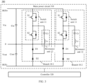
- FIG. 3 is a schematic diagram of a structure of a two-level RSCC 300 according to an embodiment of this application.
- the RSCC 300 includes a main power circuit 310 and a controller 320.
- the main power circuit 310 is a two-level circuit topology. It should be understood that, in FIG. 3 , an example in which the main power circuit 310 includes two RSC branches (that is, a branch 10-1 and a branch 10-2) is only used for description. However, the RSCC shown in FIG. 3 may alternatively include three or more same or different branches.
- the main power circuit 310 includes an input capacitor Cin, an output capacitor Cout, and the branches 10-1 and 10-2.
- Two terminals of the input capacitor Cin are respectively connected to two terminals of input terminals of the main power circuit 310, that is, a BUS+ terminal and a 0 terminal in FIG. 3
- two terminals of the output capacitor Cout are respectively connected to two terminals of output terminals of the main power circuit 310, that is, the 0 terminal and a BUS- terminal in FIG. 3
- the branch 10-1 and the branch 10-2 each include a switch unit 11, a resonance unit 12, a diode D1 (that is, a first diode), and a diode D2 (that is, a second diode).
- the switch unit 11 includes two power switch devices S1 (that is, a first switch) and S2 (that is, a second switch), and the resonance unit 12 includes a resonant capacitor Cr and a resonant inductor Lr that are connected in series.
- a first terminal of the switch S1 is connected to a first terminal of the input capacitor Cin
- a second terminal of the switch S1 is connected to a first terminal of the switch S2 and a first terminal of the resonance unit 12
- a second terminal of the switch S2 is connected to a second terminal of the input capacitor.
- a second terminal of the resonance unit 12 is connected to an anode of D1 and a cathode of D2
- a cathode of D1 is connected to a first terminal of the output capacitor Cout
- an anode of D2 is connected to a second terminal of the output capacitor Cout.
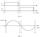
- FIG. 4 shows a control time sequence of a controller 320 for a switch in a switch unit 11 in a main power circuit 310.
- S1, S2, S3, and S4 are all in an off state.
- S1 is turned on, and S2 remains unchanged.
- S1 is continuously on, and S2 is continuously off.
- S1 is turned off.
- S2 is turned on.
- S1 is continuously off, and S2 is continuously on.
- S2 is turned off.
- the main power circuit 310 returns to an initial stage.
- t 1 -t 4 may be referred to as one resonant switching period.
- the controller 320 may control an on state of the switch unit 11 in the main power circuit 310, so that any resonance unit x can obtain electric energy from the input capacitor Cin in a charging stage, and output the electric energy to the output capacitor Cout in a discharging stage.
- FIG. 5 is a schematic diagram of a change in an instantaneous current flowing through a resonance unit 12 in a branch 10-1 in one resonant switching period. It can be learned from FIG. 4 and FIG. 5 that, in the charging stage and the discharging stage, directions of instantaneous currents flowing through the resonance unit in the branch 10-1 are opposite.
- a length of the time period t 1 -t 2 in which the switch S1 is on determines a charging time length of the resonant capacitor Cr
- a length of the time period t 3 -t 4 in which the switch S2 is on determines a discharging time length of the resonant capacitor Cr. Therefore, S1 may also be referred to as a charging switch.
- S2 When S1 is on, the branch 10-1 is in the charging stage.
- S2 may also be referred to as a discharging switch.
- the branch 10-1 is in the discharging stage.
- the branch 10-1 is used as an example for description.
- a control time sequence of a switch in the switch unit 11 and a change in an instantaneous current of the resonance unit 12 are the same as those of the branch 10-1.
- control content of the switch units 11 of the branch 10-1 and the branch 10-2 at a same moment is not necessarily the same.
- the branch 10-1 may be in the charging stage, and the branch 10-2 may be in a discharging stage.
- the controller 320 may collect instantaneous currents flowing through two resonance units 12 in one resonant switching period, and determine characteristic currents of the two resonance units based on the instantaneous currents of the resonance units 12.
- the characteristic current may be a peak value of an instantaneous current in one resonant switching period, or may be a valid value. Further, an arithmetic average value of the characteristic currents is calculated based on the characteristic currents of the N resonance units.
- the branch 10-1 is used as an example. If determining that the characteristic current of the resonance unit 12 is greater than the average value, the controller 320 may be configured to reduce a duty cycle of a control signal of the switch S1 in the branch 10-1. Specifically, as shown in FIG. 4 and FIG. 5 , a turn-off moment of S1 may be advanced to t 2 ', so that a time period in which the branch 10-1 is in the charging stage is reduced, and in a next resonant switching period, the characteristic current of the resonance unit 12 is reduced. Therefore, a stress and loss withstood by the switch in the switch unit 11 are reduced.
- the controller 220 may be configured to reduce a duty cycle of a control signal of the switch S2. Specifically, as shown in FIG. 4 and FIG. 5 , a turn-off moment of S2 may be advanced to t 4 ', so that a time period in which a branch in which the resonance unit 12 is located is in a discharging stage is reduced, and in a next resonant switching period, the characteristic current of the resonance unit 12 is increased. Therefore, a stress and loss withstood by the switch in the switch unit 11 tend to be uniform. For other branches, a case is similar, and details are not described herein again.
- the resonant switched capacitor converter RSCC provided in this application can make currents of parallel branches in the RSCC uniform, so that a stress and a loss of a switch of each branch are uniform, to prevent a circuit fault caused by a too high stress and loss withstood by a switch in some branches.
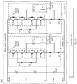
- FIG. 6 is a schematic diagram of a structure of a neutral point clamped (neutral point clamped, NPC)-type three-level RSCC 400 according to an embodiment of this application.
- the RSCC 400 includes a main power circuit 410 and a controller 420, and the main power circuit 410 is an NPC-type three-level topology.
- the main power circuit 410 includes two RSC branches (that is, a branch 20-1 and a branch 20-2) is only used for description.
- the RSCC shown in FIG. 6 may alternatively include three or more same or different branches.
- the main power circuit 410 includes input capacitors C1 (that is, a first capacitor) and C2 (that is, a second capacitor), an output capacitor Cout, and branches 20-1 and 20-2.
- Two terminals of the input capacitors C1 and C2 that are connected in series are respectively connected to two terminals of input terminals of the main power circuit 410, that is, a BUS+ terminal and a 0 terminal in FIG. 6
- two terminals of the output capacitor Cout are respectively connected to two terminals of output terminals of the main power circuit 410, that is, the 0 terminal and a BUS- terminal in FIG. 6 .
- the branch 20-1 and the branch 20-2 each include a switch unit 21, a resonance unit 22, and diodes D1 (that is, a first diode), D2 (that is, a second diode), D3 (that is, a third diode), and D4 (that is, a fourth diode).
- the switch unit 21 includes four power switch devices S1 (that is, a first switch), S2 (that is, a second switch), S3 (that is, a third switch), and S4 (that is, a fourth switch).
- the resonance unit 22 includes a resonant capacitor Cr and a resonant inductor Lr that are connected in series.
- a first terminal of the switch S1 is connected to a first terminal of the first capacitor C1
- a second terminal of the switch S1 is connected to a first terminal of the switch S2 and a cathode of D3
- a second terminal of the switch S2 is connected to a first terminal of the switch S3 and a first terminal of the resonance unit 22
- a second terminal of the switch S3 is connected to a first terminal of the switch S4 and an anode of D4
- a second terminal of the switch S4 is connected to a second terminal of the second capacitor C2
- a first terminal of the second capacitor C2 is connected to a second terminal of the first capacitor C1, an anode of D3, and a cathode of D4.
- a second terminal of the resonance unit is connected to an anode of D1 and a cathode of D2, a cathode of D1 is connected to a first terminal of the output capacitor Cout, and an anode of D2 is connected to a second terminal of the output capacitor Cout.
- FIG. 7 shows a control time sequence of a controller 420 for a switch in a switch unit 21 in a main power circuit 410.
- S1, S2, and S4 are in an off state, and S3 is in an on state.
- S2 is turned on.
- S3 is turned off.
- S1 is turned on.
- S1 is turned off.
- S3 is turned on.
- S4 is turned on.
- S4 is turned off.
- the circuit returns to the initial state.
- ti-ts may be referred to as one resonant switching period.
- the controller 420 may control an on state of the switch unit 21 in the main power circuit 410, so that any resonance unit x can obtain electric energy from the input capacitor Cin in a charging stage, and output the electric energy to the output capacitor Cout in a discharging stage.
- FIG. 8 is a schematic diagram of a change in an instantaneous current flowing through a resonance unit 22 in a branch 20-1 in one resonant switching period. It can be learned from FIG. 7 and FIG. 8 that, in the charging stage and the discharging stage, directions of instantaneous currents flowing through the resonance unit in the branch 20-1 are opposite.
- a length of a time period t 3 -t 4 in which the switch S1 is on determines a charging time length of the resonant capacitor
- a length of a time period t 7 -t 8 in which the switch S4 is on determines a discharging time length of the resonant capacitor. Therefore, S1 may also be referred to as a charging switch.
- S4 When S1 is on, the branch 21-1 is in a charging stage.
- S4 may also be referred to as a discharging switch.
- the branch 21-1 is in a discharging stage.
- the branch 20-1 is used as an example for description.
- a control time sequence of a switch in the switch unit 21 and a change in an instantaneous current of the resonance unit 22 are the same as those of the branch 20-1.
- control content of the switch units 21 of the branch 20-1 and the branch 20-2 at a same moment is not necessarily the same.
- the branch 20-1 may be in the charging stage, and the branch 20-2 may be in a discharging stage.
- the controller 420 may collect instantaneous currents flowing through two resonance units 22 in one resonant switching period, and determine characteristic currents of the two resonance units based on the instantaneous currents of the resonance units 22.
- the characteristic current may be a peak value of an instantaneous current in one resonant switching period, or may be a valid value. Further, an arithmetic average value of the characteristic currents is calculated based on the characteristic currents of the N resonance units.
- the branch 20-1 is used as an example. If determining that the characteristic current of the resonance unit 22 is greater than the average value, the controller 420 may be configured to reduce a duty cycle of a control signal of the switch S1 in the branch 20-1. Specifically, as shown in FIG. 7 and FIG. 8 , a turn-off moment of S1 may be advanced to t 4 ', so that a time period in which the branch 20-1 is in the charging stage is reduced, and in a next resonant switching period, the characteristic current of the resonance unit 22 is reduced. Therefore, a stress and loss withstood by the switch in the switch unit 21 are reduced.
- the controller 220 may be configured to reduce a duty cycle of a control signal of the switch S4. Specifically, as shown in FIG. 7 and FIG. 8 , a turn-off moment of S4 may be advanced to t 8 ', so that a time period in which a branch in which the resonance unit 22 is located is in a discharging stage is reduced, and in a next resonant switching period, the characteristic current of the resonance unit 22 is increased. Therefore, a stress and loss withstood by the switch in the switch unit 21 tend to be uniform. For other branches, a case is similar, and details are not described herein again.
- the resonant switched capacitor converter RSCC provided in this application can make currents of parallel branches in the RSCC uniform, so that a stress and a loss of a switch of each branch are uniform, to prevent a circuit fault caused by a too high stress and loss withstood by a switch in some branches.
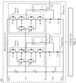
- FIG. 9 is a schematic diagram of a structure of an active neutral point clamped (Active Neutral Point Clamped, ANPC)-type three-level RSCC 500 according to an embodiment of this application.
- the RSCC 500 includes a main power circuit 510 and a controller 520, and the main power circuit 510 is an NPC-type three-level topology.
- the main power circuit 510 includes two RSC branches (that is, a branch 30-1 and a branch 30-2) is only used for description.
- the RSCC shown in FIG. 9 may alternatively include three or more same or different branches.
- the main power circuit 510 includes input capacitors C1 (that is, a first capacitor) and C2 (that is, a second capacitor), an output capacitor Cout, and branches 30-1 and 30-2.
- Two terminals of the input capacitors C1 and C2 that are connected in series are respectively connected to two terminals of input terminals of the main power circuit 510, that is, a BUS+ terminal and a 0 terminal in FIG. 9
- two terminals of the output capacitor Cout are respectively connected to two terminals of output terminals of the main power circuit 510, that is, the 0 terminal and a BUS- terminal in FIG. 9 .
- the branch 30-1 and the branch 30-2 each include a switch unit 31, a resonance unit 32, and diodes D1 (that is, a first diode) and D2 (that is, a second diode).
- the switch unit 31 includes two power switch devices S1 (that is, a first switch) and S2 (that is, a second switch), and the resonance unit 12 includes a resonant capacitor Cr and a resonant inductor Lr that are connected in series.
- a first terminal of the switch S1 is connected to a first terminal of the first capacitor C1
- a second terminal of the switch S1 is connected to a first terminal of the switch S2 and a first terminal of the switch S5
- a second terminal of the switch S2 is connected to a first terminal of the switch S3 and a first terminal of the resonance unit 32
- a second terminal of the switch S3 is connected to a first terminal of the switch S4 and a second terminal of the switch S6
- a second terminal of the switch S4 is connected to a second terminal of the second capacitor C2
- a first terminal of the second capacitor C2 is connected to a second terminal of the first capacitor C1, a second terminal of the switch S5, and a first terminal of the switch S6.
- a second terminal of the resonance unit 32 is connected to an anode of D1 and a cathode of D2, a cathode of D1 is connected to a first terminal of the output capacitor Cout, and an anode of D2 is connected to a second terminal of the output capacitor Cout.
- FIG. 10 shows a control time sequence of a controller 520 for a switch in a switch unit 31 in a main power circuit 510.
- S1, S2, S4, and S6 are in an off state, and S3 and S5 are in an on state.
- S5 is turned off, and S6 is turned on.
- S2 is turned on, and S3 is turned off.
- S1 is turned on.
- S1 is turned off.
- S6 is turned off.
- S2 is turned off, and S3 is turned on.
- S4 is turned on.
- S4 is turned off, and the circuit returns to an initial state.
- ti-ts may be referred to as one resonant switching period.
- a current flow direction is the BUS+ terminal, S1, S2, the resonance unit 32, D1, and the 0 terminal, the branch 30-1 is in a charging state, and the input capacitors C1 and C2 charge the resonant capacitor Cr.
- a current flow direction is the resonance unit 32, S3, S4, the 0 terminal, Cout, the BUS- terminal, and D2, the branch 30-1 is in a discharging state, and the resonant capacitor Cr is used as a power supply to charge the output capacitor Cout.
- the controller 520 may control an on state of the switch unit 31 in the main power circuit 510, so that any resonance unit x can obtain electric energy from the input capacitor Cin in a charging stage, and output the electric energy to the output capacitor Cout in a discharging stage.
- FIG. 11 is a schematic diagram of a change in an instantaneous current flowing through a resonance unit 32 in a branch 30-1 in one resonant switching period. It can be learned from FIG. 11 that, in the charging stage and the discharging stage, directions of instantaneous currents flowing through the resonance unit in the branch 30-1 are opposite. A length of a time period t 3 -t 4 in which the switch S1 is on determines a charging time length of the resonant capacitor, and a length of a time period t 7 -t 8 in which the switch S4 is on determines a discharging time length of the resonant capacitor. Therefore, S1 may also be referred to as a charging switch. When S1 is on, the branch 30-1 is in the charging stage. S4 may also be referred to as a discharging switch. When S4 is on, a branch 10 is in the discharging stage.
- the branch 30-1 is used as an example for description.
- a control time sequence of a switch in the switch unit 31 and a change in an instantaneous current of the resonance unit 32 are the same as those of the branch 30-1.
- control content of the switch units 31 of the branch 30-1 and the branch 30-2 at a same moment is not necessarily the same.
- the branch 30-1 may be in the charging stage, and the branch 30-2 may be in a discharging stage.
- the controller 520 may collect instantaneous currents flowing through two resonance units 32 in one resonant switching period, and determine characteristic currents of the two resonance units based on the instantaneous currents of the resonance units 32.
- the characteristic current may be a peak value of an instantaneous current in one resonant switching period, or may be a valid value. Further, an arithmetic average value of the characteristic currents is calculated based on the characteristic currents of the N resonance units.
- the branch 30-1 is used as an example. If determining that the characteristic current of the resonance unit 32 is greater than the average value, the controller 520 may be configured to reduce a duty cycle of a control signal of the switch S1 in the branch 30-1. Specifically, as shown in FIG. 10 and FIG. 11 , a turn-off moment of S1 may be advanced to t 4 ', so that a time period in which the branch 30-1 is in the charging stage is reduced, and in a next resonant switching period, the characteristic current of the resonance unit 32 is reduced. Therefore, a stress and loss withstood by the switch in the switch unit 31 are reduced.
- the controller 220 may be configured to reduce a duty cycle of a control signal of the switch S4. Specifically, as shown in FIG. 10 and FIG. 11 , a turn-off moment of S4 may be advanced to t 8 ', so that a time period in which a branch in which the resonance unit 32 is located is in a discharging stage is reduced, and in a next resonant switching period, the characteristic current of the resonance unit 32 is increased. Therefore, a stress and loss withstood by the switch in the switch unit 31 tend to be uniform. For other branches, a case is similar, and details are not described herein again.
- the resonant switched capacitor converter RSCC provided in this application can make currents of parallel branches in the RSCC uniform, so that a stress and a loss of a switch of each branch are uniform, to prevent a circuit fault caused by a too high stress and loss withstood by a switch in some branches.
- N parallel branches in an RSCC may be completely the same or may be different.
- RSC branches with different topologies may be connected in parallel to a main power circuit.
- the input capacitor of the main power circuit 210 in FIG. 2 may include two capacitors C1 and C2, a topology of an RSC branch 1 may be shown as the branch 10-1 in FIG. 3 , a topology of an RSC branch 2 may be shown as the branch 20-1 in FIG. 6 , and a topology of an RSC branch 3 may be shown as the branch 30 in FIG. 9 . This is not limited in this embodiment of this application.
- functions of the controller 220, the controller 320, the controller 420, and the controller 520 each may be separately implemented by a sampling unit and a control unit.
- the sampling unit may be specifically configured to: collect instantaneous current information of instantaneous currents flowing through N resonance units in one resonant switching period, and send the instantaneous current information of the N resonance units to the control unit.
- the control unit may be specifically configured to: receive the instantaneous current information of the N resonance units, determine characteristic currents of the N resonance units based on the instantaneous current information of the N resonance units, and calculate an arithmetic average value of the characteristic currents based on the characteristic currents of the N resonance units.
- the characteristic current is a valid value or a peak value of an instantaneous current flowing through the resonance unit in one resonant switching period, and the valid value may be calculated based on the peak value.
- a specific calculation manner is multiplying the peak value by a square root of 2.
- the average value may be obtained by dividing a sum of N valid values or peak values by a total quantity N.
- the resonant switched capacitor converter includes an input capacitor, an output capacitor, N parallel resonant switched capacitor branches, and a controller.
- Each of the N resonant switched capacitor branches includes a switch unit and a resonance unit.
- the controller may control an on state of a switch in the switch unit, so that the resonance unit obtains electric energy from the input capacitor in a charging stage, and the resonance unit outputs the electric energy to the output capacitor in a discharging stage.
- the method includes: The controller determines an average value of characteristic currents of N resonance units.
- the N resonance units are in a one-to-one correspondence with the N resonant switched capacitor branches, and the characteristic current is a valid value or a peak value of an instantaneous current of the resonance unit in one resonant switching period.
- the controller reduces a duty cycle of a control signal of a charging switch in a first switch unit when determining that a characteristic current of a first resonance unit is greater than the average value.
- a branch corresponding to the charging switch is in a charging stage when the charging switch is turned on.
- the controller reduces a duty cycle of a control signal of a discharging switch in the first switch unit when determining that the characteristic current of the first resonance unit is less than the average value.
- a branch corresponding to the discharging switch is in a discharging stage when the discharging switch is turned on.
- the first resonance unit is any one of the N resonance units, and the first switch unit is a switch unit in a resonant switched capacitor branch in which the first resonance unit is located, where N is an integer greater than 1.
- the resonant switched capacitor converter RSCC provided in this application can make currents of parallel branches in the RSCC uniform, so that a stress and a loss of a switch of each branch are uniform, to prevent a circuit fault caused by a too high stress and loss withstood by a switch in some branches.
- controller reduces a duty cycle of a control signal of a charging switch in a first switch unit when determining that a characteristic current of a first resonance unit is greater than the average value includes: The controller reduces the duty cycle of the control signal of the charging switch when determining that the characteristic current of the first resonance unit is greater than the average value and a difference between the current of the first resonance unit and the average value is greater than a first threshold.
- controller reduces a duty cycle of a control signal of a discharging switch in the first switch unit when determining that the characteristic current of the first resonance unit is less than the average value includes: The controller reduces the duty cycle of the control signal of the discharging switch when determining that the characteristic current of the first resonance unit is less than the average value and a difference between the current of the first resonance unit and the average value is greater than a second threshold.
- the controller determines an average value of characteristic currents of N resonance units includes: The controller detects instantaneous currents of the N resonance units; the controller determines the characteristic currents of the N resonance units based on the instantaneous currents of the N resonance units; and the controller calculates the average value based on the characteristic currents of the N resonance units.
- the controller includes a sampling unit and a control unit, and that the controller determines an average value of characteristic currents of N resonance units includes:
- the sampling unit collects instantaneous current information of the N resonance units, and sends the instantaneous current information of the N resonance units to the control unit; and the control unit receives the instantaneous current information of the N resonance units, and determines a valid value of each of the currents of the N resonance units and the average value based on the instantaneous current information of the N resonance units.
- the resonant switched capacitor converter is a two-level resonant switched capacitor converter
- the resonance unit includes a resonant capacitor and a resonant inductor that are connected in series
- the switch unit includes a first switch and a second switch
- the first switch is the charging switch
- the second switch is the discharging switch
- each of the N resonant switched capacitor branches further includes a first diode and a second diode
- a first terminal of the first switch is connected to a first terminal of the input capacitor
- a second terminal of the first switch is connected to a first terminal of the second switch and a first terminal of the resonance unit
- a second terminal of the second switch is connected to a second terminal of the input capacitor
- a second terminal of the resonance unit is connected to an anode of the first diode and a cathode of the second diode, a cathode of the first diode is connected to a first terminal of the output capacitor, and an anode of the second di
- the resonant switched capacitor converter is a neutral point clamped NPC-type three-level resonant switched capacitor converter
- the resonance unit includes a resonant capacitor and a resonant inductor that are connected in series
- the input capacitor includes a first capacitor and a second capacitor
- the switch unit includes a first switch, a second switch, a third switch, and a fourth switch
- the first switch is the charging switch
- the fourth switch is the discharging switch
- each of the N resonant switched capacitor branches further includes a first diode, a second diode, a third diode, and a fourth diode
- a first terminal of the first switch is connected to a first terminal of the first capacitor
- a second terminal of the first switch is connected to a first terminal of the second switch and a cathode of the third diode
- a second terminal of the second switch is connected to a first terminal of the third switch and a first terminal of the resonance unit
- the resonant switched capacitor converter is an active neutral point clamped ANPC-type three-level resonant switched capacitor converter
- the resonance unit includes a resonant capacitor and a resonant inductor that are connected in series
- the input capacitor includes a first capacitor and a second capacitor
- the switch unit includes a first switch, a second switch, a third switch, a fourth switch, a fifth switch, and a sixth switch
- the first switch is the charging switch
- the fourth switch is the discharging switch
- each of the N resonant switched capacitor branches further includes a first diode and a second diode; a first terminal of the first switch is connected to a first terminal of the first capacitor, a second terminal of the first switch is connected to a first terminal of the second switch and a first terminal of the fifth switch, a second terminal of the second switch is connected to a first terminal of the third switch and a first terminal of the resonance unit, a second terminal of the third switch is connected to a first terminal of the
- FIG. 12 is a schematic diagram of a control method for a resonant switched capacitor converter according to this application. The following describes a control method for an RSCC in this application with reference to FIG. 12 .
- S620 Determine characteristic currents of the N resonance units based on the instantaneous currents of the N resonance units.
- S640 Reduce a duty cycle of a control signal of a charging switch in a first switch unit when determining that a characteristic current of a first resonance unit is greater than the average value, where a branch in which the charging switch is located is in a charging stage when the charging switch is turned on.
- S650 Reduce a duty cycle of a control signal of a discharging switch in a first switch unit when determining that a characteristic current of a first resonance unit is less than the average value, where a branch in which the discharging switch is located is in a discharging stage when the discharging switch is turned on.
- FIG. 13 is a schematic diagram of a structure of a control device 700 according to an embodiment of this application.
- the control device 700 includes a processor 710 and a communication interface 720.
- the control device 700 may further include a memory 730.
- the memory 730 may be included in the processor 710.
- the processor 710, the communication interface 720, and the memory 730 communicate with each other through an internal connection path.
- the memory 730 is configured to store instructions.
- the processor 710 is configured to execute the instructions stored in the memory 730, to implement the control method provided in embodiments of this application.
- the control device 700 may be configured to implement a function of a controller in FIG. 2 , FIG. 3 , FIG. 6 , or FIG. 9 , or implement a function of each control unit in FIG. 2 , FIG. 3 , FIG. 6 , or FIG. 9 .
- this application further provides an MPPT combiner box, including the foregoing resonant switched converter capacitor RSCC.
- this application further provides a power supply system, including the foregoing resonant switched converter capacitor RSCC.
- ком ⁇ онент may be but is not limited to a process that runs on a processor, the processor, an object, an executable file, an execution thread, a program, and/or a computer.
- a computing device and an application that runs on the computing device may be components.
- One or more components may reside within the process and/or the execution thread, and the component may be located on one computer and/or distributed between two or more computers.
- these components may be executed by various computer-readable media that store various data structures.
- the components may communicate by using a local and/or remote process and based on a signal having one or more data packets (for example, data from two components interacting with another component in a local system, a distributed system, and/or across a network such as the internet interacting with another system by using the signal).
- a signal having one or more data packets (for example, data from two components interacting with another component in a local system, a distributed system, and/or across a network such as the internet interacting with another system by using the signal).
- the disclosed system, apparatus, and method may be implemented in other manners.
- the described apparatus embodiments are merely examples.
- division into the units is merely logical function division and may be other division in an actual implementation.
- a plurality of units or components may be combined or integrated into another system, or some features may be ignored or not performed.
- the displayed or discussed mutual couplings or direct couplings or communication connections may be implemented through some interfaces.
- the indirect couplings or communication connections between the apparatuses or units may be implemented in an electronic, mechanical, or another form.
- the units described as separate parts may or may not be physically separate, and parts displayed as units may or may not be physical units, and may be located in one place, or may be distributed on a plurality of network units. Some or all of the units may be selected based on an actual requirement, to achieve the objectives of the solutions of embodiments.
- the functions When the functions are implemented in a form of a software functional unit and sold or used as an independent product, the functions may be stored in a computer-readable storage medium. Based on such an understanding, the technical solutions of this application essentially, or the part contributing to the conventional technology, or some of the technical solutions may be implemented in a form of a software product.
- the software product is stored in a storage medium, and includes several instructions for instructing a computer device (which may be a personal computer, a server, or a network device) to perform all or some of the steps of the methods described in embodiments of this application.
- the foregoing storage medium includes any medium that can store program code, for example, a USB flash drive, a removable hard disk, a read-only memory (Read-Only Memory, ROM), a random access memory (Random Access Memory, RAM), a magnetic disk, or a compact disc.
- a USB flash drive for example, a USB flash drive, a removable hard disk, a read-only memory (Read-Only Memory, ROM), a random access memory (Random Access Memory, RAM), a magnetic disk, or a compact disc.
Landscapes
- Engineering & Computer Science (AREA)
- Power Engineering (AREA)
- Dc-Dc Converters (AREA)
Abstract
Description
- This application claims priority to
Chinese Patent Application No. 202110573323.X, filed on May 25, 2021 - This application relates to the circuit field, and more specifically, to a resonant switched capacitor converter and a control method thereof.
- As photovoltaic power generation, an electric vehicle, and a renewable energy system have more requirements for a power electronic converter. Most conventional direct current converters transfer energy by using a magnetic element, for example, an inductor or a transformer, and have a large volume and a low power density. In addition, most of these converters work in a hard switching state, and have a high switching loss and low efficiency.
- Compared with a conventional switched capacitor converter, a resonant switched capacitor converter (resonant switched capacitor converter, RSCC) transfers energy by using a resonance unit (a resonant inductor and a resonant capacitor), to reduce a volume of the converter. In addition, both a charging capacitor and a discharging capacitor of the resonant switched capacitor converter work in a resonant state. Therefore, a current spike problem does not occur, and the resonant switched capacitor converter may be applied to a scenario in which an output current is large.
- When the RSCC includes a plurality of parallel branches, a conversion power of the RSCC may be increased. However, due to different circuit parameters, currents of the branches in the RSCC may be not uniform, affecting a stress and a loss of a power switch device in the RSCC.
- This application provides a resonant switched capacitor converter and a control method thereof, to make currents of parallel branches in the RSCC uniform, so that a stress and a loss of a switch of each branch are uniform.
- According to a first aspect, a resonant switched capacitor converter is provided, including: an input capacitor and an output capacitor; N parallel resonant switched capacitor branches, where each of the N resonant switched capacitor branches includes a switch unit and a resonance unit; and a controller, where the controller is configured to control an on state of a switch in the switch unit, so that the resonance unit obtains electric energy from the input capacitor in a charging stage, and the resonance unit outputs the electric energy to the output capacitor in a discharging stage. The controller is further configured to: determine an average value of characteristic currents of N resonance units, where the N resonance units are in a one-to-one correspondence with the N resonant switched capacitor branches, and the characteristic current is a valid value or a peak value of an instantaneous current of the resonance unit in one resonant switching period; and reduce a duty cycle of a control signal of a charging switch in a first switch unit when determining that a characteristic current of a first resonance unit is greater than the average value, where a resonant switched capacitor branch corresponding to the charging switch is in a charging stage when the charging switch is turned on; or reduce a duty cycle of a control signal of a discharging switch in the first switch unit when determining that the characteristic current of the first resonance unit is less than the average value, where a resonant switched capacitor branch corresponding to the discharging switch is in a discharging stage when the discharging switch is turned on. The first resonance unit is any one of the N resonance units, and the first switch unit is a switch unit in a resonant switched capacitor branch in which the first resonance unit is located, where N is an integer greater than 1.
- Specifically, the controller may determine a valid value or a peak value of an instantaneous current flowing through each of the N resonance units in one resonant switching period. The valid value or the peak value may also be referred to as a characteristic current, and an average value of N characteristic currents is further calculated. The average value may be understood as a standard current withstood by each resonance unit. When it is determined that the characteristic current of the first resonance unit is greater than the average value, it indicates that a current withstood by a switch in the first switch unit is greater than the standard current, and the controller may be configured to reduce the duty cycle of the control signal of the charging switch. In this manner, a time period in which a branch in which the first resonance unit is located is in a charging stage is reduced, and the characteristic current of the first resonance unit is reduced in a next resonant switching period, so that a stress and a loss withstood by the switch in the first switch unit are reduced. When it is determined that the characteristic current of the first resonance unit is less than the average value, it indicates that a current flowing through a switch in the first switch unit is less than the standard current, and the controller may be configured to reduce the duty cycle of the control signal of the discharging switch. In this manner, a time period in which a branch in which the first resonance unit is located is in a discharging stage is reduced, and the characteristic current of the first resonance unit is increased in a next resonant switching period, so that a stress and a loss withstood by the switch in the first switch unit tend to be uniform.
- Therefore, the resonant switched capacitor converter RSCC provided in this application can make currents of parallel branches in the RSCC uniform, so that a stress and a loss of a switch of each branch are uniform, to prevent a circuit fault caused by a too high stress and loss withstood by a switch in some branches.
- With reference to the first aspect, in a possible implementation, the controller is specifically configured to: reduce the duty cycle of the control signal of the charging switch when determining that the characteristic current of the first resonance unit is greater than the average value and a difference between the characteristic current of the first resonance unit and the average value is greater than a first threshold; or reduce the duty cycle of the control signal of the discharging switch when determining that the characteristic current of the first resonance unit is less than the average value and a difference between the characteristic current of the first resonance unit and the average value is greater than a second threshold.
- With reference to the first aspect, in a possible implementation, the controller is specifically configured to: detect instantaneous currents of the N resonance units; determine the characteristic currents of the N resonance units based on the instantaneous currents of the N resonance units; and calculate the average value based on the characteristic currents of the N resonance units.
- With reference to the first aspect, in a possible implementation, the controller includes a sampling unit and a control unit; the sampling unit is specifically configured to: collect instantaneous current information of the N resonance units, and send the instantaneous current information of the N resonance units to the control unit; and the control unit is specifically configured to: receive the instantaneous current information of the N resonance units; determine the characteristic currents of the N resonance units based on the instantaneous current information of the N resonance units; and calculate the average value based on the characteristic currents of the N resonance units.
- With reference to the first aspect, in a possible implementation, the resonant switched capacitor converter is a two-level resonant switched capacitor converter, the resonance unit includes a resonant capacitor and a resonant inductor that are connected in series, the switch unit includes a first switch and a second switch, the first switch is the charging switch, the second switch is the discharging switch, and each of the N resonant switched capacitor branches further includes a first diode and a second diode; a first terminal of the first switch is connected to a first terminal of the input capacitor, a second terminal of the first switch is connected to a first terminal of the second switch and a first terminal of the resonance unit, and a second terminal of the second switch is connected to a second terminal of the input capacitor; and a second terminal of the resonance unit is connected to an anode of the first diode and a cathode of the second diode, a cathode of the first diode is connected to a first terminal of the output capacitor, and an anode of the second diode is connected to a second terminal of the output capacitor.
- With reference to the first aspect, in a possible implementation, the resonant switched capacitor converter is a neutral point clamped NPC-type three-level resonant switched capacitor converter, the resonance unit includes a resonant capacitor and a resonant inductor that are connected in series, the input capacitor includes a first capacitor and a second capacitor, the switch unit includes a first switch, a second switch, a third switch, and a fourth switch, the first switch is the charging switch, the fourth switch is the discharging switch, and each of the N resonant switched capacitor branches further includes a first diode, a second diode, a third diode, and a fourth diode; a first terminal of the first switch is connected to a first terminal of the first capacitor, a second terminal of the first switch is connected to a first terminal of the second switch and a cathode of the third diode, a second terminal of the second switch is connected to a first terminal of the third switch and a first terminal of the resonance unit, a second terminal of the third switch is connected to a first terminal of the fourth switch and an anode of the fourth diode, a second terminal of the fourth switch is connected to a second terminal of the second capacitor, a first terminal of the second capacitor is connected to a second terminal of the first capacitor, an anode of the third diode, and a cathode of the fourth diode; and a second terminal of the resonance unit is connected to an anode of the first diode and a cathode of the second diode, a cathode of the first diode is connected to a first terminal of the output capacitor, and an anode of the second diode is connected to a second terminal of the output capacitor.
- With reference to the first aspect, in a possible implementation, the resonant switched capacitor converter is an active neutral point clamped ANPC-type three-level resonant switched capacitor converter, the resonance unit includes a resonant capacitor and a resonant inductor that are connected in series, the input capacitor includes a first capacitor and a second capacitor, the switch unit includes a first switch, a second switch, a third switch, a fourth switch, a fifth switch, and a sixth switch, the first switch is the charging switch, the fourth switch is the discharging switch, and each of the N resonant switched capacitor branches further includes a first diode and a second diode; a first terminal of the first switch is connected to a first terminal of the first capacitor, a second terminal of the first switch is connected to a first terminal of the second switch and a first terminal of the fifth switch, a second terminal of the second switch is connected to a first terminal of the third switch and a first terminal of the resonance unit, a second terminal of the third switch is connected to a first terminal of the fourth switch and a second terminal of the sixth switch, a second terminal of the fourth switch is connected to a second terminal of the second capacitor, and a first terminal of the second capacitor is connected to a second terminal of the first capacitor, a second terminal of the fifth switch, and a first terminal of the sixth switch; and a second terminal of the resonance unit is connected to an anode of the first diode and a cathode of the second diode, a cathode of the first diode is connected to a first terminal of the output capacitor, and an anode of the second diode is connected to a second terminal of the output capacitor.
- According to a second aspect, a control method for a resonant switched capacitor converter is provided. The resonant switched capacitor converter includes: an input capacitor and an output capacitor; N parallel resonant switched capacitor branches, where each of the N resonant switched capacitor branches includes a switch unit and a resonance unit; and a controller, where the controller is configured to control an on state of a switch in the switch unit, so that the resonance unit obtains electric energy from the input capacitor in a charging stage, and the resonance unit outputs the electric energy to the output capacitor in a discharging stage. The method includes: The controller determines an average value of characteristic currents of N resonance units. The N resonance units are in a one-to-one correspondence with the N resonant switched capacitor branches, and the characteristic current is a valid value or a peak value of an instantaneous current of the resonance unit in one resonant switching period. The controller reduces a duty cycle of a control signal of a charging switch in a first switch unit when determining that a characteristic current of a first resonance unit is greater than the average value. A resonant switched capacitor branch corresponding to the charging switch is in a charging stage when the charging switch is turned on. Alternatively, the controller reduces a duty cycle of a control signal of a discharging switch in the first switch unit when determining that the characteristic current of the first resonance unit is less than the average value. A resonant switched capacitor branch corresponding to the discharging switch is in a discharging stage when the discharging switch is turned on. The first resonance unit is any one of the N resonance units, and the first switch unit is a switch unit in a resonant switched capacitor branch in which the first resonance unit is located, where N is an integer greater than 1.
- Specifically, the controller may determine a valid value or a peak value of an instantaneous current flowing through each of the N resonance units in one resonant switching period. The valid value or the peak value may also be referred to as a characteristic current, and an average value of N characteristic currents is further calculated. The average value may be understood as a standard current withstood by each resonance unit. When it is determined that the characteristic current of the first resonance unit is greater than the average value, it indicates that a current withstood by a switch in the first switch unit is greater than the standard current, and the controller may be configured to reduce the duty cycle of the control signal of the charging switch. In this manner, a time period in which a branch in which the first resonance unit is located is in a charging stage is reduced, and the characteristic current of the first resonance unit is reduced in a next resonant switching period, so that a stress and a loss withstood by the switch in the first switch unit are reduced. When it is determined that the characteristic current of the first resonance unit is less than the average value, it indicates that a current flowing through a switch in the first switch unit is less than the standard current, and the controller may be configured to reduce the duty cycle of the control signal of the discharging switch. In this manner, a time period in which a branch in which the first resonance unit is located is in a discharging stage is reduced, and the characteristic current of the first resonance unit is increased in a next resonant switching period, so that a stress and a loss withstood by the switch in the first switch unit tend to be uniform.
- Therefore, the resonant switched capacitor converter RSCC provided in this application can make currents of parallel branches in the RSCC uniform, so that a stress and a loss of a switch of each branch are uniform, to prevent a circuit fault caused by a too high stress and loss withstood by a switch in some branches.
- With reference to the second aspect, in a second possible implementation, that the controller reduces a duty cycle of a control signal of a charging switch in a first switch unit when determining that a characteristic current of a first resonance unit is greater than the average value includes: The controller reduces the duty cycle of the control signal of the charging switch when determining that the characteristic current of the first resonance unit is greater than the average value and a difference between the current of the first resonance unit and the average value is greater than a first threshold. That the controller reduces a duty cycle of a control signal of a discharging switch in the first switch unit when determining that the characteristic current of the first resonance unit is less than the average value includes: The controller reduces the duty cycle of the control signal of the discharging switch when determining that the characteristic current of the first resonance unit is less than the average value and a difference between the current of the first resonance unit and the average value is greater than a second threshold.
- With reference to the second aspect, in a second possible implementation, that the controller determines an average value of characteristic currents of N resonance units includes: The controller detects instantaneous currents of the N resonance units; determines the characteristic currents of the N resonance units based on the instantaneous currents of the N resonance units; and calculates the average value based on the characteristic currents of the N resonance units.
- With reference to the second aspect, in a second possible implementation, the controller includes a sampling unit and a control unit, and that the controller determines an average value of characteristic currents of N resonance units includes: The sampling unit collects instantaneous current information of the N resonance units, and sends the instantaneous current information of the N resonance units to the control unit; and the control unit receives the instantaneous current information of the N resonance units, and determines a valid value of each of the currents of the N resonance units and the average value based on the instantaneous current information of the N resonance units.
- With reference to the second aspect, in a second possible implementation, the resonant switched capacitor converter is a two-level resonant switched capacitor converter, the resonance unit includes a resonant capacitor and a resonant inductor that are connected in series, the switch unit includes a first switch and a second switch, the first switch is the charging switch, the second switch is the discharging switch, and each of the N resonant switched capacitor branches further includes a first diode and a second diode; a first terminal of the first switch is connected to a first terminal of the input capacitor, a second terminal of the first switch is connected to a first terminal of the second switch and a first terminal of the resonance unit, and a second terminal of the second switch is connected to a second terminal of the input capacitor; and a second terminal of the resonance unit is connected to an anode of the first diode and a cathode of the second diode, a cathode of the first diode is connected to a first terminal of the output capacitor, and an anode of the second diode is connected to a second terminal of the output capacitor.
- With reference to the second aspect, in a second possible implementation, the resonant switched capacitor converter is a neutral point clamped NPC-type three-level resonant switched capacitor converter, the resonance unit includes a resonant capacitor and a resonant inductor that are connected in series, the input capacitor includes a first capacitor and a second capacitor, the switch unit includes a first switch, a second switch, a third switch, and a fourth switch, the first switch is the charging switch, the fourth switch is the discharging switch, and each of the N resonant switched capacitor branches further includes a first diode, a second diode, a third diode, and a fourth diode; a first terminal of the first switch is connected to a first terminal of the first capacitor, a second terminal of the first switch is connected to a first terminal of the second switch and a cathode of the third diode, a second terminal of the second switch is connected to a first terminal of the third switch and a first terminal of the resonance unit, a second terminal of the third switch is connected to a first terminal of the fourth switch and an anode of the fourth diode, a second terminal of the fourth switch is connected to a second terminal of the second capacitor, a first terminal of the second capacitor is connected to a second terminal of the first capacitor, an anode of the third diode, and a cathode of the fourth diode; and a second terminal of the resonance unit is connected to an anode of the first diode and a cathode of the second diode, a cathode of the first diode is connected to a first terminal of the output capacitor, and an anode of the second diode is connected to a second terminal of the output capacitor.
- With reference to the second aspect, in a second possible implementation, the resonant switched capacitor converter is an active neutral point clamped ANPC-type three-level resonant switched capacitor converter, the resonance unit includes a resonant capacitor and a resonant inductor that are connected in series, the input capacitor includes a first capacitor and a second capacitor, the switch unit includes a first switch, a second switch, a third switch, a fourth switch, a fifth switch, and a sixth switch, the first switch is the charging switch, the fourth switch is the discharging switch, and each of the N resonant switched capacitor branches further includes a first diode and a second diode; a first terminal of the first switch is connected to a first terminal of the first capacitor, a second terminal of the first switch is connected to a first terminal of the second switch and a first terminal of the fifth switch, a second terminal of the second switch is connected to a first terminal of the third switch and a first terminal of the resonance unit, a second terminal of the third switch is connected to a first terminal of the fourth switch and a second terminal of the sixth switch, a second terminal of the fourth switch is connected to a second terminal of the second capacitor, and a first terminal of the second capacitor is connected to a second terminal of the first capacitor, a second terminal of the fifth switch, and a first terminal of the sixth switch; and a second terminal of the resonance unit is connected to an anode of the first diode and a cathode of the second diode, a cathode of the first diode is connected to a first terminal of the output capacitor, and an anode of the second diode is connected to a second terminal of the output capacitor.
- According to a third aspect, a maximum power point tracking MPPT combiner box is provided, including the resonant switched converter capacitor RSCC in any one of the first aspect and the implementations of the first aspect.
- According to a fourth aspect, a power supply system is provided, including the resonant switched converter capacitor RSCC in any one of the first aspect and the implementations of the first aspect.
-
-
FIG. 1 is a schematic block diagram of an application scenario according to this application; -
FIG. 2 is a schematic diagram of a resonant switched capacitor converter RSCC according to this application; -
FIG. 3 is a schematic diagram of a structure of a two-level RSCC according to an embodiment of this application; -
FIG. 4 shows a control time sequence of a switch in a switch unit of a main power circuit in a two-level RSCC; -
FIG. 5 is a schematic diagram of a change in an instantaneous current of a resonance unit in a two-level RSCC in one resonant switching period; -
FIG. 6 is a schematic diagram of a structure of an NPC-type three-level RSCC according to an embodiment of this application; -
FIG. 7 shows a control time sequence of a switch in a switch unit of a main power circuit in an NPC-type three-level RSCC; -
FIG. 8 is a schematic diagram of a change in an instantaneous current of a resonance unit in an NPC-type three-level RSCC in one resonant switching period; -
FIG. 9 is a schematic diagram of a structure of an ANPC-type three-level RSCC according to an embodiment of this application; -
FIG. 10 shows a control time sequence of a switch in a switch unit of a main power circuit in an ANPC-type three-level RSCC; -
FIG. 11 is a schematic diagram of a change in an instantaneous current of a resonance unit in an ANPC-type three-level RSCC in one resonant switching period; -
FIG. 12 is a schematic diagram of a control method for a resonant switched capacitor converter according to this application; and -
FIG. 13 is a schematic diagram of a structure of a control device according to an embodiment of this application. - The following describes technical solutions of this application with reference to accompanying drawings.
-
FIG. 1 is a schematic block diagram of an application scenario according to this application. As shown inFIG. 1 , a resonant switched capacitor converter (resonant switched capacitor converter, RSCC) in this application may be used in apower supply system 100. Thepower supply system 100 may generate electric energy and supply power to a power grid. Specifically, thepower supply system 100 may include apower supply module 110, a maximum power point tracking (maximum power point tracking, MPPT)combiner box 120, and aninverter circuit 130. TheMPPT combiner box 120 may include a direct current-direct current boost circuit 121, a direct current-directcurrent boost circuit 122, and anRSCC 123. A positive output terminal of the direct current-direct current boost circuit 121 is connected to a positive input terminal of theinverter circuit 130, and a negative output terminal of the direct current-direct current boost circuit 121 is connected to a zero-potential input terminal of theinverter circuit 130. A positive output terminal of the direct current-directcurrent boost circuit 122 is connected to a positive input terminal of theRSCC 123, and a negative output terminal of the direct current-directcurrent boost circuit 122 is connected to a negative input terminal of theRSCC 123. A positive output terminal of theRSCC 123 is connected to the zero-potential input terminal of theinverter circuit 130, and a negative output terminal of theRSCC 123 is connected to a negative input terminal of theinverter circuit 130. In other words, theRSCC 123 may convert, into a negative voltage, a positive voltage output by the direct current-directcurrent boost circuit 2, connect in series the negative voltage and a voltage output by the direct current-directcurrent boost circuit 1, and output the voltages to theinverter circuit 130. - The
power supply module 110 may output the generated electric energy to theMPPT combiner box 120. TheMPPT combiner box 120 may output a direct current to theinverter circuit 130 after performing direct current voltage conversion. Theinverter circuit 130 may convert the direct current into an alternating current, and output the alternating current to the power grid. For example, thepower supply module 110 that provides the electric energy may include but is not limited to a photovoltaic (photovoltaic, PV) string and/or a battery. It should be understood that, a photovoltaic string/battery 111 and a photovoltaic string/battery 112 in thepower supply module 110 may be the same, that is, each are a photovoltaic string or battery; or 111 and 112 may be different, that is, in 111 and 112, one is a battery, and the other is a photovoltaic string. This is not limited in this application. - Optionally, in
FIG. 1 , the negative output terminal of the direct current-direct current boost circuit 121 may alternatively be connected to the negative output terminal of theRSCC 123. In other words, the negative output terminal of the direct current-direct current boost circuit 121 and the negative output terminal of the direct current-directcurrent boost circuit 122 are equipotential. - It should be further understood that, as shown in
FIG. 1 , thepower supply system 100 may include one or morepower supply modules 110, and all the power supply modules may be the same or may be different. Correspondingly, thepower supply system 100 may include one or moreMPPT combiner boxes 120. In other words, after a plurality ofMPPT combiner boxes 120 perform direct current voltage conversion on electric energy generated by a plurality ofpower supply modules 110, the electric energy may be input into theinverter circuit 130. It should be understood that the plurality ofpower supply modules 110 may be the same or different, and the plurality of MPPT combiner boxes may be the same or different. This is not limited in this application. - Optionally, the
power supply system 100 inFIG. 1 may further include a transformer. The transformer is configured to: receive the alternating current output by theinverter unit 130, perform voltage conversion on the alternating current, and then input the alternating current into the power grid. - The following describes the RSCC provided in this embodiment of this application with reference to
FIG. 2 to FIG. 11 . -
FIG. 2 is a schematic diagram of a resonant switchedcapacitor converter RSCC 200 according to this application. As shown inFIG. 2 , the resonant switchedcapacitor converter RSCC 200 may include amain power circuit 210 and acontroller 220. Themain power circuit 210 may include an input capacitor Cin, an output capacitor Cout, and N parallel resonant switched capacitor (resonant switched capacitor, RSC) branches x (x=1, 2, 3, ..., N). Each of the N RSC branches includes a switch unit x and a resonance unit x. Two terminals of the input capacitor Cin are respectively connected to two terminals of input terminals of themain power circuit 210, that is, a BUS+ terminal and a 0 terminal inFIG. 2 , and two terminals of the output capacitor Cout are respectively connected to two terminals of output terminals of themain power circuit 210, that is, the 0 terminal and a BUS- terminal inFIG. 2 . The input capacitor Cin may be one capacitor, or may be formed by connecting two or more capacitors in series. - It should be understood that when the RSCC provided in this embodiment of this application is applied to the
power supply system 100 inFIG. 1 , a first input terminal (corresponding to the BUS+ terminal in the figure) of themain power circuit 220 may be used as a positive input terminal of anRSCC 123, a second input terminal (corresponding to the 0 terminal in the figure) of themain power circuit 220 may be used as a negative input terminal of theRSCC 123, a first output terminal (corresponding to the 0 terminal in the figure) of themain power circuit 220 may be used as a positive output terminal of theRSCC 123, and a second output terminal (corresponding to the BUS- terminal in the figure) of themain power circuit 220 may be used as a negative output terminal of theRSCC 123. - In other words, the RSCC provided in this embodiment of this application may also be used in another scenario. For example, the first input terminal (corresponding to the BUS+ terminal in the figure) of the
main power circuit 220 may be used as the positive output terminal of theRSCC 123, and the second output terminal (corresponding to the BUS- terminal in the figure) of themain power circuit 220 may be used as the negative output terminal of theRSCC 123. In an actual application, specific two terminals that are in the BUS+ terminal, the 0 terminal, and the BUS- terminal and that are used as the positive output terminal and the negative output terminal of theRSCC 123 may depend on an actual application environment. This is not limited in this embodiment of this application.FIG. 1 shows merely an example description of an application scenario of this embodiment of this application. - In the
RSCC 200 shown inFIG. 2 , thecontroller 220 may control an on state of a switch in the switch unit x, so that the resonance unit x obtains electric energy from the input capacitor Cin in a charging stage, and the resonance unit x outputs the electric energy to the output capacitor Cout in a discharging stage. It should be noted that, each switch unit x includes a charging switch x and a discharging switch x. On duration of the charging switch x may determine duration in which the resonance unit x obtains electric energy from the input capacitor Cin. In other words, when the charging switch x is turned on, an RSC branch x in which the charging switch x is located is in a charging stage. On duration of the discharging switch x may determine duration in which the resonance unit x outputs electric energy to the output capacitor Cout. In other words, when the discharging switch x is turned on, an RSC branch x in which the discharging switch x is located is in a discharging stage. - Usually, when another condition remains unchanged, more parallel RCS branches in the main power circuit of the RSCC indicate a higher conversion power of the RSCC. However, when a plurality of parallel RSC branches exist in the main power circuit, because circuit parameters of the branches are different, currents of resonance units in the branches are not uniform. Consequently, switches in some branches withstand a large current, affecting a stress and a loss of the switches in the branches.
- It should be understood that, when a rated current is not exceeded, a magnitude of a working current of a switch device exerts low impact on a stress withstood by the switch device. However, if the working current exceeds the rated current, a switch withstands a large stress, to lead to a large loss.
- In view of this, this application provides a resonant switched capacitor converter RSCC, to make currents of parallel branches in the RSCC uniform, so that a stress and a loss of a switch of each branch are uniform, to prevent a circuit fault caused by a too high stress and loss withstood by a switch in some branches.
- In the RSCC provided in this application, the
controller 220 may be configured to determine an average value of characteristic currents of N resonance units. The N resonance units are in a one-to-one correspondence with N resonant switched capacitor branches, and the characteristic current is a valid value or a peak value of an instantaneous current of any resonance unit in one resonant switching period. Thecontroller 220 may be configured to reduce a duty cycle of a control signal of a charging switch in a first switch unit when determining that a characteristic current of a first resonance unit is greater than the average value. An RSC branch corresponding to the charging switch is in a charging stage when the charging switch is turned on. Alternatively, thecontroller 200 may be configured to reduce a duty cycle of a control signal of a discharging switch in a first switch unit when determining that a characteristic current of a first resonance unit is less than the average value. An RSC branch corresponding to the discharging switch is in a discharging stage when the discharging switch is turned on. The first resonance unit is any one of the N resonance units, and the first switch unit is a switch unit in a resonant switched capacitor branch in which the first resonance unit is located. It should be understood that, in this application, N is an integer greater than 1. - Specifically, the
controller 220 may determine a valid value or a peak value of an instantaneous current flowing through each of the N resonance units in one resonant switching period. The valid value or the peak value may also be referred to as a characteristic current, and an average value of N characteristic currents is further calculated. The average value may be understood as a standard current withstood by each resonance unit. When it is determined that the characteristic current of the first resonance unit is greater than the average value, it indicates that a current withstood by a switch in the first switch unit is greater than the standard current, and thecontroller 220 may be configured to reduce the duty cycle of the control signal of the charging switch. In this manner, a time period in which a branch in which the first resonance unit is located is in a charging stage is reduced, and the characteristic current of the first resonance unit is reduced in a next resonant switching period, so that a stress and a loss withstood by the switch in the first switch unit are reduced. When it is determined that the characteristic current of the first resonance unit is less than the average value, it indicates that a current flowing through a switch in the first switch unit is less than the standard current, and thecontroller 220 may be configured to reduce the duty cycle of the control signal of the discharging switch. In this manner, a time period in which a branch in which the first resonance unit is located is in a discharging stage is reduced, and the characteristic current of the first resonance unit is increased in a next resonant switching period, so that a stress and a loss withstood by the switch in the first switch unit tend to be uniform. - Therefore, the resonant switched capacitor converter RSCC provided in this application can make currents of parallel branches in the RSCC uniform, so that a stress and a loss of a switch of each branch are uniform, to prevent a circuit fault caused by a too high stress and loss withstood by a switch in some branches.
- It should be understood that, in this application, the duty cycle is a proportion of a time period of a high level of a control signal of a switch in a pulse period to the entire pulse period. For example, for a pulse width modulation wave (pulse width modulation wave, PWM wave) with a one-second high level and a one-second low level, the duty cycle is 50%.
- It should be further understood that, in this application, a specific decrement of a duty cycle of a control signal of a charging switch or a discharging switch may be adjusted in a closed loop based on a difference between a characteristic current of a resonance unit and the average value. The decrement of the duty cycle may be large when the difference between the characteristic current and the average value is large; and the decrement of the duty cycle may be small when the difference is small.
- In a possible implementation, the
controller 220 may be specifically configured to reduce the duty cycle of the control signal of the charging switch when determining that the characteristic current of the first resonance unit is greater than the average value and a difference between the characteristic current of the first resonance unit and the average value is greater than a first threshold; or reduce the duty cycle of the control signal of the discharging switch when determining that the characteristic current of the first resonance unit is less than the average value and a difference between the characteristic current of the first resonance unit and the average value is greater than a second threshold. - In other words, in this application, the
controller 220 may adjust the duty cycle of the control signal of the charging switch or the discharging switch when the difference between the characteristic current of the first resonance unit and the average value is greater than a specific threshold, to avoid unnecessary control that is performed due to a fluctuation in a current in a circuit, and improve control efficiency of the RSCC. - In a possible implementation, the
controller 220 is specifically configured to: detect instantaneous currents of the N resonance units; determine the characteristic currents of the N resonance units based on the instantaneous currents of the N resonance units; and calculate the average value based on the characteristic currents of the N resonance units. - In this application, the
controller 220 may detect the instantaneous current of the resonance unit in real time, obtain the valid value or the peak value of the instantaneous current of the resonance unit in one resonant switching period, and calculate the average value based on the valid values or the peak values of the N resonance units. - Therefore, in this application, an instantaneous current of a resonance unit in each branch can be detected in real time, and a detection result is used to further control the
main power circuit 210, so that the main power circuit can be adjusted in a closed loop, and control efficiency of the RSCC can be improved. - In a possible implementation, the controller includes a sampling unit and a control unit; the sampling unit may be specifically configured to: collect instantaneous current information of the N resonance units, and send the instantaneous current information of the N resonance units to the control unit; and the control unit may be specifically configured to: receive the instantaneous current information of the N resonance units; determine the characteristic currents of the N resonance units based on the instantaneous current information of the N resonance units; and calculate the average value based on the characteristic currents of the N resonance units.
- In this embodiment of this application, a function of the
controller 220 may be separately implemented by the sampling unit and the control unit. Therefore, in this embodiment of this application, currents of parallel branches in the RSCC can be uniform based on an existing product architecture, to reduce costs. - For example,
FIG. 3 is a schematic diagram of a structure of a two-level RSCC 300 according to an embodiment of this application. As shown inFIG. 3 , theRSCC 300 includes amain power circuit 310 and acontroller 320. Themain power circuit 310 is a two-level circuit topology. It should be understood that, inFIG. 3 , an example in which themain power circuit 310 includes two RSC branches (that is, a branch 10-1 and a branch 10-2) is only used for description. However, the RSCC shown inFIG. 3 may alternatively include three or more same or different branches. - As shown in
FIG. 3 , themain power circuit 310 includes an input capacitor Cin, an output capacitor Cout, and the branches 10-1 and 10-2. Two terminals of the input capacitor Cin are respectively connected to two terminals of input terminals of themain power circuit 310, that is, a BUS+ terminal and a 0 terminal inFIG. 3 , and two terminals of the output capacitor Cout are respectively connected to two terminals of output terminals of themain power circuit 310, that is, the 0 terminal and a BUS- terminal inFIG. 3 . The branch 10-1 and the branch 10-2 each include aswitch unit 11, aresonance unit 12, a diode D1 (that is, a first diode), and a diode D2 (that is, a second diode). Theswitch unit 11 includes two power switch devices S1 (that is, a first switch) and S2 (that is, a second switch), and theresonance unit 12 includes a resonant capacitor Cr and a resonant inductor Lr that are connected in series. - In the
main power circuit 310 shown inFIG. 3 , a first terminal of the switch S1 is connected to a first terminal of the input capacitor Cin, a second terminal of the switch S1 is connected to a first terminal of the switch S2 and a first terminal of theresonance unit 12, and a second terminal of the switch S2 is connected to a second terminal of the input capacitor. A second terminal of theresonance unit 12 is connected to an anode of D1 and a cathode of D2, a cathode of D1 is connected to a first terminal of the output capacitor Cout, and an anode of D2 is connected to a second terminal of the output capacitor Cout. -
FIG. 4 shows a control time sequence of acontroller 320 for a switch in aswitch unit 11 in amain power circuit 310. For the branch 10-1, in an initial state, S1, S2, S3, and S4 are all in an off state. At a moment t1, S1 is turned on, and S2 remains unchanged. At a moment t1-t2, S1 is continuously on, and S2 is continuously off. At a moment t2, S1 is turned off. At a moment t3, S2 is turned on. At a moment t3-t4, S1 is continuously off, and S2 is continuously on. At a moment t4, S2 is turned off. After the moment t4, themain power circuit 310 returns to an initial stage. Herein, t1-t4 may be referred to as one resonant switching period. - When S1 is turned on and S2 is turned off, a current flow direction is the BUS+ terminal, S1, the
resonance unit 12, D1, and the 0 terminal, the branch 10-1 is in a charging stage, and the input capacitor Cin charges the resonant capacitor Cr. When S1 is turned off and S2 is turned on, a current flow direction is theresonance unit 12, S2, the 0 terminal, Cout, the BUS- terminal, and D2, the branch 10-1 is in a discharging stage, and the resonant capacitor Cr is used as a power supply to charge the output capacitor Cout. In other words, thecontroller 320 may control an on state of theswitch unit 11 in themain power circuit 310, so that any resonance unit x can obtain electric energy from the input capacitor Cin in a charging stage, and output the electric energy to the output capacitor Cout in a discharging stage. -
FIG. 5 is a schematic diagram of a change in an instantaneous current flowing through aresonance unit 12 in a branch 10-1 in one resonant switching period. It can be learned fromFIG. 4 and FIG. 5 that, in the charging stage and the discharging stage, directions of instantaneous currents flowing through the resonance unit in the branch 10-1 are opposite. A length of the time period t1-t2 in which the switch S1 is on determines a charging time length of the resonant capacitor Cr, and a length of the time period t3-t4 in which the switch S2 is on determines a discharging time length of the resonant capacitor Cr. Therefore, S1 may also be referred to as a charging switch. When S1 is on, the branch 10-1 is in the charging stage. S2 may also be referred to as a discharging switch. When S2 is on, the branch 10-1 is in the discharging stage. - In
FIG. 4 and FIG. 5 , the branch 10-1 is used as an example for description. For the branch 10-2, a control time sequence of a switch in theswitch unit 11 and a change in an instantaneous current of theresonance unit 12 are the same as those of the branch 10-1. However, control content of theswitch units 11 of the branch 10-1 and the branch 10-2 at a same moment is not necessarily the same. At a moment, the branch 10-1 may be in the charging stage, and the branch 10-2 may be in a discharging stage. - The
controller 320 may collect instantaneous currents flowing through tworesonance units 12 in one resonant switching period, and determine characteristic currents of the two resonance units based on the instantaneous currents of theresonance units 12. The characteristic current may be a peak value of an instantaneous current in one resonant switching period, or may be a valid value. Further, an arithmetic average value of the characteristic currents is calculated based on the characteristic currents of the N resonance units. - The branch 10-1 is used as an example. If determining that the characteristic current of the
resonance unit 12 is greater than the average value, thecontroller 320 may be configured to reduce a duty cycle of a control signal of the switch S1 in the branch 10-1. Specifically, as shown inFIG. 4 and FIG. 5 , a turn-off moment of S1 may be advanced to t2', so that a time period in which the branch 10-1 is in the charging stage is reduced, and in a next resonant switching period, the characteristic current of theresonance unit 12 is reduced. Therefore, a stress and loss withstood by the switch in theswitch unit 11 are reduced. If determining that the characteristic current of theresonance unit 12 is less than the average value, thecontroller 220 may be configured to reduce a duty cycle of a control signal of the switch S2. Specifically, as shown inFIG. 4 and FIG. 5 , a turn-off moment of S2 may be advanced to t4', so that a time period in which a branch in which theresonance unit 12 is located is in a discharging stage is reduced, and in a next resonant switching period, the characteristic current of theresonance unit 12 is increased. Therefore, a stress and loss withstood by the switch in theswitch unit 11 tend to be uniform. For other branches, a case is similar, and details are not described herein again. - Therefore, the resonant switched capacitor converter RSCC provided in this application can make currents of parallel branches in the RSCC uniform, so that a stress and a loss of a switch of each branch are uniform, to prevent a circuit fault caused by a too high stress and loss withstood by a switch in some branches.
- For example,
FIG. 6 is a schematic diagram of a structure of a neutral point clamped (neutral point clamped, NPC)-type three-level RSCC 400 according to an embodiment of this application. As shown inFIG. 6 , theRSCC 400 includes amain power circuit 410 and acontroller 420, and themain power circuit 410 is an NPC-type three-level topology. It should be understood that, inFIG. 6 , an example in which themain power circuit 410 includes two RSC branches (that is, a branch 20-1 and a branch 20-2) is only used for description. However, the RSCC shown inFIG. 6 may alternatively include three or more same or different branches. - As shown in
FIG. 6 , themain power circuit 410 includes input capacitors C1 (that is, a first capacitor) and C2 (that is, a second capacitor), an output capacitor Cout, and branches 20-1 and 20-2. Two terminals of the input capacitors C1 and C2 that are connected in series are respectively connected to two terminals of input terminals of themain power circuit 410, that is, a BUS+ terminal and a 0 terminal inFIG. 6 , and two terminals of the output capacitor Cout are respectively connected to two terminals of output terminals of themain power circuit 410, that is, the 0 terminal and a BUS- terminal inFIG. 6 . The branch 20-1 and the branch 20-2 each include aswitch unit 21, aresonance unit 22, and diodes D1 (that is, a first diode), D2 (that is, a second diode), D3 (that is, a third diode), and D4 (that is, a fourth diode). Theswitch unit 21 includes four power switch devices S1 (that is, a first switch), S2 (that is, a second switch), S3 (that is, a third switch), and S4 (that is, a fourth switch). Theresonance unit 22 includes a resonant capacitor Cr and a resonant inductor Lr that are connected in series. - In the
main power circuit 410 shown inFIG. 6 , a first terminal of the switch S1 is connected to a first terminal of the first capacitor C1, a second terminal of the switch S1 is connected to a first terminal of the switch S2 and a cathode of D3, a second terminal of the switch S2 is connected to a first terminal of the switch S3 and a first terminal of theresonance unit 22, a second terminal of the switch S3 is connected to a first terminal of the switch S4 and an anode of D4, a second terminal of the switch S4 is connected to a second terminal of the second capacitor C2, and a first terminal of the second capacitor C2 is connected to a second terminal of the first capacitor C1, an anode of D3, and a cathode of D4. A second terminal of the resonance unit is connected to an anode of D1 and a cathode of D2, a cathode of D1 is connected to a first terminal of the output capacitor Cout, and an anode of D2 is connected to a second terminal of the output capacitor Cout. -
FIG. 7 shows a control time sequence of acontroller 420 for a switch in aswitch unit 21 in amain power circuit 410. For the branch 20-1, in an initial state, S1, S2, and S4 are in an off state, and S3 is in an on state. At a moment ti, S2 is turned on. At a moment t2, S3 is turned off. At a moment t3, S1 is turned on. At a moment t4, S1 is turned off. At a moment ts, S3 is turned on. At a moment t6, S2 is turned off. At a moment t7, S4 is turned on. At a moment ts, S4 is turned off. After the moment t8, the circuit returns to the initial state. Herein, ti-ts may be referred to as one resonant switching period. - When S1 and S2 are turned on and S3 and S4 are turned off, a current flow direction is the BUS+ terminal, S1, S2, the
resonance unit 22, D1, and the 0 terminal, the branch 20-1 is in a charging stage, and the input capacitors C1 and C2 charge the resonant capacitor Cr. When S1 and S2 are turned off and S3 and S4 are turned on, a current flow direction is theresonance unit 22, S3, S4, the 0 terminal, Cout, the BUS- terminal, and D2, the branch 20-1 is in a discharging stage, and the resonant capacitor Cr is used as a power supply to charge the output capacitor Cout. In other words, thecontroller 420 may control an on state of theswitch unit 21 in themain power circuit 410, so that any resonance unit x can obtain electric energy from the input capacitor Cin in a charging stage, and output the electric energy to the output capacitor Cout in a discharging stage. -
FIG. 8 is a schematic diagram of a change in an instantaneous current flowing through aresonance unit 22 in a branch 20-1 in one resonant switching period. It can be learned fromFIG. 7 and FIG. 8 that, in the charging stage and the discharging stage, directions of instantaneous currents flowing through the resonance unit in the branch 20-1 are opposite. A length of a time period t3-t4 in which the switch S1 is on determines a charging time length of the resonant capacitor, and a length of a time period t7-t8 in which the switch S4 is on determines a discharging time length of the resonant capacitor. Therefore, S1 may also be referred to as a charging switch. When S1 is on, the branch 21-1 is in a charging stage. S4 may also be referred to as a discharging switch. When S4 is on, the branch 21-1 is in a discharging stage. - In
FIG. 7 and FIG. 8 , the branch 20-1 is used as an example for description. For the branch 20-2, a control time sequence of a switch in theswitch unit 21 and a change in an instantaneous current of theresonance unit 22 are the same as those of the branch 20-1. However, control content of theswitch units 21 of the branch 20-1 and the branch 20-2 at a same moment is not necessarily the same. At a moment, the branch 20-1 may be in the charging stage, and the branch 20-2 may be in a discharging stage. - The
controller 420 may collect instantaneous currents flowing through tworesonance units 22 in one resonant switching period, and determine characteristic currents of the two resonance units based on the instantaneous currents of theresonance units 22. The characteristic current may be a peak value of an instantaneous current in one resonant switching period, or may be a valid value. Further, an arithmetic average value of the characteristic currents is calculated based on the characteristic currents of the N resonance units. - The branch 20-1 is used as an example. If determining that the characteristic current of the
resonance unit 22 is greater than the average value, thecontroller 420 may be configured to reduce a duty cycle of a control signal of the switch S1 in the branch 20-1. Specifically, as shown inFIG. 7 and FIG. 8 , a turn-off moment of S1 may be advanced to t4', so that a time period in which the branch 20-1 is in the charging stage is reduced, and in a next resonant switching period, the characteristic current of theresonance unit 22 is reduced. Therefore, a stress and loss withstood by the switch in theswitch unit 21 are reduced. If determining that the characteristic current of theresonance unit 22 is less than the average value, thecontroller 220 may be configured to reduce a duty cycle of a control signal of the switch S4. Specifically, as shown inFIG. 7 and FIG. 8 , a turn-off moment of S4 may be advanced to t8', so that a time period in which a branch in which theresonance unit 22 is located is in a discharging stage is reduced, and in a next resonant switching period, the characteristic current of theresonance unit 22 is increased. Therefore, a stress and loss withstood by the switch in theswitch unit 21 tend to be uniform. For other branches, a case is similar, and details are not described herein again. - Therefore, the resonant switched capacitor converter RSCC provided in this application can make currents of parallel branches in the RSCC uniform, so that a stress and a loss of a switch of each branch are uniform, to prevent a circuit fault caused by a too high stress and loss withstood by a switch in some branches.
- For example,
FIG. 9 is a schematic diagram of a structure of an active neutral point clamped (Active Neutral Point Clamped, ANPC)-type three-level RSCC 500 according to an embodiment of this application. As shown inFIG. 9 , theRSCC 500 includes amain power circuit 510 and acontroller 520, and themain power circuit 510 is an NPC-type three-level topology. It should be understood that, inFIG. 9 , an example in which themain power circuit 510 includes two RSC branches (that is, a branch 30-1 and a branch 30-2) is only used for description. However, the RSCC shown inFIG. 9 may alternatively include three or more same or different branches. - As shown in
FIG. 9 , themain power circuit 510 includes input capacitors C1 (that is, a first capacitor) and C2 (that is, a second capacitor), an output capacitor Cout, and branches 30-1 and 30-2. Two terminals of the input capacitors C1 and C2 that are connected in series are respectively connected to two terminals of input terminals of themain power circuit 510, that is, a BUS+ terminal and a 0 terminal inFIG. 9 , and two terminals of the output capacitor Cout are respectively connected to two terminals of output terminals of themain power circuit 510, that is, the 0 terminal and a BUS- terminal inFIG. 9 . The branch 30-1 and the branch 30-2 each include aswitch unit 31, aresonance unit 32, and diodes D1 (that is, a first diode) and D2 (that is, a second diode). Theswitch unit 31 includes two power switch devices S1 (that is, a first switch) and S2 (that is, a second switch), and theresonance unit 12 includes a resonant capacitor Cr and a resonant inductor Lr that are connected in series. - In the
main power circuit 510 shown inFIG. 9 , a first terminal of the switch S1 is connected to a first terminal of the first capacitor C1, a second terminal of the switch S1 is connected to a first terminal of the switch S2 and a first terminal of the switch S5, a second terminal of the switch S2 is connected to a first terminal of the switch S3 and a first terminal of theresonance unit 32, a second terminal of the switch S3 is connected to a first terminal of the switch S4 and a second terminal of the switch S6, a second terminal of the switch S4 is connected to a second terminal of the second capacitor C2, and a first terminal of the second capacitor C2 is connected to a second terminal of the first capacitor C1, a second terminal of the switch S5, and a first terminal of the switch S6. A second terminal of theresonance unit 32 is connected to an anode of D1 and a cathode of D2, a cathode of D1 is connected to a first terminal of the output capacitor Cout, and an anode of D2 is connected to a second terminal of the output capacitor Cout. -
FIG. 10 shows a control time sequence of acontroller 520 for a switch in aswitch unit 31 in amain power circuit 510. For the branch 30-1, in an initial state, S1, S2, S4, and S6 are in an off state, and S3 and S5 are in an on state. At a moment t1, S5 is turned off, and S6 is turned on. At a moment t2, S2 is turned on, and S3 is turned off. At a moment t3, S1 is turned on. At a moment t4, S1 is turned off. At a moment t8, S5 is turned on, and S6 is turned off. At a moment t6, S2 is turned off, and S3 is turned on. At a moment t7, S4 is turned on. At a moment t8, S4 is turned off, and the circuit returns to an initial state. Herein, ti-ts may be referred to as one resonant switching period. - When S1 and S2 are turned on and S3 and S4 are turned off, a current flow direction is the BUS+ terminal, S1, S2, the
resonance unit 32, D1, and the 0 terminal, the branch 30-1 is in a charging state, and the input capacitors C1 and C2 charge the resonant capacitor Cr. When S1 and S2 are turned off and S3 and S4 are turned on, a current flow direction is theresonance unit 32, S3, S4, the 0 terminal, Cout, the BUS- terminal, and D2, the branch 30-1 is in a discharging state, and the resonant capacitor Cr is used as a power supply to charge the output capacitor Cout. In other words, thecontroller 520 may control an on state of theswitch unit 31 in themain power circuit 510, so that any resonance unit x can obtain electric energy from the input capacitor Cin in a charging stage, and output the electric energy to the output capacitor Cout in a discharging stage. -
FIG. 11 is a schematic diagram of a change in an instantaneous current flowing through aresonance unit 32 in a branch 30-1 in one resonant switching period. It can be learned fromFIG. 11 that, in the charging stage and the discharging stage, directions of instantaneous currents flowing through the resonance unit in the branch 30-1 are opposite. A length of a time period t3-t4 in which the switch S1 is on determines a charging time length of the resonant capacitor, and a length of a time period t7-t8 in which the switch S4 is on determines a discharging time length of the resonant capacitor. Therefore, S1 may also be referred to as a charging switch. When S1 is on, the branch 30-1 is in the charging stage. S4 may also be referred to as a discharging switch. When S4 is on, a branch 10 is in the discharging stage. - In
FIG. 10 and FIG. 11 , the branch 30-1 is used as an example for description. For the branch 30-2, a control time sequence of a switch in theswitch unit 31 and a change in an instantaneous current of theresonance unit 32 are the same as those of the branch 30-1. However, control content of theswitch units 31 of the branch 30-1 and the branch 30-2 at a same moment is not necessarily the same. At a moment, the branch 30-1 may be in the charging stage, and the branch 30-2 may be in a discharging stage. - The
controller 520 may collect instantaneous currents flowing through tworesonance units 32 in one resonant switching period, and determine characteristic currents of the two resonance units based on the instantaneous currents of theresonance units 32. The characteristic current may be a peak value of an instantaneous current in one resonant switching period, or may be a valid value. Further, an arithmetic average value of the characteristic currents is calculated based on the characteristic currents of the N resonance units. - The branch 30-1 is used as an example. If determining that the characteristic current of the
resonance unit 32 is greater than the average value, thecontroller 520 may be configured to reduce a duty cycle of a control signal of the switch S1 in the branch 30-1. Specifically, as shown inFIG. 10 and FIG. 11 , a turn-off moment of S1 may be advanced to t4', so that a time period in which the branch 30-1 is in the charging stage is reduced, and in a next resonant switching period, the characteristic current of theresonance unit 32 is reduced. Therefore, a stress and loss withstood by the switch in theswitch unit 31 are reduced. If determining that the characteristic current of theresonance unit 32 is less than the average value, thecontroller 220 may be configured to reduce a duty cycle of a control signal of the switch S4. Specifically, as shown inFIG. 10 and FIG. 11 , a turn-off moment of S4 may be advanced to t8', so that a time period in which a branch in which theresonance unit 32 is located is in a discharging stage is reduced, and in a next resonant switching period, the characteristic current of theresonance unit 32 is increased. Therefore, a stress and loss withstood by the switch in theswitch unit 31 tend to be uniform. For other branches, a case is similar, and details are not described herein again. - Therefore, the resonant switched capacitor converter RSCC provided in this application can make currents of parallel branches in the RSCC uniform, so that a stress and a loss of a switch of each branch are uniform, to prevent a circuit fault caused by a too high stress and loss withstood by a switch in some branches.
- It should be understood that, in this application, N parallel branches in an RSCC may be completely the same or may be different. In other words, RSC branches with different topologies may be connected in parallel to a main power circuit. In a possible implementation, the input capacitor of the
main power circuit 210 inFIG. 2 may include two capacitors C1 and C2, a topology of anRSC branch 1 may be shown as the branch 10-1 inFIG. 3 , a topology of anRSC branch 2 may be shown as the branch 20-1 inFIG. 6 , and a topology of anRSC branch 3 may be shown as the branch 30 inFIG. 9 . This is not limited in this embodiment of this application. - It should be further understood that, in this application, functions of the
controller 220, thecontroller 320, thecontroller 420, and thecontroller 520 each may be separately implemented by a sampling unit and a control unit. The sampling unit may be specifically configured to: collect instantaneous current information of instantaneous currents flowing through N resonance units in one resonant switching period, and send the instantaneous current information of the N resonance units to the control unit. The control unit may be specifically configured to: receive the instantaneous current information of the N resonance units, determine characteristic currents of the N resonance units based on the instantaneous current information of the N resonance units, and calculate an arithmetic average value of the characteristic currents based on the characteristic currents of the N resonance units. - It should be further understood that, the characteristic current is a valid value or a peak value of an instantaneous current flowing through the resonance unit in one resonant switching period, and the valid value may be calculated based on the peak value. A specific calculation manner is multiplying the peak value by a square root of 2. The average value may be obtained by dividing a sum of N valid values or peak values by a total quantity N.
- This application further provides a control method for a resonant switched capacitor converter. The resonant switched capacitor converter includes an input capacitor, an output capacitor, N parallel resonant switched capacitor branches, and a controller. Each of the N resonant switched capacitor branches includes a switch unit and a resonance unit. The controller may control an on state of a switch in the switch unit, so that the resonance unit obtains electric energy from the input capacitor in a charging stage, and the resonance unit outputs the electric energy to the output capacitor in a discharging stage.
- The method includes: The controller determines an average value of characteristic currents of N resonance units. The N resonance units are in a one-to-one correspondence with the N resonant switched capacitor branches, and the characteristic current is a valid value or a peak value of an instantaneous current of the resonance unit in one resonant switching period. The controller reduces a duty cycle of a control signal of a charging switch in a first switch unit when determining that a characteristic current of a first resonance unit is greater than the average value. A branch corresponding to the charging switch is in a charging stage when the charging switch is turned on. Alternatively, the controller reduces a duty cycle of a control signal of a discharging switch in the first switch unit when determining that the characteristic current of the first resonance unit is less than the average value. A branch corresponding to the discharging switch is in a discharging stage when the discharging switch is turned on. The first resonance unit is any one of the N resonance units, and the first switch unit is a switch unit in a resonant switched capacitor branch in which the first resonance unit is located, where N is an integer greater than 1.
- Therefore, the resonant switched capacitor converter RSCC provided in this application can make currents of parallel branches in the RSCC uniform, so that a stress and a loss of a switch of each branch are uniform, to prevent a circuit fault caused by a too high stress and loss withstood by a switch in some branches.
- Optionally, that the controller reduces a duty cycle of a control signal of a charging switch in a first switch unit when determining that a characteristic current of a first resonance unit is greater than the average value includes: The controller reduces the duty cycle of the control signal of the charging switch when determining that the characteristic current of the first resonance unit is greater than the average value and a difference between the current of the first resonance unit and the average value is greater than a first threshold.
- Optionally, that the controller reduces a duty cycle of a control signal of a discharging switch in the first switch unit when determining that the characteristic current of the first resonance unit is less than the average value includes: The controller reduces the duty cycle of the control signal of the discharging switch when determining that the characteristic current of the first resonance unit is less than the average value and a difference between the current of the first resonance unit and the average value is greater than a second threshold.
- Optionally, that the controller determines an average value of characteristic currents of N resonance units includes: The controller detects instantaneous currents of the N resonance units; the controller determines the characteristic currents of the N resonance units based on the instantaneous currents of the N resonance units; and the controller calculates the average value based on the characteristic currents of the N resonance units.
- Optionally, the controller includes a sampling unit and a control unit, and that the controller determines an average value of characteristic currents of N resonance units includes: The sampling unit collects instantaneous current information of the N resonance units, and sends the instantaneous current information of the N resonance units to the control unit; and the control unit receives the instantaneous current information of the N resonance units, and determines a valid value of each of the currents of the N resonance units and the average value based on the instantaneous current information of the N resonance units.
- Optionally, the resonant switched capacitor converter is a two-level resonant switched capacitor converter, the resonance unit includes a resonant capacitor and a resonant inductor that are connected in series, the switch unit includes a first switch and a second switch, the first switch is the charging switch, the second switch is the discharging switch, and each of the N resonant switched capacitor branches further includes a first diode and a second diode; a first terminal of the first switch is connected to a first terminal of the input capacitor, a second terminal of the first switch is connected to a first terminal of the second switch and a first terminal of the resonance unit, and a second terminal of the second switch is connected to a second terminal of the input capacitor; and a second terminal of the resonance unit is connected to an anode of the first diode and a cathode of the second diode, a cathode of the first diode is connected to a first terminal of the output capacitor, and an anode of the second diode is connected to a second terminal of the output capacitor.
- Optionally, the resonant switched capacitor converter is a neutral point clamped NPC-type three-level resonant switched capacitor converter, the resonance unit includes a resonant capacitor and a resonant inductor that are connected in series, the input capacitor includes a first capacitor and a second capacitor, the switch unit includes a first switch, a second switch, a third switch, and a fourth switch, the first switch is the charging switch, the fourth switch is the discharging switch, and each of the N resonant switched capacitor branches further includes a first diode, a second diode, a third diode, and a fourth diode; a first terminal of the first switch is connected to a first terminal of the first capacitor, a second terminal of the first switch is connected to a first terminal of the second switch and a cathode of the third diode, a second terminal of the second switch is connected to a first terminal of the third switch and a first terminal of the resonance unit, a second terminal of the third switch is connected to a first terminal of the fourth switch and an anode of the fourth diode, a second terminal of the fourth switch is connected to a second terminal of the second capacitor, a first terminal of the second capacitor is connected to a second terminal of the first capacitor, an anode of the third diode, and a cathode of the fourth diode; and a second terminal of the resonance unit is connected to an anode of the first diode and a cathode of the second diode, a cathode of the first diode is connected to a first terminal of the output capacitor, and an anode of the second diode is connected to a second terminal of the output capacitor.
- Optionally, the resonant switched capacitor converter is an active neutral point clamped ANPC-type three-level resonant switched capacitor converter, the resonance unit includes a resonant capacitor and a resonant inductor that are connected in series, the input capacitor includes a first capacitor and a second capacitor, the switch unit includes a first switch, a second switch, a third switch, a fourth switch, a fifth switch, and a sixth switch, the first switch is the charging switch, the fourth switch is the discharging switch, and each of the N resonant switched capacitor branches further includes a first diode and a second diode; a first terminal of the first switch is connected to a first terminal of the first capacitor, a second terminal of the first switch is connected to a first terminal of the second switch and a first terminal of the fifth switch, a second terminal of the second switch is connected to a first terminal of the third switch and a first terminal of the resonance unit, a second terminal of the third switch is connected to a first terminal of the fourth switch and a second terminal of the sixth switch, a second terminal of the fourth switch is connected to a second terminal of the second capacitor, and a first terminal of the second capacitor is connected to a second terminal of the first capacitor, a second terminal of the fifth switch, and a first terminal of the sixth switch; and a second terminal of the resonance unit is connected to an anode of the first diode and a cathode of the second diode, a cathode of the first diode is connected to a first terminal of the output capacitor, and an anode of the second diode is connected to a second terminal of the output capacitor.
-
FIG. 12 is a schematic diagram of a control method for a resonant switched capacitor converter according to this application. The following describes a control method for an RSCC in this application with reference toFIG. 12 . - S610: Detect instantaneous currents of N resonance units.
- S620: Determine characteristic currents of the N resonance units based on the instantaneous currents of the N resonance units.
- S630: Calculate an average value based on the characteristic currents of the N resonance units.
- S640: Reduce a duty cycle of a control signal of a charging switch in a first switch unit when determining that a characteristic current of a first resonance unit is greater than the average value, where a branch in which the charging switch is located is in a charging stage when the charging switch is turned on.
- S650: Reduce a duty cycle of a control signal of a discharging switch in a first switch unit when determining that a characteristic current of a first resonance unit is less than the average value, where a branch in which the discharging switch is located is in a discharging stage when the discharging switch is turned on.
- It should be understood that, for a specific implementation of each step in S610 to S650, refer to the foregoing descriptions. Details are not described herein again.
-
FIG. 13 is a schematic diagram of a structure of acontrol device 700 according to an embodiment of this application. As shown inFIG. 7 , thecontrol device 700 includes aprocessor 710 and acommunication interface 720. Optionally, thecontrol device 700 may further include amemory 730. Optionally, thememory 730 may be included in theprocessor 710. Theprocessor 710, thecommunication interface 720, and thememory 730 communicate with each other through an internal connection path. Thememory 730 is configured to store instructions. Theprocessor 710 is configured to execute the instructions stored in thememory 730, to implement the control method provided in embodiments of this application. Optionally, thecontrol device 700 may be configured to implement a function of a controller inFIG. 2 ,FIG. 3 ,FIG. 6 , orFIG. 9 , or implement a function of each control unit inFIG. 2 ,FIG. 3 ,FIG. 6 , orFIG. 9 . - Optionally, this application further provides an MPPT combiner box, including the foregoing resonant switched converter capacitor RSCC.
- Optionally, this application further provides a power supply system, including the foregoing resonant switched converter capacitor RSCC.
- Terms such as "component", "module", and "system" used in this specification indicate computer-related entities, hardware, firmware, combinations of hardware and software, software, or software being executed. For example, the component may be but is not limited to a process that runs on a processor, the processor, an object, an executable file, an execution thread, a program, and/or a computer. As illustrated by using figures, both a computing device and an application that runs on the computing device may be components. One or more components may reside within the process and/or the execution thread, and the component may be located on one computer and/or distributed between two or more computers. In addition, these components may be executed by various computer-readable media that store various data structures. For example, the components may communicate by using a local and/or remote process and based on a signal having one or more data packets (for example, data from two components interacting with another component in a local system, a distributed system, and/or across a network such as the internet interacting with another system by using the signal).
- A person of ordinary skill in the art may be aware that, in combination with examples described in embodiments disclosed in this specification, units and algorithm steps may be implemented by electronic hardware or a combination of computer software and electronic hardware. Whether the functions are performed by hardware or software depends on particular applications and design constraints of the technical solutions. A person skilled in the art may use different methods to implement the described functions for each particular application, but it should not be considered that the implementation goes beyond the scope of this application.
- A person skilled in the art may clearly understand that, for the purpose of convenient and brief description, for a detailed working process of the foregoing system, apparatus, and unit, refer to a corresponding process in the foregoing method embodiments. Details are not described herein again.
- In the several embodiments provided in this application, it should be understood that the disclosed system, apparatus, and method may be implemented in other manners. For example, the described apparatus embodiments are merely examples. For example, division into the units is merely logical function division and may be other division in an actual implementation. For example, a plurality of units or components may be combined or integrated into another system, or some features may be ignored or not performed. In addition, the displayed or discussed mutual couplings or direct couplings or communication connections may be implemented through some interfaces. The indirect couplings or communication connections between the apparatuses or units may be implemented in an electronic, mechanical, or another form.
- The units described as separate parts may or may not be physically separate, and parts displayed as units may or may not be physical units, and may be located in one place, or may be distributed on a plurality of network units. Some or all of the units may be selected based on an actual requirement, to achieve the objectives of the solutions of embodiments.
- In addition, functional units in embodiments of this application may be integrated into one processing unit, each of the units may exist alone physically, or two or more units are integrated into one unit.
- When the functions are implemented in a form of a software functional unit and sold or used as an independent product, the functions may be stored in a computer-readable storage medium. Based on such an understanding, the technical solutions of this application essentially, or the part contributing to the conventional technology, or some of the technical solutions may be implemented in a form of a software product. The software product is stored in a storage medium, and includes several instructions for instructing a computer device (which may be a personal computer, a server, or a network device) to perform all or some of the steps of the methods described in embodiments of this application. The foregoing storage medium includes any medium that can store program code, for example, a USB flash drive, a removable hard disk, a read-only memory (Read-Only Memory, ROM), a random access memory (Random Access Memory, RAM), a magnetic disk, or a compact disc.
- The foregoing descriptions are merely specific implementations of this application, but are not intended to limit the protection scope of this application. Any variation or replacement readily figured out by a person skilled in the art within the technical scope disclosed in this application shall fall within the protection scope of this application. Therefore, the protection scope of this application shall be subject to the protection scope of the claims.
Claims (14)
- A resonant switched capacitor converter, comprising:an input capacitor and an output capacitor;N parallel resonant switched capacitor branches, wherein each of the N resonant switched capacitor branches comprises a switch unit and a resonance unit; anda controller, wherein the controller is configured to control an on state of a switch in the switch unit, so that the resonance unit obtains electric energy from the input capacitor in a charging stage, and the resonance unit outputs the electric energy to the output capacitor in a discharging stage, whereinthe controller is further configured to:determine an average value of characteristic currents of N resonance units, wherein the N resonance units are in a one-to-one correspondence with the N resonant switched capacitor branches, and the characteristic current is a valid value or a peak value of an instantaneous current of the resonance unit in one resonant switching period; andreduce a duty cycle of a control signal of a charging switch in a first switch unit when determining that a characteristic current of a first resonance unit is greater than the average value, wherein a resonant switched capacitor branch corresponding to the charging switch is in a charging stage when the charging switch is turned on; orreduce a duty cycle of a control signal of a discharging switch in a first switch unit when determining that a characteristic current of a first resonance unit is less than the average value, wherein a resonant switched capacitor branch corresponding to the discharging switch is in a discharging stage when the discharging switch is turned on, whereinthe first resonance unit is any one of the N resonance units, and the first switch unit is a switch unit in a resonant switched capacitor branch in which the first resonance unit is located, wherein N is an integer greater than 1.
- The resonant switched capacitor converter according to claim 1, wherein the controller is specifically configured to:reduce the duty cycle of the control signal of the charging switch when determining that the characteristic current of the first resonance unit is greater than the average value and a difference between the characteristic current of the first resonance unit and the average value is greater than a first threshold; orreduce the duty cycle of the control signal of the discharging switch when determining that the characteristic current of the first resonance unit is less than the average value and a difference between the characteristic current of the first resonance unit and the average value is greater than a second threshold.
- The resonant switched capacitor converter according to claim 1 or 2, wherein the controller is specifically configured to:detect instantaneous currents of the N resonance units;determine the characteristic currents of the N resonance units based on the instantaneous currents of the N resonance units; andcalculate the average value based on the characteristic currents of the N resonance units.
- The resonant switched capacitor converter according to any one of claims 1 to 3, wherein the controller comprises a sampling unit and a control unit;the sampling unit is specifically configured to: collect instantaneous current information of the N resonance units, and send the instantaneous current information of the N resonance units to the control unit; andthe control unit is specifically configured to:receive the instantaneous current information of the N resonance units;determine the characteristic currents of the N resonance units based on the instantaneous current information of the N resonance units; andcalculate the average value based on the characteristic currents of the N resonance units.
- The resonant switched capacitor converter according to any one of claims 1 to 4, wherein the resonant switched capacitor converter is a two-level resonant switched capacitor converter, the resonance unit comprises a resonant capacitor and a resonant inductor that are connected in series, the switch unit comprises a first switch and a second switch, the first switch is a charging switch, the second switch is a discharging switch, and each of the N resonant switched capacitor branches further comprises a first diode and a second diode;a first terminal of the first switch is connected to a first terminal of the input capacitor, a second terminal of the first switch is connected to a first terminal of the second switch and a first terminal of the resonance unit, and a second terminal of the second switch is connected to a second terminal of the input capacitor; anda second terminal of the resonance unit is connected to an anode of the first diode and a cathode of the second diode, a cathode of the first diode is connected to a first terminal of the output capacitor, and an anode of the second diode is connected to a second terminal of the output capacitor.
- The resonant switched capacitor converter according to any one of claims 1 to 4, wherein the resonant switched capacitor converter is a neutral point clamped NPC-type three-level resonant switched capacitor converter, the resonance unit comprises a resonant capacitor and a resonant inductor that are connected in series, the input capacitor comprises a first capacitor and a second capacitor, the switch unit comprises a first switch, a second switch, a third switch, and a fourth switch, the first switch is a charging switch, the fourth switch is a discharging switch, and each of the N resonant switched capacitor branches further comprises a first diode, a second diode, a third diode, and a fourth diode;a first terminal of the first switch is connected to a first terminal of the first capacitor, a second terminal of the first switch is connected to a first terminal of the second switch and a cathode of the third diode, a second terminal of the second switch is connected to a first terminal of the third switch and a first terminal of the resonance unit, a second terminal of the third switch is connected to a first terminal of the fourth switch and an anode of the fourth diode, a second terminal of the fourth switch is connected to a second terminal of the second capacitor, a first terminal of the second capacitor is connected to a second terminal of the first capacitor, an anode of the third diode, and a cathode of the fourth diode; anda second terminal of the resonance unit is connected to an anode of the first diode and a cathode of the second diode, a cathode of the first diode is connected to a first terminal of the output capacitor, and an anode of the second diode is connected to a second terminal of the output capacitor.
- The resonant switched capacitor converter according to any one of claims 1 to 4, wherein the resonant switched capacitor converter is an active neutral point clamped ANPC-type three-level resonant switched capacitor converter, the resonance unit comprises a resonant capacitor and a resonant inductor that are connected in series, the input capacitor comprises a first capacitor and a second capacitor, the switch unit comprises a first switch, a second switch, a third switch, a fourth switch, a fifth switch, and a sixth switch, the first switch is the charging switch, the fourth switch is the discharging switch, and each of the N resonant switched capacitor branches further comprises a first diode and a second diode;a first terminal of the first switch is connected to a first terminal of the first capacitor, a second terminal of the first switch is connected to a first terminal of the second switch and a first terminal of the fifth switch, a second terminal of the second switch is connected to a first terminal of the third switch and a first terminal of the resonance unit, a second terminal of the third switch is connected to a first terminal of the fourth switch and a second terminal of the sixth switch, a second terminal of the fourth switch is connected to a second terminal of the second capacitor, and a first terminal of the second capacitor is connected to a second terminal of the first capacitor, a second terminal of the fifth switch, and a first terminal of the sixth switch; anda second terminal of the resonance unit is connected to an anode of the first diode and a cathode of the second diode, a cathode of the first diode is connected to a first terminal of the output capacitor, and an anode of the second diode is connected to a second terminal of the output capacitor.
- A control method for a resonant switched capacitor converter, wherein the resonant switched capacitor converter comprises:an input capacitor and an output capacitor;N parallel resonant switched capacitor branches, wherein each of the N resonant switched capacitor branches comprises a switch unit and a resonance unit; anda controller, wherein the controller is configured to control an on state of a switch in the switch unit, so that the resonance unit obtains electric energy from the input capacitor in a charging stage, and the resonance unit outputs the electric energy to the output capacitor in a discharging stage; andthe method comprises:determining, by the controller, an average value of characteristic currents of N resonance units, wherein the N resonance units are in a one-to-one correspondence with the N resonant switched capacitor branches, and the characteristic current is a valid value or a peak value of an instantaneous current of the resonance unit in one resonant switching period; andreducing, by the controller, a duty cycle of a control signal of a charging switch in a first switch unit when determining that a characteristic current of a first resonance unit is greater than the average value, wherein a resonant switched capacitor branch corresponding to the charging switch is in a charging stage when the charging switch is turned on; orreducing, by the controller, a duty cycle of a control signal of a discharging switch in the first switch unit when determining that the characteristic current of the first resonance unit is less than the average value, wherein a resonant switched capacitor branch corresponding to the discharging switch is in a discharging stage when the discharging switch is turned on, whereinthe first resonance unit is any one of the N resonance units, and the first switch unit is a switch unit in a resonant switched capacitor branch in which the first resonance unit is located, wherein N is an integer greater than 1.
- The control method according to claim 8, wherein
the reducing, by the controller, a duty cycle of a control signal of a charging switch in a first switch unit when determining that a characteristic current of a first resonance unit is greater than the average value comprises:reducing, by the controller, the duty cycle of the control signal of the charging switch when determining that the characteristic current of the first resonance unit is greater than the average value and a difference between the current of the first resonance unit and the average value is greater than a first threshold; andthe reducing, by the controller, a duty cycle of a control signal of a discharging switch in the first switch unit when determining that the characteristic current of the first resonance unit is less than the average value comprises:
reducing, by the controller, the duty cycle of the control signal of the discharging switch when determining that the characteristic current of the first resonance unit is less than the average value and a difference between the current of the first resonance unit and the average value is greater than a second threshold. - The control method according to claim 8 or 9, wherein the determining, by the controller, an average value of characteristic currents of N resonance units comprises:detecting, by the controller, instantaneous currents of the N resonance units;determining, by the controller, the characteristic currents of the N resonance units based on the instantaneous currents of the N resonance units; andcalculating, by the controller, the average value based on the characteristic currents of the N resonance units.
- The control method according to any one of claims 8 to 10, wherein the controller comprises a sampling unit and a control unit, and the determining, by the controller, an average value of characteristic currents of N resonance units comprises:collecting, by the sampling unit, instantaneous current information of the N resonance units, and sending the instantaneous current information of the N resonance units to the control unit; andreceiving, by the control unit, the instantaneous current information of the N resonance units, and determining a valid value of each of the currents of the N resonance units and the average value based on the instantaneous current information of the N resonance units.
- The control method according to any one of claims 8 to 11, wherein the resonant switched capacitor converter is a two-level resonant switched capacitor converter, the resonance unit comprises a resonant capacitor and a resonant inductor that are connected in series, the switch unit comprises a first switch and a second switch, the first switch is the charging switch, the second switch is the discharging switch, and each of the N resonant switched capacitor branches further comprises a first diode and a second diode;a first terminal of the first switch is connected to a first terminal of the input capacitor, a second terminal of the first switch is connected to a first terminal of the second switch and a first terminal of the resonance unit, and a second terminal of the second switch is connected to a second terminal of the input capacitor; anda second terminal of the resonance unit is connected to an anode of the first diode and a cathode of the second diode, a cathode of the first diode is connected to a first terminal of the output capacitor, and an anode of the second diode is connected to a second terminal of the output capacitor.
- The control method according to any one of claims 8 to 11, wherein the resonant switched capacitor converter is a neutral point clamped NPC-type three-level resonant switched capacitor converter, the resonance unit comprises a resonant capacitor and a resonant inductor that are connected in series, the input capacitor comprises a first capacitor and a second capacitor, the switch unit comprises a first switch, a second switch, a third switch, and a fourth switch, the first switch is the charging switch, the fourth switch is the discharging switch, and each of the N resonant switched capacitor branches further comprises a first diode, a second diode, a third diode, and a fourth diode;a first terminal of the first switch is connected to a first terminal of the first capacitor, a second terminal of the first switch is connected to a first terminal of the second switch and a cathode of the third diode, a second terminal of the second switch is connected to a first terminal of the third switch and a first terminal of the resonance unit, a second terminal of the third switch is connected to a first terminal of the fourth switch and an anode of the fourth diode, a second terminal of the fourth switch is connected to a second terminal of the second capacitor, a first terminal of the second capacitor is connected to a second terminal of the first capacitor, an anode of the third diode, and a cathode of the fourth diode; anda second terminal of the resonance unit is connected to an anode of the first diode and a cathode of the second diode, a cathode of the first diode is connected to a first terminal of the output capacitor, and an anode of the second diode is connected to a second terminal of the output capacitor.
- The control method according to any one of claims 8 to 11, wherein the resonant switched capacitor converter is an active neutral point clamped ANPC-type three-level resonant switched capacitor converter, the resonance unit comprises a resonant capacitor and a resonant inductor that are connected in series, the input capacitor comprises a first capacitor and a second capacitor, the switch unit comprises a first switch, a second switch, a third switch, a fourth switch, a fifth switch, and a sixth switch, the first switch is the charging switch, the fourth switch is the discharging switch, and each of the N resonant switched capacitor branches further comprises a first diode and a second diode;a first terminal of the first switch is connected to a first terminal of the first capacitor, a second terminal of the first switch is connected to a first terminal of the second switch and a first terminal of the fifth switch, a second terminal of the second switch is connected to a first terminal of the third switch and a first terminal of the resonance unit, a second terminal of the third switch is connected to a first terminal of the fourth switch and a second terminal of the sixth switch, a second terminal of the fourth switch is connected to a second terminal of the second capacitor, and a first terminal of the second capacitor is connected to a second terminal of the first capacitor, a second terminal of the fifth switch, and a first terminal of the sixth switch; anda second terminal of the resonance unit is connected to an anode of the first diode and a cathode of the second diode, a cathode of the first diode is connected to a first terminal of the output capacitor, and an anode of the second diode is connected to a second terminal of the output capacitor.
Applications Claiming Priority (2)
| Application Number | Priority Date | Filing Date | Title |
|---|---|---|---|
| CN202110573323.XA CN113452248B (en) | 2021-05-25 | 2021-05-25 | A resonant switched capacitor converter and its control method |
| PCT/CN2022/094649 WO2022247820A1 (en) | 2021-05-25 | 2022-05-24 | Resonant switched capacitor converter and control method therefor |
Publications (2)
| Publication Number | Publication Date |
|---|---|
| EP4336720A1 true EP4336720A1 (en) | 2024-03-13 |
| EP4336720A4 EP4336720A4 (en) | 2024-11-06 |
Family
ID=77810178
Family Applications (1)
| Application Number | Title | Priority Date | Filing Date |
|---|---|---|---|
| EP22810545.8A Pending EP4336720A4 (en) | 2021-05-25 | 2022-05-24 | RESONANT SWITCHED CAPACITOR CONVERTER AND CONTROL METHODS THEREFOR |
Country Status (4)
| Country | Link |
|---|---|
| US (1) | US12483126B2 (en) |
| EP (1) | EP4336720A4 (en) |
| CN (1) | CN113452248B (en) |
| WO (1) | WO2022247820A1 (en) |
Families Citing this family (7)
| Publication number | Priority date | Publication date | Assignee | Title |
|---|---|---|---|---|
| CN113452248B (en) * | 2021-05-25 | 2023-07-18 | 华为数字能源技术有限公司 | A resonant switched capacitor converter and its control method |
| CN113839554B (en) * | 2021-10-28 | 2024-08-13 | 阳光电源股份有限公司 | A switched capacitor converter and precharging method thereof |
| CN114567166A (en) * | 2022-02-28 | 2022-05-31 | 阳光电源(南京)有限公司 | Three-level DCDC converter, control method and photovoltaic system |
| CN114649969B (en) * | 2022-03-30 | 2026-03-20 | 阳光电源(南京)有限公司 | Switched capacitor resonant converter |
| CN114928237B (en) * | 2022-06-07 | 2026-01-27 | 阳光电源股份有限公司 | Resonant switch capacitance converter and photovoltaic system |
| CN117134430B (en) * | 2023-09-01 | 2025-10-24 | 科华数据股份有限公司 | Current sharing control method for parallel system and parallel system |
| CN118625011A (en) * | 2024-05-22 | 2024-09-10 | 上海博昂电气有限公司 | An intelligent substation data analysis and supervision system and method |
Family Cites Families (23)
| Publication number | Priority date | Publication date | Assignee | Title |
|---|---|---|---|---|
| CN101640497B (en) * | 2009-09-08 | 2011-08-31 | 西安交通大学 | Tri-level zero-current conversion soft switching inverter of active middle voltage clamp |
| CN102064700A (en) * | 2009-11-17 | 2011-05-18 | 联正电子(深圳)有限公司 | Circuit capable of realizing PFC (Power Factor Correction) flow-equalization parallel connection and control method thereof |
| US9362814B2 (en) * | 2011-12-23 | 2016-06-07 | North Carolina State University | Switched-capacitor DC-DC converter |
| DE102012216691A1 (en) * | 2012-09-18 | 2014-03-20 | Bombardier Transportation Gmbh | Converter circuit and method for controlling the converter circuit |
| EP2929624A4 (en) * | 2012-12-04 | 2016-07-20 | Otis Elevator Co | Gate drive power supply for multilevel converter |
| US9350242B2 (en) * | 2013-05-03 | 2016-05-24 | Samsung Electronics Co., Ltd. | Power supply and DC-DC converter with voltage drop circuit therein |
| CN103746582B (en) * | 2013-12-30 | 2016-08-17 | 华为技术有限公司 | Parallel connection type multi-electrical level inverter control method and parallel connection type multi-electrical level inverter |
| CN105591559A (en) * | 2016-03-08 | 2016-05-18 | 华南理工大学 | Multi-port converter based on high-frequency inversion |
| US10305385B2 (en) * | 2016-09-27 | 2019-05-28 | Texas Instruments Incorporated | Interleaved resonant converter |
| CN107482914B (en) * | 2017-08-29 | 2020-01-21 | 成都芯源系统有限公司 | Multiphase switching converter, control circuit and current sharing method thereof |
| US10256729B1 (en) * | 2018-03-06 | 2019-04-09 | Infineon Technologies Austria Ag | Switched-capacitor converter with interleaved half bridge |
| US10658928B2 (en) * | 2018-04-26 | 2020-05-19 | Virginia Tech Intellectual Properties, Inc. | Switched capacitor converters with multi resonant frequencies |
| CN108809137B (en) * | 2018-06-28 | 2020-01-14 | 东北大学 | Auxiliary resonant pole inverter circuit with simple structure |
| CN116545269A (en) * | 2018-09-19 | 2023-08-04 | 矽力杰半导体技术(杭州)有限公司 | Resonant switching converter |
| CN109361314B (en) | 2018-12-05 | 2020-10-30 | 成都芯源系统有限公司 | Resonant switched capacitor converter with low voltage stress and controller thereof |
| CN109617394B (en) * | 2018-12-05 | 2021-08-17 | 成都芯源系统有限公司 | Resonant switch capacitor converter and controller and control method thereof |
| EP3675345A1 (en) * | 2018-12-31 | 2020-07-01 | Solaredge Technologies Ltd. | Balanced capacitor power converter |
| CN113647003B (en) * | 2019-03-29 | 2025-02-25 | 株式会社村田制作所 | Self-tuning regulator and self-tuning adjustment method for interleaved power factor correction circuit |
| US11264896B2 (en) * | 2019-06-18 | 2022-03-01 | Kinetic Technologies | Two-phase boost converter with reduced voltage stress, and inherent current balancing |
| CN111800030B (en) * | 2020-06-30 | 2023-08-08 | 广东工业大学 | A multi-level inverter circuit and system based on switched capacitors and diode clamps |
| JP7439671B2 (en) * | 2020-07-15 | 2024-02-28 | Tdk株式会社 | Switching power supplies and power supply systems |
| EP4277106A4 (en) * | 2021-01-14 | 2024-03-13 | Huawei Digital Power Technologies Co., Ltd. | DC CONVERTER, CONTROL METHOD, DC COMBINATOR BOX AND PHOTOVOLTAIC POWER GENERATION SYSTEM |
| CN113452248B (en) * | 2021-05-25 | 2023-07-18 | 华为数字能源技术有限公司 | A resonant switched capacitor converter and its control method |
-
2021
- 2021-05-25 CN CN202110573323.XA patent/CN113452248B/en active Active
-
2022
- 2022-05-24 WO PCT/CN2022/094649 patent/WO2022247820A1/en not_active Ceased
- 2022-05-24 EP EP22810545.8A patent/EP4336720A4/en active Pending
-
2023
- 2023-11-22 US US18/517,117 patent/US12483126B2/en active Active
Also Published As
| Publication number | Publication date |
|---|---|
| WO2022247820A1 (en) | 2022-12-01 |
| CN113452248A (en) | 2021-09-28 |
| US12483126B2 (en) | 2025-11-25 |
| EP4336720A4 (en) | 2024-11-06 |
| US20240088785A1 (en) | 2024-03-14 |
| CN113452248B (en) | 2023-07-18 |
Similar Documents
| Publication | Publication Date | Title |
|---|---|---|
| EP4336720A1 (en) | Resonant switched capacitor converter and control method therefor | |
| US10177683B2 (en) | Multi-level inverter | |
| EP4053574B1 (en) | Short-circuit detection method and apparatus for inverter, and inverter | |
| CN106877371B (en) | A kind of control method of the modular multi-level converter with energy-storage function | |
| CN110121825A (en) | Uninterruptible power system and uninterrupted power supply | |
| CN117955355B (en) | Power converter and power supply system | |
| US12418194B2 (en) | Multiple input converter and an uninterruptible power supply including the same | |
| US12592634B2 (en) | Direct current converter, control method, direct current combiner box, and photovoltaic power generation system | |
| CN118841826B (en) | High-power laser pulse current source circuit, current source and control method | |
| Hassanpour et al. | High-efficiency partial power converter for integration of second-life battery energy storage systems in DC microgrids | |
| Ghaderi et al. | A novel step-up power converter configuration for solar energy application | |
| Haddadi et al. | An isolated bidirectional single-stage inverter without electrolytic capacitor for energy storage systems | |
| US12512678B2 (en) | Power supply system and method for controlling output voltage of direct current combiner box | |
| CN110690723B (en) | Control method of energy storage type modular multilevel converter in offshore wind power system | |
| CN110022069A (en) | A high-frequency chain bidirectional DC transformer connected by a bidirectional switch and its control method | |
| Xiao et al. | Active power decoupling method based on dual buck circuit with model predictive control | |
| TWI658687B (en) | DC to AC transducer and control method thereof | |
| CN106877713A (en) | A topology of energy storage converter with fault ride-through capability | |
| CN107017798A (en) | A kind of modular multi-level converter topology with energy-storage function | |
| Chen et al. | Development of an autonomous distributed maximum power point tracking PV system | |
| US20220294388A1 (en) | Photovoltaic system | |
| CN112436724A (en) | Current conversion device and assembly thereof, reactive power compensation device, current converter and control method thereof | |
| Sandeep | A five-level switched-capacitor boosting inverter with reduced switch current stress | |
| CN222852184U (en) | Power conversion system | |
| Patra et al. | Development of effective analysis of a high gain triad input dual output DC-DC converter for microgrid application |
Legal Events
| Date | Code | Title | Description |
|---|---|---|---|
| STAA | Information on the status of an ep patent application or granted ep patent |
Free format text: STATUS: THE INTERNATIONAL PUBLICATION HAS BEEN MADE |
|
| PUAI | Public reference made under article 153(3) epc to a published international application that has entered the european phase |
Free format text: ORIGINAL CODE: 0009012 |
|
| STAA | Information on the status of an ep patent application or granted ep patent |
Free format text: STATUS: REQUEST FOR EXAMINATION WAS MADE |
|
| 17P | Request for examination filed |
Effective date: 20231206 |
|
| AK | Designated contracting states |
Kind code of ref document: A1 Designated state(s): AL AT BE BG CH CY CZ DE DK EE ES FI FR GB GR HR HU IE IS IT LI LT LU LV MC MK MT NL NO PL PT RO RS SE SI SK SM TR |
|
| DAV | Request for validation of the european patent (deleted) | ||
| DAX | Request for extension of the european patent (deleted) | ||
| A4 | Supplementary search report drawn up and despatched |
Effective date: 20241004 |
|
| RIC1 | Information provided on ipc code assigned before grant |
Ipc: H02M 3/158 20060101ALN20240927BHEP Ipc: H02M 7/487 20070101ALN20240927BHEP Ipc: H02J 3/38 20060101ALI20240927BHEP Ipc: H02M 1/00 20060101ALI20240927BHEP Ipc: H02M 3/00 20060101ALI20240927BHEP Ipc: H02M 3/07 20060101AFI20240927BHEP |