EP4336700A1 - Charging circuit, electronic device and charging system - Google Patents
Charging circuit, electronic device and charging system Download PDFInfo
- Publication number
- EP4336700A1 EP4336700A1 EP22918332.2A EP22918332A EP4336700A1 EP 4336700 A1 EP4336700 A1 EP 4336700A1 EP 22918332 A EP22918332 A EP 22918332A EP 4336700 A1 EP4336700 A1 EP 4336700A1
- Authority
- EP
- European Patent Office
- Prior art keywords
- voltage
- drive
- switching transistor
- turned
- charging
- Prior art date
- Legal status (The legal status is an assumption and is not a legal conclusion. Google has not performed a legal analysis and makes no representation as to the accuracy of the status listed.)
- Granted
Links
Images








Classifications
-
- H—ELECTRICITY
- H02—GENERATION; CONVERSION OR DISTRIBUTION OF ELECTRIC POWER
- H02J—ELECTRIC POWER NETWORKS; CIRCUIT ARRANGEMENTS OR SYSTEMS FOR SUPPLYING OR DISTRIBUTING ELECTRIC POWER; SYSTEMS FOR STORING ELECTRIC ENERGY
- H02J7/00—Circuit arrangements for charging or discharging batteries or for supplying loads from batteries
- H02J7/60—Circuit arrangements for charging or discharging batteries or for supplying loads from batteries including safety or protection arrangements
- H02J7/663—Circuit arrangements for charging or discharging batteries or for supplying loads from batteries including safety or protection arrangements using battery or load disconnect circuits
-
- H—ELECTRICITY
- H02—GENERATION; CONVERSION OR DISTRIBUTION OF ELECTRIC POWER
- H02J—ELECTRIC POWER NETWORKS; CIRCUIT ARRANGEMENTS OR SYSTEMS FOR SUPPLYING OR DISTRIBUTING ELECTRIC POWER; SYSTEMS FOR STORING ELECTRIC ENERGY
- H02J7/00—Circuit arrangements for charging or discharging batteries or for supplying loads from batteries
- H02J7/90—Regulation of charging or discharging current or voltage
- H02J7/933—Regulation of charging or discharging current or voltage the cycle being controlled or terminated in response to electric parameters
-
- H—ELECTRICITY
- H02—GENERATION; CONVERSION OR DISTRIBUTION OF ELECTRIC POWER
- H02J—ELECTRIC POWER NETWORKS; CIRCUIT ARRANGEMENTS OR SYSTEMS FOR SUPPLYING OR DISTRIBUTING ELECTRIC POWER; SYSTEMS FOR STORING ELECTRIC ENERGY
- H02J7/00—Circuit arrangements for charging or discharging batteries or for supplying loads from batteries
- H02J7/40—Circuit arrangements for charging or discharging batteries or for supplying loads from batteries characterised by the exchange of charge or discharge related data
-
- H—ELECTRICITY
- H02—GENERATION; CONVERSION OR DISTRIBUTION OF ELECTRIC POWER
- H02J—ELECTRIC POWER NETWORKS; CIRCUIT ARRANGEMENTS OR SYSTEMS FOR SUPPLYING OR DISTRIBUTING ELECTRIC POWER; SYSTEMS FOR STORING ELECTRIC ENERGY
- H02J7/00—Circuit arrangements for charging or discharging batteries or for supplying loads from batteries
- H02J7/485—Circuit arrangements for charging or discharging batteries or for supplying loads from batteries with provisions for charging different types of batteries
-
- H—ELECTRICITY
- H02—GENERATION; CONVERSION OR DISTRIBUTION OF ELECTRIC POWER
- H02J—ELECTRIC POWER NETWORKS; CIRCUIT ARRANGEMENTS OR SYSTEMS FOR SUPPLYING OR DISTRIBUTING ELECTRIC POWER; SYSTEMS FOR STORING ELECTRIC ENERGY
- H02J7/00—Circuit arrangements for charging or discharging batteries or for supplying loads from batteries
- H02J7/865—Battery or charger load switching, e.g. concurrent charging and load supply
Definitions
- This application relates to the field of electronic circuit technologies, and in particular, to a charging circuit, an electronic device, and a charging system.
- a smartphone can not only receive power from an external power supply (referred to as forward charging below), but also charge another electronic device connected to the smartphone (referred to as reverse charging below).
- An existing charging circuit that can implement bidirectional charging includes a first silicon-based metal-oxide-semiconductor field-effect transistor (Silicon-based metal oxide semiconductor field effect transistor, Si MOS) and a second Si MOS transistor.
- Si MOS silicon-based metal-oxide-semiconductor field effect transistor
- both the first Si MOS transistor and the second Si MOS transistor are in an on state.
- the first Si MOS transistor and the second Si MOS transistor have relatively large on impedance, which not only causes heating of the electronic device, but also limits overall working efficiency of the charging circuit.
- This application provides a charging circuit, an electronic device, and a charging system, to reduce on impedance of the charging circuit and improve overall working efficiency of the charging circuit.
- this application discloses a charging circuit, including: a switch circuit, a voltage divider circuit, and a gate driver.
- the switch circuit is separately connected to the voltage divider circuit and the gate driver, and the voltage divider circuit is connected to the gate driver.
- the switch circuit is configured to: receive a power supply voltage and a plurality of drive voltages, and output a reference voltage and an output voltage of the charging circuit, where the plurality of drive voltages include a first drive voltage and a second drive voltage.
- the voltage divider circuit is configured to: receive the second drive voltage and the reference voltage, and output the first drive voltage.
- the gate driver is configured to: receive the reference voltage, and output the second drive voltage. A voltage value of the second drive voltage is different from a voltage value of the first drive voltage.
- the switch circuit can obtain the first drive voltage and the second drive voltage with different voltage values by using the gate driver and the voltage divider circuit, and further, there are two different types of switching transistors in the switch circuit. Therefore, two different drive voltages adapted to the switching transistors may be used, to reduce on impedance of the charging circuit and improve bidirectional charging efficiency of the charging circuit.
- the voltage divider circuit when receiving the second drive voltage and the reference voltage, and outputting the first drive voltage, is configured to: receive the second drive voltage and the reference voltage, and separately perform voltage division on the second drive voltage and the reference voltage to obtain the first drive voltage.
- the voltage divider circuit when receiving the second drive voltage and the reference voltage, and outputting the first drive voltage, is configured to: receive the second drive voltage and the reference voltage, and perform voltage division on the second drive voltage and the reference voltage to obtain the first drive voltage.
- the voltage divider circuit includes a first resistor and a second resistor.
- a first terminal of the first resistor receives the reference voltage, and the first terminal of the first resistor is connected to a first terminal of the second resistor.
- the first terminal of the second resistor receives the second drive voltage, and a common terminal between the first resistor and the second resistor outputs the first drive voltage.
- the gate driver when receiving the reference voltage, and outputting the second drive voltage, is configured to: receive the reference voltage, adjust the second drive voltage based on the reference voltage, and output the second drive voltage.
- the gate driver when receiving the reference voltage, and outputting the second drive voltage, is configured to: adjust the second drive voltage to a first target drive value based on the reference voltage and output the second drive voltage in a forward charging time period or a reverse charging time period.
- the second drive voltage is used to control a switching transistor in the switch circuit to be turned on.
- the first target drive value is a sum of the reference voltage and a first drive value.
- the gate driver is further configured to: adjust the second drive voltage to a second target drive value based on the reference voltage and output the second drive voltage in a forward turn-off time period or a reverse turn-off time period.
- the second drive voltage is adjusted to the second target drive value, the second drive voltage is used to control a switching transistor in the switch circuit to be turned off.
- the second target drive value is equal to the reference voltage.
- the switch circuit when receiving the power supply voltage and the plurality of drive voltages, and outputting the reference voltage and the output voltage of the charging circuit, the switch circuit is configured to: receive the power supply voltage and the plurality of drive voltages and output the reference voltage and the output voltage of the charging circuit under control of the plurality of drive voltages in the forward charging time period or the reverse charging time period.
- the switch circuit when receiving the power supply voltage and the plurality of drive voltages and outputting the reference voltage and the output voltage of the charging circuit under control of the plurality of drive voltages in the forward charging time period or the reverse charging time period, the switch circuit is configured to:
- the switch circuit is further configured to: receive the power supply voltage and the plurality of drive voltages and stop outputting the reference voltage and the output voltage of the charging circuit under control of the plurality of drive voltages in the forward turn-off time period or the reverse turn-off time period.
- the switch circuit when receiving the power supply voltage and the plurality of drive voltages and stopping outputting the reference voltage and the output voltage of the charging circuit under control of the plurality of drive voltages in the forward turn-off time period or the reverse turn-off time period, is configured to: receive the external voltage and the plurality of drive voltages and stop outputting the reference voltage of the charging circuit and the internal voltage under control of the plurality of drive voltages in the forward turn-off time period; and receive the internal voltage and the plurality of drive voltages and stop outputting the reference voltage and the external voltage under control of the plurality of drive voltages in the reverse turn-off time period.
- the power supply voltage is the external voltage in the forward turn-off time period, and is the internal voltage in the reverse turn-off time period
- the output voltage of the charging circuit is the internal voltage in the forward turn-off time period, and is the external voltage in the reverse turn-off time period
- the external voltage is the voltage of the external node in the charging circuit
- the internal voltage is the voltage of the internal node in the charging circuit.
- the switch circuit includes a first switching transistor and a second switching transistor, and when receiving the external voltage and the plurality of drive voltages and outputting the reference voltage and the internal voltage under control of the plurality of drive voltages in the forward charging time period, the switch circuit is configured to:
- the switch circuit includes a first switching transistor and a second switching transistor, and when receiving the external voltage and the plurality of drive voltages and stopping outputting the reference voltage of the charging circuit and the internal voltage under control of the plurality of drive voltages in the forward turn-off time period, the switch circuit is configured to:
- a control terminal of the first switching transistor receives the first drive voltage
- a first terminal of the first switching transistor is an external node
- a second terminal of the first switching transistor is connected to a first terminal of the second switching transistor.
- a control terminal of the second switching transistor receives the second drive voltage
- the first terminal of the second switching transistor outputs the reference voltage.
- a second terminal of the second switching transistor is an internal node
- a voltage of the external node is the external voltage
- a voltage of the internal node is the internal voltage.
- the switch circuit includes a first switching transistor and a second switching transistor, and when receiving the external voltage and the plurality of drive voltages and outputting the reference voltage and the internal voltage under control of the plurality of drive voltages in the forward charging time period, the switch circuit is configured to:
- the switch circuit when receiving the power supply voltage and the plurality of drive voltages and stopping outputting the reference voltage and the output voltage of the charging circuit under control of the plurality of drive voltages in the forward turn-off time period or the reverse turn-off time period, the switch circuit is configured to:
- the switch circuit further includes: a third resistor.
- a first terminal of the first switching transistor is an external node
- a second terminal of the first switching transistor is an internal node
- a control terminal of the first switching transistor receives the first drive voltage.
- a first terminal of the second switching transistor is grounded by using the third resistor, a second terminal of the second switching transistor is connected to the second terminal of the first switching transistor, a control terminal of the second switching transistor receives the second drive voltage, and the first terminal of the second switching transistor outputs the reference voltage.
- a voltage of the external node is the external voltage
- a voltage of the internal node is the internal voltage.
- this application discloses an electronic device, including: a charging management module, where the charging management module includes the charging circuit according to any one of the implementations of the first aspect.
- this application discloses a charging system.
- the charging system includes at least a first electronic device, the first electronic device includes a charging management module, and the charging management module includes the charging circuit according to any one of the implementations of the first aspect.
- the charging system further includes a charger connected to the first electronic device and/or a second electronic device connected to the first electronic device.
- the charger connected to the first electronic device is configured to output a power supply voltage to the first electronic device, and the second electronic device connected to the first electronic device is configured to receive an output voltage of the charging circuit.
- words such as “example” or “for example” are used to represent giving an example, an illustration, or a description. Any embodiment or design solution described as “example” or “for example” in embodiments of this application should not be construed as being more preferred or advantageous than other embodiments or design solutions. Specifically, the words such as “example” or “for example” are used to present related concepts in a specific manner.
- N-metal-oxide-semiconductor N-Metal-Oxide-Semiconductor, NMOS transistor: a voltage between a gate and a source of the NMOS transistor (referred to as a gate-source voltage V GS ).
- a value of the gate-source voltage V GS is a value of a gate voltage minus a source voltage.
- the NMOS transistor is turned on (in other words, the NMOS transistor is opened).
- the NMOS transistor is cut off (in other words, the NMOS transistor is turned off).
- a gate driver is configured to: adjust a drive voltage based on a reference voltage, and output the drive voltage to the gate of the NMOS transistor.
- the drive voltage is used to drive the NMOS transistor to be turned on, or control the NMOS transistor to be turned off.
- the reference voltage is a basis reference when the gate driver adjusts the drive voltage.
- the gate driver adjusts the drive voltage by using the reference voltage as a reference, to control the NMOS transistor to be turned on or turned off.
- the reference voltage may be the source voltage of the NMOS transistor, or may be a voltage that has an association relationship with a value of the source voltage, for example, may be a divided voltage of the source voltage of the NMOS transistor, provided that a value of the reference voltage has an association relationship with the value of the source voltage of the NMOS transistor. Because the reference voltage is the source voltage of the NMOS transistor or a voltage that has an association relationship with the source voltage of the NMOS transistor, adjusting the drive voltage by using the reference voltage as a reference can enable the value of the gate-source voltage of the NMOS transistor to be greater than the threshold voltage and the NMOS transistor to be turned on.
- the gate driver may further adjust the drive voltage by using the reference voltage as a reference, so that the value of the gate-source voltage of the NMO S transistor is less than or equal to the threshold voltage, and the NMOS transistor is turned off.
- FIG. 1A is a diagram of a structure of a charging circuit 101 in an electronic device such as a tablet computer or a mobile phone.
- the charging circuit 101 includes a first Si MOS transistor M1, a second Si MOS transistor M2, and a gate driver 1101.
- M1 and M2 have a common source and are connected in series, in other words, sources of M1 and M2 are connected, and M1 and M2 are connected in series. Both a gate of M1 and a gate of M2 are connected to the gate driver 1101, and the gate driver 1101 outputs a drive voltage V G to a common terminal between the gate of M1 and the gate of M2.
- the gate driver 1101 is connected to a drain of M2.
- the gate driver 1101 is grounded internally.
- Both M1 and M2 are NMOS transistors.
- a drain of M1 is connected to the outside of the electronic device, and is configured to receive or output an external voltage V USB .
- the drain of M2 is connected to the inside of the electronic device, and is configured to receive or output an internal voltage V BUS .
- the internal voltage V BUS is a voltage of an internal node of the electronic device.
- the internal node of the electronic device is connected to an internal component of the electronic device.
- the internal component may be a power component, for example, a battery, or may be a component that needs to be powered, for example, a display screen or a speaker.
- the external voltage V USB is a voltage of an external node of the electronic device.
- the external node is connected to an external device.
- the external device may be a power supply device, for example, a power supply, or may be a component that needs to be powered, for example, a power bank or an external keyboard. Forward charging may mean that an external power supply charges the electronic device.
- the external power supply provides the external voltage V USB for the electronic device, and in this case, a drain voltage of M1 is V USB .
- a source of M2 is connected to the drain of M1, and therefore a source voltage of M2 is also V USB .
- a drain voltage of M2 is the internal voltage V BUS .
- a value of the source voltage of M2 is equal to a value of the drain voltage of M2. Therefore, the gate driver 1101 may use the drain voltage V BUS of M2 as a reference voltage V R , and adjust a voltage value of the drive voltage V G based on a value of the reference voltage V R , to control M2 and M1 to be turned on.
- the drain of M2 outputs the internal voltage V BUS , to supply power to a battery or another component in the electronic device.
- the gate driver 1101 may apply a gate-source voltage of 5 V to each of M1 and M2, to control M1 and M2 to work in an on state. Because 5 V is greater than threshold voltages of M1 and M2, M1 and M2 can be controlled to be always in a forward opened state (namely, the on state). Specifically, the gate driver 1101 adjusts, based on the value of the reference voltage V R , the value of the drive voltage to a value obtained after 5 V is added to the reference voltage V R , so that gate-source voltages of both M1 and M2 remain at 5 V, and both M1 and M2 are opened forward. For example, when the reference voltage V R is 20 V, the gate driver 1101 adjusts the drive voltage V G to 25 V.
- Reverse charging may mean that the electronic device charges an external device.
- an internal power supply of the electronic device provides the internal voltage V BUS
- a value of a drain voltage of M2 in the charging circuit 101 is V BUS
- a reference voltage in FIG. 1A is V BUS
- the gate driver 1101 adjusts a voltage value of the drive voltage V G based on a voltage value of the reference voltage V R , to control M2 and M1 to be turned on.
- a branch on which M1 and M2 are located outputs the external voltage V USB , to supply power to the external device connected to the electronic device.
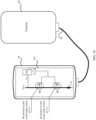
- a charger 30 is connected to an A mobile phone 10 through a universal serial bus (Universal Serial Bus, USB) 20.
- USB Universal Serial Bus
- the charger 30 is plugged into a socket, and the external power supply provides the external voltage V USB for the A mobile phone 10 by using the USB cable 20, the charging circuit 101 in the mobile phone receives the external voltage V USB .
- V USB 20 V
- the gate driver 1101 adjusts the drive voltage V G to 25 V based on the reference voltage V R of 20 V, and controls the gate-source voltages of both M1 and M2 to be 5 V by using V G , so that M1 and M2 are always in the on state under action of the gate-source voltages of 5 V.
- a current flows from a node corresponding to V USB to a node corresponding to the internal voltage V BUS , in other words, flows from the external power supply of the electronic device to the inside of the electronic device, so that forward charging is implemented, and the A mobile phone 10 displays "charging".
- M1 and M2 are in the on state when the gate-source voltages are greater than the threshold voltages.
- the gate-source voltages of both M1 and M2 keep stable at 5 V under control of V G , in other words, M1 and M2 are turned on and work stably under action of the gate-source voltages of 5 V.
- a B mobile phone 40 is connected to the A mobile phone 10 through the USB cable 20.
- a power supply inside the charging circuit 101 in the A mobile phone 10 provides the internal voltage V BUS .
- the gate driver 1101 adjusts the drive voltage V G to 25 V based on the reference voltage V R , and controls, by using V G , both M1 and M2 to be turned on under action of the gate-source voltages V GS of 5 V.
- a current flows from a node corresponding to the internal voltage V BUS to a node corresponding to the external voltage V USB .
- the external voltage V USB is input to the B mobile phone 40 through the USB cable 20, the B mobile phone 40 displays "charging", and reverse charging is implemented.
- M1 and M2 are in the on state when the gate-source voltages are greater than the threshold voltages.
- the gate-source voltages of both M1 and M2 keep stable at 5 V under control of V G , in other words, M1 and M2 are turned on and work stably under action of the gate-source voltages of 5 V.
- any charging circuit provided in this embodiment of this application is applicable to both a bidirectional charging scenario for wired charging and a bidirectional charging scenario for wireless charging, and this is not limited in this embodiment of this application.
- both M1 and M2 that are used are Si MOS transistors, and because on impedance of the Si MOS transistor is relatively large, heat is easily caused, and therefore, the electronic device is hot, safety during charging is relatively low, and efficiency of the charging circuit is also limited.
- the Si MOS transistor occupies a relatively large area, which is inconvenient for board layout.
- Bi-GaN HEMT Bidirectional gallium nitride high electron mobility transistor
- Si MOS transistors in the circuit shown in FIG. 1A may be replaced with a Bi-GaN HEMT, and bidirectional charging is implemented by using the Si MOS and the Bi-GaN HEMT, to reduce overall on impedance of the charging circuit and improve efficiency of the charging circuit.
- miniaturization of the Bi-GaN HEMT is more convenient for board layout.
- a drive voltage applicable to the Bi-GaN HEMT is relatively small, and when both the Si MOS transistor and the Bi-GaN HEMT work at a relatively small drive voltage V G (in other words, at same power), on impedance of the Si MOS transistor is relatively large, which still limits efficiency of the charging circuit.
- the charging circuit may be applied to an electronic device, to separately provide, for two switching transistors in the charging circuit, drive voltages adapted to the two switching transistors, to reduce respective on impedance of the two switching transistors, reduce on impedance of the charging circuit, and improve efficiency of the charging circuit.
- the charging circuit provided in embodiments of this application may be applied to electronic devices such as a mobile phone, a tablet computer, a desktop computer, a laptop computer, a notebook computer, an ultra-mobile personal computer (Ultra-mobile Personal Computer, UMPC), a handheld computer, a netbook, a personal digital assistant (Personal Digital Assistant, PDA), a wearable electronic device, and a smartwatch, to implement a bidirectional charging function for the electronic devices.
- electronic devices such as a mobile phone, a tablet computer, a desktop computer, a laptop computer, a notebook computer, an ultra-mobile personal computer (Ultra-mobile Personal Computer, UMPC), a handheld computer, a netbook, a personal digital assistant (Personal Digital Assistant, PDA), a wearable electronic device, and a smartwatch, to implement a bidirectional charging function for the electronic devices.
- electronic devices such as a mobile phone, a tablet computer, a desktop computer, a laptop computer, a notebook computer, an ultra-mobile personal computer (Ul
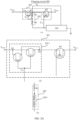
- an embodiment of this application discloses a charging circuit 200, including a switch circuit 201, a voltage divider circuit 202, and a gate driver 203.
- the switch circuit 201 is separately connected to the voltage divider circuit 202 and the gate driver 203.
- the switch circuit 201 includes a first switching transistor N1 and a second switching transistor N2.
- a first terminal D1 of the first switching transistor N1 is connected to an external device (namely, a device other than an electronic device in which the charging circuit 200 is located), and the first terminal D1 of the first switching transistor N1 receives, during forward charging, an external voltage V USB provided by the external device, and provides the external voltage V USB for the external device for charging during reverse charging.
- a second terminal D2 of the first switching transistor N1 is connected to a first terminal of the second switching transistor N2, and a control terminal of the first switching transistor N1 receives a first drive voltage V G1 output by the voltage divider circuit 202.
- the second terminal D2 of the first switching transistor N1 outputs a reference voltage V R .
- the first drive voltage V G1 is used to drive the first switching transistor N1 to be turned on or control N1 to be turned off.
- the reference voltage V R is a basis reference when the gate driver 203 adjusts a second drive voltage V G2 .
- the reference voltage V R is a voltage of the first terminal of the second switching transistor N2.
- the reference voltage V R is the voltage of the first terminal of the second switching transistor N2
- a difference between the second drive voltage and the reference voltage is equivalent to a value of a gate-source voltage of N2. Therefore, using the reference voltage as a reference to adjust the second drive voltage V G2 can control N2 to be turned on or turned off.
- a control terminal of the second switching transistor N2 is connected to the gate driver 203, and the control terminal of the second switching transistor N2 receives the second drive voltage V G2 output by the gate driver 203.
- a second terminal of the second switching transistor N2 is connected to the inside of the electronic device. The second terminal of the second switching transistor N2 outputs an internal voltage V BUS to an internal node of the electronic device during forward charging, to supply power to an internal component of the electronic device, and receives, during reverse charging, the internal voltage V BUS provided by an internal power supply of the electronic device.
- the second drive voltage V G2 is used to drive the second switching transistor N2 to be turned on or control N2 to be turned off.
- the internal voltage V BUS is a voltage of the internal node of the electronic device.
- the internal node of the electronic device is connected to the internal component of the electronic device.
- the internal component may be a power component, for example, a battery, or may be a component that needs to be powered, for example, a display screen or a speaker.
- the external voltage V USB is a voltage of an external node of the electronic device, and the external node is connected to the external device.
- the external device may be a power supply device, for example, a power supply, or may be a component that needs to be powered, for example, a power bank or an external keyboard.
- the first terminal of the first switching transistor N1 is an external node
- the second terminal of the second switching transistor N2 is an internal node.
- the first switching transistor N1 may be understood as a switching transistor, or may be understood as an equivalent switching transistor obtained after a plurality of switching transistors are connected in parallel.
- the second switching transistor N2 may also be understood as a switching transistor, or may be understood as an equivalent switching transistor obtained after a plurality of switching transistors are connected in parallel. That the plurality of switching transistors are connected in parallel means that gates of the plurality of switching transistors are connected, sources of the plurality of switching transistors are connected, and drains of the plurality of switching transistors are connected.
- a first switching transistor 2011 may be an equivalent switching transistor obtained after two switching transistors are connected in series. Specifically, first terminals of the two switching transistors are connected, and a common terminal between the first terminals of the two switching transistors is a D1 node, and may be equivalent to a first terminal of the first switching transistor 2011. Second terminals of the two switching transistors are connected, and a common terminal between the second terminals of the two switching transistors is a D2 node, and may be equivalent to a second terminal of the first switching transistor 2011. Control terminals of the two switching transistors are connected, and a common terminal between the second terminals of the two switching transistors may be equivalent to a control terminal of the first switching transistor 2011. The control terminal of the first switching transistor 2011 receives the first drive voltage V G1 .
- the first switching transistor N1 is a Bi-GaN HEMT, and due to a characteristic of the Bi-GaN HEMT, each of the first terminal D1 and the second terminal D2 of the first switching transistor N1 can be used as a source or a drain.
- the control terminal of the first switching transistor N2 may be a gate.
- the second switching transistor N2 is a Si MOS transistor.
- the first terminal of the second switching transistor N2 may be a source, the second terminal may be a drain, and the control terminal may be a gate.
- the voltage divider circuit 202 is separately connected to the switch circuit 201 and the gate driver 203.
- the voltage divider circuit 202 includes a first resistor R1 and a second resistor R2.
- a first terminal of the first resistor R1 receives the reference voltage V R . Therefore, a voltage of the first terminal of the first resistor R1 is the reference voltage V R .
- a second terminal of the first resistor R1 is connected to a first terminal of the second resistor R2, and a second terminal of the second resistor R2 receives the second drive voltage V G2 . Therefore, a voltage of the second terminal of the second resistor R2 is the second drive voltage V G2 .
- a common terminal between the first resistor R1 and the second resistor R2 outputs the first drive voltage V G1 .
- the other terminal of the second resistor R2 is connected to the gate driver 203, and the other terminal of the second resistor R2 receives the second drive voltage V G2 output by the gate driver 203.
- R1 may be understood as a resistor, or R1 may be understood as an equivalent resistor obtained after a plurality of resistors are connected in series and/or in parallel, and a resistance value of R1 is a resistance value of the equivalent resistor.
- R2 may also be understood as a resistor, or R2 may be understood as an equivalent resistor obtained after a plurality of resistors are connected in series and/or in parallel, and a resistance value of R2 is a resistance value of the equivalent resistor.
- the second resistor R2 may also be shown in 202 in FIG. 2A (3), to be specific, a second resistor 2021 may be an equivalent resistor obtained after two resistors are connected in series.
- the gate driver 203 is separately connected to the switch circuit 201 and the voltage divider circuit 202.
- the gate driver 203 is configured to: in a forward charging or reverse charging process, receive the reference voltage V R output by the switch circuit 201, and adjust a value of the second drive voltage V G2 to a first target drive voltage value based on the reference voltage V R , to control the second switching transistor N2 to be turned on.
- the second drive voltage V G2 is a drive voltage used to control N2 to be turned on or turned off.
- the first target drive voltage value is a value of the second drive voltage that can enable N2 to be in an on state.
- the first target drive voltage value may be a sum of the reference voltage V R and a first drive value.
- the first drive value is greater than a threshold voltage of the second switching transistor N2.
- the reference voltage is the voltage of the first terminal of the second switching transistor N2
- the second drive voltage is a voltage of the control terminal of the second switching transistor N2. Therefore, the value of the gate-source voltage of the second switching transistor N2 is the value of the second drive voltage V G2 minus a value of the reference voltage V R . Therefore, when the second drive voltage is adjusted to the first target drive voltage value, the value of the gate-source voltage of the second switching transistor N2 is equal to the first drive value. Because the first drive value is greater than the threshold voltage of the second switching transistor N2, N2 is in the on state.
- the first target drive voltage value may alternatively be a sum of N times of the reference voltage and the threshold voltage, where N is a positive integer greater than 1.
- N is a positive integer greater than 1.
- the gate driver 203 is further configured to: in a process of stopping forward charging or reverse charging, receive the reference voltage V R output by the switch circuit 201, and adjust the value of the second drive voltage V G2 to a second target drive voltage value based on the reference voltage V R , to control the second switching transistor N2 to be turned off.
- the second target drive voltage value is a value of the second drive voltage that can enable N2 to be in an off state.
- the second target drive voltage value may be a value of the reference voltage V R .
- the reference voltage is the voltage of the first terminal of the second switching transistor N2, and the second drive voltage is a voltage of the control terminal of the second switching transistor N2. Therefore, the value of the gate-source voltage of the second switching transistor N2 is the value of the second drive voltage V G2 minus the value of the reference voltage V R . Therefore, when the second drive voltage is adjusted to the second target drive voltage value, the value of the gate-source voltage of the second switching transistor N2 is equal to zero, and is less than the threshold voltage of the second switching transistor N2. Therefore, N2 is in the off state.
- the second target drive voltage value may alternatively be a negative value, and in this case, the value of the gate-source voltage of the second switching transistor N2 can also be less than the threshold voltage of the second switching transistor N2, so that N2 is turned off.
- the second target drive voltage value may alternatively be a negative value, and in this case, the value of the gate-source voltage of the second switching transistor N2 can also be less than the threshold voltage of the second switching transistor N2, so that N2 is turned off.
- the gate driver 203 is mainly used to adjust the second drive voltage by using the reference voltage as a reference and output the second drive voltage, to control the second switching transistor to be turned on or turned off, and a specific structure inside the gate driver 203 is not limited in this embodiment of this application.
- a specific working principle of the gate driver 203 refer to the foregoing descriptions of the related technical principle of the gate driver. Details are not described herein again.
- the gate driver 203 in the charging circuit 200 is configured to: receive the reference voltage V R , and adjust the value of the second drive voltage V G2 to the first target drive voltage value based on the reference voltage V R , to control the second switching transistor N2 to be turned on.
- the first target drive voltage value may be set to the sum of the reference voltage V R and the first drive value.
- the second switching transistor N2 is a Si MOS transistor, because on impedance is smaller when a gate-source voltage of the Si MOS transistor is larger, to improve efficiency of the charging circuit 200 and reduce on impedance of the circuit, a relatively large first drive value may be selected, so that the second switching transistor N2 is turned on under action of a relatively large gate-source voltage, thereby reducing the on impedance of N2.
- the first drive value may be set to 9 V.
- the gate driver 203 outputs the second drive voltage V G2 to the control terminal of the second switching transistor N2 in the switch circuit 201, so that N2 in the switch circuit 201 is turned on under control of the second drive voltage V G2 .
- the gate driver 203 further outputs the second drive voltage V G2 to the second terminal of the second resistor R2 in the voltage divider circuit 202.
- the first terminal of the first resistor in the voltage divider circuit 202 receives the reference voltage V R
- the second terminal of the second resistor R2 receives the second drive voltage V G2 . Therefore, the voltage of the first terminal of the first resistor is V R
- the second terminal of the second resistor R2 is V G2 .
- a voltage between the voltages of the second terminal of the second resistor R2 and the first terminal of the first resistor R1 is divided by using R1 and R2, to obtain the first drive voltage V G1 .
- the first drive voltage V G1 can control the first switching transistor N1 of the switch circuit 201 to be turned on or turned off.
- the value of the gate-source voltage of N1 is determined by the first drive value, the first resistor R1, and the second resistor R2. Because the first drive value is a fixed value, proper values of the first resistor R1 and the second resistor R2 may be selected, or a ratio of the first resistor R1 to the second resistor R2 may be adjusted, so that the gate-source voltage V1 of the first switching transistor N1 can be greater than a threshold voltage of N1, to drive N1 to be turned on.
- the values of the first resistor R1 and the second resistor R2 may be set based on an actual scenario requirement, a specific test situation, and the like.
- a process in which the first drive voltage V G1 controls the first switching transistor N1 of the switch circuit 201 to be turned on is as follows:
- an external power supply provides the external voltage V USB for the charging circuit 200
- a voltage of the first terminal D1 of N1 is the external voltage V USB
- N1 is initially in the off state.
- the second terminal D2 of N1 is a source of N1
- a voltage of the second terminal of N1 is the reference voltage V R .
- a voltage of the second terminal D2 of N1 is 0 V.
- the difference between the second drive voltage V G2 and the reference voltage V R is the first drive value, and is a fixed value. Therefore, the value of V1 is determined by R1 and R2.
- the value of the gate-source voltage V1 of N1 can be greater than the threshold voltage of N1, so that N1 is turned on. After N1 is turned on, N1 may be equivalent to a conducting wire.
- the value of the reference voltage V R is equivalent to the external voltage V USB .
- the second drive voltage is adjusted to increase by using the value of the reference voltage V R as a reference, so that the difference between the second drive voltage V G2 and the reference voltage V R is still the first drive value. Because the difference between the second drive voltage V G2 and the reference voltage V R remains unchanged, and the resistance values of the first resistor and the second resistor are also fixed, it can be learned from the foregoing calculation formula for V1 that V1 also remains unchanged, and is still greater than the threshold voltage, so that N1 continues to be turned on.
- the first switching transistor N1 when the first switching transistor N1 is a Bi-GaN HEMT, on impedance is relatively small at a relatively low gate-source voltage. For example, at a gate-source voltage of 5 V, the Bi-GaN HEMT is in the on state, and on impedance is relatively small. Therefore, when the first switching transistor N1 is a Bi-GaN HEMT, it can be learned from the foregoing descriptions of the calculation formula for V1 that proper R1 and R2 may be selected, so that the first switching transistor N1 works at the gate-source voltage of 5 V.
- the ratio of the resistance values of R1 and R2 is adjusted to 5:4, and V1 may be calculated as 5 V based on the foregoing calculation formula for the gate-source voltage V1 of N1, and therefore the first switching transistor N1 is turned on and works at the gate-source voltage of 5 V.
- the first terminal D1 of N1 of the switch circuit 201 receives the external voltage V USB
- the control terminal of N1 receives the first drive voltage V G1
- the control terminal of N2 receives the second drive voltage V G2
- the reference voltage V R is output to the gate driver 203 at the first terminal of N2.
- the first switching transistor N1 is turned on under control of the first drive voltage V G1
- the second switching transistor N2 is turned on under control of the second drive voltage V G2 .
- the switch circuit 201 outputs the internal voltage V BUS from the second terminal of the second switching transistor N2 based on the received external voltage V USB by using N1 and N2 that are turned on. In other words, a current inside the charging circuit 200 flows from the external voltage V USB to the internal voltage V BUS .
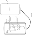
- the charging circuit 200 is applied to an A mobile phone 10.
- the external voltage V UBS is 20 V
- the ratio of the first resistor R1 to the second resistor R2 is 5:4
- the first switching transistor N1 is a Bi-GaN HEMT
- the second switching transistor N2 is a Si MOS transistor
- the charging circuit 200 can control the first switching transistor N1 to be turned on under action of a gate-source voltage of 5 V, and control the second switching transistor N2 to be turned on under action of a gate-source voltage of 9 V.
- the external device provides the external voltage V USB for the charging circuit 200, and the internal voltage V BUS is output by using N1 and N2 that are turned on.
- the external voltage V USB , the reference voltage V R , and the internal voltage V BUS are all 20 V.
- the gate driver 203 adjusts, for output, the second drive voltage V G2 to 29 V based on the reference voltage V R .
- the gate-source voltage of N2 is the second drive voltage V G2 minus the value of the reference voltage V R , and is equal to 9 V, and N2 is turned on and works under action of 9 V.
- V G2 29 V
- V R 20 V
- the ratio of the first resistor R1 to the second resistor R2 is 5:4
- N1 is turned on and works under action of 5 V.
- the charging circuit 200 may provide the internal voltage V BUS for the internal component of the electronic device, to charge the internal component of the electronic device, and the A mobile phone 10 is in a charging state. It should be noted that N1 and N2 are in the on state when the gate-source voltages are greater than the threshold voltages. In the scenario shown in FIG.
- the gate-source voltage of N1 is stable at 5 V
- the gate-source voltage of N2 is stable at 9 V
- N1 is turned on and works stably under action of the gate-source voltage of 5 V
- N2 is turned on and works stably under action of the gate-source voltage of 9 V.
- the first drive voltage V G1 controls the first switching transistor N1 to be turned on
- the second drive voltage V G2 controls the second switching transistor N2 to be turned on.
- Voltage values of the first drive voltage for controlling the first switching transistor N1 to be turned on and the second drive voltage for controlling the second switching transistor N2 to be turned on may be different.
- values of the gate-source voltage for driving the first switching transistor N1 to be turned on and the gate-source voltage for driving the second switching transistor N2 to be turned on may also be different.
- a first drive voltage V G1 that can enable the first switching transistor N1 to have smaller on impedance and lower power consumption may be selected, to control the first switching transistor N1 to be turned on
- a second drive voltage V G2 that can enable the second switching transistor N2 to have smaller on impedance and lower power consumption may be selected, to control the second switching transistor N2 to be turned on. Because both the first switching transistor N1 and the second switching transistor N2 are turned on under action of drive voltages adapted to the first switching transistor N1 and the second switching transistor N2, on impedance of the charging circuit is reduced, and forward charging efficiency of the charging circuit is improved.
- the charging circuit 200 When the electronic device to which the charging circuit 200 is applied is fully charged or the electronic device receives a charging stop instruction or the like, the charging circuit 200 needs to stop performing forward charging (in other words, perform forward turn-off). Specifically, referring to FIG. 2A (1), in a forward turn-off scenario, the gate driver 203 in the charging circuit 200 receives the reference voltage V R output by the switch circuit 201, and adjusts the value of the second drive voltage V G2 to the second target drive voltage value based on the reference voltage V R , to control the second switching transistor N2 to be turned off.
- the second target drive voltage value may be a value equal to the reference voltage V R .
- the second target drive voltage value refer to the foregoing related descriptions of the first target drive voltage value in the gate driver 203. Details are not described herein again.
- a process of turning off N2 is as follows: At an initial moment of the forward turn-off time period, N2 is still in the on state.
- the reference voltage V R is 20 V
- the gate driver 203 adjusts the second drive regulated voltage to a value equal to the reference voltage V R , and outputs the second drive voltage V G2 of 20 V, so that the gate-source voltage of the second switching transistor N2 is 0, and N2 is turned off.
- the reference voltage V R changes to 0 V
- the second drive voltage V G2 output by the gate driver 203 is adjusted to 0 V accordingly.
- V G2 decreases accordingly.
- V G2 is always equal to the value of V R , so that the gate-source voltage of N2 is always kept at 0, and the gate-source voltage of N2 is always less than the threshold voltage, and therefore N2 is always in the off state.
- the gate driver 203 outputs the second drive voltage V G2 to the control terminal of N2 in the switch circuit 201, so that after receiving the second drive voltage V G2 , the switch circuit 201 controls, under control of the second drive voltage V G2 , the second switching transistor N2 to be turned off.
- the gate driver 203 further outputs the second drive voltage V G2 to the second terminal of the second resistor R2 in the voltage divider circuit 202.
- the first terminal of the first resistor in the voltage divider circuit 202 receives the reference voltage V R
- the second terminal of the second resistor R2 receives the second drive voltage V G2 . Therefore, the voltage of the first terminal of the first resistor is V R , and the voltage of the second terminal of the second resistor R2 is V G2 .
- a voltage between the voltages of the second terminal of the second resistor R2 and the first terminal of the first resistor R1 is divided by using R1 and R2, to obtain the first drive voltage V G1 .
- the first drive voltage V G1 is a divided voltage between the reference voltage V R and the second drive voltage V G2
- a process in which the first drive voltage V G1 controls the first switching transistor N1 of the switch circuit 201 to be turned off is as follows: In the forward turn-off time period, a voltage of the control terminal of N1 is the first drive voltage, the second terminal D2 of N1 is a source of N1, a voltage of the second terminal of N1 is the reference voltage V R , and a voltage between the control terminal and the second terminal D2 of N1 is a gate-source voltage V1 of N1.
- the first drive voltage V G1 also controls N1 to be turned off.
- the first terminal D1 of N1 of the switch circuit 201 receives the external voltage V USB
- the control terminal of N1 receives the first drive voltage V G1
- the control terminal of N2 receives the second drive voltage V G2
- the reference voltage V R is output to the gate driver 203 at the first terminal of N2.
- the first switching transistor N1 is turned off under control of the first drive voltage V G1
- the second switching transistor N2 is turned off under control of the second drive voltage V G2 .
- the external voltage V USB cannot pass through N1 and N2 that are turned off to output a current, and therefore output of the internal voltage V BUS is stopped. In other words, the current inside the charging circuit 200 no longer flows from the external voltage V USB to the internal voltage V BUS .
- the charging circuit 200 repeatedly performs a process of performing forward charging and then performing forward turn-off.
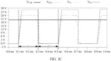
- a voltage change in the charging circuit 200 is shown in FIG. 2C .
- the gate driver 203 adjusts the second drive voltage V G2 to 29 V based on the reference voltage V R of 20 V.
- the first drive voltage V G1 is a divided voltage between the second drive voltage V G2 and the reference voltage V R , and is 25 V.
- the gate-source voltage of N1 is 5 V
- the gate-source voltage of N2 is 9 V
- both N1 and N2 are in the on state.
- the charging circuit 200 can output the internal voltage V BUS of 20 V by using N1 and N2 that are turned on. Taking a forward turn-off phase t2 as an example, the external voltage V USB is still 20 V, and in an initial phase of t2, N1 and N2 are not turned off, and the reference voltage is 20 V.
- the gate driver 203 adjusts the second drive voltage V G2 to be equal to the value of the reference voltage, so that N2 is turned off. After N2 is turned off, it can be learned from the foregoing calculation formula for the gate-source voltage of N1 that the gate-source voltage of N1 changes to 0 V, and N1 is turned off.
- the first drive voltage V G1 is a divided voltage between the second drive voltage V G2 and the reference voltage V R . Because both the second drive voltage and the reference voltage are 0 V, the first drive voltage V G1 is also 0 V, and N1 also continues to be in the off state. Because N1 and N2 are turned off, the current inside the charging circuit 200 no longer flows from the external voltage V USB to the internal voltage V BUS , and the internal voltage V BUS is 0.
- the gate driver 203 in the charging circuit 200 is configured to: receive the reference voltage V R , and adjust the value of the second drive voltage V G2 to the first target drive voltage value based on the reference voltage V R , to control the second switching transistor N2 to be turned on.
- the voltage divider circuit 202 divides the voltage between the second drive voltage V G2 and the reference voltage V R by using R1 and R2, to obtain the first drive voltage V G1 .
- the switch circuit 201 receives the internal voltage V BUS by using the second terminal of the second switching transistor N2, receives the first drive voltage V G1 by using the control terminal of the first switching transistor N1, receives the second drive voltage V G2 by using the control terminal of the second switching transistor N2, and outputs the reference voltage V R to the gate driver 203 by using the first terminal of N2.
- the first switching transistor N1 is turned on under control of the first drive voltage V G1
- the second switching transistor N2 is turned on under control of the second drive voltage V G2 .
- the switch circuit 201 receives the internal voltage V BUS by using the second terminal of the second switching transistor N2, and outputs the external voltage V USB from the first terminal D1 of N1 by using N1 and N2 that are turned on. In other words, a current inside the charging circuit 200 flows from the internal voltage V BUS to the external voltage V USB .
- the first drive voltage V G1 is not 0, and is greater than a threshold voltage of N1.
- a value of a gate-source voltage of N1 is equal to the value of the first drive voltage V G1 , and therefore N1 is turned on.
- a voltage value of the first terminal D1 of N1 a voltage value (namely, the reference voltage V R ) of the second terminal D2 of N1, and a value of the internal voltage V BUS are all equal.
- the reverse charging time period differs from the forward charging time period in that a current direction of the charging circuit 200 in the reverse charging time period is opposite to that in the forward charging time period, and is from the internal voltage V BUS to the external voltage V USB .
- the charging circuit 200 is applied to an A mobile phone 10.
- the internal voltage V BUS is 20 V
- the ratio of the first resistor R1 to the second resistor R2 is 5:4
- the first switching transistor N1 is a Bi-GaN HEMT
- the second switching transistor N2 is a Si MOS transistor
- the charging circuit 200 can control the first switching transistor N1 to be turned on under action of a gate-source voltage of 5 V
- N1 and N2 are in the on state when the gate-source voltages are greater than the threshold voltages.
- FIG. 1 the scenario shown in FIG.
- the gate-source voltage V1 of N1 is stable at 5 V under control of the first drive voltage V G1
- the gate-source voltage of N2 is stable at 9 V under control of the second drive voltage V G2
- N1 is turned on and works stably under action of the gate-source voltage of 5 V
- N2 is turned on and works stably under action of the gate-source voltage of 9 V.
- the electronic device when N1 and N2 are turned on and work stably, as shown by an arrow in FIG. 2D , the electronic device provides the internal voltage V BUS for the charging circuit 200, and outputs the external voltage V USB by using N1 and N2 that are turned on.
- the external voltage V USB , the reference voltage V R , and the internal voltage V BUS are all 20 V.
- the gate driver 203 adjusts, for output, the second drive voltage V G2 to the first target drive voltage value 29 V based on the reference voltage V R .
- the gate-source voltage of N2 is a value of the second drive voltage V G2 minus the reference voltage V R , and is equal to 9 V, and N2 is turned on and works under action of 9 V.
- V G2 29 V
- V R 20 V
- the ratio of the first resistor R1 to the second resistor R2 is 5:4
- the gate-source voltage of the first switching transistor N1 is a value of the first drive voltage V G1 minus the reference voltage V R , and is equal to 5 V.
- N1 and N2 are turned on.
- the current may flow from the internal voltage V BUS to the external voltage V USB , and a mobile phone 40 is charged by using the external voltage V USB .
- the first drive voltage V G1 controls the first switching transistor N1 to be turned on
- the second drive voltage V G2 controls the second switching transistor N2 to be turned on. Because the voltage for controlling the first switching transistor N1 to be turned on and the voltage for controlling the second switching transistor N2 to be turned on are different, the gate-source voltage for driving the first switching transistor N1 to be turned on and the gate-source voltage for driving the second switching transistor N2 to be turned on are also different.
- a first drive voltage V G1 that can enable the first switching transistor N1 to have smaller on impedance and lower power consumption may be selected, to control the first switching transistor N1 to be turned on
- a second drive voltage V G2 that can enable the second switching transistor N2 to have smaller on impedance and lower power consumption may be selected, to control the second switching transistor N2 to be turned on. Because both the first switching transistor N1 and the second switching transistor N2 are turned on under action of drive voltages adapted to the first switching transistor N1 and the second switching transistor N2, on impedance of the charging circuit is reduced, and reverse charging efficiency of the charging circuit is improved.
- the charging circuit 200 needs to stop performing reverse charging (in other words, perform reverse turn-off).
- the gate driver 203 in the charging circuit 200 receives the reference voltage V R output by the switch circuit 201, and adjusts the value of the second drive voltage V G2 to the second target drive voltage value based on the reference voltage V R , to control the second switching transistor N2 to be turned off.
- the gate driver 203 outputs the second drive voltage V G2 to the control terminal of N2 in the switch circuit 201, so that after receiving the second drive voltage V G2 , the switch circuit 201 controls, under control of the second drive voltage V G2 , the second switching transistor N2 to be turned off.
- the gate driver 203 further outputs the second drive voltage V G2 to the second terminal of the second resistor R2 in the voltage divider circuit 202.
- the first terminal of the first resistor in the voltage divider circuit 202 receives the reference voltage V R
- the second terminal of the second resistor R2 receives the second drive voltage V G2 . Therefore, the voltage of the first terminal of the first resistor is V R
- the voltage of the second terminal of the second resistor R2 is V G2 .
- a voltage between the voltages of the second terminal of the second resistor R2 and the first terminal of the first resistor R1 is divided by using R1 and R2, to obtain the first drive voltage V G1 .
- the first drive voltage V G1 is a divided voltage between the reference voltage V R and the second drive voltage V G2 .
- the gate driver 203 adjusts the value of the second drive voltage to be equal to the reference voltage V R , it can be ensured that the gate-source voltage of N2 is 0. Because the gate-source voltage of N2 is less than the threshold voltage, N2 can remain in the off state. After N2 is turned off, the reference voltage V R falls to 0, and the gate driver 203 correspondingly adjusts the second drive voltage V G2 to 0 V.
- the first drive voltage V G1 is a divided voltage between the reference voltage V R and the second drive voltage V G2 . Therefore, the first drive voltage also falls to 0 V, and therefore the first switching transistor N1 is also turned off.
- the first terminal D1 of N1 of the switch circuit 201 receives the internal voltage V BUS
- the control terminal of N1 receives the first drive voltage V G1
- the control terminal of N2 receives the second drive voltage V G2
- the reference voltage V R is output to the gate driver 203 at the first terminal of N2.
- the first switching transistor N1 is turned off under control of the first drive voltage V G1
- the second switching transistor N2 is turned off under control of the second drive voltage V G2 .
- the internal voltage V BUS cannot pass through N1 and N2 that are turned off to output the external voltage V USB . In other words, a current inside the charging circuit 200 no longer flows from the internal voltage V BUS to the external voltage V USB .
- the charging circuit 200 repeatedly performs a process of performing reverse charging and then performing reverse turn-off.
- a voltage change in the charging circuit 200 is shown in FIG. 2E .
- the gate driver 203 adjusts the second drive voltage V G2 to 29 V based on the reference voltage V R of 20 V.
- the first drive voltage V G1 is a divided voltage between the reference voltage V R and the second drive voltage V G2 , and is 25 V.
- a gate-source voltage is 5 V
- the gate-source voltage of N2 is 9 V
- both N1 and N2 are in the on state.
- the charging circuit 200 can output the output voltage V USB of 20 V by using N1 and N2 that are turned on.
- N1 and N2 are not turned off, and the reference voltage is 20 V.
- the gate driver 203 adjusts the second drive voltage V G2 to be equal to a value of the reference voltage, so that N2 is turned off. After N2 is turned off, the reference voltage falls to 0 V, and the second drive voltage V G2 falls to 0 V accordingly, so that N2 continues to be turned off.
- the first drive voltage V G1 is a divided voltage between the reference voltage V R and the second drive voltage V G2 . Because both the second drive voltage and the reference voltage are 0 V, the first drive voltage V G1 is also 0 V, and further, N1 is turned off. Because N1 and N2 are turned off, the current inside the charging circuit 200 no longer flows from the internal voltage V BUS to the external voltage V USB , and the external voltage V USB is 0.
- an embodiment of this application discloses another charging circuit 300, including a switch circuit 301, a voltage divider circuit 302, and a gate driver 303.
- a structure and an operating principle of the gate driver 303 are the same as those of the gate driver 203 in FIG. 2A
- a structure and an operating principle of the voltage divider circuit 302 are the same as those of the voltage divider circuit 202 in FIG. 2A
- a structure and an operating principle of the switch circuit 301 are different from those of the switch circuit 201 in FIG. 2A .
- a structure of the charging circuit 300 in FIG. 3A is as follows:
- the switch circuit 301 is separately connected to the voltage divider circuit 302 and the gate driver 303, and the switch circuit 303 includes a first switching transistor N1, a second switching transistor N2, and a third resistor R3.
- a first terminal D1 of the first switching transistor N1 is connected to an external device (namely, a device other than an electronic device in which the charging circuit 300 is located), and the first terminal D1 of the first switching transistor N1 receives, during forward charging, an external voltage V USB provided by the external device, and provides the external voltage V USB for the external device for charging during reverse charging.
- a second terminal D2 of the first switching transistor N1 is connected to a second terminal of the second switching transistor N2.
- a control terminal of the first switching transistor N1 receives a first drive voltage V G1 .
- the first drive voltage V G1 is used to drive the first switching transistor N1 to be turned on or control N1 to be turned off.
- a reference voltage V R is a basis reference when the gate driver 303 adjusts a second drive voltage V G2 .
- the reference voltage V R is a voltage of a first terminal of the second switching transistor N2.
- the reference voltage V R is the voltage of the first terminal of the second switching transistor N2.
- a difference between the second drive voltage and the reference voltage is equivalent to a value of a gate-source voltage of N2. Therefore, using the reference voltage as a reference to adjust the second drive voltage V G2 can control N2 to be turned on or turned off.
- the second terminal D2 of the first switching transistor N1 outputs an internal voltage V BUS during forward charging, and receives, during reverse charging, the internal voltage V BUS provided by an internal power supply of the electronic device.
- the internal voltage V BUS is a voltage of an internal node of the electronic device, and the internal node of the electronic device may be connected to an internal component of the electronic device.
- the internal component may be a power component, for example, a battery, or may be a component that needs to be powered, for example, a display screen or a speaker.
- the external voltage V USB is a voltage of an external node of the electronic device, and the external node is connected to the external device.
- the external device may be a power supply device, for example, a power supply, or may be a component that needs to be powered, for example, a power bank or an external keyboard.
- the external node is the first terminal D1 of the first switching transistor N1
- the internal node is the second terminal D2 of the first switching transistor N1.
- a control terminal of the second switching transistor N2 receives the second drive voltage V G2 , and the first terminal of the second switching transistor N2 is grounded by using the third resistor R3.
- the first terminal of the second switching transistor N2 outputs the reference voltage V R .
- the second drive voltage V G2 is used to drive the second switching transistor N2 to be turned on or control N2 to be turned off.
- the first switching transistor N1 may be understood as a switching transistor, or may be understood as an equivalent switching transistor obtained after a plurality of switching transistors are connected in parallel.
- the second switching transistor N2 may also be understood as a switching transistor, or may be understood as an equivalent switching transistor obtained after a plurality of switching transistors are connected in parallel. That the plurality of switching transistors are connected in parallel means that gates of the plurality of switching transistors are connected, sources of the plurality of switching transistors are connected, and drains of the plurality of switching transistors are connected. Specifically, for a parallel structure between the plurality of switching transistors, refer to 2011 shown in FIG. 2A (2).
- the first switching transistor N1 is a Bi-GaN HEMT, and due to a characteristic of the Bi-GaN HEMT, each of the first terminal D1 and the second terminal D2 of the first switching transistor N1 can be used as a source or a drain.
- the control terminal of the first switching transistor N2 may be a gate.
- the second switching transistor N2 is a Si MOS transistor.
- the first terminal of the second switching transistor N2 may be a source, the second terminal may be a drain, and the control terminal may be a gate.
- the voltage divider circuit 302 is separately connected to the gate driver 303 and the switch circuit 301, and the voltage divider circuit 302 includes a first resistor R1 and a second resistor R2.
- a first terminal of the first resistor R1 receives the reference voltage V R
- a second terminal of the first resistor R1 is connected to a first terminal of the second resistor R2
- a second terminal of the second resistor R2 receives the second drive voltage V G2 .
- a common terminal between the first resistor R1 and the second resistor R2 outputs the first drive voltage V G1 .
- R1 may be understood as a resistor, or R1 may be understood as an equivalent resistor obtained after a plurality of resistors are connected in series and/or in parallel, and a resistance value of R1 is a resistance value of the equivalent resistor.
- R2 may also be understood as a resistor, or R2 may be understood as an equivalent resistor obtained after a plurality of resistors are connected in series and/or in parallel, and a resistance value of R2 is a resistance value of the equivalent resistor.
- the second resistor R2 may also be shown in 202 in FIG. 2A (3), to be specific, a second resistor 2021 may be an equivalent resistor obtained after two resistors are connected in series.
- composition, a structure, and a working principle of the voltage divider circuit 302 refer to the voltage divider circuit 202 shown in FIG. 2A .
- the gate driver 303 is separately connected to the switch circuit 301 and the voltage divider circuit 302.
- the gate driver 303 is configured to: in a forward charging or reverse charging process, receive the reference voltage V R output by the switch circuit 301, and adjust a value of the second drive voltage V G2 to a first target drive voltage value based on the reference voltage V R , to control the second switching transistor N2 to be turned on.
- the second drive voltage V G2 is a drive voltage used to control N2 to be turned on or turned off.
- the first target drive voltage value is a value of the second drive voltage that can enable N2 to be in an on state.
- the gate driver 303 is further configured to: in a process of stopping forward charging or reverse charging, receive the reference voltage V R output by the switch circuit 301, and adjust the value of the second drive voltage V G2 to a second target drive voltage value based on the reference voltage V R , to control the second switching transistor N2 to be turned off.
- the second target drive voltage value is a value of the second drive voltage that can enable N2 to be in an off state.
- composition and a connection structure of the gate driver 303 refer to the gate driver 203 shown in FIG. 2A .
- the gate driver 303 in the charging circuit 300 is configured to: receive the reference voltage V R , and adjust the value of the second drive voltage V G2 to the first target drive voltage value based on the reference voltage V R , to control the second switching transistor N2 to be turned on.
- the first terminal of the first resistor R1 in the voltage divider circuit 302 receives the reference voltage V R
- the control terminal of the second switching transistor N2 receive the second drive voltage V G2
- the voltage between the reference voltage V R and the second drive voltage V G2 is divided by using R1 and R2, to obtain the first drive voltage V G1 .
- the first drive voltage V G1 is a divided voltage between the reference voltage V R and the second drive voltage V G2
- the first drive voltage V G1 can control the first switching transistor N1 of the switch circuit 301 to be turned on or turned off.
- the switch circuit 301 receives the external voltage V USB by using the first terminal of N1, receives the first drive voltage V G1 by using the control terminal of N1, receives the second drive voltage V G2 by using the control terminal of N2, and outputs the reference voltage V R to the gate driver 303 by using a common terminal between the first terminal of the second switching transistor N2 and the third resistor.
- the first switching transistor N1 is turned on under control of the first drive voltage V G1
- the second switching transistor N2 is turned on under control of the second drive voltage V G2 .
- the external voltage V USB passes through N1 that is turned on to obtain and output the internal voltage V BUS .
- a current inside the charging circuit 200 flows from the external voltage V USB to the internal voltage V BUS .
- the value of the second drive voltage V G2 output by the gate driver 303 is adjusted based on the reference voltage V R , the value (namely, the difference between the second drive voltage and the reference voltage V R ) of the gate-source voltage applied to N2 can always be greater than a threshold voltage of N2, so that N2 is in the on state.
- the gate driver 303 For a specific process and principle of controlling the second switching transistor N2 to be turned on by the gate driver 303, refer to the foregoing process and principle of controlling N2 to be turned on by the gate driver 202 in FIG. 2A . Details are not described herein again.
- the first target drive voltage value may be a sum of the reference voltage V R and a first drive value
- a process of turning on N1 in the forward charging scenario is as follows:
- the second terminal D2 of N1 is a source of N1
- a voltage of the second terminal D2 of N1 at an initial moment is 0,
- a value of a gate-source voltage (namely, a voltage between the control terminal of N1 and the second terminal D2 of N1) of N1 is equivalent to the value of the first drive voltage V G1
- the value of the first drive voltage V G1 may be greater than a threshold voltage of N1, so that N1 is turned on.
- a voltage of the second terminal D2 of N1 is equal to a value of the external voltage V USB .
- the gate driver correspondingly adjusts the second drive voltage V G2 .
- the charging circuit 300 is applied to an A mobile phone 10.
- the external voltage V UBS is 20 V
- a ratio of the first resistor R1 to the second resistor R2 is 5:4
- the first switching transistor N1 is a Bi-GaN HEMT
- the second switching transistor N2 is a Si MOS transistor
- the charging circuit 300 can control the first switching transistor N1 to be turned on under action of a gate-source voltage of 5 V
- N1 and N2 are in the on state when the gate-source voltages are greater than the threshold voltages.
- FIG. 1 the scenario shown in FIG.
- the gate-source voltage of N1 is stable at 5 V
- the gate-source voltage of N2 is stable at 9 V
- N1 is turned on and works stably under action of the gate-source voltage of 5 V
- N2 is turned on and works stably under action of the gate-source voltage of 9 V.
- an external power supply provides the external voltage V USB for the charging circuit 300, and the internal voltage V BUS is output by using N1 that is turned on.
- both the external voltage V USB and the internal voltage V BUS are 20 V.
- the reference voltage V R is also 20 V.
- the gate driver 303 adjusts the second drive voltage V G2 to 29 V based on the reference voltage V R . Therefore, the gate-source voltage of N2 is 9 V, and N2 is turned on and works under action of 9 V.
- the second drive voltage V G2 is 29 V
- V R is 20 V
- the ratio of the first resistor R1 to the second resistor R2 is 5:4
- N1 is turned on and works under action of 5 V.
- the charging circuit 300 may provide the internal voltage V BUS for the inside of the electronic device, to charge the inside of the electronic device, and the A mobile phone 10 is in a charging state.
- the first drive voltage V G1 controls the first switching transistor N1 to be turned on
- the second drive voltage V G2 controls the second switching transistor N2 to be turned on. Because the voltage for controlling the first switching transistor N1 to be turned on and the voltage for controlling the second switching transistor N2 to be turned on may be different, a value of the gate-source voltage for driving the first switching transistor N1 to be turned on and a value of the gate-source voltage for driving the second switching transistor N2 to be turned on may also be different.
- a first drive voltage V G1 that can enable the first switching transistor N1 to have smaller on impedance and lower power consumption may be selected, to control the first switching transistor N1 to be turned on
- a second drive voltage V G2 that can enable the second switching transistor N2 to have smaller on impedance and lower power consumption may be selected, to control the second switching transistor N2 to be turned on. Because both the first switching transistor N1 and the second switching transistor N2 are turned on under action of drive voltages adapted to the first switching transistor N1 and the second switching transistor N2, on impedance of the charging circuit is reduced, and forward charging efficiency of the charging circuit is improved.
- the charging circuit 300 mainly differs in that the external voltage V USB is transmitted to a branch of the internal voltage V BUS that implements a forward charging action, and the current passes through only the first switching transistor N1. Because the branch passes through only one switching transistor, compared with the charging circuit 200, during forward charging, on impedance of the branch is smaller, forward charging efficiency is higher, and power consumption is lower.
- the charging circuit 300 When the electronic device to which the charging circuit 300 is applied is fully charged or the electronic device receives a charging stop instruction or the like, the charging circuit 300 needs to stop performing forward charging. Specifically, referring to FIG. 3A , in a forward turn-off scenario, the gate driver 303 in the charging circuit 300 receives the reference voltage V R output by the switch circuit 301, and adjusts the value of the second drive voltage VG2 to the second target drive voltage value based on the reference voltage V R , to control the second switching transistor N2 to be turned off.
- the voltage divider circuit 302 receives the reference voltage V R by using the first terminal of the first resistor R1, receives the second drive voltage V G2 by using the second terminal of the second resistor R2, and then divides the voltage between the reference voltage V R and the second drive voltage V G2 by using R1 and R2, to obtain the first drive voltage V G1 .
- the first drive voltage V G1 can control the first switching transistor N1 of the switch circuit 301 to be turned off.
- the switch circuit 301 receives the external voltage V USB by using the first terminal D1 of N1, receives the first drive voltage V G1 by using the control terminal of N1, receives the second drive voltage V G2 by using the control terminal of N2, and outputs the reference voltage V R to the gate driver 303 by using a common terminal between the first terminal of the second switching transistor N2 and the third resistor.
- the second switching transistor N2 is turned off under control of the second drive voltage V G2
- the first switching transistor N1 is also turned off under control of the first drive voltage V G1 .
- the first switching transistor N1 is turned off, the external voltage V USB cannot pass through N1 to output a current, and therefore output of the internal voltage V BUS is stopped. In other words, the current inside the charging circuit 200 no longer flows from the external voltage V USB to the internal voltage V BUS through N1.
- the gate driver 303 adjusts, in the forward turn-off scenario, the second drive voltage V G2 to be equal to the reference voltage V R , the gate-source voltage of N2 is 0, and N2 may be controlled to be in the off state.
- the first terminal of N2 is grounded, and the reference voltage V R falls to 0 V. Therefore, the second drive voltage V G2 also decreases with the reference voltage V R , and also falls to 0 V.
- the first drive voltage V G1 is a divided voltage between the second drive voltage V G2 and the reference voltage V R .
- the first drive voltage V G1 is also 0 V, and the first switching transistor N1 is turned off under control of the first drive voltage V G1 of 0 V. Therefore, in the forward turn-off scenario, N2 is controlled, by using the second drive voltage, to be turned off, so that the first drive voltage can control N1 to be turned off.
- the charging circuit 300 repeatedly performs a process of performing forward charging and then performing forward turn-off.
- a voltage change in the charging circuit 300 is shown in FIG. 3C .
- the external voltage V USB provided by an external power supply for the charging circuit 300 is 20 V
- the gate driver 303 adjusts the second drive voltage V G2 to 29 V based on the reference voltage V R .
- the first drive voltage V G1 is a divided voltage between the second drive voltage V G2 and the reference voltage V R , and a ratio of the first resistor R1 to the second resistor R2 is 5:4. Therefore, the first drive voltage is 25 V.
- both N1 and N2 are in the on state, so that the external voltage V USB can pass through N1 that is turned on to output the internal voltage V BUS of 20 V.
- the external voltage V USB received by the charging circuit 200 is 20 V
- the second drive voltage V G2 falls to 0 V along with the reference voltage V R in the forward turn-off scenario, so that N1 is turned off.
- the first drive voltage is a divided voltage between the second drive voltage and the reference voltage
- the first drive voltage also changes to 0 V, so that N1 is also turned off. Because N1 and N2 are turned off, the current inside the charging circuit 200 no longer flows from the external voltage V USB to the internal voltage V BUS , and the internal voltage V BUS is 0.
- the gate driver 303 in the charging circuit 300 is configured to: receive the reference voltage V R , and adjust the value of the second drive voltage V G2 to the first target drive voltage value based on the reference voltage V R , to control the second switching transistor N2 to be turned on.
- the voltage divider circuit 302 receives the reference voltage V R by using the first terminal of the first resistor R1, receives the second drive voltage V G2 by using the second terminal of the second resistor R2, and divides the voltage difference between the reference voltage V R and the second drive voltage V G2 by using R1 and R2, to obtain the first drive voltage V G1 .
- the switch circuit 301 receives the internal voltage V BUS by using the second terminal of the first switching transistor N1, receives the first drive voltage V G1 by using the control terminal of N1, receives the second drive voltage V G2 by using the control terminal of N2, and outputs the reference voltage V R to the gate driver 303 by using the first terminal of N2.
- the first switching transistor N1 is turned on under control of the first drive voltage V G1
- the second switching transistor N2 is turned on under control of the second drive voltage V G2 .
- the internal voltage V BUS received by the second terminal of N1 passes through N1 that is turned on to output the external voltage V USB from the second terminal of N1.
- a current inside the charging circuit 300 flows from the internal voltage V BUS to the external voltage V USB .
- the reference voltage is equal to the internal voltage V BUS provided by the inside of the electronic device, and the difference between the second drive voltage and the reference voltage is a first drive value, and is a fixed value
- the first drive voltage V G1 is greater than a threshold voltage of N1, so that N1 can be turned on.
- a working process and a principle in the reverse charging scenario are similar to those during forward charging, and a main difference is that a current direction is opposite to that in the forward charging scenario, and is from the internal voltage V BUS to the external voltage V USB .
- a current direction is opposite to that in the forward charging scenario, and is from the internal voltage V BUS to the external voltage V USB .
- the charging circuit 300 is applied to an A mobile phone 10.
- the internal voltage V BUS is 20 V
- a ratio of the first resistor R1 to the second resistor R2 is 5:4
- the first switching transistor N1 is a Bi-GaN HEMT
- the second switching transistor N2 is a Si MOS transistor
- the charging circuit 300 can control the first switching transistor N1 to be turned on under action of a gate-source voltage of 5 V
- N1 and N2 are in the on state when the gate-source voltages are greater than threshold voltages.
- FIG. 1 the scenario shown in FIG.
- the gate-source voltage of N1 is stable at 5 V
- the gate-source voltage of N2 is stable at 9 V
- N1 is turned on and works stably under action of the gate-source voltage of 5 V
- N2 is turned on and works stably under action of the gate-source voltage of 9 V.
- an internal power supply of the electronic device provides the internal voltage V BUS for the charging circuit 300, and outputs the external voltage V USB by using N1 that is turned on.
- the external voltage V USB , the reference voltage V R , and the internal voltage V BUS are all 20 V.
- the gate driver 303 adjusts the second drive voltage V G2 to the first target drive voltage value 29 V based on the reference voltage V R , and therefore, the gate-source voltage of N2 is 9V, and N2 is turned on and works under action of 9 V.
- V G2 29 V
- V R 20 V
- the ratio of the first resistor R1 to the second resistor R2 5:4
- the first drive voltage V G1 controls the first switching transistor N1 to be turned on
- the second drive voltage V G2 controls the second switching transistor N2 to be turned on. Because the voltage for controlling the first switching transistor N1 to be turned on and the voltage for controlling the second switching transistor N2 to be turned on may be different, a value of the gate-source voltage for driving the first switching transistor N1 to be turned on and a value of the gate-source voltage for driving the second switching transistor N2 to be turned on may also be different.
- a first drive voltage V G1 that can enable the first switching transistor N1 to have smaller on impedance and lower power consumption may be selected, to control the first switching transistor N1 to be turned on
- a second drive voltage V G2 that can enable the second switching transistor N2 to have smaller on impedance and lower power consumption may be selected, to control the second switching transistor N2 to be turned on. Because both the first switching transistor N1 and the second switching transistor N2 are turned on under action of drive voltages adapted to the first switching transistor N1 and the second switching transistor N2, on impedance of the charging circuit is reduced, and reverse charging efficiency of the charging circuit is improved.
- the charging circuit 300 mainly differs in that the internal voltage V BUS is transmitted to a branch of the external voltage V USB that implements a reverse charging action, and the current passes through only the first switching transistor N1. Because the branch passes through only one switching transistor, compared with the charging circuit 200, during reverse charging, on impedance of the branch is smaller, reverse charging efficiency is higher, and power consumption is lower.
- the charging circuit 300 needs to stop performing reverse charging (in other words, perform reverse turn-off).
- the gate driver 303 in the charging circuit 300 receives the reference voltage V R output by the switch circuit 301, and adjusts the value of the second drive voltage V G2 to the second target drive voltage value based on the reference voltage V R , to control the second switching transistor N2 to be turned off.
- the second drive voltage V G2 output by the gate driver 303 is output to the switch circuit 301, so that after receiving the second drive voltage V G2 , the switch circuit 301 controls, under control of the second drive voltage V G2 , the second switching transistor N2 to be turned off.
- the second drive voltage V G2 output by the gate driver 303 is further received by the second terminal of the second resistor of the voltage divider circuit 302.
- the voltage divider circuit 302 receives the reference voltage V R by using the first terminal of the first resistor R1, receives the second drive voltage V G2 by using the second terminal of the second resistor R2, and divides the voltage difference between the reference voltage V R and the second drive voltage V G2 by using R1 and R2, to obtain the first drive voltage V G1 .
- the first drive voltage V G1 can control the first switching transistor N1 of the switch circuit 201 to be turned off.
- the switch circuit 301 receives the internal voltage V BUS by using the second terminal D2 of N1, receives the first drive voltage V G1 by using the control terminal of N1, receives the second drive voltage V G2 by using the control terminal of N2, and outputs the reference voltage V R by using a common terminal between the first terminal of the second switching transistor N2 and the third resistor.
- the first switching transistor N1 is turned off under control of the first drive voltage V G1
- the second switching transistor N2 is turned off under control of the second drive voltage V G2 .
- the internal voltage V BUS cannot pass through N1 to obtain and output the external voltage V USB . In other words, a current inside the charging circuit 300 no longer flows from the internal voltage V BUS to the external voltage V USB .
- the charging circuit 300 repeatedly performs a process of performing reverse charging and then performing reverse turn-off.
- a voltage change in the charging circuit 300 is shown in FIG. 3E .
- the internal voltage V BUS received by the charging circuit 300 is 20 V
- the gate driver 303 adjusts the second drive voltage V G2 to 29 V based on the reference voltage V R .
- the first drive voltage V G1 is a divided voltage between the reference voltage V R and the second drive voltage V G2 , and is 25 V.
- both N1 and N2 are in the on state, and therefore the internal voltage V BUS can pass through N1 that is turned on to output the external voltage V USB of 20 V.
- the internal voltage V BUS received by the charging circuit 300 is 20 V
- the second drive voltage V G2 falls to 0 V along with the reference voltage V R in a scenario in which reverse charging is stopped, so that N2 is turned off.
- the first drive voltage V G1 is a divided voltage between the second drive voltage V G2 and the reference voltage V R . Because both the second drive voltage V G2 and the reference voltage V R fall to 0 V, the first drive voltage V G1 also changes to 0 V, so that N1 is turned off. Because N1 is turned off, the current inside the charging circuit 300 no longer flows from the internal voltage V BUS to the external voltage V USB , and the external voltage V USB is 0.
- the switch circuit can output the reference voltage to the gate driver in the forward charging time period, the reverse charging time period, the forward turn-off time period, or the reverse turn-off time period, and in the forward charging time period or the reverse charging time period, the switch circuit can control, by using the first drive voltage, the first switching transistor to be turned on, and control, by using the second drive voltage, the second switching transistor to be turned on.
- both the first switching transistor N1 and the second switching transistor N2 are turned on, by using the first drive voltage and the second drive voltage that are different, under action of gate-source voltages suitable for the first switching transistor N1 and the second switching transistor N2, so that on impedance of the charging circuit is reduced, and bidirectional charging efficiency of the charging circuit is improved.
- the switch circuit may further control, by using the first drive voltage, the first switching transistor to be turned off, and control, by using the second drive voltage, the second switching transistor to be turned off.
- N1 and N2 are turned off, forward charging or reverse charging may be stopped.
- the switch circuit in FIG. 2A receives the external voltage, and outputs the internal voltage to the inside of the electronic device by using the first switching transistor and the second switching transistor that are turned on, in the reverse charging time period, the switch circuit receives the internal voltage, and outputs the external voltage to the outside of the electronic device by using the first switching transistor and the second switching transistor that are turned on, in the forward turn-off time period, the switch circuit receives the external voltage, and stops outputting the internal voltage to the inside of the electronic device by using the first switching transistor and the second switching transistor that are turned off, and in the reverse turn-off time period, the switch circuit receives the internal voltage, and stops outputting the external voltage to the outside of the electronic device by using the first switching transistor and the second switching transistor that are turned off.
- the first switching transistor and the second switching transistor that are turned on need to be used to implement charging
- the first switching transistor and the second switching transistor that are turned off need to be used to implement turn-off.
- the switch circuit in FIG. 3A receives the external voltage, and outputs the internal voltage to the inside of the electronic device by using the first switching transistor that is turned on, in the reverse charging time period, the switch circuit receives the internal voltage, and outputs the external voltage to the outside of the electronic device by using the first switching transistor that is turned on, in the forward turn-off time period, the switch circuit receives the external voltage, and stops outputting the internal voltage to the inside of the electronic device by using the first switching transistor that is turned off, and in the reverse turn-off time period, the switch circuit receives the internal voltage, and stops outputting the external voltage to the outside of the electronic device by using the first switching transistor that is turned off.
- the voltage divider circuits in FIG. 2A and FIG. 3A are configured to perform voltage division by using the reference voltage and the second drive voltage, to obtain and output the first drive voltage. It can be learned from FIG. 2A and FIG. 3A that the gate drivers in FIG. 2A and FIG.
- 3A adjust and output the second drive voltage based on the reference voltage in the forward charging time period or the reverse charging time period, and also adjust and output the second drive voltage based on the reference voltage in the forward turn-off time period or the reverse turn-off time period.
- specific manners of adjusting the second drive voltage in the charging time period and the turn-off time period are different. Specifically, in the forward charging time period or the reverse charging time period, the value of the second drive voltage is adjusted to the sum of the reference voltage and the first drive value, and the second drive voltage is output, but in the forward turn-off time period or the reverse turn-off time period, the value of the second drive voltage is adjusted to the value of the reference voltage, and the second drive voltage is output.
- the switch circuit is configured to: receive a power supply voltage and a plurality of drive voltages, and output a reference voltage and an output voltage of the charging circuit.
- the plurality of drive voltages include a first drive voltage and a second drive voltage.
- the voltage divider circuit is configured to: receive the second drive voltage and the reference voltage, and output the first drive voltage.
- the gate driver is configured to: receive the reference voltage, and output the second drive voltage.
- the power supply voltage is a voltage supplying power to the charging circuit.
- the output voltage of the charging circuit is a voltage provided by the charging circuit for a component that needs to be powered.
- the power supply voltage may be the external voltage mentioned in FIG. 2A and FIG. 3A in a forward charging time period, and may be an internal voltage in a reverse charging time period.
- the output voltage of the charging circuit is the internal voltage in the forward charging time period, and is the external voltage in the reverse charging time period.
- the external voltage is a voltage of an external node in the charging circuit, and the internal voltage is a voltage of an internal node in the charging circuit.
- the power supply voltage is the external voltage in a forward turn-off time period, and is the internal voltage in a reverse turn-off time period.
- the output voltage of the charging circuit is the internal voltage in the forward turn-off time period, and is the external voltage in the reverse turn-off time period.
- the switch circuit can obtain the first drive voltage and the second drive voltage by using the gate driver and the voltage divider circuit, and voltage values of the first drive voltage and the second drive voltage may be different. Therefore, the switch circuit may use a proper first drive voltage and a proper second drive voltage, to reduce on impedance of the charging circuit and improve bidirectional charging efficiency of the charging circuit.
- an embodiment of this application further discloses a charging system.
- the charging system includes at least a first electronic device, the first electronic device includes a charging management module, and the charging management module includes any one of the charging circuits provided in the foregoing embodiments of this application.
- the charging system further includes a charger connected to the first electronic device and/or a second electronic device connected to the first electronic device.
- the charger connected to the first electronic device is configured to output a power supply voltage to the first electronic device
- the second electronic device connected to the first electronic device is configured to receive an output voltage of the charging circuit.
- an embodiment of this application further discloses an electronic device 400.
- the electronic device 400 may be a tablet computer, a desktop computer, a laptop computer, a notebook computer, an ultra-mobile personal computer (Ultra-mobile Personal Computer, UMPC), a handheld computer, a netbook, a personal digital assistant (Personal Digital Assistant, PDA), a wearable electronic device, or the like.
- the electronic device 400 includes a processor 401, a charging management module 402, a power management module 403, and a USB interface 404.
- the charging management module 402 includes a charging circuit 4021.
- the structure illustrated in this embodiment does not constitute a specific limitation on the electronic device 400.
- the electronic device 400 may include more or fewer components than those shown in the figure, or may combine some components, or may split some components, or may have different component arrangements.
- the components shown in the figure may be implemented by using hardware, software, or a combination of software and hardware.
- the processor 401 may include one or more processing units.
- the processor 110 may include an application processor (application processor, AP), a modem processor, a graphics processing unit (graphics processing unit, GPU), an image signal processor (image signal processor, ISP), a controller, a video codec, a digital signal processor (digital signal processor, DSP), a baseband processor, and/or a neural-network processing unit (neural-network processing unit, NPU).
- Different processing units may be independent components, or may be integrated into one or more processors.
- the processor 401 may control the charging circuit 4021 to perform forward charging, reverse charging, stop forward charging, or stop reverse charging.
- the charging management module 402 is configured to: receive, from the charger, an external voltage V USB input through charging, or provide an external voltage V USB to the outside.
- the charger may be a wireless charger or a wired charger.
- the charging management module 402 may receive, by using the USB interface 404, the external voltage V USB input by the wired charger through charging, or provide the external voltage V USB to the outside.
- the charging circuit 4021 in the charging management module 402 may be configured to: receive the external voltage V USB input through charging, and input the internal voltage V BUS , and may also be configured to: receive the internal voltage V BUS , and output the external voltage V USB .
- the foregoing charging circuit 200 shown in FIG. 2A and the foregoing charging circuit 300 shown in FIG. 3A Details are not described herein again.
- the power management module 403 is configured to connect to a battery, the charging management module 402, and the processor 401.
- the power management module 403 receives the internal voltage V BUS input by the charging management module 402, and supplies power to the processor, an internal memory, a display screen, a camera, or the like, or receives the internal voltage V BUS input by the battery, and inputs the internal voltage V BUS to the charging management module 402.
- the USB interface 404 is an interface that complies with USB standard specifications, and may be specifically a Mini USB interface, a Micro USB interface, a USB Type C interface, or the like.
- the USB interface 404 may be configured to connect to a charger to provide the external voltage V USB for the charging circuit 4021, and may also be configured to receive the external voltage V USB output by the charging circuit 4021.
- the disclosed system, apparatus, and method may be implemented in other manners.
- the described apparatus embodiment is merely an example.
- the module or unit division is merely logical function division, and there may be another division manner in actual implementation.
- a plurality of units or components may be combined or integrated into another system, or some features may be ignored or not performed.
- the displayed or discussed mutual couplings or direct couplings or communication connections may be implemented through some interfaces.
- the indirect couplings or communication connections between the apparatuses or units may be implemented in an electrical form, a mechanical form, or another form.
- the units described as separate components may or may not be physically separated, and components displayed as units may or may not be physical units, in other words, may be located in one place, or may be distributed on a plurality of network units. Some or all of the units may be selected based on actual requirements to achieve the objectives of the solutions in embodiments.
- functional units in the embodiments may be integrated into one processing unit, or each of the units may exist alone physically, or two or more units may be integrated into one unit.
- the integrated unit may be implemented in a form of hardware, or may be implemented in a form of a software functional unit.
- the integrated unit When the integrated unit is implemented in the form of the software functional unit and sold or used as an independent product, the integrated unit may be stored in a computer-readable storage medium.
- the computer software product is stored in a storage medium and includes several instructions for instructing a computer device (which may be a personal computer, a server, a network device, or the like) or a processor to perform all or some of the steps of the methods described in the embodiments.
- the foregoing storage medium includes any medium that can store program code, such as a flash memory, a removable hard disk, a read-only memory, a random access memory, a magnetic disk, or an optical disc.
Landscapes
- Engineering & Computer Science (AREA)
- Power Engineering (AREA)
- Charge And Discharge Circuits For Batteries Or The Like (AREA)
Abstract
Description
- This application claims priority to
Chinese Patent Application No. 202210015340.6, filed with the China National Intellectual Property Administration on January 7, 2022 - This application relates to the field of electronic circuit technologies, and in particular, to a charging circuit, an electronic device, and a charging system.
- Currently, electronic devices such as a mobile phone and a tablet computer all have a bidirectional charging function. For example, a smartphone can not only receive power from an external power supply (referred to as forward charging below), but also charge another electronic device connected to the smartphone (referred to as reverse charging below).
- An existing charging circuit that can implement bidirectional charging includes a first silicon-based metal-oxide-semiconductor field-effect transistor (Silicon-based metal oxide semiconductor field effect transistor, Si MOS) and a second Si MOS transistor. In forward charging and reverse charging processes, both the first Si MOS transistor and the second Si MOS transistor are in an on state. However, the first Si MOS transistor and the second Si MOS transistor have relatively large on impedance, which not only causes heating of the electronic device, but also limits overall working efficiency of the charging circuit.
- This application provides a charging circuit, an electronic device, and a charging system, to reduce on impedance of the charging circuit and improve overall working efficiency of the charging circuit.
- To achieve the foregoing objective, this application provides the following technical solutions: According to a first aspect, this application discloses a charging circuit, including:
a switch circuit, a voltage divider circuit, and a gate driver. The switch circuit is separately connected to the voltage divider circuit and the gate driver, and the voltage divider circuit is connected to the gate driver. The switch circuit is configured to: receive a power supply voltage and a plurality of drive voltages, and output a reference voltage and an output voltage of the charging circuit, where the plurality of drive voltages include a first drive voltage and a second drive voltage. The voltage divider circuit is configured to: receive the second drive voltage and the reference voltage, and output the first drive voltage. The gate driver is configured to: receive the reference voltage, and output the second drive voltage. A voltage value of the second drive voltage is different from a voltage value of the first drive voltage. - In this embodiment of this application, the switch circuit can obtain the first drive voltage and the second drive voltage with different voltage values by using the gate driver and the voltage divider circuit, and further, there are two different types of switching transistors in the switch circuit. Therefore, two different drive voltages adapted to the switching transistors may be used, to reduce on impedance of the charging circuit and improve bidirectional charging efficiency of the charging circuit.
- In a possible implementation, when receiving the second drive voltage and the reference voltage, and outputting the first drive voltage, the voltage divider circuit is configured to: receive the second drive voltage and the reference voltage, and separately perform voltage division on the second drive voltage and the reference voltage to obtain the first drive voltage.
- In another possible implementation, when receiving the second drive voltage and the reference voltage, and outputting the first drive voltage, the voltage divider circuit is configured to: receive the second drive voltage and the reference voltage, and perform voltage division on the second drive voltage and the reference voltage to obtain the first drive voltage.
- In another possible implementation, the voltage divider circuit includes a first resistor and a second resistor. A first terminal of the first resistor receives the reference voltage, and the first terminal of the first resistor is connected to a first terminal of the second resistor. The first terminal of the second resistor receives the second drive voltage, and a common terminal between the first resistor and the second resistor outputs the first drive voltage.
- In another possible implementation, when receiving the reference voltage, and outputting the second drive voltage, the gate driver is configured to: receive the reference voltage, adjust the second drive voltage based on the reference voltage, and output the second drive voltage.
- In another possible implementation, when receiving the reference voltage, and outputting the second drive voltage, the gate driver is configured to: adjust the second drive voltage to a first target drive value based on the reference voltage and output the second drive voltage in a forward charging time period or a reverse charging time period. When the second drive voltage is adjusted to the first target drive value, the second drive voltage is used to control a switching transistor in the switch circuit to be turned on.
- In another possible implementation, the first target drive value is a sum of the reference voltage and a first drive value.
- In another possible implementation, the gate driver is further configured to: adjust the second drive voltage to a second target drive value based on the reference voltage and output the second drive voltage in a forward turn-off time period or a reverse turn-off time period. When the second drive voltage is adjusted to the second target drive value, the second drive voltage is used to control a switching transistor in the switch circuit to be turned off.
- In another possible implementation, the second target drive value is equal to the reference voltage. In another possible implementation, when receiving the power supply voltage and the plurality of drive voltages, and outputting the reference voltage and the output voltage of the charging circuit, the switch circuit is configured to: receive the power supply voltage and the plurality of drive voltages and output the reference voltage and the output voltage of the charging circuit under control of the plurality of drive voltages in the forward charging time period or the reverse charging time period.
- In another possible implementation, when receiving the power supply voltage and the plurality of drive voltages and outputting the reference voltage and the output voltage of the charging circuit under control of the plurality of drive voltages in the forward charging time period or the reverse charging time period, the switch circuit is configured to:
- receive an external voltage and the plurality of drive voltages and output the reference voltage and an internal voltage under control of the plurality of drive voltages in the forward charging time period; and
- receive the internal voltage and the plurality of drive voltages and output the reference voltage and the external voltage under control of the plurality of drive voltages in the reverse charging time period. The power supply voltage is the external voltage in the forward charging time period, and is the internal voltage in the reverse charging time period. The output voltage of the charging circuit is the internal voltage in the forward charging time period, and is the external voltage in the reverse charging time period. The external voltage is a voltage of an external node in the charging circuit, and the internal voltage is a voltage of an internal node in the charging circuit.
- In another possible implementation, the switch circuit is further configured to:
receive the power supply voltage and the plurality of drive voltages and stop outputting the reference voltage and the output voltage of the charging circuit under control of the plurality of drive voltages in the forward turn-off time period or the reverse turn-off time period. - In another possible implementation, when receiving the power supply voltage and the plurality of drive voltages and stopping outputting the reference voltage and the output voltage of the charging circuit under control of the plurality of drive voltages in the forward turn-off time period or the reverse turn-off time period, the switch circuit is configured to:
receive the external voltage and the plurality of drive voltages and stop outputting the reference voltage of the charging circuit and the internal voltage under control of the plurality of drive voltages in the forward turn-off time period; and receive the internal voltage and the plurality of drive voltages and stop outputting the reference voltage and the external voltage under control of the plurality of drive voltages in the reverse turn-off time period. The power supply voltage is the external voltage in the forward turn-off time period, and is the internal voltage in the reverse turn-off time period, the output voltage of the charging circuit is the internal voltage in the forward turn-off time period, and is the external voltage in the reverse turn-off time period, the external voltage is the voltage of the external node in the charging circuit, and the internal voltage is the voltage of the internal node in the charging circuit. - In another possible implementation, the switch circuit includes a first switching transistor and a second switching transistor, and when receiving the external voltage and the plurality of drive voltages and outputting the reference voltage and the internal voltage under control of the plurality of drive voltages in the forward charging time period, the switch circuit is configured to:
- receive the external voltage and the plurality of drive voltages and output the reference voltage and the internal voltage by using the turned-on first switching transistor and the turned-on second switching transistor in the forward charging time period, where the first switching transistor is turned on under control of the first drive voltage, and the second switching transistor is turned on under control of the second drive voltage; and
- when receiving the internal voltage and the plurality of drive voltages and outputting the reference voltage and the external voltage under control of the plurality of drive voltages in the reverse charging time period, the switch circuit is configured to:
receive the internal voltage and the plurality of drive voltages and output the reference voltage and the external voltage by using the turned-on first switching transistor and the turned-on second switching transistor in the reverse charging time period, where the first switching transistor is turned on under control of the first drive voltage, and the second switching transistor is turned on under control of the second drive voltage. - In another possible implementation, the switch circuit includes a first switching transistor and a second switching transistor, and when receiving the external voltage and the plurality of drive voltages and stopping outputting the reference voltage of the charging circuit and the internal voltage under control of the plurality of drive voltages in the forward turn-off time period, the switch circuit is configured to:
- receive the external voltage and the plurality of drive voltages and stop outputting the reference voltage and the internal voltage by using the turned-off first switching transistor and the turned-off second switching transistor in the forward turn-off time period, where the first switching transistor is turned off under control of the first drive voltage, and the second switching transistor is turned off under control of the second drive voltage; and
- when receiving the internal voltage and the plurality of drive voltages and stopping outputting the reference voltage and the external voltage under control of the plurality of drive voltages in the reverse turn-off time period, the switch circuit is configured to:
receive the internal voltage and the plurality of drive voltages and stop outputting the reference voltage and the external voltage by using the turned-off first switching transistor and the turned-off second switching transistor in the reverse turn-off time period, where the first switching transistor is turned off under control of the first drive voltage, and the second switching transistor is turned off under control of the second drive voltage. - In another possible implementation, a control terminal of the first switching transistor receives the first drive voltage, a first terminal of the first switching transistor is an external node, and a second terminal of the first switching transistor is connected to a first terminal of the second switching transistor. A control terminal of the second switching transistor receives the second drive voltage, and the first terminal of the second switching transistor outputs the reference voltage. A second terminal of the second switching transistor is an internal node, a voltage of the external node is the external voltage, and a voltage of the internal node is the internal voltage.
- In another possible implementation, the switch circuit includes a first switching transistor and a second switching transistor, and when receiving the external voltage and the plurality of drive voltages and outputting the reference voltage and the internal voltage under control of the plurality of drive voltages in the forward charging time period, the switch circuit is configured to:
- receive the external voltage and the plurality of drive voltages, output the internal voltage by using the turned-on first switching transistor, and output the reference voltage by using the turned-on second switching transistor in the forward charging time period, where the first switching transistor is turned on under control of the first drive voltage, and the second switching transistor is turned on under control of the second drive voltage; and
- when receiving the internal voltage and the plurality of drive voltages and outputting the reference voltage and the external voltage under control of the plurality of drive voltages in the reverse charging time period, the switch circuit is configured to:
receive the internal voltage and the plurality of drive voltages, output the external voltage by using the turned-on first switching transistor, and output the reference voltage by using the turned-on second switching transistor in the reverse charging time period, where the first switching transistor is turned on under control of the first drive voltage, and the second switching transistor is turned on under control of the second drive voltage. - In another possible implementation, when receiving the power supply voltage and the plurality of drive voltages and stopping outputting the reference voltage and the output voltage of the charging circuit under control of the plurality of drive voltages in the forward turn-off time period or the reverse turn-off time period, the switch circuit is configured to:
- receive the external voltage and the plurality of drive voltages, stop outputting the internal voltage by using the turned-off first switching transistor, and stop outputting the reference voltage by using the turned-off second switching transistor in the forward turn-off time period, where the first switching transistor is turned off under control of the first drive voltage, and the second switching transistor is turned off under control of the second drive voltage; and
- when receiving the internal voltage and the plurality of drive voltages and stopping outputting the reference voltage and the external voltage under control of the plurality of drive voltages in the reverse turn-off time period, the switch circuit is configured to:
receive the internal voltage and the plurality of drive voltages, stop outputting the external voltage by using the turned-off first switching transistor, and stop outputting the reference voltage by using the turned-off second switching transistor in the reverse turn-off time period, where the first switching transistor is turned off under control of the first drive voltage, and the second switching transistor is turned off under control of the second drive voltage. - In another possible implementation, the switch circuit further includes:
a third resistor. A first terminal of the first switching transistor is an external node, a second terminal of the first switching transistor is an internal node, and a control terminal of the first switching transistor receives the first drive voltage. A first terminal of the second switching transistor is grounded by using the third resistor, a second terminal of the second switching transistor is connected to the second terminal of the first switching transistor, a control terminal of the second switching transistor receives the second drive voltage, and the first terminal of the second switching transistor outputs the reference voltage. A voltage of the external node is the external voltage, and a voltage of the internal node is the internal voltage. - According to a second aspect, this application discloses an electronic device, including:
a charging management module, where the charging management module includes the charging circuit according to any one of the implementations of the first aspect. - According to a third aspect, this application discloses a charging system. The charging system includes at least a first electronic device, the first electronic device includes a charging management module, and the charging management module includes the charging circuit according to any one of the implementations of the first aspect. The charging system further includes a charger connected to the first electronic device and/or a second electronic device connected to the first electronic device. The charger connected to the first electronic device is configured to output a power supply voltage to the first electronic device, and the second electronic device connected to the first electronic device is configured to receive an output voltage of the charging circuit.
-
-
FIG. 1A is a diagram of a structure of acharging circuit 101; -
FIG. 1B is a schematic diagram of a scenario in which acharging circuit 101 is applied to a forward charging scenario; -
FIG. 1C is a schematic diagram of a scenario in which acharging circuit 101 is applied to a reverse charging scenario; -
FIG. 2A is a diagram of a structure of acharging circuit 200 according to an embodiment of this application; -
FIG. 2B is a schematic diagram of a scenario in which acharging circuit 200 is applied to a forward charging scenario; -
FIG. 2C is a line chart of a change of an internal voltage when a chargingcircuit 200 is applied to the scenario shown inFIG. 2B ; -
FIG. 2D is a schematic diagram of a scenario in which acharging circuit 200 is applied to a reverse charging scenario; -
FIG. 2E is a line chart of a change of an internal voltage when a chargingcircuit 200 is applied to the scenario shown inFIG. 2D ; -
FIG. 3A is a diagram of a structure of acharging circuit 300 according to an embodiment of this application; -
FIG. 3B is a schematic diagram of a scenario in which acharging circuit 300 is applied to a forward charging scenario; -
FIG. 3C is a line chart of a change of an internal voltage when a chargingcircuit 300 is applied to the scenario shown inFIG. 3C ; -
FIG. 3D is a schematic diagram of a scenario in which acharging circuit 300 is applied to a reverse charging scenario; -
FIG. 3E is a line chart of a change of an internal voltage when a chargingcircuit 300 is applied to the scenario shown inFIG. 3D ; and -
FIG. 4 is a diagram of a hardware structure of anelectronic device 400. - The terms "first", "second", "third", and the like in the specification, claims, and accompanying drawings of this application are used to distinguish between different objects, but are not used to limit a specific sequence.
- In embodiments of this application, words such as "example" or "for example" are used to represent giving an example, an illustration, or a description. Any embodiment or design solution described as "example" or "for example" in embodiments of this application should not be construed as being more preferred or advantageous than other embodiments or design solutions. Specifically, the words such as "example" or "for example" are used to present related concepts in a specific manner.
- For ease of understanding, related technical principles in embodiments of this application are described herein in embodiments of this application.
- N-metal-oxide-semiconductor (N-Metal-Oxide-Semiconductor, NMOS transistor): a voltage between a gate and a source of the NMOS transistor (referred to as a gate-source voltage VGS). A value of the gate-source voltage VGS is a value of a gate voltage minus a source voltage. When the value of the gate-source voltage VGS is a positive number, and the value is larger, on resistance of a channel is smaller, and a value of a current is larger. When the value of the gate-source voltage VGS is greater than a threshold voltage of the NMOS transistor, the NMOS transistor is turned on (in other words, the NMOS transistor is opened). When the value of the gate-source voltage VGS is less than or equal to the threshold voltage, the NMOS transistor is cut off (in other words, the NMOS transistor is turned off).
- A gate driver is configured to: adjust a drive voltage based on a reference voltage, and output the drive voltage to the gate of the NMOS transistor. The drive voltage is used to drive the NMOS transistor to be turned on, or control the NMOS transistor to be turned off. The reference voltage is a basis reference when the gate driver adjusts the drive voltage. The gate driver adjusts the drive voltage by using the reference voltage as a reference, to control the NMOS transistor to be turned on or turned off. For example, the reference voltage may be the source voltage of the NMOS transistor, or may be a voltage that has an association relationship with a value of the source voltage, for example, may be a divided voltage of the source voltage of the NMOS transistor, provided that a value of the reference voltage has an association relationship with the value of the source voltage of the NMOS transistor. Because the reference voltage is the source voltage of the NMOS transistor or a voltage that has an association relationship with the source voltage of the NMOS transistor, adjusting the drive voltage by using the reference voltage as a reference can enable the value of the gate-source voltage of the NMOS transistor to be greater than the threshold voltage and the NMOS transistor to be turned on. The gate driver may further adjust the drive voltage by using the reference voltage as a reference, so that the value of the gate-source voltage of the NMO S transistor is less than or equal to the threshold voltage, and the NMOS transistor is turned off. For clarity and brevity of descriptions of the following embodiments, a bidirectional charging solution is first briefly described.
-
FIG. 1A is a diagram of a structure of acharging circuit 101 in an electronic device such as a tablet computer or a mobile phone. The chargingcircuit 101 includes a first Si MOS transistor M1, a second Si MOS transistor M2, and agate driver 1101. - M1 and M2 have a common source and are connected in series, in other words, sources of M1 and M2 are connected, and M1 and M2 are connected in series. Both a gate of M1 and a gate of M2 are connected to the
gate driver 1101, and thegate driver 1101 outputs a drive voltage VG to a common terminal between the gate of M1 and the gate of M2. Thegate driver 1101 is connected to a drain of M2. Thegate driver 1101 is grounded internally. Both M1 and M2 are NMOS transistors. A drain of M1 is connected to the outside of the electronic device, and is configured to receive or output an external voltage VUSB. The drain of M2 is connected to the inside of the electronic device, and is configured to receive or output an internal voltage VBUS. - The internal voltage VBUS is a voltage of an internal node of the electronic device. The internal node of the electronic device is connected to an internal component of the electronic device. The internal component may be a power component, for example, a battery, or may be a component that needs to be powered, for example, a display screen or a speaker. The external voltage VUSB is a voltage of an external node of the electronic device. The external node is connected to an external device. The external device may be a power supply device, for example, a power supply, or may be a component that needs to be powered, for example, a power bank or an external keyboard. Forward charging may mean that an external power supply charges the electronic device. During forward charging, the external power supply provides the external voltage VUSB for the electronic device, and in this case, a drain voltage of M1 is VUSB. A source of M2 is connected to the drain of M1, and therefore a source voltage of M2 is also VUSB. A drain voltage of M2 is the internal voltage VBUS. In
FIG. 1A , a value of the source voltage of M2 is equal to a value of the drain voltage of M2. Therefore, thegate driver 1101 may use the drain voltage VBUS of M2 as a reference voltage VR, and adjust a voltage value of the drive voltage VG based on a value of the reference voltage VR, to control M2 and M1 to be turned on. When a branch on which M1 and M2 are located is turned on, the drain of M2 outputs the internal voltage VBUS, to supply power to a battery or another component in the electronic device. - For example, the
gate driver 1101 may apply a gate-source voltage of 5 V to each of M1 and M2, to control M1 and M2 to work in an on state. Because 5 V is greater than threshold voltages of M1 and M2, M1 and M2 can be controlled to be always in a forward opened state (namely, the on state). Specifically, thegate driver 1101 adjusts, based on the value of the reference voltage VR, the value of the drive voltage to a value obtained after 5 V is added to the reference voltage VR, so that gate-source voltages of both M1 and M2 remain at 5 V, and both M1 and M2 are opened forward. For example, when the reference voltage VR is 20 V, thegate driver 1101 adjusts the drive voltage VG to 25 V. - Reverse charging may mean that the electronic device charges an external device. During reverse charging, an internal power supply of the electronic device provides the internal voltage VBUS, a value of a drain voltage of M2 in the
charging circuit 101 is VBUS, a reference voltage inFIG. 1A is VBUS, and thegate driver 1101 adjusts a voltage value of the drive voltage VG based on a voltage value of the reference voltage VR, to control M2 and M1 to be turned on. When M1 and M2 are turned on, a branch on which M1 and M2 are located outputs the external voltage VUSB, to supply power to the external device connected to the electronic device. For a principle and a process of controlling M1 and M2 to be turned on by thegate driver 1101, refer to the foregoing related parts of forward charging and the foregoing descriptions of the working principle of the gate driver. Details are not described herein again. - Specifically, for example, in a forward charging scenario shown in
FIG. 1B , acharger 30 is connected to an Amobile phone 10 through a universal serial bus (Universal Serial Bus, USB) 20. When thecharger 30 is plugged into a socket, and the external power supply provides the external voltage VUSB for the Amobile phone 10 by using theUSB cable 20, the chargingcircuit 101 in the mobile phone receives the external voltage VUSB. When VUSB=20 V, thegate driver 1101 adjusts the drive voltage VG to 25 V based on the reference voltage VR of 20 V, and controls the gate-source voltages of both M1 and M2 to be 5 V by using VG, so that M1 and M2 are always in the on state under action of the gate-source voltages of 5 V. As shown by an arrow inFIG. 1B , a current flows from a node corresponding to VUSB to a node corresponding to the internal voltage VBUS, in other words, flows from the external power supply of the electronic device to the inside of the electronic device, so that forward charging is implemented, and the Amobile phone 10 displays "charging". It should be noted that M1 and M2 are in the on state when the gate-source voltages are greater than the threshold voltages. The gate-source voltages of both M1 and M2 keep stable at 5 V under control of VG, in other words, M1 and M2 are turned on and work stably under action of the gate-source voltages of 5 V. - For another example, in a reverse charging scenario shown in
FIG. 1C , a Bmobile phone 40 is connected to the Amobile phone 10 through theUSB cable 20. A power supply inside the chargingcircuit 101 in the Amobile phone 10 provides the internal voltage VBUS. VBUS=VR=20 V. Then thegate driver 1101 adjusts the drive voltage VG to 25 V based on the reference voltage VR, and controls, by using VG, both M1 and M2 to be turned on under action of the gate-source voltages VGS of 5 V. As shown by an arrow inFIG. 1C , a current flows from a node corresponding to the internal voltage VBUS to a node corresponding to the external voltage VUSB. The external voltage VUSB is input to the Bmobile phone 40 through theUSB cable 20, the Bmobile phone 40 displays "charging", and reverse charging is implemented. It should be noted that M1 and M2 are in the on state when the gate-source voltages are greater than the threshold voltages. The gate-source voltages of both M1 and M2 keep stable at 5 V under control of VG, in other words, M1 and M2 are turned on and work stably under action of the gate-source voltages of 5 V. - For details of working principles of M1 and M2, refer to the foregoing principle descriptions of the NMOS transistor. Details are not described herein again.
- It should be noted that any charging circuit provided in this embodiment of this application is applicable to both a bidirectional charging scenario for wired charging and a bidirectional charging scenario for wireless charging, and this is not limited in this embodiment of this application. However, in the foregoing bidirectional charging solution, both M1 and M2 that are used are Si MOS transistors, and because on impedance of the Si MOS transistor is relatively large, heat is easily caused, and therefore, the electronic device is hot, safety during charging is relatively low, and efficiency of the charging circuit is also limited. In addition, the Si MOS transistor occupies a relatively large area, which is inconvenient for board layout.
- After subsequent research, it is found that a bidirectional gallium nitride high electron mobility transistor (Bidirectional gallium nitride high electron mobility transistor, Bi-GaN HEMT) has advantages of a high withstand voltage, a miniaturized size, low on impedance, low power consumption, and the like. Therefore, it is conceived that one of the Si MOS transistors in the circuit shown in
FIG. 1A may be replaced with a Bi-GaN HEMT, and bidirectional charging is implemented by using the Si MOS and the Bi-GaN HEMT, to reduce overall on impedance of the charging circuit and improve efficiency of the charging circuit. In addition, miniaturization of the Bi-GaN HEMT is more convenient for board layout. - However, a drive voltage applicable to the Bi-GaN HEMT is relatively small, and when both the Si MOS transistor and the Bi-GaN HEMT work at a relatively small drive voltage VG (in other words, at same power), on impedance of the Si MOS transistor is relatively large, which still limits efficiency of the charging circuit.
- Therefore, to improve efficiency of a charging circuit, embodiments of this application provide a charging circuit. The charging circuit may be applied to an electronic device, to separately provide, for two switching transistors in the charging circuit, drive voltages adapted to the two switching transistors, to reduce respective on impedance of the two switching transistors, reduce on impedance of the charging circuit, and improve efficiency of the charging circuit.
- The charging circuit provided in embodiments of this application may be applied to electronic devices such as a mobile phone, a tablet computer, a desktop computer, a laptop computer, a notebook computer, an ultra-mobile personal computer (Ultra-mobile Personal Computer, UMPC), a handheld computer, a netbook, a personal digital assistant (Personal Digital Assistant, PDA), a wearable electronic device, and a smartwatch, to implement a bidirectional charging function for the electronic devices.
- The following describes the charging circuit provided in embodiments of this application with reference to
FIG. 2A to FIG. 3E . - Referring to
FIG. 2A (1), an embodiment of this application discloses a chargingcircuit 200, including aswitch circuit 201, avoltage divider circuit 202, and agate driver 203. - The
switch circuit 201 is separately connected to thevoltage divider circuit 202 and thegate driver 203. Theswitch circuit 201 includes a first switching transistor N1 and a second switching transistor N2. - A first terminal D1 of the first switching transistor N1 is connected to an external device (namely, a device other than an electronic device in which the
charging circuit 200 is located), and the first terminal D1 of the first switching transistor N1 receives, during forward charging, an external voltage VUSB provided by the external device, and provides the external voltage VUSB for the external device for charging during reverse charging. A second terminal D2 of the first switching transistor N1 is connected to a first terminal of the second switching transistor N2, and a control terminal of the first switching transistor N1 receives a first drive voltage VG1 output by thevoltage divider circuit 202. The second terminal D2 of the first switching transistor N1 outputs a reference voltage VR. - The first drive voltage VG1 is used to drive the first switching transistor N1 to be turned on or control N1 to be turned off. The reference voltage VR is a basis reference when the
gate driver 203 adjusts a second drive voltage VG2. In this embodiment, the reference voltage VR is a voltage of the first terminal of the second switching transistor N2. When the reference voltage VR is the voltage of the first terminal of the second switching transistor N2, a difference between the second drive voltage and the reference voltage is equivalent to a value of a gate-source voltage of N2. Therefore, using the reference voltage as a reference to adjust the second drive voltage VG2 can control N2 to be turned on or turned off. - A control terminal of the second switching transistor N2 is connected to the
gate driver 203, and the control terminal of the second switching transistor N2 receives the second drive voltage VG2 output by thegate driver 203. A second terminal of the second switching transistor N2 is connected to the inside of the electronic device. The second terminal of the second switching transistor N2 outputs an internal voltage VBUS to an internal node of the electronic device during forward charging, to supply power to an internal component of the electronic device, and receives, during reverse charging, the internal voltage VBUS provided by an internal power supply of the electronic device. - The second drive voltage VG2 is used to drive the second switching transistor N2 to be turned on or control N2 to be turned off. The internal voltage VBUS is a voltage of the internal node of the electronic device. The internal node of the electronic device is connected to the internal component of the electronic device. The internal component may be a power component, for example, a battery, or may be a component that needs to be powered, for example, a display screen or a speaker. The external voltage VUSB is a voltage of an external node of the electronic device, and the external node is connected to the external device. The external device may be a power supply device, for example, a power supply, or may be a component that needs to be powered, for example, a power bank or an external keyboard. In this embodiment, the first terminal of the first switching transistor N1 is an external node, and the second terminal of the second switching transistor N2 is an internal node.
- It should be noted that the first switching transistor N1 may be understood as a switching transistor, or may be understood as an equivalent switching transistor obtained after a plurality of switching transistors are connected in parallel. Similarly, the second switching transistor N2 may also be understood as a switching transistor, or may be understood as an equivalent switching transistor obtained after a plurality of switching transistors are connected in parallel. That the plurality of switching transistors are connected in parallel means that gates of the plurality of switching transistors are connected, sources of the plurality of switching transistors are connected, and drains of the plurality of switching transistors are connected.
- For example, as shown in the
switch circuit 201 inFIG. 2A (2), afirst switching transistor 2011 may be an equivalent switching transistor obtained after two switching transistors are connected in series. Specifically, first terminals of the two switching transistors are connected, and a common terminal between the first terminals of the two switching transistors is a D1 node, and may be equivalent to a first terminal of thefirst switching transistor 2011. Second terminals of the two switching transistors are connected, and a common terminal between the second terminals of the two switching transistors is a D2 node, and may be equivalent to a second terminal of thefirst switching transistor 2011. Control terminals of the two switching transistors are connected, and a common terminal between the second terminals of the two switching transistors may be equivalent to a control terminal of thefirst switching transistor 2011. The control terminal of thefirst switching transistor 2011 receives the first drive voltage VG1. - It should be further noted that a specific structure in which a plurality of resistors are connected in series and/or in parallel is not limited in this embodiment of this application.
- In some embodiments, the first switching transistor N1 is a Bi-GaN HEMT, and due to a characteristic of the Bi-GaN HEMT, each of the first terminal D1 and the second terminal D2 of the first switching transistor N1 can be used as a source or a drain. The control terminal of the first switching transistor N2 may be a gate.
- In some embodiments, the second switching transistor N2 is a Si MOS transistor. The first terminal of the second switching transistor N2 may be a source, the second terminal may be a drain, and the control terminal may be a gate.
- The
voltage divider circuit 202 is separately connected to theswitch circuit 201 and thegate driver 203. Thevoltage divider circuit 202 includes a first resistor R1 and a second resistor R2. - A first terminal of the first resistor R1 receives the reference voltage VR. Therefore, a voltage of the first terminal of the first resistor R1 is the reference voltage VR. A second terminal of the first resistor R1 is connected to a first terminal of the second resistor R2, and a second terminal of the second resistor R2 receives the second drive voltage VG2. Therefore, a voltage of the second terminal of the second resistor R2 is the second drive voltage VG2. A common terminal between the first resistor R1 and the second resistor R2 outputs the first drive voltage VG1. A voltage value of the first drive voltage VG1 is a divided voltage value of the voltage difference between the reference voltage VR and the second drive voltage VG2. Specifically,

- The other terminal of the second resistor R2 is connected to the
gate driver 203, and the other terminal of the second resistor R2 receives the second drive voltage VG2 output by thegate driver 203. - It should be noted that R1 may be understood as a resistor, or R1 may be understood as an equivalent resistor obtained after a plurality of resistors are connected in series and/or in parallel, and a resistance value of R1 is a resistance value of the equivalent resistor. Similarly, R2 may also be understood as a resistor, or R2 may be understood as an equivalent resistor obtained after a plurality of resistors are connected in series and/or in parallel, and a resistance value of R2 is a resistance value of the equivalent resistor. For example, the second resistor R2 may also be shown in 202 in
FIG. 2A (3), to be specific, asecond resistor 2021 may be an equivalent resistor obtained after two resistors are connected in series. - It should be further noted that a specific structure in which a plurality of resistors are connected in series and/or in parallel is not limited in this embodiment of this application.
- The
gate driver 203 is separately connected to theswitch circuit 201 and thevoltage divider circuit 202. Thegate driver 203 is configured to: in a forward charging or reverse charging process, receive the reference voltage VR output by theswitch circuit 201, and adjust a value of the second drive voltage VG2 to a first target drive voltage value based on the reference voltage VR, to control the second switching transistor N2 to be turned on. The second drive voltage VG2 is a drive voltage used to control N2 to be turned on or turned off. The first target drive voltage value is a value of the second drive voltage that can enable N2 to be in an on state. - For example, the first target drive voltage value may be a sum of the reference voltage VR and a first drive value. The first drive value is greater than a threshold voltage of the second switching transistor N2. The reference voltage is the voltage of the first terminal of the second switching transistor N2, and the second drive voltage is a voltage of the control terminal of the second switching transistor N2. Therefore, the value of the gate-source voltage of the second switching transistor N2 is the value of the second drive voltage VG2 minus a value of the reference voltage VR. Therefore, when the second drive voltage is adjusted to the first target drive voltage value, the value of the gate-source voltage of the second switching transistor N2 is equal to the first drive value. Because the first drive value is greater than the threshold voltage of the second switching transistor N2, N2 is in the on state.
- For example, the first target drive voltage value may alternatively be a sum of N times of the reference voltage and the threshold voltage, where N is a positive integer greater than 1. There are many manners of selecting a value for the first target drive voltage value, including but not limited to the content in this embodiment of this application.
- In some other embodiments, the
gate driver 203 is further configured to: in a process of stopping forward charging or reverse charging, receive the reference voltage VR output by theswitch circuit 201, and adjust the value of the second drive voltage VG2 to a second target drive voltage value based on the reference voltage VR, to control the second switching transistor N2 to be turned off. The second target drive voltage value is a value of the second drive voltage that can enable N2 to be in an off state. - For example, the second target drive voltage value may be a value of the reference voltage VR. The reference voltage is the voltage of the first terminal of the second switching transistor N2, and the second drive voltage is a voltage of the control terminal of the second switching transistor N2. Therefore, the value of the gate-source voltage of the second switching transistor N2 is the value of the second drive voltage VG2 minus the value of the reference voltage VR. Therefore, when the second drive voltage is adjusted to the second target drive voltage value, the value of the gate-source voltage of the second switching transistor N2 is equal to zero, and is less than the threshold voltage of the second switching transistor N2. Therefore, N2 is in the off state.
- For example, the second target drive voltage value may alternatively be a negative value, and in this case, the value of the gate-source voltage of the second switching transistor N2 can also be less than the threshold voltage of the second switching transistor N2, so that N2 is turned off. There are many manners of selecting a value for the second target drive voltage value, including but not limited to the content in this embodiment of this application.
- It should be noted that the
gate driver 203 is mainly used to adjust the second drive voltage by using the reference voltage as a reference and output the second drive voltage, to control the second switching transistor to be turned on or turned off, and a specific structure inside thegate driver 203 is not limited in this embodiment of this application. For a specific working principle of thegate driver 203, refer to the foregoing descriptions of the related technical principle of the gate driver. Details are not described herein again. - The following describes specific working processes of the charging
circuit 200. - Working process of the charging
circuit 200 in a forward charging time period:
Continuing to refer toFIG. 2A (1), in a forward charging scenario of the chargingcircuit 200, thegate driver 203 in thecharging circuit 200 is configured to: receive the reference voltage VR, and adjust the value of the second drive voltage VG2 to the first target drive voltage value based on the reference voltage VR, to control the second switching transistor N2 to be turned on. - For a specific principle of enabling, when the value of the second drive voltage VG2 output by the
gate driver 203 is adjusted to the first target drive voltage value, the second switching transistor N2 in theswitch circuit 201 to be turned on, refer to the foregoing related descriptions of thegate driver 203. Details are not described herein again. - For example, the first target drive voltage value may be set to the sum of the reference voltage VR and the first drive value. For details of a manner of selecting a value for the first target drive voltage value, refer to the foregoing related descriptions of the first target drive voltage value in the
gate driver 203. Details are not described herein again. In some embodiments, if the second switching transistor N2 is a Si MOS transistor, because on impedance is smaller when a gate-source voltage of the Si MOS transistor is larger, to improve efficiency of the chargingcircuit 200 and reduce on impedance of the circuit, a relatively large first drive value may be selected, so that the second switching transistor N2 is turned on under action of a relatively large gate-source voltage, thereby reducing the on impedance of N2. For example, the first drive value may be set to 9 V. - For example, when the first drive value is 9 V, and the external voltage VUSB is 20 V, a process of turning on N2 is as follows: At an initial moment of the forward charging scenario, N2 is notturned on. In this case, the reference voltage VR is 0, and the
gate driver 203 adjusts the second drive voltage VG2 to 9 V based on the reference voltage VR, so that the second switching transistor N2 is turned on under action of a gate-source voltage of 9 V. After the second switching transistor N2 is turned on, the reference voltage VR changes to 20 V, and the second drive voltage VG2 increases to 20+9=29 V accordingly, to continue to control the second switching transistor N2 to be turned on and work under action of the gate-source voltage of 9 V. In other words, VG2 is adjusted to increase accordingly as VR increases, so that N2 remains turned on and working under action of the gate-source voltage of 9 V. - The
gate driver 203 outputs the second drive voltage VG2 to the control terminal of the second switching transistor N2 in theswitch circuit 201, so that N2 in theswitch circuit 201 is turned on under control of the second drive voltage VG2. - The
gate driver 203 further outputs the second drive voltage VG2 to the second terminal of the second resistor R2 in thevoltage divider circuit 202. The first terminal of the first resistor in thevoltage divider circuit 202 receives the reference voltage VR, and the second terminal of the second resistor R2 receives the second drive voltage VG2. Therefore, the voltage of the first terminal of the first resistor is VR, and the second terminal of the second resistor R2 is VG2. A voltage between the voltages of the second terminal of the second resistor R2 and the first terminal of the first resistor R1 is divided by using R1 and R2, to obtain the first drive voltage VG1. The first drive voltage VG1 is a divided voltage between the reference voltage VR and the second drive voltage VG2, and the value of the first drive voltage VG1 is
switch circuit 201 to be turned on or turned off. - Specifically, in a forward charging state of the first switching transistor N1, a value of a gate-source voltage V1 of N1 is equal to the first drive voltage VG1 minus the reference voltage VR. It can be learned from the foregoing descriptions of the
voltage divider circuit 202 that the value of the first drive voltage VG1 is

- In the forward charging scenario, if the first target drive voltage value is set to the sum of the reference voltage VR and the first drive value, a process in which the first drive voltage VG1 controls the first switching transistor N1 of the
switch circuit 201 to be turned on is as follows: At the initial moment of forward charging, an external power supply provides the external voltage VUSB for the chargingcircuit 200, a voltage of the first terminal D1 of N1 is the external voltage VUSB, and N1 is initially in the off state. In this case, the second terminal D2 of N1 is a source of N1, and a voltage of the second terminal of N1 is the reference voltage VR. At the initial moment, because N1 is in the off state, a voltage of the second terminal D2 of N1 is 0 V. In this case, thevoltage divider circuit 202 provides the first drive voltage for the control terminal of N1. Therefore, a calculation formula for the gate-source voltage of N1 is
- For example, when the first switching transistor N1 is a Bi-GaN HEMT, on impedance is relatively small at a relatively low gate-source voltage. For example, at a gate-source voltage of 5 V, the Bi-GaN HEMT is in the on state, and on impedance is relatively small. Therefore, when the first switching transistor N1 is a Bi-GaN HEMT, it can be learned from the foregoing descriptions of the calculation formula for V1 that proper R1 and R2 may be selected, so that the first switching transistor N1 works at the gate-source voltage of 5 V. For example, when the difference (namely, the first drive value) between the second drive voltage VG2 and the reference voltage VR is 9 V, the ratio of the resistance values of R1 and R2 is adjusted to 5:4, and V1 may be calculated as 5 V based on the foregoing calculation formula for the gate-source voltage V1 of N1, and therefore the first switching transistor N1 is turned on and works at the gate-source voltage of 5 V.
- In the forward charging scenario, the first terminal D1 of N1 of the
switch circuit 201 receives the external voltage VUSB, the control terminal of N1 receives the first drive voltage VG1, the control terminal of N2 receives the second drive voltage VG2, and the reference voltage VR is output to thegate driver 203 at the first terminal of N2. The first switching transistor N1 is turned on under control of the first drive voltage VG1, and the second switching transistor N2 is turned on under control of the second drive voltage VG2. When the first switching transistor N1 and the second switching transistor N2 are turned on, theswitch circuit 201 outputs the internal voltage VBUS from the second terminal of the second switching transistor N2 based on the received external voltage VUSB by using N1 and N2 that are turned on. In other words, a current inside the chargingcircuit 200 flows from the external voltage VUSB to the internal voltage VBUS. - Specifically, referring to a scenario shown in
FIG. 2B , the chargingcircuit 200 is applied to an Amobile phone 10. When the external voltage VUBS is 20 V, the ratio of the first resistor R1 to the second resistor R2 is 5:4, the first switching transistor N1 is a Bi-GaN HEMT, and the second switching transistor N2 is a Si MOS transistor, the chargingcircuit 200 can control the first switching transistor N1 to be turned on under action of a gate-source voltage of 5 V, and control the second switching transistor N2 to be turned on under action of a gate-source voltage of 9 V. - Specifically, when N1 and N2 are stable in the on state, as shown by an arrow in
FIG. 2B , the external device provides the external voltage VUSB for the chargingcircuit 200, and the internal voltage VBUS is output by using N1 and N2 that are turned on. On a branch on which the arrow is located, the external voltage VUSB, the reference voltage VR, and the internal voltage VBUS are all 20 V. To keep N1 and N2 turned on, the gate driver 203 adjusts, for output, the second drive voltage VG2 to 29 V based on the reference voltage VR. In this case, the gate-source voltage of N2 is the second drive voltage VG2 minus the value of the reference voltage VR, and is equal to 9 V, and N2 is turned on and works under action of 9 V. In this case, because VG2 is 29 V, VR is 20 V, and the ratio of the first resistor R1 to the second resistor R2 is 5:4, the first drive voltage VG1 is calculated as 25 V by using the calculation formula
FIG. 2B , under control of VG, the gate-source voltage of N1 is stable at 5 V, and the gate-source voltage of N2 is stable at 9 V, in other words, N1 is turned on and works stably under action of the gate-source voltage of 5 V, and N2 is turned on and works stably under action of the gate-source voltage of 9 V. - It can be learned from the foregoing descriptions that in the
charging circuit 200, the first drive voltage VG1 controls the first switching transistor N1 to be turned on, and the second drive voltage VG2 controls the second switching transistor N2 to be turned on. Voltage values of the first drive voltage for controlling the first switching transistor N1 to be turned on and the second drive voltage for controlling the second switching transistor N2 to be turned on may be different. Further, values of the gate-source voltage for driving the first switching transistor N1 to be turned on and the gate-source voltage for driving the second switching transistor N2 to be turned on may also be different. In an actual application, based on respective characteristics of the first switching transistor N1 and the second switching transistor N2, a first drive voltage VG1 that can enable the first switching transistor N1 to have smaller on impedance and lower power consumption may be selected, to control the first switching transistor N1 to be turned on, and similarly, a second drive voltage VG2 that can enable the second switching transistor N2 to have smaller on impedance and lower power consumption may be selected, to control the second switching transistor N2 to be turned on. Because both the first switching transistor N1 and the second switching transistor N2 are turned on under action of drive voltages adapted to the first switching transistor N1 and the second switching transistor N2, on impedance of the charging circuit is reduced, and forward charging efficiency of the charging circuit is improved. - When the electronic device to which the
charging circuit 200 is applied is fully charged or the electronic device receives a charging stop instruction or the like, the chargingcircuit 200 needs to stop performing forward charging (in other words, perform forward turn-off). Specifically, referring toFIG. 2A (1), in a forward turn-off scenario, thegate driver 203 in thecharging circuit 200 receives the reference voltage VR output by theswitch circuit 201, and adjusts the value of the second drive voltage VG2 to the second target drive voltage value based on the reference voltage VR, to control the second switching transistor N2 to be turned off. - For a specific principle of enabling, when the value of the second drive voltage VG2 is adjusted to the second target drive voltage value, the second switching transistor N2 in the
switch circuit 201 to be turned off, refer to the foregoing related descriptions of thegate driver 203. Details are not described herein again. - For example, the second target drive voltage value may be a value equal to the reference voltage VR. For a manner of selecting a value for the second target drive voltage value, refer to the foregoing related descriptions of the first target drive voltage value in the
gate driver 203. Details are not described herein again. - For example, when the external voltage VUSB is 20 V, a process of turning off N2 is as follows: At an initial moment of the forward turn-off time period, N2 is still in the on state. In this case, the reference voltage VR is 20 V, and the
gate driver 203 adjusts the second drive regulated voltage to a value equal to the reference voltage VR, and outputs the second drive voltage VG2 of 20 V, so that the gate-source voltage of the second switching transistor N2 is 0, and N2 is turned off. After N2 is turned off, the reference voltage VR changes to 0 V, and the second drive voltage VG2 output by thegate driver 203 is adjusted to 0 V accordingly. As VR decreases, VG2 decreases accordingly. VG2 is always equal to the value of VR, so that the gate-source voltage of N2 is always kept at 0, and the gate-source voltage of N2 is always less than the threshold voltage, and therefore N2 is always in the off state. - The
gate driver 203 outputs the second drive voltage VG2 to the control terminal of N2 in theswitch circuit 201, so that after receiving the second drive voltage VG2, theswitch circuit 201 controls, under control of the second drive voltage VG2, the second switching transistor N2 to be turned off. Thegate driver 203 further outputs the second drive voltage VG2 to the second terminal of the second resistor R2 in thevoltage divider circuit 202. The first terminal of the first resistor in thevoltage divider circuit 202 receives the reference voltage VR, and the second terminal of the second resistor R2 receives the second drive voltage VG2. Therefore, the voltage of the first terminal of the first resistor is VR, and the voltage of the second terminal of the second resistor R2 is VG2. A voltage between the voltages of the second terminal of the second resistor R2 and the first terminal of the first resistor R1 is divided by using R1 and R2, to obtain the first drive voltage VG1. Because the first drive voltage VG1 is a divided voltage between the reference voltage VR and the second drive voltage VG2, a calculation formula for the first drive voltage VG1 is
voltage divider circuit 202 in the forward turn-off time period, refer to the foregoing related content of thevoltage divider circuit 202 in the forward charging time period. Details are not described herein again. - In the forward turn-off scenario, if the second drive voltage VG2 is set to be equal to the reference voltage VR, a process in which the first drive voltage VG1 controls the first switching transistor N1 of the
switch circuit 201 to be turned off is as follows: In the forward turn-off time period, a voltage of the control terminal of N1 is the first drive voltage, the second terminal D2 of N1 is a source of N1, a voltage of the second terminal of N1 is the reference voltage VR, and a voltage between the control terminal and the second terminal D2 of N1 is a gate-source voltage V1 of N1. A calculation formula for the gate-source voltage V1 of N1 is
- Therefore, when the second drive voltage VG2 controls N2 to be turned off, the first drive voltage VG1 also controls N1 to be turned off.
- In the forward turn-off scenario, the first terminal D1 of N1 of the
switch circuit 201 receives the external voltage VUSB, the control terminal of N1 receives the first drive voltage VG1, the control terminal of N2 receives the second drive voltage VG2, and the reference voltage VR is output to thegate driver 203 at the first terminal of N2. The first switching transistor N1 is turned off under control of the first drive voltage VG1, and the second switching transistor N2 is turned off under control of the second drive voltage VG2. When the first switching transistor N1 and the second switching transistor N2 are turned off, the external voltage VUSB cannot pass through N1 and N2 that are turned off to output a current, and therefore output of the internal voltage VBUS is stopped. In other words, the current inside the chargingcircuit 200 no longer flows from the external voltage VUSB to the internal voltage VBUS. - For example, in a scenario shown in
FIG. 2B , the chargingcircuit 200 repeatedly performs a process of performing forward charging and then performing forward turn-off. A voltage change in thecharging circuit 200 is shown inFIG. 2C . Specifically, referring toFIG. 2C , taking a forward charging phase t1 as an example, when the external voltage VUSB is 20 V, thegate driver 203 adjusts the second drive voltage VG2 to 29 V based on the reference voltage VR of 20 V. The first drive voltage VG1 is a divided voltage between the second drive voltage VG2 and the reference voltage VR, and is 25 V. In this case, the gate-source voltage of N1 is 5 V, the gate-source voltage of N2 is 9 V, and both N1 and N2 are in the on state. Further, after receiving the external voltage VUSB, the chargingcircuit 200 can output the internal voltage VBUS of 20 V by using N1 and N2 that are turned on. Taking a forward turn-off phase t2 as an example, the external voltage VUSB is still 20 V, and in an initial phase of t2, N1 and N2 are not turned off, and the reference voltage is 20 V. In a scenario in which forward charging is stopped, thegate driver 203 adjusts the second drive voltage VG2 to be equal to the value of the reference voltage, so that N2 is turned off. After N2 is turned off, it can be learned from the foregoing calculation formula for the gate-source voltage of N1 that the gate-source voltage of N1 changes to 0 V, and N1 is turned off. Because N1 and N2 are turned off, the reference voltage VR falls to 0 V, and thegate driver 203 correspondingly adjusts the second drive voltage VG2 to 0 V, to continue to keep N2 turned off. The first drive voltage VG1 is a divided voltage between the second drive voltage VG2 and the reference voltage VR. Because both the second drive voltage and the reference voltage are 0 V, the first drive voltage VG1 is also 0 V, and N1 also continues to be in the off state. Because N1 and N2 are turned off, the current inside the chargingcircuit 200 no longer flows from the external voltage VUSB to the internal voltage VBUS, and the internal voltage VBUS is 0. - Continuing to refer to
FIG. 2A (1), in a reverse charging scenario of the chargingcircuit 200, thegate driver 203 in thecharging circuit 200 is configured to: receive the reference voltage VR, and adjust the value of the second drive voltage VG2 to the first target drive voltage value based on the reference voltage VR, to control the second switching transistor N2 to be turned on. - For a process and a principle of adjusting the second drive voltage VG2 by the
gate driver 203 in the reverse charging time period, refer to the process and the principle of adjusting the second drive voltage VG2 by thegate driver 203 in the forward charging time period. Details are not described herein again. - In the reverse charging scenario, after receiving the second drive voltage VG2 and the reference voltage VR, the
voltage divider circuit 202 divides the voltage between the second drive voltage VG2 and the reference voltage VR by using R1 and R2, to obtain the first drive voltage VG1. - For a working process and a principle of the
voltage divider circuit 202 in the reverse charging scenario, refer to the related descriptions of thevoltage divider circuit 202 in the forward charging scenario. Details are not described herein again. - In the reverse charging scenario, the
switch circuit 201 receives the internal voltage VBUS by using the second terminal of the second switching transistor N2, receives the first drive voltage VG1 by using the control terminal of the first switching transistor N1, receives the second drive voltage VG2 by using the control terminal of the second switching transistor N2, and outputs the reference voltage VR to thegate driver 203 by using the first terminal of N2. The first switching transistor N1 is turned on under control of the first drive voltage VG1, and the second switching transistor N2 is turned on under control of the second drive voltage VG2. When the first switching transistor N1 and the second switching transistor N2 are turned on, theswitch circuit 201 receives the internal voltage VBUS by using the second terminal of the second switching transistor N2, and outputs the external voltage VUSB from the first terminal D1 of N1 by using N1 and N2 that are turned on. In other words, a current inside the chargingcircuit 200 flows from the internal voltage VBUS to the external voltage VUSB. - For a process in which the second drive voltage VG2 controls the second switching transistor N2 to be turned on in the reverse charging time period, refer to the foregoing process in which the second drive voltage VG2 controls the second switching transistor N2 to be turned on in the forward charging time period. Details are not described herein again.
- In the reverse charging time period, a process in which the first drive voltage VG1 controls the first switching transistor N1 of the
switch circuit 201 to be turned on is as follows: At an initial moment of reverse charging, N1 is in the off state, and the reference voltage VR is 0 V. In this case, the first terminal D1 of N1 is used as a source of N1, and is also 0 V, and no external voltage is output. In this case, thevoltage divider circuit 202 provides the first drivevoltage 
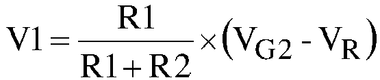
- For a working process and a principle of the charging
circuit 200 in the reverse charging time period, refer to the foregoing working process and principle of the chargingcircuit 200 in the forward charging time period. However, the reverse charging time period differs from the forward charging time period in that a current direction of the chargingcircuit 200 in the reverse charging time period is opposite to that in the forward charging time period, and is from the internal voltage VBUS to the external voltage VUSB. - For example, referring to a scenario shown in
FIG. 2D , the chargingcircuit 200 is applied to an Amobile phone 10. When the internal voltage VBUS is 20 V, the ratio of the first resistor R1 to the second resistor R2 is 5:4, the first switching transistor N1 is a Bi-GaN HEMT, and the second switching transistor N2 is a Si MOS transistor, the chargingcircuit 200 can control the first switching transistor N1 to be turned on under action of a gate-source voltage of 5 V, and control the second switching transistor N2 to be turned on under action of a gate-source voltage of 9 V. It should be noted that N1 and N2 are in the on state when the gate-source voltages are greater than the threshold voltages. In the scenario shown inFIG. 2D , the gate-source voltage V1 of N1 is stable at 5 V under control of the first drive voltage VG1, and the gate-source voltage of N2 is stable at 9 V under control of the second drive voltage VG2, in other words, N1 is turned on and works stably under action of the gate-source voltage of 5 V, and N2 is turned on and works stably under action of the gate-source voltage of 9 V. - Specifically, when N1 and N2 are turned on and work stably, as shown by an arrow in
FIG. 2D , the electronic device provides the internal voltage VBUS for the chargingcircuit 200, and outputs the external voltage VUSB by using N1 and N2 that are turned on. On a branch on which the arrow is located, the external voltage VUSB, the reference voltage VR, and the internal voltage VBUS are all 20 V. To keep N1 and N2 turned on, thegate driver 203 adjusts, for output, the second drive voltage VG2 to the first target drive voltage value 29 V based on the reference voltage VR. Therefore, the gate-source voltage of N2 is a value of the second drive voltage VG2 minus the reference voltage VR, and is equal to 9 V, and N2 is turned on and works under action of 9 V. In this case, because VG2 is 29 V, VR is 20 V, and the ratio of the first resistor R1 to the second resistor R2 is 5:4,
mobile phone 40 is charged by using the external voltage VUSB. - It can be learned from the foregoing descriptions that in the
charging circuit 200, in the reverse charging time period, the first drive voltage VG1 controls the first switching transistor N1 to be turned on, and the second drive voltage VG2 controls the second switching transistor N2 to be turned on. Because the voltage for controlling the first switching transistor N1 to be turned on and the voltage for controlling the second switching transistor N2 to be turned on are different, the gate-source voltage for driving the first switching transistor N1 to be turned on and the gate-source voltage for driving the second switching transistor N2 to be turned on are also different. Further, in an actual application, based on respective characteristics of the first switching transistor N1 and the second switching transistor N2, a first drive voltage VG1 that can enable the first switching transistor N1 to have smaller on impedance and lower power consumption may be selected, to control the first switching transistor N1 to be turned on, and similarly, a second drive voltage VG2 that can enable the second switching transistor N2 to have smaller on impedance and lower power consumption may be selected, to control the second switching transistor N2 to be turned on. Because both the first switching transistor N1 and the second switching transistor N2 are turned on under action of drive voltages adapted to the first switching transistor N1 and the second switching transistor N2, on impedance of the charging circuit is reduced, and reverse charging efficiency of the charging circuit is improved. - When the electronic device to which the
charging circuit 200 is applied does not need to supply power to an external electronic device or the electronic device receives a power supply stop instruction or the like, the chargingcircuit 200 needs to stop performing reverse charging (in other words, perform reverse turn-off). Specifically, referring toFIG. 2A (1), in a reverse turn-off scenario, thegate driver 203 in thecharging circuit 200 receives the reference voltage VR output by theswitch circuit 201, and adjusts the value of the second drive voltage VG2 to the second target drive voltage value based on the reference voltage VR, to control the second switching transistor N2 to be turned off. - For a principle and a process of adjusting the second drive voltage VG2 by the
gate driver 203 in the reverse turn-off time period, refer to the principle and the process of adjusting the second drive voltage VG2 by thegate driver 203 in the forward turn-off time period. Details are not described herein again. - The
gate driver 203 outputs the second drive voltage VG2 to the control terminal of N2 in theswitch circuit 201, so that after receiving the second drive voltage VG2, theswitch circuit 201 controls, under control of the second drive voltage VG2, the second switching transistor N2 to be turned off. Thegate driver 203 further outputs the second drive voltage VG2 to the second terminal of the second resistor R2 in thevoltage divider circuit 202. - In the reverse turn-off time period, the first terminal of the first resistor in the
voltage divider circuit 202 receives the reference voltage VR, and the second terminal of the second resistor R2 receives the second drive voltage VG2. Therefore, the voltage of the first terminal of the first resistor is VR, and the voltage of the second terminal of the second resistor R2 is VG2. A voltage between the voltages of the second terminal of the second resistor R2 and the first terminal of the first resistor R1 is divided by using R1 and R2, to obtain the first drive voltage VG1. The first drive voltage VG1 is a divided voltage between the reference voltage VR and the second drive voltage VG2. - For a working process and a principle of the
voltage divider circuit 202 in the reverse turn-off scenario, refer to the working process and the principle of thevoltage divider circuit 202 in the forward turn-off scenario. Details are not described herein again. - In the reverse turn-off time period, if the
gate driver 203 adjusts the value of the second drive voltage to be equal to the reference voltage VR, it can be ensured that the gate-source voltage of N2 is 0. Because the gate-source voltage of N2 is less than the threshold voltage, N2 can remain in the off state. After N2 is turned off, the reference voltage VR falls to 0, and thegate driver 203 correspondingly adjusts the second drive voltage VG2 to 0 V. The first drive voltage VG1 is a divided voltage between the reference voltage VR and the second drive voltage VG2. Therefore, the first drive voltage also falls to 0 V, and therefore the first switching transistor N1 is also turned off. - In the reverse turn-off scenario, the first terminal D1 of N1 of the
switch circuit 201 receives the internal voltage VBUS, the control terminal of N1 receives the first drive voltage VG1, the control terminal of N2 receives the second drive voltage VG2, and the reference voltage VR is output to thegate driver 203 at the first terminal of N2. The first switching transistor N1 is turned off under control of the first drive voltage VG1, and the second switching transistor N2 is turned off under control of the second drive voltage VG2. When the first switching transistor N1 and the second switching transistor N2 are turned off, the internal voltage VBUS cannot pass through N1 and N2 that are turned off to output the external voltage VUSB. In other words, a current inside the chargingcircuit 200 no longer flows from the internal voltage VBUS to the external voltage VUSB. - For example, in a scenario shown in
FIG. 2D , the chargingcircuit 200 repeatedly performs a process of performing reverse charging and then performing reverse turn-off. A voltage change in thecharging circuit 200 is shown inFIG. 2E . Specifically, referring toFIG. 2E , taking a reverse charging phase t1 as an example, when the internal voltage VBUS is 20 V, thegate driver 203 adjusts the second drive voltage VG2 to 29 V based on the reference voltage VR of 20 V. The first drive voltage VG1 is a divided voltage between the reference voltage VR and the second drive voltage VG2, and is 25 V. In this case, a gate-source voltage is 5 V, the gate-source voltage of N2 is 9 V, and both N1 and N2 are in the on state. Further, after receiving the internal voltage VBUS, the chargingcircuit 200 can output the output voltage VUSB of 20 V by using N1 and N2 that are turned on. Taking a reverse turn-off phase t2 as an example, in an initial phase of t2, N1 and N2 are not turned off, and the reference voltage is 20 V. In a scenario in which reverse charging is stopped, thegate driver 203 adjusts the second drive voltage VG2 to be equal to a value of the reference voltage, so that N2 is turned off. After N2 is turned off, the reference voltage falls to 0 V, and the second drive voltage VG2 falls to 0 V accordingly, so that N2 continues to be turned off. The first drive voltage VG1 is a divided voltage between the reference voltage VR and the second drive voltage VG2. Because both the second drive voltage and the reference voltage are 0 V, the first drive voltage VG1 is also 0 V, and further, N1 is turned off. Because N1 and N2 are turned off, the current inside the chargingcircuit 200 no longer flows from the internal voltage VBUS to the external voltage VUSB, and the external voltage VUSB is 0. - Referring to
FIG. 3A , an embodiment of this application discloses another chargingcircuit 300, including aswitch circuit 301, avoltage divider circuit 302, and agate driver 303. A structure and an operating principle of thegate driver 303 are the same as those of thegate driver 203 inFIG. 2A , a structure and an operating principle of thevoltage divider circuit 302 are the same as those of thevoltage divider circuit 202 inFIG. 2A , and a structure and an operating principle of theswitch circuit 301 are different from those of theswitch circuit 201 inFIG. 2A . Specifically, a structure of the chargingcircuit 300 inFIG. 3A is as follows:
Theswitch circuit 301 is separately connected to thevoltage divider circuit 302 and thegate driver 303, and theswitch circuit 303 includes a first switching transistor N1, a second switching transistor N2, and a third resistor R3. - A first terminal D1 of the first switching transistor N1 is connected to an external device (namely, a device other than an electronic device in which the
charging circuit 300 is located), and the first terminal D1 of the first switching transistor N1 receives, during forward charging, an external voltage VUSB provided by the external device, and provides the external voltage VUSB for the external device for charging during reverse charging. A second terminal D2 of the first switching transistor N1 is connected to a second terminal of the second switching transistor N2. A control terminal of the first switching transistor N1 receives a first drive voltage VG1. - The first drive voltage VG1 is used to drive the first switching transistor N1 to be turned on or control N1 to be turned off. A reference voltage VR is a basis reference when the
gate driver 303 adjusts a second drive voltage VG2. In this embodiment, the reference voltage VR is a voltage of a first terminal of the second switching transistor N2. In this embodiment, the reference voltage VR is the voltage of the first terminal of the second switching transistor N2. When the reference voltage VR is the voltage of the first terminal of the second switching transistor N2, a difference between the second drive voltage and the reference voltage is equivalent to a value of a gate-source voltage of N2. Therefore, using the reference voltage as a reference to adjust the second drive voltage VG2 can control N2 to be turned on or turned off. - The second terminal D2 of the first switching transistor N1 outputs an internal voltage VBUS during forward charging, and receives, during reverse charging, the internal voltage VBUS provided by an internal power supply of the electronic device.
- The internal voltage VBUS is a voltage of an internal node of the electronic device, and the internal node of the electronic device may be connected to an internal component of the electronic device. The internal component may be a power component, for example, a battery, or may be a component that needs to be powered, for example, a display screen or a speaker. The external voltage VUSB is a voltage of an external node of the electronic device, and the external node is connected to the external device. The external device may be a power supply device, for example, a power supply, or may be a component that needs to be powered, for example, a power bank or an external keyboard. In this embodiment of this application, the external node is the first terminal D1 of the first switching transistor N1, and the internal node is the second terminal D2 of the first switching transistor N1.
- It should be noted that for related descriptions of the internal voltage VBUS and the external voltage VBUS, refer to the foregoing content of the related descriptions of the internal voltage VBUS and the external voltage VBUS in
FIG. 2A . Details are not described herein again. - A control terminal of the second switching transistor N2 receives the second drive voltage VG2, and the first terminal of the second switching transistor N2 is grounded by using the third resistor R3. The first terminal of the second switching transistor N2 outputs the reference voltage VR. The second drive voltage VG2 is used to drive the second switching transistor N2 to be turned on or control N2 to be turned off.
- It should be noted that the first switching transistor N1 may be understood as a switching transistor, or may be understood as an equivalent switching transistor obtained after a plurality of switching transistors are connected in parallel. Similarly, the second switching transistor N2 may also be understood as a switching transistor, or may be understood as an equivalent switching transistor obtained after a plurality of switching transistors are connected in parallel. That the plurality of switching transistors are connected in parallel means that gates of the plurality of switching transistors are connected, sources of the plurality of switching transistors are connected, and drains of the plurality of switching transistors are connected. Specifically, for a parallel structure between the plurality of switching transistors, refer to 2011 shown in
FIG. 2A (2). - In some embodiments, the first switching transistor N1 is a Bi-GaN HEMT, and due to a characteristic of the Bi-GaN HEMT, each of the first terminal D1 and the second terminal D2 of the first switching transistor N1 can be used as a source or a drain. The control terminal of the first switching transistor N2 may be a gate.
- In some embodiments, the second switching transistor N2 is a Si MOS transistor. The first terminal of the second switching transistor N2 may be a source, the second terminal may be a drain, and the control terminal may be a gate.
- The
voltage divider circuit 302 is separately connected to thegate driver 303 and theswitch circuit 301, and thevoltage divider circuit 302 includes a first resistor R1 and a second resistor R2. A first terminal of the first resistor R1 receives the reference voltage VR, a second terminal of the first resistor R1 is connected to a first terminal of the second resistor R2, and a second terminal of the second resistor R2 receives the second drive voltage VG2. A common terminal between the first resistor R1 and the second resistor R2 outputs the first drive voltage VG1. A voltage value of the first drive voltage VG1 is a divided voltage value of the voltage difference between the reference voltage VR and the second drive voltage VG2. Specifically,
- It should be noted that R1 may be understood as a resistor, or R1 may be understood as an equivalent resistor obtained after a plurality of resistors are connected in series and/or in parallel, and a resistance value of R1 is a resistance value of the equivalent resistor. Similarly, R2 may also be understood as a resistor, or R2 may be understood as an equivalent resistor obtained after a plurality of resistors are connected in series and/or in parallel, and a resistance value of R2 is a resistance value of the equivalent resistor. For example, the second resistor R2 may also be shown in 202 in
FIG. 2A (3), to be specific, asecond resistor 2021 may be an equivalent resistor obtained after two resistors are connected in series. - It should be further noted that a specific structure in which a plurality of resistors are connected in series and/or in parallel is not limited in this embodiment of this application.
- For related descriptions of composition, a structure, and a working principle of the
voltage divider circuit 302, refer to thevoltage divider circuit 202 shown inFIG. 2A . - The
gate driver 303 is separately connected to theswitch circuit 301 and thevoltage divider circuit 302. Thegate driver 303 is configured to: in a forward charging or reverse charging process, receive the reference voltage VR output by theswitch circuit 301, and adjust a value of the second drive voltage VG2 to a first target drive voltage value based on the reference voltage VR, to control the second switching transistor N2 to be turned on. The second drive voltage VG2 is a drive voltage used to control N2 to be turned on or turned off. The first target drive voltage value is a value of the second drive voltage that can enable N2 to be in an on state. - In some other embodiments, the
gate driver 303 is further configured to: in a process of stopping forward charging or reverse charging, receive the reference voltage VR output by theswitch circuit 301, and adjust the value of the second drive voltage VG2 to a second target drive voltage value based on the reference voltage VR, to control the second switching transistor N2 to be turned off. The second target drive voltage value is a value of the second drive voltage that can enable N2 to be in an off state. - For related descriptions of composition and a connection structure of the
gate driver 303, refer to thegate driver 203 shown inFIG. 2A . - The following describes specific working processes of the charging
circuit 300. - Continuing to refer to
FIG. 3A , in a forward charging scenario of the chargingcircuit 300, thegate driver 303 in thecharging circuit 300 is configured to: receive the reference voltage VR, and adjust the value of the second drive voltage VG2 to the first target drive voltage value based on the reference voltage VR, to control the second switching transistor N2 to be turned on. - The first terminal of the first resistor R1 in the
voltage divider circuit 302 receives the reference voltage VR, the control terminal of the second switching transistor N2 receive the second drive voltage VG2, the voltage between the reference voltage VR and the second drive voltage VG2 is divided by using R1 and R2, to obtain the first drive voltage VG1. The first drive voltage VG1 is a divided voltage between the reference voltage VR and the second drive voltage VG2, and the value of the first drive voltage VG1 is
switch circuit 301 to be turned on or turned off. - It should be noted that for a working process and a principle of the
voltage divider circuit 302 in the forward charging time period, refer to the working process and the principle of thevoltage divider circuit 202 in the forward charging time period inFIG. 2A . Details are not described herein again. - In the forward charging scenario, the
switch circuit 301 receives the external voltage VUSB by using the first terminal of N1, receives the first drive voltage VG1 by using the control terminal of N1, receives the second drive voltage VG2 by using the control terminal of N2, and outputs the reference voltage VR to thegate driver 303 by using a common terminal between the first terminal of the second switching transistor N2 and the third resistor. The first switching transistor N1 is turned on under control of the first drive voltage VG1, and the second switching transistor N2 is turned on under control of the second drive voltage VG2. When the first switching transistor N1 and the second switching transistor N2 are turned on, the external voltage VUSB passes through N1 that is turned on to obtain and output the internal voltage VBUS. In other words, a current inside the chargingcircuit 200 flows from the external voltage VUSB to the internal voltage VBUS. - Because the value of the second drive voltage VG2 output by the
gate driver 303 is adjusted based on the reference voltage VR, the value (namely, the difference between the second drive voltage and the reference voltage VR) of the gate-source voltage applied to N2 can always be greater than a threshold voltage of N2, so that N2 is in the on state. For a specific process and principle of controlling the second switching transistor N2 to be turned on by thegate driver 303, refer to the foregoing process and principle of controlling N2 to be turned on by thegate driver 202 inFIG. 2A . Details are not described herein again. - For example, if the first target drive voltage value may be a sum of the reference voltage VR and a first drive value, a process of turning on N1 in the forward charging scenario is as follows: The second terminal D2 of N1 is a source of N1, a voltage of the second terminal D2 of N1 at an initial moment is 0, a value of a gate-source voltage (namely, a voltage between the control terminal of N1 and the second terminal D2 of N1) of N1 is equivalent to the value of the first drive voltage VG1, and a calculation formula for the first drive voltage VG1 is


- It can be learned from the calculation formula for V1 that because the difference between the second drive voltage and the reference voltage is the first drive value, and is a fixed value, and resistance values of R1 and R2 remain unchanged, a value of V1 remains unchanged, and the first switching transistor N1 is still in the on state.
- Specifically, referring to a scenario shown in
FIG. 3B , the chargingcircuit 300 is applied to an Amobile phone 10. When the external voltage VUBS is 20 V, a ratio of the first resistor R1 to the second resistor R2 is 5:4, the first switching transistor N1 is a Bi-GaN HEMT, and the second switching transistor N2 is a Si MOS transistor, the chargingcircuit 300 can control the first switching transistor N1 to be turned on under action of a gate-source voltage of 5 V, and control the second switching transistor N2 to be turned on under action of a gate-source voltage of 9 V. It should be noted that N1 and N2 are in the on state when the gate-source voltages are greater than the threshold voltages. In the scenario shown inFIG. 3B , under control of VG, the gate-source voltage of N1 is stable at 5 V, and the gate-source voltage of N2 is stable at 9 V, in other words, N1 is turned on and works stably under action of the gate-source voltage of 5 V, and N2 is turned on and works stably under action of the gate-source voltage of 9 V. - When N1 and N2 are turned on and work stably, as shown by an arrow in
FIG. 3B , an external power supply provides the external voltage VUSB for the chargingcircuit 300, and the internal voltage VBUS is output by using N1 that is turned on. On a branch on which the arrow is located, both the external voltage VUSB and the internal voltage VBUS are 20 V. Because N2 is also in the on state, the reference voltage VR is also 20 V. To keep N1 and N2 turned on, thegate driver 303 adjusts the second drive voltage VG2 to 29 V based on the reference voltage VR. Therefore, the gate-source voltage of N2 is 9 V, and N2 is turned on and works under action of 9 V. In this case, because the second drive voltage VG2 is 29 V, VR is 20 V, the ratio of the first resistor R1 to the second resistor R2 is 5:4, and the first drive voltage is
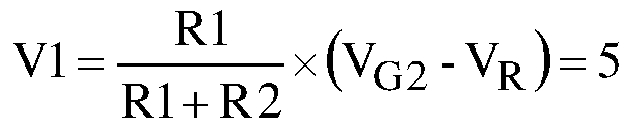
circuit 300 may provide the internal voltage VBUS for the inside of the electronic device, to charge the inside of the electronic device, and the Amobile phone 10 is in a charging state. - It can be learned from the foregoing descriptions that in the
charging circuit 300, the first drive voltage VG1 controls the first switching transistor N1 to be turned on, and the second drive voltage VG2 controls the second switching transistor N2 to be turned on. Because the voltage for controlling the first switching transistor N1 to be turned on and the voltage for controlling the second switching transistor N2 to be turned on may be different, a value of the gate-source voltage for driving the first switching transistor N1 to be turned on and a value of the gate-source voltage for driving the second switching transistor N2 to be turned on may also be different. In an actual application, based on respective characteristics of the first switching transistor N1 and the second switching transistor N2, a first drive voltage VG1 that can enable the first switching transistor N1 to have smaller on impedance and lower power consumption may be selected, to control the first switching transistor N1 to be turned on, and similarly, a second drive voltage VG2 that can enable the second switching transistor N2 to have smaller on impedance and lower power consumption may be selected, to control the second switching transistor N2 to be turned on. Because both the first switching transistor N1 and the second switching transistor N2 are turned on under action of drive voltages adapted to the first switching transistor N1 and the second switching transistor N2, on impedance of the charging circuit is reduced, and forward charging efficiency of the charging circuit is improved. - Compared with the charging
circuit 200, the chargingcircuit 300 mainly differs in that the external voltage VUSB is transmitted to a branch of the internal voltage VBUS that implements a forward charging action, and the current passes through only the first switching transistor N1. Because the branch passes through only one switching transistor, compared with the chargingcircuit 200, during forward charging, on impedance of the branch is smaller, forward charging efficiency is higher, and power consumption is lower. - When the electronic device to which the
charging circuit 300 is applied is fully charged or the electronic device receives a charging stop instruction or the like, the chargingcircuit 300 needs to stop performing forward charging. Specifically, referring toFIG. 3A , in a forward turn-off scenario, thegate driver 303 in thecharging circuit 300 receives the reference voltage VR output by theswitch circuit 301, and adjusts the value of the second drive voltage VG2 to the second target drive voltage value based on the reference voltage VR, to control the second switching transistor N2 to be turned off. - Specifically, for a principle and a working process of the
gate driver 303 in the forward turn-off time period, refer to the principle and the working process of thegate driver 203 shown inFIG. 2A in the forward turn-off time period. Details are not described herein again. - The
voltage divider circuit 302 receives the reference voltage VR by using the first terminal of the first resistor R1, receives the second drive voltage VG2 by using the second terminal of the second resistor R2, and then divides the voltage between the reference voltage VR and the second drive voltage VG2 by using R1 and R2, to obtain the first drive voltage VG1. The first drive voltage VG1 is a divided voltage between the reference voltage VR and the second drive voltage VG2, and the value of the first drive voltage VG1 is
switch circuit 301 to be turned off. Specifically, for a principle in a working process of thevoltage divider circuit 302 and the working process in the forward turn-off time period, refer to the principle in the working process of thevoltage divider circuit 202 shown inFIG. 2A and the working process in the forward turn-off time period. Details are not described herein again. - In the forward turn-off scenario, the
switch circuit 301 receives the external voltage VUSB by using the first terminal D1 of N1, receives the first drive voltage VG1 by using the control terminal of N1, receives the second drive voltage VG2 by using the control terminal of N2, and outputs the reference voltage VR to thegate driver 303 by using a common terminal between the first terminal of the second switching transistor N2 and the third resistor. The second switching transistor N2 is turned off under control of the second drive voltage VG2, and further, the first switching transistor N1 is also turned off under control of the first drive voltage VG1. When the first switching transistor N1 is turned off, the external voltage VUSB cannot pass through N1 to output a current, and therefore output of the internal voltage VBUS is stopped. In other words, the current inside the chargingcircuit 200 no longer flows from the external voltage VUSB to the internal voltage VBUS through N1. - For example, if the
gate driver 303 adjusts, in the forward turn-off scenario, the second drive voltage VG2 to be equal to the reference voltage VR, the gate-source voltage of N2 is 0, and N2 may be controlled to be in the off state. After N2 is turned off, the first terminal of N2 is grounded, and the reference voltage VR falls to 0 V. Therefore, the second drive voltage VG2 also decreases with the reference voltage VR, and also falls to 0 V. In addition, the first drive voltage VG1 is a divided voltage between the second drive voltage VG2 and the reference voltage VR. When both the second drive voltage VG2 and the reference voltage VR are 0 V, the first drive voltage VG1 is also 0 V, and the first switching transistor N1 is turned off under control of the first drive voltage VG1 of 0 V. Therefore, in the forward turn-off scenario, N2 is controlled, by using the second drive voltage, to be turned off, so that the first drive voltage can control N1 to be turned off. - For example, in a scenario shown in
FIG. 3B , the chargingcircuit 300 repeatedly performs a process of performing forward charging and then performing forward turn-off. A voltage change in thecharging circuit 300 is shown inFIG. 3C . Specifically, referring toFIG. 3C , taking a forward charging phase t1 as an example, the external voltage VUSB provided by an external power supply for the chargingcircuit 300 is 20 V, and thegate driver 303 adjusts the second drive voltage VG2 to 29 V based on the reference voltage VR. Because the first drive voltage VG1 is a divided voltage between the second drive voltage VG2 and the reference voltage VR, and a ratio of the first resistor R1 to the second resistor R2 is 5:4. Therefore, the first drive voltage is 25 V. In this case, both N1 and N2 are in the on state, so that the external voltage VUSB can pass through N1 that is turned on to output the internal voltage VBUS of 20 V. Taking a forward turn-off phase t2 as an example, the external voltage VUSB received by the chargingcircuit 200 is 20 V, and the second drive voltage VG2 falls to 0 V along with the reference voltage VR in the forward turn-off scenario, so that N1 is turned off. Because the first drive voltage is a divided voltage between the second drive voltage and the reference voltage, the first drive voltage also changes to 0 V, so that N1 is also turned off. Because N1 and N2 are turned off, the current inside the chargingcircuit 200 no longer flows from the external voltage VUSB to the internal voltage VBUS, and the internal voltage VBUS is 0. - Continuing to refer to
FIG. 3A , in a reverse charging scenario of the chargingcircuit 30, thegate driver 303 in thecharging circuit 300 is configured to: receive the reference voltage VR, and adjust the value of the second drive voltage VG2 to the first target drive voltage value based on the reference voltage VR, to control the second switching transistor N2 to be turned on. - For a working process and a principle of the
gate driver 303 in the reverse charging time period, refer to the related descriptions of thegate driver 303 in the forward charging time period. Details are not described herein again. - In the reverse charging time period, the
voltage divider circuit 302 receives the reference voltage VR by using the first terminal of the first resistor R1, receives the second drive voltage VG2 by using the second terminal of the second resistor R2, and divides the voltage difference between the reference voltage VR and the second drive voltage VG2 by using R1 and R2, to obtain the first drive voltage VG1. - For a working process and a principle of the
voltage divider circuit 302 in the reverse charging time period, refer to the related descriptions of thevoltage divider circuit 302 in the forward charging time period. Details are not described herein again. - In the reverse charging scenario, the
switch circuit 301 receives the internal voltage VBUS by using the second terminal of the first switching transistor N1, receives the first drive voltage VG1 by using the control terminal of N1, receives the second drive voltage VG2 by using the control terminal of N2, and outputs the reference voltage VR to thegate driver 303 by using the first terminal of N2. The first switching transistor N1 is turned on under control of the first drive voltage VG1, and the second switching transistor N2 is turned on under control of the second drive voltage VG2. When the first switching transistor N1 and the second switching transistor N2 are turned on, the internal voltage VBUS received by the second terminal of N1 passes through N1 that is turned on to output the external voltage VUSB from the second terminal of N1. In other words, a current inside the chargingcircuit 300 flows from the internal voltage VBUS to the external voltage VUSB. For a turn-on process and a principle of the second switching transistor N2 in the reverse charging scenario, refer to the foregoing related descriptions of the process of turning on N2 in the forward charging scenario inFIG. 3A . Details are not described herein again. - In the reverse charging scenario, a process in which the first drive voltage VG1 controls the first switching transistor N1 of the
switch circuit 301 to be turned on is as follows: At an initial moment of reverse charging, N1 is in the off state. In this case, the first terminal D1 of N1 is used as a source of N1, a voltage of the first terminal D1 is initially 0 V, and no external voltage is output. In this case, thevoltage divider circuit 202 provides the first drive voltage

- It should be noted that a working process and a principle in the reverse charging scenario are similar to those during forward charging, and a main difference is that a current direction is opposite to that in the forward charging scenario, and is from the internal voltage VBUS to the external voltage VUSB. For the working process in the reverse charging scenario, also refer to the foregoing descriptions in the forward charging scenario in
FIG. 3A - For example, referring to a scenario shown in
FIG. 3D , the chargingcircuit 300 is applied to an Amobile phone 10. When the internal voltage VBUS is 20 V, a ratio of the first resistor R1 to the second resistor R2 is 5:4, the first switching transistor N1 is a Bi-GaN HEMT, and the second switching transistor N2 is a Si MOS transistor, the chargingcircuit 300 can control the first switching transistor N1 to be turned on under action of a gate-source voltage of 5 V, and control the second switching transistor N2 to be turned on under action of a gate-source voltage of 9 V. It should be noted that N1 and N2 are in the on state when the gate-source voltages are greater than threshold voltages. In the scenario shown inFIG. 3D , under control of VG, the gate-source voltage of N1 is stable at 5 V, and the gate-source voltage of N2 is stable at 9 V, in other words, N1 is turned on and works stably under action of the gate-source voltage of 5 V, and N2 is turned on and works stably under action of the gate-source voltage of 9 V. - Specifically, when N1 and N2 are turned on and work stably, as shown by an arrow in
FIG. 3D , an internal power supply of the electronic device provides the internal voltage VBUS for the chargingcircuit 300, and outputs the external voltage VUSB by using N1 that is turned on. On a branch on which the arrow is located, the external voltage VUSB, the reference voltage VR, and the internal voltage VBUS are all 20 V. To keep N1 and N2 opened, thegate driver 303 adjusts the second drive voltage VG2 to the first target drive voltage value 29 V based on the reference voltage VR, and therefore, the gate-source voltage of N2 is 9V, and N2 is turned on and works under action of 9 V. In this case, because VG2 is 29 V, VR is 20 V, the ratio of the first resistor R1 to the second resistor R2 is 5:4, and the first drive voltage is

- It can be learned from the foregoing descriptions that in the
charging circuit 300, in the reverse charging time period, the first drive voltage VG1 controls the first switching transistor N1 to be turned on, and the second drive voltage VG2 controls the second switching transistor N2 to be turned on. Because the voltage for controlling the first switching transistor N1 to be turned on and the voltage for controlling the second switching transistor N2 to be turned on may be different, a value of the gate-source voltage for driving the first switching transistor N1 to be turned on and a value of the gate-source voltage for driving the second switching transistor N2 to be turned on may also be different. In an actual application, based on respective characteristics of the first switching transistor N1 and the second switching transistor N2, a first drive voltage VG1 that can enable the first switching transistor N1 to have smaller on impedance and lower power consumption may be selected, to control the first switching transistor N1 to be turned on, and similarly, a second drive voltage VG2 that can enable the second switching transistor N2 to have smaller on impedance and lower power consumption may be selected, to control the second switching transistor N2 to be turned on. Because both the first switching transistor N1 and the second switching transistor N2 are turned on under action of drive voltages adapted to the first switching transistor N1 and the second switching transistor N2, on impedance of the charging circuit is reduced, and reverse charging efficiency of the charging circuit is improved. - Compared with the charging
circuit 200, the chargingcircuit 300 mainly differs in that the internal voltage VBUS is transmitted to a branch of the external voltage VUSB that implements a reverse charging action, and the current passes through only the first switching transistor N1. Because the branch passes through only one switching transistor, compared with the chargingcircuit 200, during reverse charging, on impedance of the branch is smaller, reverse charging efficiency is higher, and power consumption is lower. - When the electronic device to which the
charging circuit 300 is applied does not need to supply power to an external electronic device or the electronic device receives a power supply stop instruction or the like, the chargingcircuit 300 needs to stop performing reverse charging (in other words, perform reverse turn-off). Specifically, referring toFIG. 3A , in a reverse turn-off scenario, thegate driver 303 in thecharging circuit 300 receives the reference voltage VR output by theswitch circuit 301, and adjusts the value of the second drive voltage VG2 to the second target drive voltage value based on the reference voltage VR, to control the second switching transistor N2 to be turned off. - The second drive voltage VG2 output by the
gate driver 303 is output to theswitch circuit 301, so that after receiving the second drive voltage VG2, theswitch circuit 301 controls, under control of the second drive voltage VG2, the second switching transistor N2 to be turned off. The second drive voltage VG2 output by thegate driver 303 is further received by the second terminal of the second resistor of thevoltage divider circuit 302. - For a principle and a working process of the
gate driver 303 in the reverse turn-off time period, refer to the principle and the working process of thegate driver 303 in the forward turn-off time period. Details are not described herein again. - In the reverse turn-off scenario, the
voltage divider circuit 302 receives the reference voltage VR by using the first terminal of the first resistor R1, receives the second drive voltage VG2 by using the second terminal of the second resistor R2, and divides the voltage difference between the reference voltage VR and the second drive voltage VG2 by using R1 and R2, to obtain the first drive voltage VG1. The first drive voltage VG1 can control the first switching transistor N1 of theswitch circuit 201 to be turned off. - For a working process and a principle of the
voltage divider circuit 302 in the reverse turn-off scenario, refer to the working process and the principle of thevoltage divider circuit 302 in the forward turn-off scenario. Details are not described herein again. - For a principle about why and a process in which the first drive voltage VG1 can control the first switching transistor N1 of the
switch circuit 301 to be turned off in the reverse turn-off time period, refer to the foregoing related content in which the first drive voltage VG1 can control, in the forward turn-off scenario, the first switching transistor N1 of theswitch circuit 301 to be turned off. Details are not described herein again. - For a principle about why and a process in which the second drive voltage VG2 can control the second switching transistor N2 of the
switch circuit 301 to be turned off in the reverse turn-off time period, refer to the foregoing related content in which the second drive voltage VG2 can control, in the forward turn-off time period, the second switching transistor N2 of theswitch circuit 301 to be turned off. Details are not described herein again. - In the reverse turn-off time period, the
switch circuit 301 receives the internal voltage VBUS by using the second terminal D2 of N1, receives the first drive voltage VG1 by using the control terminal of N1, receives the second drive voltage VG2 by using the control terminal of N2, and outputs the reference voltage VR by using a common terminal between the first terminal of the second switching transistor N2 and the third resistor. The first switching transistor N1 is turned off under control of the first drive voltage VG1, and the second switching transistor N2 is turned off under control of the second drive voltage VG2. When the first switching transistor N1 and the second switching transistor N2 are turned off, the internal voltage VBUS cannot pass through N1 to obtain and output the external voltage VUSB. In other words, a current inside the chargingcircuit 300 no longer flows from the internal voltage VBUS to the external voltage VUSB. - For example, in a scenario shown in
FIG. 3D , the chargingcircuit 300 repeatedly performs a process of performing reverse charging and then performing reverse turn-off. A voltage change in thecharging circuit 300 is shown inFIG. 3E . Specifically, referring toFIG. 3E , taking a reverse charging phase t1 as an example, the internal voltage VBUS received by the chargingcircuit 300 is 20 V, and thegate driver 303 adjusts the second drive voltage VG2 to 29 V based on the reference voltage VR. The first drive voltage VG1 is a divided voltage between the reference voltage VR and the second drive voltage VG2, and is 25 V. In this case, both N1 and N2 are in the on state, and therefore the internal voltage VBUS can pass through N1 that is turned on to output the external voltage VUSB of 20 V. Taking a reverse turn-off phase t2 as an example, the internal voltage VBUS received by the chargingcircuit 300 is 20 V, and the second drive voltage VG2 falls to 0 V along with the reference voltage VR in a scenario in which reverse charging is stopped, so that N2 is turned off. The first drive voltage VG1 is a divided voltage between the second drive voltage VG2 and the reference voltage VR. Because both the second drive voltage VG2 and the reference voltage VR fall to 0 V, the first drive voltage VG1 also changes to 0 V, so that N1 is turned off. Because N1 is turned off, the current inside the chargingcircuit 300 no longer flows from the internal voltage VBUS to the external voltage VUSB, and the external voltage VUSB is 0. - It can be learned from
FIG. 2A andFIG. 3A that in both the chargingcircuit 200 and the chargingcircuit 300, the switch circuit can output the reference voltage to the gate driver in the forward charging time period, the reverse charging time period, the forward turn-off time period, or the reverse turn-off time period, and in the forward charging time period or the reverse charging time period, the switch circuit can control, by using the first drive voltage, the first switching transistor to be turned on, and control, by using the second drive voltage, the second switching transistor to be turned on. Therefore, both the first switching transistor N1 and the second switching transistor N2 are turned on, by using the first drive voltage and the second drive voltage that are different, under action of gate-source voltages suitable for the first switching transistor N1 and the second switching transistor N2, so that on impedance of the charging circuit is reduced, and bidirectional charging efficiency of the charging circuit is improved. - In the forward turn-off time period or the reverse turn-off time period, the switch circuit may further control, by using the first drive voltage, the first switching transistor to be turned off, and control, by using the second drive voltage, the second switching transistor to be turned off. When N1 and N2 are turned off, forward charging or reverse charging may be stopped.
- Specifically, in the forward charging time period, the switch circuit in
FIG. 2A receives the external voltage, and outputs the internal voltage to the inside of the electronic device by using the first switching transistor and the second switching transistor that are turned on, in the reverse charging time period, the switch circuit receives the internal voltage, and outputs the external voltage to the outside of the electronic device by using the first switching transistor and the second switching transistor that are turned on, in the forward turn-off time period, the switch circuit receives the external voltage, and stops outputting the internal voltage to the inside of the electronic device by using the first switching transistor and the second switching transistor that are turned off, and in the reverse turn-off time period, the switch circuit receives the internal voltage, and stops outputting the external voltage to the outside of the electronic device by using the first switching transistor and the second switching transistor that are turned off. In other words, the first switching transistor and the second switching transistor that are turned on need to be used to implement charging, and the first switching transistor and the second switching transistor that are turned off need to be used to implement turn-off. - In the forward charging time period, the switch circuit in
FIG. 3A receives the external voltage, and outputs the internal voltage to the inside of the electronic device by using the first switching transistor that is turned on, in the reverse charging time period, the switch circuit receives the internal voltage, and outputs the external voltage to the outside of the electronic device by using the first switching transistor that is turned on, in the forward turn-off time period, the switch circuit receives the external voltage, and stops outputting the internal voltage to the inside of the electronic device by using the first switching transistor that is turned off, and in the reverse turn-off time period, the switch circuit receives the internal voltage, and stops outputting the external voltage to the outside of the electronic device by using the first switching transistor that is turned off. In other words, only the first switching transistor that is turned on needs to be used to implement charging, and only the second switching transistor that is turned off needs to be used to implement turn-off. It can be learned fromFIG. 2A andFIG. 3A that in the forward charging time period, the reverse charging time period, the forward turn-off time period, or the reverse turn-off time period, the voltage divider circuits inFIG. 2A andFIG. 3A are configured to perform voltage division by using the reference voltage and the second drive voltage, to obtain and output the first drive voltage. It can be learned fromFIG. 2A andFIG. 3A that the gate drivers inFIG. 2A andFIG. 3A adjust and output the second drive voltage based on the reference voltage in the forward charging time period or the reverse charging time period, and also adjust and output the second drive voltage based on the reference voltage in the forward turn-off time period or the reverse turn-off time period. However, specific manners of adjusting the second drive voltage in the charging time period and the turn-off time period are different. Specifically, in the forward charging time period or the reverse charging time period, the value of the second drive voltage is adjusted to the sum of the reference voltage and the first drive value, and the second drive voltage is output, but in the forward turn-off time period or the reverse turn-off time period, the value of the second drive voltage is adjusted to the value of the reference voltage, and the second drive voltage is output. - It can be learned based on the descriptions in
FIG. 2A andFIG. 3A that in the charging circuit provided in the embodiments, the switch circuit is configured to: receive a power supply voltage and a plurality of drive voltages, and output a reference voltage and an output voltage of the charging circuit. The plurality of drive voltages include a first drive voltage and a second drive voltage. The voltage divider circuit is configured to: receive the second drive voltage and the reference voltage, and output the first drive voltage. The gate driver is configured to: receive the reference voltage, and output the second drive voltage. - The power supply voltage is a voltage supplying power to the charging circuit. The output voltage of the charging circuit is a voltage provided by the charging circuit for a component that needs to be powered. The power supply voltage may be the external voltage mentioned in
FIG. 2A andFIG. 3A in a forward charging time period, and may be an internal voltage in a reverse charging time period. The output voltage of the charging circuit is the internal voltage in the forward charging time period, and is the external voltage in the reverse charging time period. The external voltage is a voltage of an external node in the charging circuit, and the internal voltage is a voltage of an internal node in the charging circuit. The power supply voltage is the external voltage in a forward turn-off time period, and is the internal voltage in a reverse turn-off time period. The output voltage of the charging circuit is the internal voltage in the forward turn-off time period, and is the external voltage in the reverse turn-off time period. - In embodiments of this application, the switch circuit can obtain the first drive voltage and the second drive voltage by using the gate driver and the voltage divider circuit, and voltage values of the first drive voltage and the second drive voltage may be different. Therefore, the switch circuit may use a proper first drive voltage and a proper second drive voltage, to reduce on impedance of the charging circuit and improve bidirectional charging efficiency of the charging circuit.
- Based on the foregoing
FIG. 2B ,FIG. 2D ,FIG. 3B , andFIG. 3D , an embodiment of this application further discloses a charging system. The charging system includes at least a first electronic device, the first electronic device includes a charging management module, and the charging management module includes any one of the charging circuits provided in the foregoing embodiments of this application. The charging system further includes a charger connected to the first electronic device and/or a second electronic device connected to the first electronic device. The charger connected to the first electronic device is configured to output a power supply voltage to the first electronic device, and the second electronic device connected to the first electronic device is configured to receive an output voltage of the charging circuit. - Referring to
FIG. 4 , an embodiment of this application further discloses anelectronic device 400. Theelectronic device 400 may be a tablet computer, a desktop computer, a laptop computer, a notebook computer, an ultra-mobile personal computer (Ultra-mobile Personal Computer, UMPC), a handheld computer, a netbook, a personal digital assistant (Personal Digital Assistant, PDA), a wearable electronic device, or the like. Theelectronic device 400 includes aprocessor 401, acharging management module 402, apower management module 403, and a USB interface 404. Thecharging management module 402 includes acharging circuit 4021. - It may be understood that the structure illustrated in this embodiment does not constitute a specific limitation on the
electronic device 400. In some other embodiments, theelectronic device 400 may include more or fewer components than those shown in the figure, or may combine some components, or may split some components, or may have different component arrangements. The components shown in the figure may be implemented by using hardware, software, or a combination of software and hardware. - The
processor 401 may include one or more processing units. For example, the processor 110 may include an application processor (application processor, AP), a modem processor, a graphics processing unit (graphics processing unit, GPU), an image signal processor (image signal processor, ISP), a controller, a video codec, a digital signal processor (digital signal processor, DSP), a baseband processor, and/or a neural-network processing unit (neural-network processing unit, NPU). Different processing units may be independent components, or may be integrated into one or more processors. For example, in this application, theprocessor 401 may control thecharging circuit 4021 to perform forward charging, reverse charging, stop forward charging, or stop reverse charging. - The
charging management module 402 is configured to: receive, from the charger, an external voltage VUSB input through charging, or provide an external voltage VUSB to the outside. The charger may be a wireless charger or a wired charger. In some embodiments of wired charging, thecharging management module 402 may receive, by using the USB interface 404, the external voltage VUSB input by the wired charger through charging, or provide the external voltage VUSB to the outside. In this embodiment of this application, thecharging circuit 4021 in thecharging management module 402 may be configured to: receive the external voltage VUSB input through charging, and input the internal voltage VBUS, and may also be configured to: receive the internal voltage VBUS, and output the external voltage VUSB. Specifically, for a specific working process, principle, and structure of thecharging circuit 4021, refer to the foregoing chargingcircuit 200 shown inFIG. 2A and the foregoing chargingcircuit 300 shown inFIG. 3A . Details are not described herein again. - The
power management module 403 is configured to connect to a battery, thecharging management module 402, and theprocessor 401. In this embodiment of this application, thepower management module 403 receives the internal voltage VBUS input by thecharging management module 402, and supplies power to the processor, an internal memory, a display screen, a camera, or the like, or receives the internal voltage VBUS input by the battery, and inputs the internal voltage VBUS to thecharging management module 402. - The USB interface 404 is an interface that complies with USB standard specifications, and may be specifically a Mini USB interface, a Micro USB interface, a USB Type C interface, or the like. In this embodiment of this application, the USB interface 404 may be configured to connect to a charger to provide the external voltage VUSB for the
charging circuit 4021, and may also be configured to receive the external voltage VUSB output by thecharging circuit 4021. - Through the descriptions of the foregoing implementations, a person skilled in the art may clearly understand that, for the purpose of convenient and brief description, only division of the foregoing functional modules is used as an example for description. In an actual application, the functions may be allocated to and completed by different functional modules based on a requirement. In other words, an internal structure of the apparatus is divided into different functional modules, to complete all or some of the functions described above. For a specific working process of the system, apparatus, and unit described above, refer to a corresponding process in the foregoing method embodiments. Details are not described herein again.
- In the several embodiments provided in the embodiments, it should be understood that the disclosed system, apparatus, and method may be implemented in other manners. For example, the described apparatus embodiment is merely an example. For example, the module or unit division is merely logical function division, and there may be another division manner in actual implementation. For example, a plurality of units or components may be combined or integrated into another system, or some features may be ignored or not performed. In addition, the displayed or discussed mutual couplings or direct couplings or communication connections may be implemented through some interfaces. The indirect couplings or communication connections between the apparatuses or units may be implemented in an electrical form, a mechanical form, or another form.
- The units described as separate components may or may not be physically separated, and components displayed as units may or may not be physical units, in other words, may be located in one place, or may be distributed on a plurality of network units. Some or all of the units may be selected based on actual requirements to achieve the objectives of the solutions in embodiments. In addition, functional units in the embodiments may be integrated into one processing unit, or each of the units may exist alone physically, or two or more units may be integrated into one unit. The integrated unit may be implemented in a form of hardware, or may be implemented in a form of a software functional unit.
- When the integrated unit is implemented in the form of the software functional unit and sold or used as an independent product, the integrated unit may be stored in a computer-readable storage medium. Based on such an understanding, the technical solutions of the embodiments essentially, or the part contributing to the conventional technology, or all or some of the technical solutions may be implemented in a form of a software product. The computer software product is stored in a storage medium and includes several instructions for instructing a computer device (which may be a personal computer, a server, a network device, or the like) or a processor to perform all or some of the steps of the methods described in the embodiments. The foregoing storage medium includes any medium that can store program code, such as a flash memory, a removable hard disk, a read-only memory, a random access memory, a magnetic disk, or an optical disc.
- The foregoing descriptions are merely specific implementations of this application, but are not intended to limit the protection scope of this application. Any change or replacement made within the technical scope disclosed in this application shall fall within the protection scope of this application. Therefore, the protection scope of this application shall be subject to the protection scope of the claims.
Claims (20)
- A charging circuit, comprising:a switch circuit, a voltage divider circuit, and a gate driver, wherein the switch circuit is separately connected to the voltage divider circuit and the gate driver, and the voltage divider circuit is connected to the gate driver, whereinthe switch circuit is configured to: receive a power supply voltage and a plurality of drive voltages, and output a reference voltage and an output voltage of the charging circuit, wherein the plurality of drive voltages comprise a first drive voltage and a second drive voltage;the voltage divider circuit is configured to: receive the second drive voltage and the reference voltage, and output the first drive voltage; andthe gate driver is configured to: receive the reference voltage, and output the second drive voltage, wherein a voltage value of the second drive voltage is different from a voltage value of the first drive voltage.
- The charging circuit according to claim 1, wherein when receiving the second drive voltage and the reference voltage, and outputting the first drive voltage, the voltage divider circuit is configured to:
receive the second drive voltage and the reference voltage, and perform voltage division on the second drive voltage and the reference voltage to obtain the first drive voltage. - The charging circuit according to claim 2, wherein the voltage divider circuit comprises:a first resistor and a second resistor, whereina first terminal of the first resistor receives the reference voltage, and the first terminal of the first resistor is connected to a first terminal of the second resistor; andthe first terminal of the second resistor receives the second drive voltage, and a common terminal between the first resistor and the second resistor outputs the first drive voltage.
- The charging circuit according to any one of claims 1 to 3, wherein when receiving the reference voltage, and outputting the second drive voltage, the gate driver is configured to:
receive the reference voltage, adjust the second drive voltage based on the reference voltage, and output the second drive voltage. - The charging circuit according to any one of claims 1 to 4, wherein when receiving the reference voltage, and outputting the second drive voltage, the gate driver is configured to:
adjust the second drive voltage to a first target drive value based on the reference voltage and output the second drive voltage in a forward charging time period or a reverse charging time period. - The charging circuit according to claim 5, wherein the first target drive value is a sum of the reference voltage and a first drive value.
- The charging circuit according to claim 5 or 6, wherein the gate driver is further configured to:
adjust the second drive voltage to a second target drive value based on the reference voltage and output the second drive voltage in a forward turn-off time period or a reverse turn-off time period. - The charging circuit according to claim 7, wherein the second target drive value is equal to the reference voltage.
- The charging circuit according to any one of claims 1 to 8, wherein when receiving the power supply voltage and the plurality of drive voltages, and outputting the reference voltage and the output voltage of the charging circuit, the switch circuit is configured to:
receive the power supply voltage and the plurality of drive voltages and output the reference voltage and the output voltage of the charging circuit under control of the plurality of drive voltages in the forward charging time period or the reverse charging time period. - The charging circuit according to claim 9, wherein when receiving the power supply voltage and the plurality of drive voltages and outputting the reference voltage and the output voltage of the charging circuit under control of the plurality of drive voltages in the forward charging time period or the reverse charging time period, the switch circuit is configured to:receive an external voltage and the plurality of drive voltages and output the reference voltage and an internal voltage under control of the plurality of drive voltages in the forward charging time period; andreceive the internal voltage and the plurality of drive voltages and output the reference voltage and the external voltage under control of the plurality of drive voltages in the reverse charging time period, wherein the power supply voltage is the external voltage in the forward charging time period, and is the internal voltage in the reverse charging time period, the output voltage of the charging circuit is the internal voltage in the forward charging time period, and is the external voltage in the reverse charging time period, the external voltage is a voltage of an external node in the charging circuit, and the internal voltage is a voltage of an internal node in the charging circuit.
- The charging circuit according to claim 9 or 10, wherein the switch circuit is further configured to:
receive the power supply voltage and the plurality of drive voltages and stop outputting the reference voltage and the output voltage of the charging circuit under control of the plurality of drive voltages in the forward turn-off time period or the reverse turn-off time period. - The charging circuit according to claim 11, wherein when receiving the power supply voltage and the plurality of drive voltages and stopping outputting the reference voltage and the output voltage of the charging circuit under control of the plurality of drive voltages in the forward turn-off time period or the reverse turn-off time period, the switch circuit is configured to:receive the external voltage and the plurality of drive voltages and stop outputting the reference voltage of the charging circuit and the internal voltage under control of the plurality of drive voltages in the forward turn-off time period; andreceive the internal voltage and the plurality of drive voltages and stop outputting the reference voltage and the external voltage under control of the plurality of drive voltages in the reverse turn-off time period, whereinthe power supply voltage is the external voltage in the forward turn-off time period, and is the internal voltage in the reverse turn-off time period, the output voltage of the charging circuit is the internal voltage in the forward turn-off time period, and is the external voltage in the reverse turn-off time period, the external voltage is the voltage of the external node in the charging circuit, and the internal voltage is the voltage of the internal node in the charging circuit.
- The charging circuit according to claim 12, wherein the switch circuit comprises a first switching transistor and a second switching transistor, and when receiving the external voltage and the plurality of drive voltages and outputting the reference voltage and the internal voltage under control of the plurality of drive voltages in the forward charging time period, the switch circuit is configured to:receive the external voltage and the plurality of drive voltages and output the reference voltage and the internal voltage by using the turned-on first switching transistor and the turned-on second switching transistor in the forward charging time period, wherein the first switching transistor is turned on under control of the first drive voltage, and the second switching transistor is turned on under control of the second drive voltage; andwhen receiving the internal voltage and the plurality of drive voltages and outputting the reference voltage and the external voltage under control of the plurality of drive voltages in the reverse charging time period, the switch circuit is configured to:
receive the internal voltage and the plurality of drive voltages and output the reference voltage and the external voltage by using the turned-on first switching transistor and the turned-on second switching transistor in the reverse charging time period, wherein the first switching transistor is turned on under control of the first drive voltage, and the second switching transistor is turned on under control of the second drive voltage. - The charging circuit according to claim 12 or 13, wherein the switch circuit comprises a first switching transistor and a second switching transistor, and when receiving the external voltage and the plurality of drive voltages and stopping outputting the reference voltage of the charging circuit and the internal voltage under control of the plurality of drive voltages in the forward turn-off time period, the switch circuit is configured to:receive the external voltage and the plurality of drive voltages and stop outputting the reference voltage and the internal voltage by using the turned-off first switching transistor and the turned-off second switching transistor in the forward turn-off time period, wherein the first switching transistor is turned off under control of the first drive voltage, and the second switching transistor is turned off under control of the second drive voltage; andwhen receiving the internal voltage and the plurality of drive voltages and stopping outputting the reference voltage and the external voltage under control of the plurality of drive voltages in the reverse turn-off time period, the switch circuit is configured to:
receive the internal voltage and the plurality of drive voltages and stop outputting the reference voltage and the external voltage by using the turned-off first switching transistor and the turned-off second switching transistor in the reverse turn-off time period, wherein the first switching transistor is turned off under control of the first drive voltage, and the second switching transistor is turned off under control of the second drive voltage. - The charging circuit according to claim 14, wherein a control terminal of the first switching transistor receives the first drive voltage, a first terminal of the first switching transistor is an external node, and a second terminal of the first switching transistor is connected to a first terminal of the second switching transistor; and
a control terminal of the second switching transistor receives the second drive voltage, the first terminal of the second switching transistor outputs the reference voltage, a second terminal of the second switching transistor is an internal node, a voltage of the external node is the external voltage, and a voltage of the internal node is the internal voltage. - The charging circuit according to claim 12, wherein the switch circuit comprises a first switching transistor and a second switching transistor, and when receiving the external voltage and the plurality of drive voltages and outputting the reference voltage and the internal voltage under control of the plurality of drive voltages in the forward charging time period, the switch circuit is configured to:receive the external voltage and the plurality of drive voltages, output the internal voltage by using the turned-on first switching transistor, and output the reference voltage by using the turned-on second switching transistor in the forward charging time period, wherein the first switching transistor is turned on under control of the first drive voltage, and the second switching transistor is turned on under control of the second drive voltage; andwhen receiving the internal voltage and the plurality of drive voltages and outputting the reference voltage and the external voltage under control of the plurality of drive voltages in the reverse charging time period, the switch circuit is configured to:
receive the internal voltage and the plurality of drive voltages, output the external voltage by using the turned-on first switching transistor, and output the reference voltage by using the turned-on second switching transistor in the reverse charging time period, wherein the first switching transistor is turned on under control of the first drive voltage, and the second switching transistor is turned on under control of the second drive voltage. - The charging circuit according to claim 16, wherein when receiving the power supply voltage and the plurality of drive voltages and stopping outputting the reference voltage and the output voltage of the charging circuit under control of the plurality of drive voltages in the forward turn-off time period or the reverse turn-off time period, the switch circuit is configured to:receive the external voltage and the plurality of drive voltages, stop outputting the internal voltage by using the turned-off first switching transistor, and stop outputting the reference voltage by using the turned-off second switching transistor in the forward turn-off time period, wherein the first switching transistor is turned off under control of the first drive voltage, and the second switching transistor is turned off under control of the second drive voltage; andwhen receiving the internal voltage and the plurality of drive voltages and stopping outputting the reference voltage and the external voltage under control of the plurality of drive voltages in the reverse turn-off time period, the switch circuit is configured to:
receive the internal voltage and the plurality of drive voltages, stop outputting the external voltage by using the turned-off first switching transistor, and stop outputting the reference voltage by using the turned-off second switching transistor in the reverse turn-off time period, wherein the first switching transistor is turned off under control of the first drive voltage, and the second switching transistor is turned off under control of the second drive voltage. - The charging circuit according to claim 17, wherein the switch circuit further comprises:a third resistor, whereina first terminal of the first switching transistor is an external node, a second terminal of the first switching transistor is an internal node, and a control terminal of the first switching transistor receives the first drive voltage; anda first terminal of the second switching transistor is grounded by using the third resistor, a second terminal of the second switching transistor is connected to the second terminal of the first switching transistor, a control terminal of the second switching transistor receives the second drive voltage, the first terminal of the second switching transistor outputs the reference voltage, a voltage of the external node is the external voltage, and a voltage of the internal node is the internal voltage.
- An electronic device, comprising:
a charging management module, wherein the charging management module comprises the charging circuit according to any one of claims 1 to 18. - A charging system, wherein the charging system comprises at least a first electronic device, the first electronic device comprises a charging management module, and the charging management module comprises the charging circuit according to any one of claims 1 to 18; andthe charging system further comprises a charger connected to the first electronic device and/or a second electronic device connected to the first electronic device, whereinthe charger connected to the first electronic device is configured to output the power supply voltage to the first electronic device; andthe second electronic device connected to the first electronic device is configured to receive an output voltage of the charging circuit.
Applications Claiming Priority (2)
| Application Number | Priority Date | Filing Date | Title |
|---|---|---|---|
| CN202210015340.6A CN116455006B (en) | 2022-01-07 | 2022-01-07 | Charging circuit, electronic equipment and charging system |
| PCT/CN2022/137155 WO2023130880A1 (en) | 2022-01-07 | 2022-12-07 | Charging circuit, electronic device and charging system |
Publications (3)
| Publication Number | Publication Date |
|---|---|
| EP4336700A1 true EP4336700A1 (en) | 2024-03-13 |
| EP4336700A4 EP4336700A4 (en) | 2025-07-23 |
| EP4336700B1 EP4336700B1 (en) | 2026-04-22 |
Family
ID=87073057
Family Applications (1)
| Application Number | Title | Priority Date | Filing Date |
|---|---|---|---|
| EP22918332.2A Active EP4336700B1 (en) | 2022-01-07 | 2022-12-07 | Charging circuit, electronic device and charging system |
Country Status (4)
| Country | Link |
|---|---|
| US (1) | US20240222996A1 (en) |
| EP (1) | EP4336700B1 (en) |
| CN (1) | CN116455006B (en) |
| WO (1) | WO2023130880A1 (en) |
Families Citing this family (1)
| Publication number | Priority date | Publication date | Assignee | Title |
|---|---|---|---|---|
| CN115021736B (en) * | 2021-11-26 | 2023-05-05 | 荣耀终端有限公司 | Switching circuit and electronic device |
Family Cites Families (25)
| Publication number | Priority date | Publication date | Assignee | Title |
|---|---|---|---|---|
| JP2004354518A (en) * | 2003-05-27 | 2004-12-16 | Sharp Corp | Drive voltage generation circuit and liquid crystal drive device using the same |
| JP4528321B2 (en) * | 2007-09-26 | 2010-08-18 | シャープ株式会社 | Switching circuit, circuit, and circuit including switching circuit and drive pulse generation circuit |
| CN101882927B (en) * | 2010-07-01 | 2012-07-04 | 西北工业大学 | Soft switch device of alternating current solid-state power controller |
| JP5711040B2 (en) * | 2011-04-28 | 2015-04-30 | トランスフォーム・ジャパン株式会社 | Bidirectional switch and charge / discharge protection device using the same |
| JP2013070263A (en) * | 2011-09-22 | 2013-04-18 | Renesas Electronics Corp | Power conversion circuit, polyphase voltage regulator and power conversion method |
| CN203205896U (en) * | 2012-12-28 | 2013-09-18 | 比亚迪股份有限公司 | Charging circuit of battery pack |
| JP6229604B2 (en) * | 2014-06-30 | 2017-11-15 | 株式会社デンソー | Semiconductor switching element control circuit |
| US9537338B2 (en) * | 2014-09-16 | 2017-01-03 | Navitas Semiconductor Inc. | Level shift and inverter circuits for GaN devices |
| TWI543528B (en) * | 2015-03-31 | 2016-07-21 | 天鈺科技股份有限公司 | Bi-direction switch |
| CN107276153A (en) * | 2017-06-16 | 2017-10-20 | 北京新能源汽车股份有限公司 | A drive control circuit, a bidirectional charger and an electric vehicle |
| CN107453739A (en) * | 2017-07-18 | 2017-12-08 | 广东美的制冷设备有限公司 | Drive Protecting Circuit, integrated circuit, IPM modules and the air conditioner of power switch pipe |
| CN110098183B (en) * | 2018-01-31 | 2021-09-07 | 台湾积体电路制造股份有限公司 | Electrostatic discharge protection circuits and semiconductor circuits |
| CN208015578U (en) * | 2018-03-28 | 2018-10-26 | 芜湖美智空调设备有限公司 | Driving circuit, intelligent power module and the air conditioner of SiC type power switch tubes |
| US10536070B1 (en) * | 2018-08-01 | 2020-01-14 | Infineon Technologies Ag | Driver for switching gallium nitride (GaN) devices |
| CN208754025U (en) * | 2018-08-22 | 2019-04-16 | 上海艾为电子技术股份有限公司 | A kind of switched charge circuit |
| TWI715167B (en) * | 2018-08-28 | 2021-01-01 | 美商高效電源轉換公司 | GaN BASED FAIL-SAFE SHUTDOWN OF HIGH-CURRENT DRIVERS |
| CN109638917B (en) * | 2018-12-20 | 2023-10-13 | 上海艾为电子技术股份有限公司 | Charging circuit and electronic equipment |
| CN113875140B (en) * | 2019-05-30 | 2024-03-15 | 松下知识产权经营株式会社 | Driver circuits and switching systems |
| WO2020237632A1 (en) * | 2019-05-31 | 2020-12-03 | 华为技术有限公司 | Driving circuit, digital logic circuit, and related apparatus |
| JP7281805B2 (en) * | 2019-06-14 | 2023-05-26 | エイブリック株式会社 | Charge pump control circuit and battery control circuit |
| US10979032B1 (en) * | 2020-01-08 | 2021-04-13 | Infineon Technologies Austria Ag | Time-programmable failsafe pulldown circuit for GaN switch |
| CN111162661B (en) * | 2020-01-14 | 2021-09-03 | 上海南芯半导体科技有限公司 | Control circuit and method of bidirectional switching power supply |
| CN111478564B (en) * | 2020-03-31 | 2021-09-03 | 深圳芯能半导体技术有限公司 | Driving circuit of depletion transistor |
| CN214380095U (en) * | 2021-02-01 | 2021-10-08 | 钛白金科技(深圳)有限公司 | Solar energy input anti-reverse connection circuit and solar energy equipment |
| CN113162160B (en) * | 2021-04-07 | 2025-03-11 | Oppo广东移动通信有限公司 | Control circuit, charging circuit and electronic equipment |
-
2022
- 2022-01-07 CN CN202210015340.6A patent/CN116455006B/en active Active
- 2022-12-07 WO PCT/CN2022/137155 patent/WO2023130880A1/en not_active Ceased
- 2022-12-07 EP EP22918332.2A patent/EP4336700B1/en active Active
- 2022-12-07 US US18/574,257 patent/US20240222996A1/en active Pending
Also Published As
| Publication number | Publication date |
|---|---|
| CN116455006B (en) | 2024-04-05 |
| EP4336700B1 (en) | 2026-04-22 |
| CN116455006A (en) | 2023-07-18 |
| US20240222996A1 (en) | 2024-07-04 |
| WO2023130880A9 (en) | 2024-06-20 |
| EP4336700A4 (en) | 2025-07-23 |
| WO2023130880A1 (en) | 2023-07-13 |
Similar Documents
| Publication | Publication Date | Title |
|---|---|---|
| CN101340105B (en) | Apparatus and method of recharging a battery using a usb device in a portable device | |
| US11791721B2 (en) | Multi-mode DC-to-DC power converter | |
| US9990022B2 (en) | Adaptive power multiplexing with a power distribution network | |
| CN112688383B (en) | Power supply control circuit, power supply control method, device and electronic equipment | |
| US12088204B2 (en) | Power supply circuit | |
| CN111884293B (en) | Two-way dual-port power control system, mobile power and power adapter | |
| US11557963B2 (en) | Charge-pump control circuit and battery control circuit | |
| EP4475382A1 (en) | Circuit, power supply method, electronic device, and computer program product | |
| US20250231903A1 (en) | Handshake controllers for charging protocols related to multiport chargers and methods thereof | |
| WO2022036667A1 (en) | Circuit for controlling cell, and electronic device | |
| EP3242290A1 (en) | Pixel circuit and driving method therefor, and display device | |
| WO2022199211A1 (en) | Charging circuit, charging chip, and electronic device | |
| EP4336700B1 (en) | Charging circuit, electronic device and charging system | |
| CN112234704B (en) | Flash lamp power supply switching circuit, flash lamp control method and electronic equipment | |
| US12549170B2 (en) | Switch circuit and electronic device | |
| CN115395762B (en) | Single-inductor voltage transformation multi-voltage independent output circuit and related product | |
| JP6557567B2 (en) | Charge / discharge control device | |
| US9608476B2 (en) | Charging system and charging method thereof | |
| CN114008885B (en) | Device to be charged and charging method | |
| WO2019133200A1 (en) | Protection circuit for decoupling a low voltage circuitry from a high voltage circuitry | |
| CN115603409A (en) | Battery management circuit and battery management method | |
| CN112350390B (en) | Charging circuit, charging chip, terminal and charging system | |
| CN112119560B (en) | Backlight control circuit, method and terminal device | |
| KR20020018018A (en) | Output interface circuit | |
| EP4535603A1 (en) | Power supply method, power supply system, readable medium and electronic device |
Legal Events
| Date | Code | Title | Description |
|---|---|---|---|
| STAA | Information on the status of an ep patent application or granted ep patent |
Free format text: STATUS: THE INTERNATIONAL PUBLICATION HAS BEEN MADE |
|
| PUAI | Public reference made under article 153(3) epc to a published international application that has entered the european phase |
Free format text: ORIGINAL CODE: 0009012 |
|
| STAA | Information on the status of an ep patent application or granted ep patent |
Free format text: STATUS: REQUEST FOR EXAMINATION WAS MADE |
|
| 17P | Request for examination filed |
Effective date: 20231205 |
|
| AK | Designated contracting states |
Kind code of ref document: A1 Designated state(s): AL AT BE BG CH CY CZ DE DK EE ES FI FR GB GR HR HU IE IS IT LI LT LU LV MC ME MK MT NL NO PL PT RO RS SE SI SK SM TR |
|
| DAV | Request for validation of the european patent (deleted) | ||
| DAX | Request for extension of the european patent (deleted) | ||
| A4 | Supplementary search report drawn up and despatched |
Effective date: 20250623 |
|
| RIC1 | Information provided on ipc code assigned before grant |
Ipc: H02J 7/00 20060101AFI20250616BHEP |
|
| GRAP | Despatch of communication of intention to grant a patent |
Free format text: ORIGINAL CODE: EPIDOSNIGR1 |
|
| STAA | Information on the status of an ep patent application or granted ep patent |
Free format text: STATUS: GRANT OF PATENT IS INTENDED |
|
| INTG | Intention to grant announced |
Effective date: 20251120 |
|
| GRAS | Grant fee paid |
Free format text: ORIGINAL CODE: EPIDOSNIGR3 |
|
| GRAA | (expected) grant |
Free format text: ORIGINAL CODE: 0009210 |
|
| STAA | Information on the status of an ep patent application or granted ep patent |
Free format text: STATUS: THE PATENT HAS BEEN GRANTED |
|
| AK | Designated contracting states |
Kind code of ref document: B1 Designated state(s): AL AT BE BG CH CY CZ DE DK EE ES FI FR GB GR HR HU IE IS IT LI LT LU LV MC ME MK MT NL NO PL PT RO RS SE SI SK SM TR |
|
| REG | Reference to a national code |
Ref country code: CH Ref legal event code: F10 Free format text: ST27 STATUS EVENT CODE: U-0-0-F10-F00 (AS PROVIDED BY THE NATIONAL OFFICE) Effective date: 20260422 Ref country code: GB Ref legal event code: FG4D |
|
| REG | Reference to a national code |
Ref country code: DE Ref legal event code: R096 Ref document number: 602022035300 Country of ref document: DE |