EP4336240A1 - Optical scanning device and electronic apparatus - Google Patents
Optical scanning device and electronic apparatus Download PDFInfo
- Publication number
- EP4336240A1 EP4336240A1 EP22820094.5A EP22820094A EP4336240A1 EP 4336240 A1 EP4336240 A1 EP 4336240A1 EP 22820094 A EP22820094 A EP 22820094A EP 4336240 A1 EP4336240 A1 EP 4336240A1
- Authority
- EP
- European Patent Office
- Prior art keywords
- capacitance
- electrode
- layer
- optical scanning
- dummy
- Prior art date
- Legal status (The legal status is an assumption and is not a legal conclusion. Google has not performed a legal analysis and makes no representation as to the accuracy of the status listed.)
- Granted
Links
Images






Classifications
-
- B—PERFORMING OPERATIONS; TRANSPORTING
- B81—MICROSTRUCTURAL TECHNOLOGY
- B81B—MICROSTRUCTURAL DEVICES OR SYSTEMS, e.g. MICROMECHANICAL DEVICES
- B81B3/00—Devices comprising flexible or deformable elements, e.g. comprising elastic tongues or membranes
- B81B3/0064—Constitution or structural means for improving or controlling the physical properties of a device
- B81B3/0086—Electrical characteristics, e.g. reducing driving voltage, improving resistance to peak voltage
-
- G—PHYSICS
- G01—MEASURING; TESTING
- G01D—MEASURING NOT SPECIALLY ADAPTED FOR A SPECIFIC VARIABLE; ARRANGEMENTS FOR MEASURING TWO OR MORE VARIABLES NOT COVERED IN A SINGLE OTHER SUBCLASS; TARIFF METERING APPARATUS; MEASURING OR TESTING NOT OTHERWISE PROVIDED FOR
- G01D5/00—Mechanical means for transferring the output of a sensing member; Means for converting the output of a sensing member to another variable where the form or nature of the sensing member does not constrain the means for converting; Transducers not specially adapted for a specific variable
- G01D5/12—Mechanical means for transferring the output of a sensing member; Means for converting the output of a sensing member to another variable where the form or nature of the sensing member does not constrain the means for converting; Transducers not specially adapted for a specific variable using electric or magnetic means
- G01D5/14—Mechanical means for transferring the output of a sensing member; Means for converting the output of a sensing member to another variable where the form or nature of the sensing member does not constrain the means for converting; Transducers not specially adapted for a specific variable using electric or magnetic means influencing the magnitude of a current or voltage
- G01D5/24—Mechanical means for transferring the output of a sensing member; Means for converting the output of a sensing member to another variable where the form or nature of the sensing member does not constrain the means for converting; Transducers not specially adapted for a specific variable using electric or magnetic means influencing the magnitude of a current or voltage by varying capacitance
- G01D5/241—Mechanical means for transferring the output of a sensing member; Means for converting the output of a sensing member to another variable where the form or nature of the sensing member does not constrain the means for converting; Transducers not specially adapted for a specific variable using electric or magnetic means influencing the magnitude of a current or voltage by varying capacitance by relative movement of capacitor electrodes
- G01D5/2412—Mechanical means for transferring the output of a sensing member; Means for converting the output of a sensing member to another variable where the form or nature of the sensing member does not constrain the means for converting; Transducers not specially adapted for a specific variable using electric or magnetic means influencing the magnitude of a current or voltage by varying capacitance by relative movement of capacitor electrodes by varying overlap
- G01D5/2415—Mechanical means for transferring the output of a sensing member; Means for converting the output of a sensing member to another variable where the form or nature of the sensing member does not constrain the means for converting; Transducers not specially adapted for a specific variable using electric or magnetic means influencing the magnitude of a current or voltage by varying capacitance by relative movement of capacitor electrodes by varying overlap adapted for encoders
-
- G—PHYSICS
- G02—OPTICS
- G02B—OPTICAL ELEMENTS, SYSTEMS OR APPARATUS
- G02B26/00—Optical devices or arrangements for the control of light using movable or deformable optical elements
- G02B26/08—Optical devices or arrangements for the control of light using movable or deformable optical elements for controlling the direction of light
-
- G—PHYSICS
- G02—OPTICS
- G02B—OPTICAL ELEMENTS, SYSTEMS OR APPARATUS
- G02B26/00—Optical devices or arrangements for the control of light using movable or deformable optical elements
- G02B26/08—Optical devices or arrangements for the control of light using movable or deformable optical elements for controlling the direction of light
- G02B26/0816—Optical devices or arrangements for the control of light using movable or deformable optical elements for controlling the direction of light by means of one or more reflecting elements
- G02B26/0833—Optical devices or arrangements for the control of light using movable or deformable optical elements for controlling the direction of light by means of one or more reflecting elements the reflecting element being a micromechanical device, e.g. a MEMS mirror, DMD
- G02B26/0841—Optical devices or arrangements for the control of light using movable or deformable optical elements for controlling the direction of light by means of one or more reflecting elements the reflecting element being a micromechanical device, e.g. a MEMS mirror, DMD the reflecting element being moved or deformed by electrostatic means
-
- G—PHYSICS
- G02—OPTICS
- G02B—OPTICAL ELEMENTS, SYSTEMS OR APPARATUS
- G02B26/00—Optical devices or arrangements for the control of light using movable or deformable optical elements
- G02B26/08—Optical devices or arrangements for the control of light using movable or deformable optical elements for controlling the direction of light
- G02B26/10—Scanning systems
-
- B—PERFORMING OPERATIONS; TRANSPORTING
- B81—MICROSTRUCTURAL TECHNOLOGY
- B81B—MICROSTRUCTURAL DEVICES OR SYSTEMS, e.g. MICROMECHANICAL DEVICES
- B81B2201/00—Specific applications of microelectromechanical systems
- B81B2201/04—Optical MEMS
- B81B2201/042—Micromirrors, not used as optical switches
-
- B—PERFORMING OPERATIONS; TRANSPORTING
- B81—MICROSTRUCTURAL TECHNOLOGY
- B81B—MICROSTRUCTURAL DEVICES OR SYSTEMS, e.g. MICROMECHANICAL DEVICES
- B81B2203/00—Basic microelectromechanical structures
- B81B2203/01—Suspended structures, i.e. structures allowing a movement
- B81B2203/0136—Comb structures
-
- B—PERFORMING OPERATIONS; TRANSPORTING
- B81—MICROSTRUCTURAL TECHNOLOGY
- B81B—MICROSTRUCTURAL DEVICES OR SYSTEMS, e.g. MICROMECHANICAL DEVICES
- B81B2203/00—Basic microelectromechanical structures
- B81B2203/03—Static structures
- B81B2203/0353—Holes
-
- G—PHYSICS
- G01—MEASURING; TESTING
- G01D—MEASURING NOT SPECIALLY ADAPTED FOR A SPECIFIC VARIABLE; ARRANGEMENTS FOR MEASURING TWO OR MORE VARIABLES NOT COVERED IN A SINGLE OTHER SUBCLASS; TARIFF METERING APPARATUS; MEASURING OR TESTING NOT OTHERWISE PROVIDED FOR
- G01D2205/00—Indexing scheme relating to details of means for transferring or converting the output of a sensing member
- G01D2205/20—Detecting rotary movement
-
- G—PHYSICS
- G02—OPTICS
- G02B—OPTICAL ELEMENTS, SYSTEMS OR APPARATUS
- G02B26/00—Optical devices or arrangements for the control of light using movable or deformable optical elements
- G02B26/08—Optical devices or arrangements for the control of light using movable or deformable optical elements for controlling the direction of light
- G02B26/0816—Optical devices or arrangements for the control of light using movable or deformable optical elements for controlling the direction of light by means of one or more reflecting elements
- G02B26/0833—Optical devices or arrangements for the control of light using movable or deformable optical elements for controlling the direction of light by means of one or more reflecting elements the reflecting element being a micromechanical device, e.g. a MEMS mirror, DMD
- G02B26/0858—Optical devices or arrangements for the control of light using movable or deformable optical elements for controlling the direction of light by means of one or more reflecting elements the reflecting element being a micromechanical device, e.g. a MEMS mirror, DMD the reflecting means being moved or deformed by piezoelectric means
-
- G—PHYSICS
- G02—OPTICS
- G02B—OPTICAL ELEMENTS, SYSTEMS OR APPARATUS
- G02B26/00—Optical devices or arrangements for the control of light using movable or deformable optical elements
- G02B26/08—Optical devices or arrangements for the control of light using movable or deformable optical elements for controlling the direction of light
- G02B26/10—Scanning systems
- G02B26/101—Scanning systems with both horizontal and vertical deflecting means, e.g. raster or XY scanners
Definitions
- the present disclosure relates to an optical scanning apparatus and an electronic equipment.
- FIG. 1 is a plane view showing the configuration of an optical scanning apparatus (optical deflector) 1 according to a first embodiment.
- the surface into which the laser beam to be scanned enters is defined as the front surface, and the surface on the opposite side thereof is defined as the back surface.
- FIG. 1 shows a plane view seen from the front surface side.
- the optical scanning apparatus 1 of the present embodiment has an almost bilaterally symmetrical structure in a plane view.
- the optical scanning apparatus 1 is configured to include a reflecting section (mirror) 2, a torsion bar 3, inner piezoelectric actuators 4, an inner frame section 5, outer piezoelectric actuators (drive sections) 6, and an outer frame section (frame) 7 as a main component.
- the horizontal direction in the figure is defined as the X axis, the vertical direction as the Y axis, and the thickness direction of the optical scanning apparatus 1 (direction perpendicular to the diagram sheet surface) as the Z axis.
- the reflecting section 2 is a movable mirror having a substantially circular reflecting surface in a plane view, and is configured to be swingable around the Y-axis and the X-axis by the inner piezoelectric actuators 4 and the outer piezoelectric actuators 6. By reflecting a laser beam by such reflecting section 2, the laser beam incident on the reflecting section 2 can be scanned in a two-dimensional direction.
- the torsion bar 3 is provided, in a plane view, above and below the reflecting section 2.
- the torsion bar 3 extends along the Y-axis direction from the reflecting section 2 and is coupled to the inner periphery of the inner frame section 5. Further, the torsion bar 3 is coupled to the upper and lower ends of the left and right inner piezoelectric actuators 4.
- the inner piezoelectric actuators 4 and the outer piezoelectric actuators 6 are provided one each on the left and right sides of the reflecting section 2 in a plane view.
- the inner piezoelectric actuators 4 are coupled to each other, and have an overall shape close to an ellipse that extends along the Y-axis in a plane view.
- the outer piezoelectric actuators 6 are interposed between the inner frame section 5 and the outer frame section 7.
- Each of the outer piezoelectric actuators 6 is configured to include a plurality of piezoelectric cantilevers 13.
- the piezoelectric cantilevers 13 the one closest to the reflecting section 2 and the one farthest from the reflecting section 2 have shorter lengths in the Y-axis direction than the other piezoelectric cantilevers 13.
- each piezoelectric cantilever 13 has a width in the X-axis direction that becomes relatively small as it is located closer to the reflecting section 2.
- the inner frame section 5 surrounds the reflecting section 2 and the torsion bar 3.
- the inner frame section 5 has an overall shape close to an ellipse that extends along the Y-axis in a plane view.
- a driving pad 15 and a driving GND pad 16 are respectively provided on the left and right upper sides of the outer frame section 7 in a plane view.
- the driving pad 15 has a plurality of circular portions in a plane view.
- the driving pad 15 and the driving GND pad 16 are electrically/physically connected to the outside via bonding wires (not shown) when the optical scanning apparatus 1 is packaged.
- the driving pad 15 and the driving GND pad 16 on the right side in the figure are used to supply a drive voltage to the inner piezoelectric actuator 4 on the right side in the figure.
- the driving pad 15 and the driving GND pad 16 on the left side in the figure are used to supply a drive voltage to the inner piezoelectric actuator 4 on the left side in the figure.
- Each inner piezoelectric actuator 4 is interposed between the torsion bar 3 and the inner frame section 5, and oscillates the reflecting section 2 around the Y axis at a first frequency by twisting the torsion bar 3. Resonance is used for this oscillation.
- the first frequency is, for example, 15kHz to 25kHz.
- Each outer piezoelectric actuator 6 is supplied with a drive voltage of a second frequency via the driving pad 15 and the driving GND pad 16. Thereby, the reflecting section 2 oscillates around the X-axis at the second frequency. Resonance is not used for the oscillation around the X-axis.
- the second frequency is lower than the first frequency described above, and is set to, for example, 60 Hz.
- Laser beam that enters the reflecting section 2 from a light source (not shown) is reflected in a direction according to the swing angle (deflection angle) of the reflecting section 2 around the X-axis and the Y-axis.
- the reflecting direction (deflecting direction) changes moment by moment according to changes in the swing angle of the reflection section 2.
- the laser beam reflected by the reflection section 2 is scanned around the Y-axis at the first frequency and scanned around the X-axis at the second frequency.
- a deflection angle detection section (a detection section) 20 is for detecting the deflection angle of the reflection section 2 by detecting the movement accompanying non-resonant vibration by the outer piezoelectric actuators 6 as a change of a capacitance, and is configured to include a fixed electrode 20a and a movable electrode 20b.
- the fixed electrode 20a is configured integrally with the outer frame section 7.
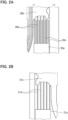
- This fixed electrode 20a has a comb teeth electrode 20c, as shown in an enlarged view in FIG. 2A .
- the movable electrode 20b has a comb teeth electrode 20d, as shown in an enlarged view in FIG. 2A .
- the comb teeth electrode 20c and the comb teeth electrode 20d are arranged so that each other's electrode branches form a line one by one in turn along the X-axis direction.
- the position of the comb teeth electrode 20c of the fixed electrode 20a does not change regardless of the movement of the outer piezoelectric actuators 6, and the position of the comb teeth electrode 20d of the movable electrode 20b changes in relation to the movement of the outer piezoelectric actuators 6.
- a capacitance component is formed between the comb teeth electrode 20c and the comb teeth electrode 20d, and its magnitude changes in accordance with the positional change of the comb teeth electrode 20d.
- a dummy comb teeth structure section 21 is a portion provided in a pair with the deflection angle detection section 20, and is configured to include a fixed electrode 21a and a movable electrode 21b.
- the fixed electrode 21a is configured integrally with the outer frame section 7.
- the movable electrode 21b has a comb teeth electrode 21d, as shown in an enlarged view of FIG. 2B .
- the fixed electrode 21a is not provided with a comb teeth electrode. Therefore, no capacitance component is formed in the dummy comb teeth structure section 21.
- the dummy comb teeth structure section 21 is provided to balance the weight between the left and right outer piezoelectric actuators 6.
- the dummy comb teeth structure section 21 and the deflection angle detection section 20 are electrically and physically separated from each other by a groove 17 provided between the respective fixed electrodes 20a and 21a, at a Si layer 53 which is an active layer (refer to FIG. 5 , which will be described later) .
- the groove 17 reaches a SiO 2 layer 52 and is electrically and physically separated from the SiO 2 layer 52.
- a detection pad 22 is connected to the fixed electrode 20a and is arranged at the lower right end in the figure.
- a detection GND pad 24 is arranged above the detection pad 22 in the figure.
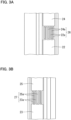
- the detection pad 22 has a comb teeth electrode 22a.
- an island-shaped dummy electrode branch 24a is provided between the respective electrode branches of the comb teeth electrode 22a.
- the dummy electrode branches 24a are not connected to the detection GND pad 24, etc., and are separated into island shapes.
- a comb teeth structure section 26 is configured by the comb teeth electrode 22a and each dummy electrode branch 24a. This comb teeth structure section 26 is a part to maintain a balance with the dummy detection section 27 and to equalize the etching area.
- the detection GND pad 24, the comb teeth electrode 22a, and the dummy electrode branch 24a are electrically and physically separated from each other by the groove 17 at the Si layer 53.
- a dummy detection pad 23 is connected to the fixed electrode 21a and is arranged at the lower left end in the figure.
- a detection GND pad 25 is arranged above the dummy detection pad 23 in the figure.
- a comb teeth electrode (first electrode) 23a is connected to the dummy detection pad 23, and a comb teeth electrode (second electrode) 25a is connected to the detection GND pad 25, and a dummy detection section (a dummy capacitance section) 27 is configured by these comb teeth electrodes 23a and 25a.
- the comb teeth electrodes 23a and 25a are electrically and physically separated from each other by the groove 17 at the Si layer 53.
- the size of the capacitance component (dummy capacitance) formed by the dummy detection section 27 is designed so that it becomes approximately equivalent to the capacitance component formed by the comb teeth electrode 20c and the comb teeth electrode 20d of the deflection angle detection section 20 in the initial state.
- the initial state refers to a state in which the outer piezoelectric actuator 6 does not fluctuate.
- the dummy detection section 27 is formed in the outer frame section 7 so that the capacitance component does not change due to the deflection angle.
- a read signal input pad 28 is arranged above the detection GND pad 25 on the left end side in the figure.
- a read signal input pad 29 is arranged above the detection GND pad 24 on the right end side in the figure.
- These read signal input pads 28 and 29 are used to input signals (read signals) used for reading the deflection angle.
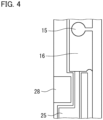
- FIG. 4 shows an enlarged plane view of the vicinity of the read signal input pad 28.
- the read signal input pad 29 has a similar structure.
- FIG. 5 is a schematic cross-sectional view corresponding to the a-a line direction shown in FIG. 1 .
- the optical scanning apparatus 1 of the present embodiment has a basic structure in which the SiO 2 (silicon dioxide) layer 52 as an etching stop layer on one side (upper side in the figure) of the Si (silicon) layer 51 as a support layer to retain the reflective section 2, etc. is provided, and in which the Si layer 53 as an active layer for forming elements is provided thereon.
- the SiO 2 (silicon dioxide) layer 52 as an etching stop layer on one side (upper side in the figure) of the Si (silicon) layer 51 as a support layer to retain the reflective section 2, etc.
- the optical scanning apparatus 1 is configured to include, in order from the bottom in the figure, a SiO 2 layer 50 as an insulating layer, the Si layer 51 as a support layer that holds the element, the SiO 2 layer (box layer) 52 as an etching stop layer, the Si layer 53 as an active layer for forming an element, a SiO 2 layer 54 as an insulating layer to insulate from the piezoelectric driving section on the upper layer side, a Pt (platinum) layer 55 as a lower electrode layer, a PZT (lead zirconate titanate) layer 56 as a piezoelectric layer, and a Pt layer 57 as an upper electrode layer.
- a SiO 2 layer 50 as an insulating layer
- the Si layer 51 as a support layer that holds the element
- the SiO 2 layer (box layer) 52 as an etching stop layer
- the Si layer 53 as an active layer for forming an element
- a SiO 2 layer 54 as an insulating layer to insulate from the
- the reflective section 2 is configured by laminating the SiO 2 layer 52, the Si layer 53, the SiO 2 layer 54, and the Pt layer 55.
- the left and right inner piezoelectric actuators 4 as a resonance driving section is configured by laminating the Si layer 53, the SiO 2 layer 54, the Pt layer 55, the PZT layer 56, and the Pt layer 57.
- each piezoelectric cantilever 13 of the left and right outer piezoelectric actuators 6 as a non-resonant driving section is configured by laminating the Si layer 53, the SiO 2 layer 54, the Pt layer 55, the PZT layer 56, and the Pt layer 57.
- the fixed electrode 20a and its comb teeth electrode 20c, and the movable electrode 20b and its comb teeth electrode 20d, which constitute the deflection angle detection section 20, are each composed of the Si layer 53. That is, the fixed electrode 20a and the movable electrode 20b are formed in the same semiconductor layer. Thereby, the Si layer 51 as a support layer can be used as a base of the element.
- the comb teeth electrode 20d of the movable electrode 20b is connected to the detection GND pad 24 through the Si layer 53 surrounded by a groove.
- the comb teeth electrode 20c of the fixed electrode 20a is integrated with the outer frame section 7.
- the comb teeth electrode 21d that constitutes the dummy comb teeth structure section 21 is composed of the Si layer 53.
- the left and right detection GND pads 24 and 25 are provided on the Si layer 53 which is stacked on the SiO 2 layer 50, the Si layer 51, and the SiO 2 layer 52. Further, each of the left and right signal reading signal input pads 28 and 29 is configured to expose the Si layer 51 on the same side as the reflective surface of the reflective section 2 by etching up to the SiO 2 layer 52 on the Si layer 51 as a support layer. This allows electrical connection to the Si layer 51 from the upper surface side of the optical scanning apparatus 1 (the side on which the laser beam is incident).
- FIG. 6 is a diagram for explaining the portion in which parasitic capacitance is generated.
- a plane view of the optical scanning apparatus 1 viewed from the back side is shown, and four portions 71, 72, 73, and 74 where parasitic capacitance is generated are shown in dark gray.
- SOI Silicon on Insulator
- the optical scanning apparatus 1 of the present embodiment uses an SOI (Silicon on Insulator) structure as shown in FIG. 5 , at a portion where the Si layer 51 which is a support layer and the Si layer 53 which is an active layer overlap, an SiO 2 layer 52 is sandwiched between each layer, thereby parasitic capacitance is formed.
- the portions 71 and 72 correspond to regions in which the driving pad 15, the driving GND pad 16, etc. are formed, respectively.
- the portions 73 and 74 correspond to regions in which the fixed electrodes 20a and 21a are formed, respectively.
- the portion 73 and the portion 74 are separated by the groove 17 described above.
- FIG. 7 is a plane view for explaining capacitance components formed in each portion of the optical scanning apparatus.
- FIG. 7 is a scaled-down version of the plane view shown in FIG. 1 , and shows locations where capacitance components are formed.
- the capacitance component corresponding to the formation region of the driving pad 15, driving GND pad 16, etc. on the upper left side in the figure is defined as C r-L .
- the capacitance component corresponding to the formation region of the driving pad 15, driving GND pad 16, etc. on the upper right side of the figure is defined as C r-R .
- the capacitance components first parasitic capacitance, second parasitic capacitance
- C s-L and C s-R are defined as C s-L and C s-R , respectively.
- the capacitance component formed at the deflection angle detection section 20 is defined as C v .
- the capacitance component (dummy capacitance) formed at the dummy detection section 27 is defined as C d .
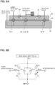
- FIG. 8A is a cross-sectional view showing the connection relationship of locations forming capacitance components in the optical scanning apparatus.
- the capacitance component C s-L is formed on a signal path leading from the Si layer 51 which is a support layer, to the dummy detection pad 23.
- the capacitance component c s-R is formed on a signal path leading from the Si layer 51 which is a support layer, to the detection pad 22.
- the capacitance component C r-L and the capacitance component C r-R are each formed on a signal path leading from the Si layer 51 which is a support layer, to the detection GND pad 24.
- the capacitance component (dummy capacitance) C d is formed in the dummy detection section 27 and is connected to the detection GND pad 24 (i.e., GND potential). Further, the capacitance component (detection capacitance) C v is formed at the deflection angle detection section 20 and is connected to the detection GND pad 24 (i.e., GND potential).
- FIG. 8B is an equivalent circuit diagram showing the connection relationship of each capacitance component.
- the capacitance component C s-L and the capacitance component C d are connected in series
- the capacitance component c s-R and the capacitance component C v are connected in series, and these are connected in parallel.
- the capacitance components C r-R and C r-L are connected in parallel to these signal paths (first signal path, second signal path), respectively.
- circuit connection lines indicated by solid lines represent connections through the Si layer 53 which is an active layer
- circuit connection lines indicated by dotted lines represent connections through the Si layer 51 which is a support layer.
- a read signal input from the read signal input pad 28 is input in parallel to each capacitance component C s-L , C s-R , C r-R , and C r-L via the Si layer 51, which is a support layer.
- the read signal passing through each capacitance component C r-R and C r-L reaches the GND potential as it is, but the read signal passing through each capacitance component C s-L and c s-R reaches the GND potential via each capacitance component C d and C v .
- a voltage signal V out1 which is divided by the capacitance component C s-L and the capacitance component C d is obtained.
- a voltage signal V out2 which is divided by the capacitance component c s-R and the capacitance component C v is obtained. Therefore, by obtaining the difference between these voltage signals V out1 and V out2 , it is possible to obtain a signal in which a common in-phase noise components are canceled. Thus, this improves the accuracy of deflection angle detection. Further, since there is no need to add a new layer as a support layer (foundation), cost increase can be suppressed.
- FIG. 9A is a waveform diagram showing an example of the read signal
- FIG. 9B is a waveform diagram showing an example of the voltage signal V out1
- FIG. 9C is a waveform diagram showing an example of the voltage signal V out2
- FIG. 9D is an enlarged waveform diagram showing an example of a differential signal between voltage signals V out1 and V out2 .
- V out 1 t V in t + N t
- the capacitance component C v and the capacitance component C d are approximately equal and the equivalent circuit is symmetrical, therefore, the voltage signal V out1 and the voltage signal V out2 are theoretically equal.
- the voltage signal V out2 increases relative to the voltage signal V out1 based on Voltage Division Rule. The opposite phenomenon occurs when the capacitance component C v increases.
- the common noise component is canceled out, and the change in voltage due to the deflection angle detection section 20 can be detected.
- the capacitance component C v changes according to the frequency of the outer piezoelectric actuator 6, which is a non-resonant driving section
- the impedance also changes periodically, and accordingly, the voltage signal V out2 also changes periodically. Since there are two points where the capacitance is maximum per period, the fluctuation cycle 90 of the differential signal is twice the driving frequency. Further, a change amount 91 of the differential signal corresponds to a change amount of the deflection angle.
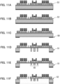
- FIGs. 10A to 10G and FIGs. 11A to 11F are process diagrams showing an example of a method for manufacturing the optical scanning apparatus.
- FIGs. 10A to 10G and FIGs. 11A to 11F are process diagrams showing an example of a method for manufacturing the optical scanning apparatus.
- an example of a method for manufacturing the optical scanning apparatus 1 will be briefly described with reference to each figure.
- a substrate in which the SiO 2 layer 50, the Si layer 51, the SiO 2 layer 52, the Si layer 53, and the SiO 2 layer 54 are stacked is prepared ( FIG. 10A ), and a Pt layer 55 is formed on one side of the SiO 2 layer 54 (the side not in contact with the Si layer 53) ( FIG. 10B ) .
- a PZT layer 56 is formed on one side of the Pt layer 55 (the side not in contact with the SiO 2 layer 54) ( FIG. 10C ), and further, a Pt layer 57 is formed on one side of the PZT layer 56 (the side not in contact with the Pt layer 55) ( FIG. 10D ).
- any known method may be used for the film formation method.
- the Pt layer 57 and the PZT layer 56 are patterned into a predetermined shape ( FIG. 10E ).
- any known method may be used for this patterning.
- a method is used in which a mask pattern is formed using a resist film (photoresist film), etching is performed, and then the resist film is peeled off (the same applies to the patterning in each subsequent step).
- the Pt layer 55 is patterned into a predetermined shape ( FIG. 10F ), and then the SiO 2 layer 54 is patterned into a predetermined shape ( FIG. 10G ). Further, the Si layer 53 is patterned into a predetermined shape ( FIG. 11A ), and then the SiO 2 layer 52 is patterned into a predetermined shape ( FIG. 11B ) .
- the SiO 2 layer 50 on the back surface side is patterned into a predetermined shape ( FIG. 11C ).
- the Si layer 51 is patterned into a predetermined shape ( FIG. 11D ), and the rib portion 60 is further formed ( FIG. 11E ) .
- the SiO 2 layer 52 is patterned into a predetermined shape ( FIG. 11F ).
- the optical scanning apparatus 1 can be applied to any electronic equipment that requires laser beam scanning.
- it can be applied to pico-projectors used in head-up displays and wearable devices.
- the present disclosure can be applied to an apparatus that changes the light distribution pattern depending on the presence of an oncoming vehicle, a preceding vehicle, a pedestrian, or various objects when irradiating light toward the front of an own vehicle.
- the present disclosure can be applied to an object detection apparatus such as LiDAR (Light Detection And Ranging).
- the present disclosure can be applied to various MEMS sensors such as an acceleration sensor, an angular velocity sensor, a pressure sensors, or a myoelectric sensor.
- FIG. 12 is a plane view from the back side of an optical scanning apparatus according to a second embodiment. Further, FIGs. 13 and 14 are partial enlarged views of the optical scanning apparatus shown in FIG. 12 , respectively.
- the overall configuration of the optical scanning apparatus 1a according to the second embodiment is the same as the optical scanning apparatus 1 according to the first embodiment described above, and only the structure of the Si layer 51 which is a support layer is different.
- the description of common features with the optical scanning apparatus 1 of the first embodiment will be omitted, and the structure of the Si layer 51 which is different, will be described in detail.
- the Si layer 51 of the optical scanning apparatus 1a is provided with a plurality of through holes 80 in a region overlapping with the Si layer 53 (that is, a portion related to the generation of parasitic capacitance), where the Si layer 53 which is an active layer that comprises capacitance component C s-L and capacitance component c s-R that are capacitance components corresponding to the formation regions of fixed electrodes 20a, 21a, etc.
- the through holes 80 are arranged in rows in the horizontal and vertical directions in the figure, but the arrangement of the through holes 80 is not limited thereto.
- the region where each through hole 80 is arranged corresponds to the above-described portions 73 and 74 (refer to FIG. 6 ).
- a plurality of through holes 81 are similarly provided in the portions 71 and 72 described above, that is, in the regions where the driving pad 15 and the driving GND pad 16 are formed.
- the size of each of the through holes 80 and 81 for example, when each is approximately square as shown in the figure, one side thereof can be approximately 50 um to 150 um.
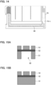
- FIGs. 15A and 15B are partial cross-sectional views of the optical scanning apparatus of the second embodiment.
- FIG. 15A is a cross-sectional view taken along line a-a shown in FIG. 13
- FIG. 15B is a cross-sectional view taken along line b-b shown in FIG. 13 .
- the through hole 80 is formed by partially removing the Si layer 51 which is a support layer, to reach the SiO 2 layer (BOX layer) 52.
- FIG. 15B at the portion where the through hole 80 does not exist, the Si layer 51 which is a support layer is not removed, and the SiO 2 layer (BOX layer) 52 is not exposed.
- each through hole 81 has a similar structure as the through hole 80.
- These through holes 80 and 81 can be formed during the process of etching the Si layer 51 (refer to FIG. 11E ) in the manufacturing process of the optical scanning apparatus 1 described in the first embodiment. Since the Si layer 51 which is a support layer also has a role of ensuring mechanical strength of the optical scanning apparatus 1a, by only partially removing the layer to form the through holes 80 and 81, a decrease in mechanical strength can be prevented.
- each through hole 80 By providing each through hole 80, it is possible to reduce the overlapping area between the Si layer 51 which is a support layer, and the Si layer 53 which is an active layer. Thereby, the values of the capacitance component C s-L and the capacitance component c s-R , which are parasitic capacitance, can be reduced. This reduces the difference between the capacitance component C v which is the capacitance component to be detected and the capacitance component C s-R . Thereby, the voltage change due to the deflection angle detection section 20 can be made greater.
- the capacitance component C v which is the capacitance component to be detected because the electrodes are formed in a direction perpendicular to the support layer or the like.
- the parasitic capacitance caused by the overlap between the Si layer 53 which is an active layer and the Si layer 51 which is a support layer is formed in a direction parallel to the support layer, etc., its value tends to increase.
- the capacitance component C v is, for example, about 1 pF, whereas the capacitance component c s-R may be about several tens of pF.
- the present disclosure is not limited to the contents of the embodiments described above, and can be implemented with various modifications within the scope of the gist of the present disclosure.
- the resonant driving section in each of the embodiments described above may be used in a non-resonant drive mode, or the non-resonance driving section may be used in a resonant drive mode.
- cases where a piezoelectric drive type actuator is used have been exemplified, but an antistatic drive type or an electromagnetic drive type actuator may be used.
- the capacitance component of the dummy detection section is formed by a comb teeth electrode, it may be formed by a parallel plate electrode.
- each of the through holes 80 and 81 in a plane view is shown as a substantially square shape as one example, it is not limited thereto, and can be formed in various shapes in a plane view, such as a circular, a triangular, or a hexagonal shape. Furthermore, the through holes 80 and 81 do not all have to be the same shape in a plane view, and may include different shapes in a plane view.
Landscapes
- Physics & Mathematics (AREA)
- General Physics & Mathematics (AREA)
- Optics & Photonics (AREA)
- Engineering & Computer Science (AREA)
- Power Engineering (AREA)
- Computer Hardware Design (AREA)
- Microelectronics & Electronic Packaging (AREA)
- Micromachines (AREA)
- Mechanical Light Control Or Optical Switches (AREA)
- Mechanical Optical Scanning Systems (AREA)
Abstract
Description
- The present disclosure relates to an optical scanning apparatus and an electronic equipment.
- There is known an optical scanning apparatus that scans incident laser beam in a two-dimensional direction. A prior art example of an optical scanning apparatus is disclosed in, for example, the following
Patent Document 1 and theNon-Patent Document 1. In such an optical scanning apparatus, it is necessary to detect the deflection angle of a movable mirror that scans the laser beam, but noise is likely to be mixed into the signal used in the process. -
- [Patent Document 1]
Japanese Patent Application Laid-Open No. 2004-245890 - [Non-patent Document 1] Hee-Moon Jeong et al., "Slow scanning electromagnetic MEMS scanner for laser display", Proc.SPIE6887, MOEMS and Maniaturized Systems VII, 688704 (8 February 2008) .
- In a specific aspect, it is an object of the present disclosure to reduce noise of the signal used to detect the deflection angle of a movable mirror.
-
- (1) An optical scanning apparatus according to one aspect of the present disclosure is an optical scanning apparatus including: (a) a mirror having a reflective surface; (b) a driving section that swings the mirror; (c) a detection section that detects the movement of the driving section by change of a capacitance; and (d) a dummy capacitance section that generates a dummy capacitance that is approximately equivalent to the capacitance in an initial state of the detection section; (e) where the detection section has a movable electrode whose position changes in relation to the movement of the driving section and a fixed electrode whose position does not change in relation to the movement of the driving section, and is configured such that the capacitance is generated between the movable electrode and the fixed electrode, (f) where the dummy capacitance section is configured to include a first electrode and a second electrode, and is configured to generate the dummy capacitance between the first electrode and the second electrode, (g) where the movable electrode, the fixed electrode, the first electrode, and the second electrode are provided in an active layer formed in the same semiconductor layer, and are each separated, and where the active layer is arranged to face a support layer which is a common semiconductor layer, with an insulating layer in between, (h) where a first parasitic capacitance that occurs between the active layer provided with the fixed electrode and the supporting layer, and a second parasitic capacitance that occurs between the active layer provided with the first electrode and the supporting layer, are approximately equivalent, and (i) where the capacitance of the detection section and the first parasitic capacitance are connected in series to form a first signal path, and the dummy capacitance and the second parasitic capacitance are connected in series to form a second signal path.
- (2) An electronic equipment according to one aspect of the present disclosure is an electronic equipment including the optical scanning apparatus according to the above-described (1) .
- According to the above configurations, it is possible to reduce noise of the signal used to detect the deflection angle of a movable mirror.
-
-
FIG. 1 is a plane view showing the configuration of an optical scanning apparatus (optical deflector) according to a first embodiment. -
FIG. 2A is an enlarged view of a deflection angle detection section. -
FIG. 2B is an enlarged view of a dummy comb teeth structure section. -
FIG. 3A is an enlarged view of a detection pad. -
FIG. 3B is an enlarged view of a dummy detection pad. -
FIG. 4 is an enlarged plane view of the vicinity of a read signal input pad. -
FIG. 5 is a schematic cross-sectional view corresponding to the a-a line direction shown inFIG. 1 . -
FIG. 6 is a diagram for explaining the portion in which parasitic capacitance is generated. -
FIG. 7 is a plane view for explaining capacitance components formed in each portion of the optical scanning apparatus. -
FIG. 8A is a cross-sectional view showing the connection relationship of locations forming capacitance components in the optical scanning apparatus. -
FIG. 8B is an equivalent circuit diagram showing the connection relationship of each capacitance component. -
FIG. 9A is a waveform diagram showing an example of a read signal. -
FIG. 9B is a waveform diagram showing an example of a voltage signal Vout1. -
FIG. 9C is a waveform diagram showing an example of a voltage signal Vout2. -
FIG. 9D is an enlarged waveform diagram showing an example of a differential signal between voltage signals Vout1 and Vout2. -
FIGs. 10A to 10G are process diagrams showing an example of a method for manufacturing an optical scanning apparatus. -
FIGs. 11A to 11F are process diagrams showing an example of a method for manufacturing an optical scanning apparatus. -
FIG. 12 is a plane view showing the configuration of an optical scanning apparatus according to a second embodiment. -
FIG. 13 is a partial enlarged view of the optical scanning apparatus shown inFIG. 12 . -
FIG. 14 is a partial enlarged view of the optical scanning apparatus shown inFIG. 12 . -
FIGs. 15A and 15B are partial cross-sectional views of the optical scanning apparatus of a second embodiment. -
FIG. 1 is a plane view showing the configuration of an optical scanning apparatus (optical deflector) 1 according to a first embodiment. In the present embodiment, the surface into which the laser beam to be scanned enters is defined as the front surface, and the surface on the opposite side thereof is defined as the back surface.FIG. 1 shows a plane view seen from the front surface side. As illustrated, theoptical scanning apparatus 1 of the present embodiment has an almost bilaterally symmetrical structure in a plane view. - The
optical scanning apparatus 1 is configured to include a reflecting section (mirror) 2, atorsion bar 3, innerpiezoelectric actuators 4, aninner frame section 5, outer piezoelectric actuators (drive sections) 6, and an outer frame section (frame) 7 as a main component. The horizontal direction in the figure is defined as the X axis, the vertical direction as the Y axis, and the thickness direction of the optical scanning apparatus 1 (direction perpendicular to the diagram sheet surface) as the Z axis. - The reflecting
section 2 is a movable mirror having a substantially circular reflecting surface in a plane view, and is configured to be swingable around the Y-axis and the X-axis by the innerpiezoelectric actuators 4 and the outerpiezoelectric actuators 6. By reflecting a laser beam by such reflectingsection 2, the laser beam incident on the reflectingsection 2 can be scanned in a two-dimensional direction. - The
torsion bar 3 is provided, in a plane view, above and below the reflectingsection 2. Thetorsion bar 3 extends along the Y-axis direction from the reflectingsection 2 and is coupled to the inner periphery of theinner frame section 5. Further, thetorsion bar 3 is coupled to the upper and lower ends of the left and right innerpiezoelectric actuators 4. - The inner
piezoelectric actuators 4 and the outerpiezoelectric actuators 6 are provided one each on the left and right sides of the reflectingsection 2 in a plane view. - The inner
piezoelectric actuators 4 are coupled to each other, and have an overall shape close to an ellipse that extends along the Y-axis in a plane view. - The outer
piezoelectric actuators 6 are interposed between theinner frame section 5 and theouter frame section 7. Each of the outerpiezoelectric actuators 6 is configured to include a plurality ofpiezoelectric cantilevers 13. Among thepiezoelectric cantilevers 13, the one closest to the reflectingsection 2 and the one farthest from the reflectingsection 2 have shorter lengths in the Y-axis direction than the otherpiezoelectric cantilevers 13. Further, eachpiezoelectric cantilever 13 has a width in the X-axis direction that becomes relatively small as it is located closer to the reflectingsection 2. - The
inner frame section 5 surrounds the reflectingsection 2 and thetorsion bar 3. Theinner frame section 5 has an overall shape close to an ellipse that extends along the Y-axis in a plane view. - A
driving pad 15 and a drivingGND pad 16 are respectively provided on the left and right upper sides of theouter frame section 7 in a plane view. Thedriving pad 15 has a plurality of circular portions in a plane view. Thedriving pad 15 and the drivingGND pad 16 are electrically/physically connected to the outside via bonding wires (not shown) when theoptical scanning apparatus 1 is packaged. - The
driving pad 15 and the drivingGND pad 16 on the right side in the figure are used to supply a drive voltage to the innerpiezoelectric actuator 4 on the right side in the figure. Similarly, thedriving pad 15 and the drivingGND pad 16 on the left side in the figure are used to supply a drive voltage to the innerpiezoelectric actuator 4 on the left side in the figure. Each innerpiezoelectric actuator 4 is interposed between thetorsion bar 3 and theinner frame section 5, and oscillates the reflectingsection 2 around the Y axis at a first frequency by twisting thetorsion bar 3. Resonance is used for this oscillation. The first frequency is, for example, 15kHz to 25kHz. - Each outer
piezoelectric actuator 6 is supplied with a drive voltage of a second frequency via thedriving pad 15 and the drivingGND pad 16. Thereby, the reflectingsection 2 oscillates around the X-axis at the second frequency. Resonance is not used for the oscillation around the X-axis. The second frequency is lower than the first frequency described above, and is set to, for example, 60 Hz. - Laser beam that enters the reflecting
section 2 from a light source (not shown) is reflected in a direction according to the swing angle (deflection angle) of the reflectingsection 2 around the X-axis and the Y-axis. The reflecting direction (deflecting direction) changes moment by moment according to changes in the swing angle of thereflection section 2. Thereby, the laser beam reflected by thereflection section 2 is scanned around the Y-axis at the first frequency and scanned around the X-axis at the second frequency. - A deflection angle detection section (a detection section) 20 is for detecting the deflection angle of the
reflection section 2 by detecting the movement accompanying non-resonant vibration by the outerpiezoelectric actuators 6 as a change of a capacitance, and is configured to include a fixedelectrode 20a and amovable electrode 20b. The fixedelectrode 20a is configured integrally with theouter frame section 7. Thisfixed electrode 20a has acomb teeth electrode 20c, as shown in an enlarged view inFIG. 2A . Themovable electrode 20b has acomb teeth electrode 20d, as shown in an enlarged view inFIG. 2A . Thecomb teeth electrode 20c and thecomb teeth electrode 20d are arranged so that each other's electrode branches form a line one by one in turn along the X-axis direction. The position of thecomb teeth electrode 20c of the fixedelectrode 20a does not change regardless of the movement of the outerpiezoelectric actuators 6, and the position of thecomb teeth electrode 20d of themovable electrode 20b changes in relation to the movement of the outerpiezoelectric actuators 6. A capacitance component (capacitance) is formed between thecomb teeth electrode 20c and thecomb teeth electrode 20d, and its magnitude changes in accordance with the positional change of thecomb teeth electrode 20d. - A dummy comb
teeth structure section 21 is a portion provided in a pair with the deflectionangle detection section 20, and is configured to include a fixedelectrode 21a and amovable electrode 21b. The fixedelectrode 21a is configured integrally with theouter frame section 7. Themovable electrode 21b has acomb teeth electrode 21d, as shown in an enlarged view ofFIG. 2B . In the dummy combteeth structure section 21, the fixedelectrode 21a is not provided with a comb teeth electrode. Therefore, no capacitance component is formed in the dummy combteeth structure section 21. The dummy combteeth structure section 21 is provided to balance the weight between the left and right outerpiezoelectric actuators 6. - The dummy comb
teeth structure section 21 and the deflectionangle detection section 20 are electrically and physically separated from each other by agroove 17 provided between the respectivefixed electrodes Si layer 53 which is an active layer (refer toFIG. 5 , which will be described later) . Thegroove 17 reaches a SiO2 layer 52 and is electrically and physically separated from the SiO2 layer 52. - A
detection pad 22 is connected to the fixedelectrode 20a and is arranged at the lower right end in the figure. Adetection GND pad 24 is arranged above thedetection pad 22 in the figure. As shown in an enlarged view inFIG. 3A , thedetection pad 22 has acomb teeth electrode 22a. Further, an island-shapeddummy electrode branch 24a is provided between the respective electrode branches of thecomb teeth electrode 22a. Thedummy electrode branches 24a are not connected to thedetection GND pad 24, etc., and are separated into island shapes. A combteeth structure section 26 is configured by thecomb teeth electrode 22a and eachdummy electrode branch 24a. This combteeth structure section 26 is a part to maintain a balance with thedummy detection section 27 and to equalize the etching area. Thedetection GND pad 24, thecomb teeth electrode 22a, and thedummy electrode branch 24a are electrically and physically separated from each other by thegroove 17 at theSi layer 53. - A
dummy detection pad 23 is connected to the fixedelectrode 21a and is arranged at the lower left end in the figure. Adetection GND pad 25 is arranged above thedummy detection pad 23 in the figure. As shown in an enlarged view inFIG. 3B , a comb teeth electrode (first electrode) 23a is connected to thedummy detection pad 23, and a comb teeth electrode (second electrode) 25a is connected to thedetection GND pad 25, and a dummy detection section (a dummy capacitance section) 27 is configured by thesecomb teeth electrodes comb teeth electrodes groove 17 at theSi layer 53. The size of the capacitance component (dummy capacitance) formed by thedummy detection section 27 is designed so that it becomes approximately equivalent to the capacitance component formed by thecomb teeth electrode 20c and thecomb teeth electrode 20d of the deflectionangle detection section 20 in the initial state. Here, note that the initial state refers to a state in which the outerpiezoelectric actuator 6 does not fluctuate. Thedummy detection section 27 is formed in theouter frame section 7 so that the capacitance component does not change due to the deflection angle. - A read
signal input pad 28 is arranged above thedetection GND pad 25 on the left end side in the figure. A readsignal input pad 29 is arranged above thedetection GND pad 24 on the right end side in the figure. These readsignal input pads FIG. 4 shows an enlarged plane view of the vicinity of the readsignal input pad 28. Here, note that although an enlarged view is omitted, the readsignal input pad 29 has a similar structure. -
FIG. 5 is a schematic cross-sectional view corresponding to the a-a line direction shown inFIG. 1 . Here, note that inFIG. 5 , the structure of theoptical scanning apparatus 1 is illustrated in a modified manner in order to make it easier to understand the laminated structure and the configuration of each section. Theoptical scanning apparatus 1 of the present embodiment has a basic structure in which the SiO2 (silicon dioxide)layer 52 as an etching stop layer on one side (upper side in the figure) of the Si (silicon)layer 51 as a support layer to retain thereflective section 2, etc. is provided, and in which theSi layer 53 as an active layer for forming elements is provided thereon. - Specifically, the
optical scanning apparatus 1 is configured to include, in order from the bottom in the figure, a SiO2 layer 50 as an insulating layer, theSi layer 51 as a support layer that holds the element, the SiO2 layer (box layer) 52 as an etching stop layer, theSi layer 53 as an active layer for forming an element, a SiO2 layer 54 as an insulating layer to insulate from the piezoelectric driving section on the upper layer side, a Pt (platinum)layer 55 as a lower electrode layer, a PZT (lead zirconate titanate)layer 56 as a piezoelectric layer, and aPt layer 57 as an upper electrode layer. Each of these layers is patterned into a predetermined shape. - As shown in the figure, based on a reinforcing
rib layer 60 formed by etching theSi layer 51 halfway, thereflective section 2 is configured by laminating the SiO2 layer 52, theSi layer 53, the SiO2 layer 54, and thePt layer 55. - The left and right inner
piezoelectric actuators 4 as a resonance driving section is configured by laminating theSi layer 53, the SiO2 layer 54, thePt layer 55, thePZT layer 56, and thePt layer 57. Similarly, eachpiezoelectric cantilever 13 of the left and right outerpiezoelectric actuators 6 as a non-resonant driving section is configured by laminating theSi layer 53, the SiO2 layer 54, thePt layer 55, thePZT layer 56, and thePt layer 57. - The fixed
electrode 20a and itscomb teeth electrode 20c, and themovable electrode 20b and itscomb teeth electrode 20d, which constitute the deflectionangle detection section 20, are each composed of theSi layer 53. That is, the fixedelectrode 20a and themovable electrode 20b are formed in the same semiconductor layer. Thereby, theSi layer 51 as a support layer can be used as a base of the element. Thecomb teeth electrode 20d of themovable electrode 20b is connected to thedetection GND pad 24 through theSi layer 53 surrounded by a groove. Thecomb teeth electrode 20c of the fixedelectrode 20a is integrated with theouter frame section 7. - Similarly, the
comb teeth electrode 21d that constitutes the dummy combteeth structure section 21 is composed of theSi layer 53. - The left and right
detection GND pads Si layer 53 which is stacked on the SiO2 layer 50, theSi layer 51, and the SiO2 layer 52. Further, each of the left and right signal readingsignal input pads Si layer 51 on the same side as the reflective surface of thereflective section 2 by etching up to the SiO2 layer 52 on theSi layer 51 as a support layer. This allows electrical connection to theSi layer 51 from the upper surface side of the optical scanning apparatus 1 (the side on which the laser beam is incident). -
FIG. 6 is a diagram for explaining the portion in which parasitic capacitance is generated. InFIG. 6 , a plane view of theoptical scanning apparatus 1 viewed from the back side is shown, and fourportions optical scanning apparatus 1 of the present embodiment uses an SOI (Silicon on Insulator) structure as shown inFIG. 5 , at a portion where theSi layer 51 which is a support layer and theSi layer 53 which is an active layer overlap, an SiO2 layer 52 is sandwiched between each layer, thereby parasitic capacitance is formed. Theportions driving pad 15, the drivingGND pad 16, etc. are formed, respectively. Theportions electrodes portion 73 and theportion 74 are separated by thegroove 17 described above. -
FIG. 7 is a plane view for explaining capacitance components formed in each portion of the optical scanning apparatus.FIG. 7 is a scaled-down version of the plane view shown inFIG. 1 , and shows locations where capacitance components are formed. The capacitance component corresponding to the formation region of thedriving pad 15, drivingGND pad 16, etc. on the upper left side in the figure is defined as Cr-L. The capacitance component corresponding to the formation region of thedriving pad 15, drivingGND pad 16, etc. on the upper right side of the figure is defined as Cr-R. Further, the capacitance components (first parasitic capacitance, second parasitic capacitance) corresponding to the formation regions of fixedelectrodes dummy detection section 27 is defined as Cd. -
FIG. 8A is a cross-sectional view showing the connection relationship of locations forming capacitance components in the optical scanning apparatus. Here, for ease of understanding, portions related to capacitance components are shown in a modified manner. As shown in the figure, the capacitance component Cs-L is formed on a signal path leading from theSi layer 51 which is a support layer, to thedummy detection pad 23. The capacitance component cs-R is formed on a signal path leading from theSi layer 51 which is a support layer, to thedetection pad 22. The capacitance component Cr-L and the capacitance component Cr-R are each formed on a signal path leading from theSi layer 51 which is a support layer, to thedetection GND pad 24. Further, the capacitance component (dummy capacitance) Cd is formed in thedummy detection section 27 and is connected to the detection GND pad 24 (i.e., GND potential). Further, the capacitance component (detection capacitance) Cv is formed at the deflectionangle detection section 20 and is connected to the detection GND pad 24 (i.e., GND potential). -
FIG. 8B is an equivalent circuit diagram showing the connection relationship of each capacitance component. As shown, the capacitance component Cs-L and the capacitance component Cd are connected in series, the capacitance component cs-R and the capacitance component Cv are connected in series, and these are connected in parallel. Further, the capacitance components Cr-R and Cr-L are connected in parallel to these signal paths (first signal path, second signal path), respectively. Here, note that in the figure, circuit connection lines indicated by solid lines represent connections through theSi layer 53 which is an active layer, and circuit connection lines indicated by dotted lines represent connections through theSi layer 51 which is a support layer. - A read signal input from the read
signal input pad 28 is input in parallel to each capacitance component Cs-L, Cs-R, Cr-R, and Cr-L via theSi layer 51, which is a support layer. The read signal passing through each capacitance component Cr-R and Cr-L reaches the GND potential as it is, but the read signal passing through each capacitance component Cs-L and cs-R reaches the GND potential via each capacitance component Cd and Cv. - From the
dummy detection pad 23, a voltage signal Vout1 which is divided by the capacitance component Cs-L and the capacitance component Cd, is obtained. From thedetection pad 22, a voltage signal Vout2 which is divided by the capacitance component cs-R and the capacitance component Cv, is obtained. Therefore, by obtaining the difference between these voltage signals Vout1 and Vout2, it is possible to obtain a signal in which a common in-phase noise components are canceled. Thus, this improves the accuracy of deflection angle detection. Further, since there is no need to add a new layer as a support layer (foundation), cost increase can be suppressed. -
FIG. 9A is a waveform diagram showing an example of the read signal,FIG. 9B is a waveform diagram showing an example of the voltage signal Vout1,FIG. 9C is a waveform diagram showing an example of the voltage signal Vout2, andFIG. 9D is an enlarged waveform diagram showing an example of a differential signal between voltage signals Vout1 and Vout2. Here, when defining a read signal which is an input voltage at a certain time "t" as Vin(t), noise as N(t), and a differential signal between the voltage signals Vout1(t) and Vout2(t) as v(t), these parameters can be expressed as follows.


- When the deflection
angle detection section 20 is at the initial position, the capacitance component Cv and the capacitance component Cd are approximately equal and the equivalent circuit is symmetrical, therefore, the voltage signal Vout1 and the voltage signal Vout2 are theoretically equal. Considering a case where the deflectionangle detection section 20 operates and the capacitance component Cv decreases, that is, a case where the impedance increases, the voltage signal Vout2 increases relative to the voltage signal Vout1 based on Voltage Division Rule. The opposite phenomenon occurs when the capacitance component Cv increases. Therefore, by obtaining the difference between the voltage signal Vout1 and the voltage signal Vout2, the common noise component is canceled out, and the change in voltage due to the deflectionangle detection section 20 can be detected. In detail, as shown inFIG. 9D , since the capacitance component Cv changes according to the frequency of the outerpiezoelectric actuator 6, which is a non-resonant driving section, the impedance also changes periodically, and accordingly, the voltage signal Vout2 also changes periodically. Since there are two points where the capacitance is maximum per period, thefluctuation cycle 90 of the differential signal is twice the driving frequency. Further, achange amount 91 of the differential signal corresponds to a change amount of the deflection angle. -
FIGs. 10A to 10G andFIGs. 11A to 11F are process diagrams showing an example of a method for manufacturing the optical scanning apparatus. Hereinafter, an example of a method for manufacturing theoptical scanning apparatus 1 will be briefly described with reference to each figure. - First, a substrate in which the SiO2 layer 50, the
Si layer 51, the SiO2 layer 52, theSi layer 53, and the SiO2 layer 54 are stacked is prepared (FIG. 10A ), and aPt layer 55 is formed on one side of the SiO2 layer 54 (the side not in contact with the Si layer 53) (FIG. 10B ) . Next, aPZT layer 56 is formed on one side of the Pt layer 55 (the side not in contact with the SiO2 layer 54) (FIG. 10C ), and further, aPt layer 57 is formed on one side of the PZT layer 56 (the side not in contact with the Pt layer 55) (FIG. 10D ). Here, note that any known method may be used for the film formation method. - Next, the
Pt layer 57 and thePZT layer 56 are patterned into a predetermined shape (FIG. 10E ). Here, any known method may be used for this patterning. As an example, in the present embodiment, a method is used in which a mask pattern is formed using a resist film (photoresist film), etching is performed, and then the resist film is peeled off (the same applies to the patterning in each subsequent step). - Next, the
Pt layer 55 is patterned into a predetermined shape (FIG. 10F ), and then the SiO2 layer 54 is patterned into a predetermined shape (FIG. 10G ). Further, theSi layer 53 is patterned into a predetermined shape (FIG. 11A ), and then the SiO2 layer 52 is patterned into a predetermined shape (FIG. 11B ) . - Next, the SiO2 layer 50 on the back surface side is patterned into a predetermined shape (
FIG. 11C ). Then theSi layer 51 is patterned into a predetermined shape (FIG. 11D ), and therib portion 60 is further formed (FIG. 11E ) . Thereafter, the SiO2 layer 52 is patterned into a predetermined shape (FIG. 11F ). Through the above steps, theoptical scanning apparatus 1 according to the embodiment described above is completed. - According to the first embodiment as described above, it is possible to reduce noise of the signal used to detect the deflection angle of the movable mirror.
- The
optical scanning apparatus 1 according to the first embodiment described above can be applied to any electronic equipment that requires laser beam scanning. For example, it can be applied to pico-projectors used in head-up displays and wearable devices. Further, the present disclosure can be applied to an apparatus that changes the light distribution pattern depending on the presence of an oncoming vehicle, a preceding vehicle, a pedestrian, or various objects when irradiating light toward the front of an own vehicle. Alternatively, the present disclosure can be applied to an object detection apparatus such as LiDAR (Light Detection And Ranging). Further, the present disclosure can be applied to various MEMS sensors such as an acceleration sensor, an angular velocity sensor, a pressure sensors, or a myoelectric sensor. -
FIG. 12 is a plane view from the back side of an optical scanning apparatus according to a second embodiment. Further,FIGs. 13 and14 are partial enlarged views of the optical scanning apparatus shown inFIG. 12 , respectively. Here, note that the overall configuration of theoptical scanning apparatus 1a according to the second embodiment is the same as theoptical scanning apparatus 1 according to the first embodiment described above, and only the structure of theSi layer 51 which is a support layer is different. Hereinafter, regarding theoptical scanning apparatus 1a according to the second embodiment, the description of common features with theoptical scanning apparatus 1 of the first embodiment will be omitted, and the structure of theSi layer 51 which is different, will be described in detail. - As shown in the figure, the
Si layer 51 of theoptical scanning apparatus 1a is provided with a plurality of throughholes 80 in a region overlapping with the Si layer 53 (that is, a portion related to the generation of parasitic capacitance), where theSi layer 53 which is an active layer that comprises capacitance component Cs-L and capacitance component cs-R that are capacitance components corresponding to the formation regions of fixedelectrodes holes 80 are arranged in rows in the horizontal and vertical directions in the figure, but the arrangement of the throughholes 80 is not limited thereto. The region where each throughhole 80 is arranged corresponds to the above-describedportions 73 and 74 (refer toFIG. 6 ). Further, a plurality of throughholes 81 are similarly provided in theportions driving pad 15 and the drivingGND pad 16 are formed. With regard to the size of each of the throughholes -
FIGs. 15A and 15B are partial cross-sectional views of the optical scanning apparatus of the second embodiment.FIG. 15A is a cross-sectional view taken along line a-a shown inFIG. 13 , andFIG. 15B is a cross-sectional view taken along line b-b shown inFIG. 13 . As shown inFIG. 15A , the throughhole 80 is formed by partially removing theSi layer 51 which is a support layer, to reach the SiO2 layer (BOX layer) 52. On the other hand, as shown inFIG. 15B , at the portion where the throughhole 80 does not exist, theSi layer 51 which is a support layer is not removed, and the SiO2 layer (BOX layer) 52 is not exposed. Here, although not shown, each throughhole 81 has a similar structure as the throughhole 80. These throughholes FIG. 11E ) in the manufacturing process of theoptical scanning apparatus 1 described in the first embodiment. Since theSi layer 51 which is a support layer also has a role of ensuring mechanical strength of theoptical scanning apparatus 1a, by only partially removing the layer to form the throughholes - By providing each through
hole 80, it is possible to reduce the overlapping area between theSi layer 51 which is a support layer, and theSi layer 53 which is an active layer. Thereby, the values of the capacitance component Cs-L and the capacitance component cs-R , which are parasitic capacitance, can be reduced. This reduces the difference between the capacitance component Cv which is the capacitance component to be detected and the capacitance component Cs-R. Thereby, the voltage change due to the deflectionangle detection section 20 can be made greater. - In detail, it is difficult to increase the value of the capacitance component Cv which is the capacitance component to be detected because the electrodes are formed in a direction perpendicular to the support layer or the like. On the other hand, since the parasitic capacitance caused by the overlap between the
Si layer 53 which is an active layer and theSi layer 51 which is a support layer is formed in a direction parallel to the support layer, etc., its value tends to increase. When through holes 80 are not provided, the capacitance component Cv is, for example, about 1 pF, whereas the capacitance component cs-R may be about several tens of pF. In principle, when the ratio of the capacitance component Cv to the capacitance component cs-R (Cs-R/Cv) is around 1, amount of voltage change due to the deflectionangle detection section 20 reaches its maximum value . As the capacitance component cs-R decreases, the value of Cs-R/Cv approaches 1, thereby the amount of voltage change can be made greater. - Here, note that the present disclosure is not limited to the contents of the embodiments described above, and can be implemented with various modifications within the scope of the gist of the present disclosure. For example, the resonant driving section in each of the embodiments described above may be used in a non-resonant drive mode, or the non-resonance driving section may be used in a resonant drive mode. Further, in each of the above-described embodiments, cases where a piezoelectric drive type actuator is used have been exemplified, but an antistatic drive type or an electromagnetic drive type actuator may be used. Further, although the capacitance component of the dummy detection section is formed by a comb teeth electrode, it may be formed by a parallel plate electrode. Further, in each of the embodiments described above, two read signal input pads have been provided, but one or three or more pads may be provided instead. Further, the read signal may be applied from the opposite side (movable electrode side). Further, although the shape of each of the through
holes holes -
- 1:
- Optical scanning apparatus
- 2:
- Reflecting section (Movable mirror)
- 3:
- Torsion bar
- 4:
- Inner piezoelectric actuator
- 5:
- Inner frame section
- 6:
- Outer piezoelectric actuator
- 7:
- Outer frame section (frame)
- 13:
- Piezoelectric Cantilever
- 15:
- Driving pad
- 16:
- Driving GND pad
- 17:
- Groove
- 20:
- Deflection angle detection section
- 20a:
- Fixed electrode
- 20b:
- Movable electrode
- 20c, 20d:
- Comb teeth electrode
- 21:
- Dummy comb teeth structure section
- 21a:
- Fixed electrode
- 21b:
- Movable electrode
- 22:
- Detection pad
- 22a:
- Comb teeth electrode
- 23:
- Dummy detection pad
- 23a:
- Comb teeth electrode
- 24:
- Detection GND pad
- 24a:
- Dummy electrode branch
- 25:
- Detection GND pad
- 25a:
- Comb teeth electrode
- 26:
- Comb teeth structure section
- 27:
- Dummy detection section
- 28, 29:
- Read signal input pad
- 50:
- SiO2 layer
- 51:
- Si layer
- 52:
- SiO2 layer (Box layer)
- 53:
- Si layer
- 54:
- SiO2 layer
- 55:
- Pt layer
- 56:
- PZT (lead zirconate titanate) layer
- 57:
- Pt layer
- 80, 81:
- Through hole
Claims (9)
- An optical scanning apparatus comprising:a mirror having a reflective surface;a driving section that swings the mirror;a detection section that detects the movement of the driving section by change of a capacitance; anda dummy capacitance section that generates a dummy capacitance that is approximately equivalent to the capacitance in an initial state of the detection section;wherein the detection section has a movable electrode whose position changes in relation to the movement of the driving section and a fixed electrode whose position does not change in relation to the movement of the driving section, and is configured such that the capacitance is generated between the movable electrode and the fixed electrode,wherein the dummy capacitance section is configured to include a first electrode and a second electrode, and is configured to generate the dummy capacitance between the first electrode and the second electrode,wherein the movable electrode, the fixed electrode, the first electrode, and the second electrode are provided in an active layer formed in the same semiconductor layer, and are each separated,wherein the active layer is arranged to face a support layer which is a common semiconductor layer, with an insulating layer in between,wherein a first parasitic capacitance that occurs between the active layer provided with the fixed electrode and the supporting layer, and a second parasitic capacitance that occurs between the active layer provided with the first electrode and the supporting layer, are approximately equivalent, andwherein the capacitance of the detection section and the first parasitic capacitance are connected in series to form a first signal path, and the dummy capacitance and the second parasitic capacitance are connected in series to form a second signal path.
- The optical scanning apparatus according to claim 1,wherein the first signal path and the second signal path are connected in parallel, andwherein the active layer is configured to include a detection pad that can obtain a partial voltage between the capacitance of the detection section and the first parasitic capacitance, and a dummy detection pad that can obtain a partial voltage between the dummy capacitance and the second parasitic capacitance.
- The optical scanning apparatus according to claim 1 or claim 2,
wherein the support layer has a read signal input pad configured to be exposed on the same side as the reflective surface of the mirror. - The optical scanning apparatus according to any one of claims 1 to 3,
wherein the area of the fixed electrode in a plane view and the area of the first electrode in a plane view are approximately equal. - The optical scanning apparatus according to any one of claims 1 to 4,
wherein the movable electrode and the fixed electrode each have a comb teeth electrode, and capacitance is generated between these comb teeth electrodes. - The optical scanning apparatus according to any one of claims 1 to 5,
wherein the first electrode and the second electrode each have a comb teeth electrode, and dummy capacitance is generated between these comb teeth electrodes. - The optical scanning apparatus according to any one of claims 1 to 6,
wherein a read signal is input to the support layer, and a deflection angle of the mirror is determined based on a difference between a partial voltage between the capacitance of the detection section and the first parasitic capacitance, and the partial voltage between the dummy capacitance and the second parasitic capacitance. - The optical scanning apparatus according to any one of claims 1 to 7,
wherein the support layer has a plurality of through holes each reaching the insulating layer at a portion related to the generation of each of the first parasitic capacitance and the second parasitic capacitance. - An electronic equipment comprising the optical scanning apparatus according to any one of claims 1 to 8.
Applications Claiming Priority (2)
| Application Number | Priority Date | Filing Date | Title |
|---|---|---|---|
| JP2021097540 | 2021-06-10 | ||
| PCT/JP2022/022091 WO2022259912A1 (en) | 2021-06-10 | 2022-05-31 | Optical scanning device and electronic apparatus |
Publications (3)
| Publication Number | Publication Date |
|---|---|
| EP4336240A1 true EP4336240A1 (en) | 2024-03-13 |
| EP4336240A4 EP4336240A4 (en) | 2024-11-20 |
| EP4336240B1 EP4336240B1 (en) | 2025-07-30 |
Family
ID=84424968
Family Applications (1)
| Application Number | Title | Priority Date | Filing Date |
|---|---|---|---|
| EP22820094.5A Active EP4336240B1 (en) | 2021-06-10 | 2022-05-31 | Optical scanning device and electronic apparatus |
Country Status (5)
| Country | Link |
|---|---|
| US (1) | US20240280384A1 (en) |
| EP (1) | EP4336240B1 (en) |
| JP (1) | JP7822376B2 (en) |
| CN (1) | CN117413214A (en) |
| WO (1) | WO2022259912A1 (en) |
Families Citing this family (1)
| Publication number | Priority date | Publication date | Assignee | Title |
|---|---|---|---|---|
| JP2025030740A (en) * | 2023-08-24 | 2025-03-07 | スタンレー電気株式会社 | Optical deflectors, electronic devices |
Family Cites Families (13)
| Publication number | Priority date | Publication date | Assignee | Title |
|---|---|---|---|---|
| JP3011144B2 (en) * | 1997-07-31 | 2000-02-21 | 日本電気株式会社 | Optical scanner and its driving method |
| US7185542B2 (en) * | 2001-12-06 | 2007-03-06 | Microfabrica Inc. | Complex microdevices and apparatus and methods for fabricating such devices |
| JP2004245890A (en) | 2003-02-10 | 2004-09-02 | Denso Corp | Optical scanning device |
| JP2006201519A (en) * | 2005-01-20 | 2006-08-03 | Ricoh Co Ltd | Optical scanner and image forming apparatus |
| JP2011058819A (en) * | 2009-09-07 | 2011-03-24 | Seiko Epson Corp | Mems sensor and method for manufacturing the same |
| JP6319758B2 (en) * | 2013-02-28 | 2018-05-09 | デクセリアルズ株式会社 | Capacitance device, resonance circuit, and electronic equipment |
| EP3059838B1 (en) * | 2013-10-17 | 2019-07-03 | Mitsubishi Electric Corporation | Noise filter |
| JP2016059191A (en) * | 2014-09-11 | 2016-04-21 | ソニー株式会社 | Electrostatic device |
| JP6459392B2 (en) * | 2014-10-28 | 2019-01-30 | ミツミ電機株式会社 | Optical scanning device |
| JP2017020897A (en) * | 2015-07-10 | 2017-01-26 | セイコーエプソン株式会社 | Physical quantity sensor, electronic apparatus and mobile body |
| JP2017058418A (en) * | 2015-09-14 | 2017-03-23 | 富士電機株式会社 | Optical scanning device and endoscope |
| US11789253B2 (en) * | 2020-09-01 | 2023-10-17 | Beijing Voyager Technology Co., Ltd. | Capacitance sensing in a MEMS mirror structure |
| US11835710B2 (en) * | 2020-12-15 | 2023-12-05 | Infineon Technologies Ag | Method of mode coupling detection and damping and usage for electrostatic MEMS mirrors |
-
2022
- 2022-05-31 EP EP22820094.5A patent/EP4336240B1/en active Active
- 2022-05-31 US US18/567,476 patent/US20240280384A1/en not_active Abandoned
- 2022-05-31 WO PCT/JP2022/022091 patent/WO2022259912A1/en not_active Ceased
- 2022-05-31 CN CN202280039326.8A patent/CN117413214A/en active Pending
- 2022-05-31 JP JP2023527630A patent/JP7822376B2/en active Active
Also Published As
| Publication number | Publication date |
|---|---|
| EP4336240A4 (en) | 2024-11-20 |
| JPWO2022259912A1 (en) | 2022-12-15 |
| WO2022259912A1 (en) | 2022-12-15 |
| CN117413214A (en) | 2024-01-16 |
| EP4336240B1 (en) | 2025-07-30 |
| US20240280384A1 (en) | 2024-08-22 |
| JP7822376B2 (en) | 2026-03-02 |
Similar Documents
| Publication | Publication Date | Title |
|---|---|---|
| JP5486312B2 (en) | Micromirror actuator having encapsulation capability and method of manufacturing the same | |
| US9097897B2 (en) | Optical deflector including narrow piezoelectric sensor element between torsion bar and piezoelectric actuator | |
| US9323048B2 (en) | Optical deflector including meander-type piezoelectric actuators coupled by crossing bars therebetween | |
| JP6789438B2 (en) | Optical scanning device and its control method | |
| JP2014215534A (en) | Optical scanner | |
| US20160116733A1 (en) | Optical scanner apparatus | |
| EP3650910B1 (en) | Optical device | |
| CN103097937A (en) | Oscillation mirror element | |
| JP5056633B2 (en) | Micro oscillating device, micro oscillating device array, and optical switching device | |
| EP4336240B1 (en) | Optical scanning device and electronic apparatus | |
| US9436000B2 (en) | Optical deflector including meander-type piezoelectric actuators and ill-balanced mirror structure | |
| JP2022143323A (en) | Movable device, image projector, head-up display, laser head lamp, head-mount display, distance measuring device, and mobile body | |
| JPH11242180A (en) | Optical scanner | |
| US7318348B2 (en) | Angular rate sensor and mounting structure of angular rate sensor | |
| TWI837096B (en) | Optical device | |
| US12164103B2 (en) | Compact line scan MEMS time of flight system with actuated lens | |
| JP2009258339A (en) | Optical reflection element | |
| US11789253B2 (en) | Capacitance sensing in a MEMS mirror structure | |
| US20230003996A1 (en) | Mems device and method of driving mems device | |
| CN114930223B (en) | Optical unit, optical device, and method for manufacturing optical unit | |
| JP7175816B2 (en) | optical device | |
| JP2001305472A (en) | Optical deflector | |
| WO2025041525A1 (en) | Optical deflector and electronic apparatus | |
| JP2020101761A (en) | Optical scanner |
Legal Events
| Date | Code | Title | Description |
|---|---|---|---|
| STAA | Information on the status of an ep patent application or granted ep patent |
Free format text: STATUS: THE INTERNATIONAL PUBLICATION HAS BEEN MADE |
|
| PUAI | Public reference made under article 153(3) epc to a published international application that has entered the european phase |
Free format text: ORIGINAL CODE: 0009012 |
|
| STAA | Information on the status of an ep patent application or granted ep patent |
Free format text: STATUS: REQUEST FOR EXAMINATION WAS MADE |
|
| 17P | Request for examination filed |
Effective date: 20231207 |
|
| AK | Designated contracting states |
Kind code of ref document: A1 Designated state(s): AL AT BE BG CH CY CZ DE DK EE ES FI FR GB GR HR HU IE IS IT LI LT LU LV MC MK MT NL NO PL PT RO RS SE SI SK SM TR |
|
| DAV | Request for validation of the european patent (deleted) | ||
| DAX | Request for extension of the european patent (deleted) | ||
| A4 | Supplementary search report drawn up and despatched |
Effective date: 20241017 |
|
| RIC1 | Information provided on ipc code assigned before grant |
Ipc: G02B 26/08 20060101ALI20241011BHEP Ipc: B81B 3/00 20060101ALI20241011BHEP Ipc: G02B 26/10 20060101AFI20241011BHEP |
|
| GRAP | Despatch of communication of intention to grant a patent |
Free format text: ORIGINAL CODE: EPIDOSNIGR1 |
|
| STAA | Information on the status of an ep patent application or granted ep patent |
Free format text: STATUS: GRANT OF PATENT IS INTENDED |
|
| INTG | Intention to grant announced |
Effective date: 20250227 |
|
| GRAS | Grant fee paid |
Free format text: ORIGINAL CODE: EPIDOSNIGR3 |
|
| GRAA | (expected) grant |
Free format text: ORIGINAL CODE: 0009210 |
|
| STAA | Information on the status of an ep patent application or granted ep patent |
Free format text: STATUS: THE PATENT HAS BEEN GRANTED |
|
| AK | Designated contracting states |
Kind code of ref document: B1 Designated state(s): AL AT BE BG CH CY CZ DE DK EE ES FI FR GB GR HR HU IE IS IT LI LT LU LV MC MK MT NL NO PL PT RO RS SE SI SK SM TR |
|
| REG | Reference to a national code |
Ref country code: GB Ref legal event code: FG4D |
|
| REG | Reference to a national code |
Ref country code: CH Ref legal event code: EP |
|
| REG | Reference to a national code |
Ref country code: DE Ref legal event code: R096 Ref document number: 602022018627 Country of ref document: DE |
|
| REG | Reference to a national code |
Ref country code: IE Ref legal event code: FG4D |
|
| REG | Reference to a national code |
Ref country code: NL Ref legal event code: MP Effective date: 20250730 |
|
| REG | Reference to a national code |
Ref country code: AT Ref legal event code: MK05 Ref document number: 1819570 Country of ref document: AT Kind code of ref document: T Effective date: 20250730 |
|
| PG25 | Lapsed in a contracting state [announced via postgrant information from national office to epo] |
Ref country code: PT Free format text: LAPSE BECAUSE OF FAILURE TO SUBMIT A TRANSLATION OF THE DESCRIPTION OR TO PAY THE FEE WITHIN THE PRESCRIBED TIME-LIMIT Effective date: 20251202 |
|
| PG25 | Lapsed in a contracting state [announced via postgrant information from national office to epo] |
Ref country code: IS Free format text: LAPSE BECAUSE OF FAILURE TO SUBMIT A TRANSLATION OF THE DESCRIPTION OR TO PAY THE FEE WITHIN THE PRESCRIBED TIME-LIMIT Effective date: 20251130 |
|
| PG25 | Lapsed in a contracting state [announced via postgrant information from national office to epo] |
Ref country code: NO Free format text: LAPSE BECAUSE OF FAILURE TO SUBMIT A TRANSLATION OF THE DESCRIPTION OR TO PAY THE FEE WITHIN THE PRESCRIBED TIME-LIMIT Effective date: 20251030 |
|
| REG | Reference to a national code |
Ref country code: LT Ref legal event code: MG9D |
|
| PG25 | Lapsed in a contracting state [announced via postgrant information from national office to epo] |
Ref country code: AT Free format text: LAPSE BECAUSE OF FAILURE TO SUBMIT A TRANSLATION OF THE DESCRIPTION OR TO PAY THE FEE WITHIN THE PRESCRIBED TIME-LIMIT Effective date: 20250730 |
|
| PG25 | Lapsed in a contracting state [announced via postgrant information from national office to epo] |
Ref country code: FI Free format text: LAPSE BECAUSE OF FAILURE TO SUBMIT A TRANSLATION OF THE DESCRIPTION OR TO PAY THE FEE WITHIN THE PRESCRIBED TIME-LIMIT Effective date: 20250730 |
|
| PG25 | Lapsed in a contracting state [announced via postgrant information from national office to epo] |
Ref country code: HR Free format text: LAPSE BECAUSE OF FAILURE TO SUBMIT A TRANSLATION OF THE DESCRIPTION OR TO PAY THE FEE WITHIN THE PRESCRIBED TIME-LIMIT Effective date: 20250730 Ref country code: NL Free format text: LAPSE BECAUSE OF FAILURE TO SUBMIT A TRANSLATION OF THE DESCRIPTION OR TO PAY THE FEE WITHIN THE PRESCRIBED TIME-LIMIT Effective date: 20250730 |
|
| PG25 | Lapsed in a contracting state [announced via postgrant information from national office to epo] |
Ref country code: GR Free format text: LAPSE BECAUSE OF FAILURE TO SUBMIT A TRANSLATION OF THE DESCRIPTION OR TO PAY THE FEE WITHIN THE PRESCRIBED TIME-LIMIT Effective date: 20251031 |
|
| PG25 | Lapsed in a contracting state [announced via postgrant information from national office to epo] |
Ref country code: SE Free format text: LAPSE BECAUSE OF FAILURE TO SUBMIT A TRANSLATION OF THE DESCRIPTION OR TO PAY THE FEE WITHIN THE PRESCRIBED TIME-LIMIT Effective date: 20250730 |
|
| PG25 | Lapsed in a contracting state [announced via postgrant information from national office to epo] |
Ref country code: LV Free format text: LAPSE BECAUSE OF FAILURE TO SUBMIT A TRANSLATION OF THE DESCRIPTION OR TO PAY THE FEE WITHIN THE PRESCRIBED TIME-LIMIT Effective date: 20250730 |
|
| PG25 | Lapsed in a contracting state [announced via postgrant information from national office to epo] |
Ref country code: BG Free format text: LAPSE BECAUSE OF FAILURE TO SUBMIT A TRANSLATION OF THE DESCRIPTION OR TO PAY THE FEE WITHIN THE PRESCRIBED TIME-LIMIT Effective date: 20250730 Ref country code: PL Free format text: LAPSE BECAUSE OF FAILURE TO SUBMIT A TRANSLATION OF THE DESCRIPTION OR TO PAY THE FEE WITHIN THE PRESCRIBED TIME-LIMIT Effective date: 20250730 |
|
| PG25 | Lapsed in a contracting state [announced via postgrant information from national office to epo] |
Ref country code: RS Free format text: LAPSE BECAUSE OF FAILURE TO SUBMIT A TRANSLATION OF THE DESCRIPTION OR TO PAY THE FEE WITHIN THE PRESCRIBED TIME-LIMIT Effective date: 20251030 |
|
| PG25 | Lapsed in a contracting state [announced via postgrant information from national office to epo] |
Ref country code: ES Free format text: LAPSE BECAUSE OF FAILURE TO SUBMIT A TRANSLATION OF THE DESCRIPTION OR TO PAY THE FEE WITHIN THE PRESCRIBED TIME-LIMIT Effective date: 20250730 |
|
| PG25 | Lapsed in a contracting state [announced via postgrant information from national office to epo] |
Ref country code: SM Free format text: LAPSE BECAUSE OF FAILURE TO SUBMIT A TRANSLATION OF THE DESCRIPTION OR TO PAY THE FEE WITHIN THE PRESCRIBED TIME-LIMIT Effective date: 20250730 |
|
| PG25 | Lapsed in a contracting state [announced via postgrant information from national office to epo] |
Ref country code: DK Free format text: LAPSE BECAUSE OF FAILURE TO SUBMIT A TRANSLATION OF THE DESCRIPTION OR TO PAY THE FEE WITHIN THE PRESCRIBED TIME-LIMIT Effective date: 20250730 |
|
| PG25 | Lapsed in a contracting state [announced via postgrant information from national office to epo] |
Ref country code: IT Free format text: LAPSE BECAUSE OF FAILURE TO SUBMIT A TRANSLATION OF THE DESCRIPTION OR TO PAY THE FEE WITHIN THE PRESCRIBED TIME-LIMIT Effective date: 20250730 |
|
| PG25 | Lapsed in a contracting state [announced via postgrant information from national office to epo] |
Ref country code: CZ Free format text: LAPSE BECAUSE OF FAILURE TO SUBMIT A TRANSLATION OF THE DESCRIPTION OR TO PAY THE FEE WITHIN THE PRESCRIBED TIME-LIMIT Effective date: 20250730 |
|
| PG25 | Lapsed in a contracting state [announced via postgrant information from national office to epo] |
Ref country code: EE Free format text: LAPSE BECAUSE OF FAILURE TO SUBMIT A TRANSLATION OF THE DESCRIPTION OR TO PAY THE FEE WITHIN THE PRESCRIBED TIME-LIMIT Effective date: 20250730 Ref country code: SK Free format text: LAPSE BECAUSE OF FAILURE TO SUBMIT A TRANSLATION OF THE DESCRIPTION OR TO PAY THE FEE WITHIN THE PRESCRIBED TIME-LIMIT Effective date: 20250730 |
|
| REG | Reference to a national code |
Ref country code: DE Ref legal event code: R097 Ref document number: 602022018627 Country of ref document: DE |
|
| PLBE | No opposition filed within time limit |
Free format text: ORIGINAL CODE: 0009261 |
|
| STAA | Information on the status of an ep patent application or granted ep patent |
Free format text: STATUS: NO OPPOSITION FILED WITHIN TIME LIMIT |
|
| REG | Reference to a national code |
Ref country code: CH Ref legal event code: L10 Free format text: ST27 STATUS EVENT CODE: U-0-0-L10-L00 (AS PROVIDED BY THE NATIONAL OFFICE) Effective date: 20260611 |
|
| PG25 | Lapsed in a contracting state [announced via postgrant information from national office to epo] |
Ref country code: LT Free format text: LAPSE BECAUSE OF FAILURE TO SUBMIT A TRANSLATION OF THE DESCRIPTION OR TO PAY THE FEE WITHIN THE PRESCRIBED TIME-LIMIT Effective date: 20250730 |
|
| 26N | No opposition filed |
Effective date: 20260501 |