EP4326018A1 - Socket to support high performance multi-die asics - Google Patents
Socket to support high performance multi-die asics Download PDFInfo
- Publication number
- EP4326018A1 EP4326018A1 EP23156832.0A EP23156832A EP4326018A1 EP 4326018 A1 EP4326018 A1 EP 4326018A1 EP 23156832 A EP23156832 A EP 23156832A EP 4326018 A1 EP4326018 A1 EP 4326018A1
- Authority
- EP
- European Patent Office
- Prior art keywords
- socket
- microelectronic
- elements
- substrate
- electrically conductive
- Prior art date
- Legal status (The legal status is an assumption and is not a legal conclusion. Google has not performed a legal analysis and makes no representation as to the accuracy of the status listed.)
- Granted
Links
Images


Classifications
-
- H—ELECTRICITY
- H05—ELECTRIC TECHNIQUES NOT OTHERWISE PROVIDED FOR
- H05K—PRINTED CIRCUITS; CASINGS OR CONSTRUCTIONAL DETAILS OF ELECTRIC APPARATUS; MANUFACTURE OF ASSEMBLAGES OF ELECTRICAL COMPONENTS
- H05K7/00—Constructional details common to different types of electric apparatus
- H05K7/02—Arrangements of circuit components or wiring on supporting structure
- H05K7/10—Plug-in assemblages of components, e.g. IC sockets
- H05K7/1053—Plug-in assemblages of components, e.g. IC sockets having interior leads
- H05K7/1061—Plug-in assemblages of components, e.g. IC sockets having interior leads co-operating by abutting
-
- H—ELECTRICITY
- H10—SEMICONDUCTOR DEVICES; ELECTRIC SOLID-STATE DEVICES NOT OTHERWISE PROVIDED FOR
- H10W—GENERIC PACKAGES, INTERCONNECTIONS, CONNECTORS OR OTHER CONSTRUCTIONAL DETAILS OF DEVICES COVERED BY CLASS H10
- H10W90/00—Package configurations
-
- H—ELECTRICITY
- H10—SEMICONDUCTOR DEVICES; ELECTRIC SOLID-STATE DEVICES NOT OTHERWISE PROVIDED FOR
- H10W—GENERIC PACKAGES, INTERCONNECTIONS, CONNECTORS OR OTHER CONSTRUCTIONAL DETAILS OF DEVICES COVERED BY CLASS H10
- H10W70/00—Package substrates; Interposers; Redistribution layers [RDL]
- H10W70/60—Insulating or insulated package substrates; Interposers; Redistribution layers
- H10W70/611—Insulating or insulated package substrates; Interposers; Redistribution layers for connecting multiple chips together
-
- H—ELECTRICITY
- H10—SEMICONDUCTOR DEVICES; ELECTRIC SOLID-STATE DEVICES NOT OTHERWISE PROVIDED FOR
- H10W—GENERIC PACKAGES, INTERCONNECTIONS, CONNECTORS OR OTHER CONSTRUCTIONAL DETAILS OF DEVICES COVERED BY CLASS H10
- H10W70/00—Package substrates; Interposers; Redistribution layers [RDL]
- H10W70/60—Insulating or insulated package substrates; Interposers; Redistribution layers
- H10W70/62—Insulating or insulated package substrates; Interposers; Redistribution layers characterised by their interconnections
- H10W70/65—Shapes or dispositions of interconnections
-
- H—ELECTRICITY
- H10—SEMICONDUCTOR DEVICES; ELECTRIC SOLID-STATE DEVICES NOT OTHERWISE PROVIDED FOR
- H10W—GENERIC PACKAGES, INTERCONNECTIONS, CONNECTORS OR OTHER CONSTRUCTIONAL DETAILS OF DEVICES COVERED BY CLASS H10
- H10W70/00—Package substrates; Interposers; Redistribution layers [RDL]
- H10W70/60—Insulating or insulated package substrates; Interposers; Redistribution layers
- H10W70/67—Insulating or insulated package substrates; Interposers; Redistribution layers characterised by their insulating layers or insulating parts
- H10W70/68—Shapes or dispositions thereof
- H10W70/685—Shapes or dispositions thereof comprising multiple insulating layers
-
- H—ELECTRICITY
- H10—SEMICONDUCTOR DEVICES; ELECTRIC SOLID-STATE DEVICES NOT OTHERWISE PROVIDED FOR
- H10W—GENERIC PACKAGES, INTERCONNECTIONS, CONNECTORS OR OTHER CONSTRUCTIONAL DETAILS OF DEVICES COVERED BY CLASS H10
- H10W90/00—Package configurations
- H10W90/701—Package configurations characterised by the relative positions of pads or connectors relative to package parts
Definitions
- BGA ball grid array
- LGA (land grid array) socket solutions are more easily replaceable than BGA systems.
- existing LGA socket solutions cannot support high-speed I/O memory and high-power devices.
- existing LGA/socket systems may have signal integrity issues, such as reflection loss due to impedance discontinuity and/or high crosstalk, due to a difficulty in shielding the signal pins.
- Existing LGA systems may also have power and power integrity issues, such as power loss due to high pin contact resistance and/or a large signal to noise ratio due to high pin inductance.
- existing LGA socket solutions cannot support multi-dies or packages, since such solutions have a one-to-one package/socket connection.
- microelectronic system may include a microelectronic component having electrically conductive elements exposed at a first surface thereof, a socket mounted to a first surface of the microelectronic component and including a substrate embedded therein, one or more microelectronic elements each having active semiconductor devices therein and each having element contacts exposed at a front face thereof, and a plurality of socket pins mounted to and extending above the substrate, the socket pins being ground shielded coaxial socket pins.
- the one or more microelectronic elements may be disposed at least partially within a recess defined within the socket.
- the socket may have a land grid array comprising top surfaces of the plurality of the socket pins or electrically conductive pads mounted to corresponding ones of the socket pins, and the element contacts of the one or more microelectronic elements may be pressed into contact with the land grid array.
- the microelectronic system may include a microelectronic component having electrically conductive elements exposed at a first surface thereof, and a socket mounted to a first surface of the microelectronic component, the socket including a substrate embedded therein, the socket defining a recess therein, a first surface of the substrate facing the first surface of the microelectronic component.
- the microelectronic system may include one or more microelectronic elements each having active semiconductor devices therein and each having element contacts exposed at a front face thereof, the one or more microelectronic elements being disposed at least partially within the recess of the socket.
- the microelectronic system may include a plurality of socket pins mounted to and extending above a second surface of the substrate, the socket pins being ground shielded coaxial socket pins, each socket pin having an inner pin configured to conduct electrical signals between the substrate and one of the microelectronic elements and an outer shield extending around the inner pin and configured to be electrically connected to a ground potential.
- the socket may have a land grid array comprising top surfaces of the plurality of the socket pins or electrically conductive pads mounted to corresponding ones of the socket pins, and the element contacts of the one or more microelectronic elements may be pressed into contact with the land grid array.
- the socket may be mounted to the microelectronic component via ball-grid array connections that include electrically conductive masses extending between electrically conductive pads exposed at the first surface of the substrate and the electrically conductive elements exposed at the first surface of the microelectronic component.
- the substrate may have electrically conductive wires therein electrically connected to the plurality of socket pins and configured to provide communication between the one or more microelectronic elements.
- the one or more microelectronic elements may be four microelectronic elements.
- the microelectronic system may include one or more capacitors disposed within the socket adjacent to one or more of the microelectronic elements.
- the one or more microelectronic elements may be packaged together in a single wafer-level microelectronic package.
- the plurality of socket pins may have a minimum pitch between adjacent ones of the socket pins of about 300 microns to 1 mm.
- the substrate may include one or more redistribution layers to fan out a smaller minimum pitch between adjacent ones of the socket pins to a larger minimum pitch between adjacent ones of electrically conductive pads exposed at the first surface of the substrate.
- Each socket pin may have an insulator extending between the inner pin and the outer shield thereof, the insulator electrically isolating the inner pin from the outer shield.
- the insulator may be, for example, air or another material.
- the socket may include one or more of clamps or alignment guides configured to fix the microelectronic elements within the recess.
- An electrical connection between the land grid array and the element contacts of the one or more microelectronic elements may be devoid of conductive masses.
- Each of the one or more microelectronic elements may have an integrated voltage regulator therein.
- the microelectronic system may include one or more discrete voltage regulators each mounted to the land grid array or the substrate.
- the method may include providing a microelectronic component having electrically conductive elements exposed at a first surface thereof and mounting a socket to the first surface of the microelectronic component, the socket including a substrate embedded therein, the socket defining a recess therein, a first surface of the substrate facing the first surface of the microelectronic component.
- the method may include positioning one or more microelectronic elements at least partially within the recess of the socket, each of the one or more microelectronic elements having active semiconductor devices therein and each having element contacts exposed at a front face thereof.
- the method may include clamping the one or more microelectronic elements into the socket, thereby pressing the element contacts of the one or more microelectronic elements into contact with a land grid array of the socket.
- the land grid array of the socket may include top surfaces of a plurality of socket pins or electrically conductive pads mounted to corresponding ones of the socket pins.
- the plurality of socket pins may be mounted to and may extend above a second surface of the substrate.
- the socket pins may be ground shielded coaxial socket pins.
- Each socket pin may have an inner pin configured to conduct electrical signals between the substrate and one of the microelectronic elements and an outer shield extending around the inner pin and configured to be electrically connected to a ground potential.
- the socket may be mounted to the microelectronic component via ball-grid array connections that include electrically conductive masses extending between electrically conductive pads exposed at the first surface of the substrate and the electrically conductive elements exposed at the first surface of the microelectronic component.
- the clamping may be performed by one or more of clamps or alignment guides that fix the one or more microelectronic elements within the recess.
- Each socket pin may have an insulator extending between the inner pin and the outer shield thereof. The insulator may electrically isolate the inner pin from the outer shield.
- Each of the one or more microelectronic elements may have an integrated voltage regulator therein.
- the systems of the present disclosure implement a land grid array (LGA) with a socket that will enable easy swapping, which can improve long term sustainability of devices that incorporate the system.
- LGA land grid array
- the new socket concept with improved signal/power integrity and multiple dies or packages may enable an improvement in total cost of ownership compared to conventional systems.
- the system enables easy swapping of electrically faulty chips (intermittent correctable and permanent uncorrectable errors) for both processors and memory, and/or easy upgrading of dies or packages.
- the system permits a signal integrity improvement over conventional LGA/socket systems due to a coaxial pin design, that improves per-pin crosstalk and impedance discontinuity.
- the system also may provide a power integrity improvement due to inclusion of a low contact resistance pin, and an integrated voltage regulator (IVR) die to reduce per pin current.
- IVR integrated voltage regulator
- the IVR may be a voltage regulator which has higher switching frequency and bandwidth as compared to conventional on-board voltage regulators.
- the systems of the present disclosure include a socket structure for improved signal integrity and multiple die or package (wafer level fan-out chip scale package) configurations.
- the socket has an embedded substrate or interposer to provide a chip-to-chip communication channel and a BGA connection to another electronic component such as a motherboard.
- the inclusion of ground shielded coaxial socket pins can solve the signal integrity problems caused by common socket pins, such as impedance discontinuity and crosstalk.
- One example of the present disclosure includes dies with integrated voltage regulators (IVRs) for improved power integrity, which can solve the power or power integrity issue caused by high socket pin inductance and contact resistance. Since an IVR input voltage is high (e.g., 5V), the current requirement per pin is much less. Therefore, the power loss from the socket pins will be dramatically reduced. An IVR system has a much higher loop bandwidth than a conventional system which can eliminate most of the need for capacitors in the system.
- IVRs integrated voltage regulators
- an example microelectronic system 10 includes a socket 20 mounted to a microelectronic component 12, such as a motherboard.
- the socket 20 may be mounted to electrically conductive pads 14 exposed at a first surface 16 of the microelectronic component 12 via ball-grid array (BGA) connections, which may include electrically conductive masses 18, such as solder balls.
- BGA ball-grid array
- the conductive masses 18 and all other conductive masses described herein may be microbumps having a minimum pitch between adjacent microbumps of about 40-50 microns. In some examples, the minimum pitch between adjacent ones of the conductive masses 18 may be about 1 mm.
- the socket 20 may include a substrate 30 embedded therein that has electrically conductive pads 32 exposed at a first surface 34 thereof.
- the electrically conducive pads 32 may be connected to the electrically conductive masses 18, thereby providing electrical connections between the socket 20 and the microelectronic component 12.
- the substrate 30 may be a dielectric element such as an FR-4 (glass-reinforced epoxy resin laminate) circuit panel, for example.
- the substrate 30 may alternatively be made of or may include another dielectric material such as glass or epoxy, or the substrate may be made of or include a semiconductor material such as silicon, germanium, or gallium arsenide.
- the system 10 may include one or more microelectronic elements 40, shown in FIGS. 1 and 2 as microelectronic elements 40a, 40b, 40c, and 40d.
- the microelectronic elements 40 may each include a die or a wafer level chip scale package (WLCSP), or similar packaged part.
- the microelectronic elements 40 may each have active semiconductor devices therein and may each have element contacts 42 exposed at a front face 44 thereof.
- Each microelectronic element 40 may include one or more memory, such as dynamic random access memory (DRAM), or application specific integrated circuits (ASICs) therein.
- the microelectronic elements 40 may each be processors such as CPUs or GPU machine learning processors, that together are multiple-core processors.
- the system 10 may provide a shorter electrical communication path between the microelectronic elements 40 compared to conventional solutions, thereby providing a performance improvement.
- the substrate 30 may have electrically conductive wires 36 therein configured to provide communication between the microelectronic elements 40.
- Each microelectronic element 40 may have a semiconductor substrate and dielectric passivation layers overlying top and bottom major planar surfaces thereof, for example.
- FIG. 1 shows four microelectronic elements 40a through 40d, but in other examples the system 10 may include other numbers of microelectronic elements 40, such as one, two, three, six, eight, ten, twelve, sixteen, or thirty-two, among others.
- FIG. 1 shows the four microelectronic elements 40 in a two-by-two square arrangement, but in other examples, that need not be the case.
- the microelectronic elements 40 may be arranged in a single row, four equal rows, eight equal rows, or rows with an unequal number of microelectronic elements, among others.
- the arrangement of microelectronic elements 40 may include one or more capacitors adjacent to one or more of the microelectronic elements.
- the system 10 may include some or all of the microelectronic elements 40a through 40d packaged together in a single wafer-level microelectronic package.
- the system 10 may include a plurality of socket pins 50 mounted to and extending above a second surface 38 of the substrate 30.
- the socket pins 50 may be electrically connected to the conductive wires 36.
- the socket pins 50 may have a minimum pitch between adjacent ones of the socket pins of about 300 microns to 1 mm.
- the substrate 30 may include one or more redistribution layers (RDLs) to fan out a smaller minimum pitch between adjacent ones of the socket pins 50 to a larger minimum pitch between adjacent ones of the conductive masses 18 or between adjacent ones of the electrically conductive pads 32.
- RDLs redistribution layers
- the socket pins 50 may be ground shielded coaxial socket pins.
- Each socket pin 50 may have an inner pin 52 configured to conduct electrical signals between the substrate 30 and one of the microelectronic elements 40 and an outer shield 54 extending around the inner pin and configured to be electrically connected to a ground potential.
- Each outer shield 54 may be cylindrical in shape. While in some examples the outer shield 54 may be substantially equally spaced apart from a corresponding inner pin 52 disposed therein, in other examples the spacing may vary.
- the ground shielded coaxial socket pins 50 may solve the signal integrity problems of conventional socket pins, such as impedance discontinuity and crosstalk.
- Each socket pin 50 may have an insulator 56 extending between the inner pin 52 and the outer shield 54. The insulator 56 may electrically isolate the inner pin 52 from the outer shield 54 and may be air or a dielectric material, among others.
- the system 10 may include a land grid array (LGA) 60 comprising electrically conductive pads 58.
- LGA land grid array
- Each electrically conductive pad 58 may be mounted to a corresponding one of the plurality of socket pins 50.
- the electrically conductive pads 58 may be omitted, and top surfaces of the socket pins 50 may together comprise the LGA 60.
- the LGA 60 may have an arrangement of socket pins 50, such as a first number of pins extending along a first direction and a second number of pins extending along a second direction..
- the socket 20 may be configured to at least partially receive one or more microelectronic elements 40 therein in a recess 22 defined within the socket.
- the socket may include one or more clamps and/or alignment guides to fix the microelectronic elements 40 within the recess 22, with the element contacts 42 of the microelectronic elements being pressed into contact with the LGA 60 (the electrically conductive pads 58 or the top surfaces of the socket pins 50).
- the LGA electrical connection between the microelectronic elements 40 and the socket pins 50 can be done with or without the use of a conductive mass, such as solder.
- an example microelectronic system 110 is shown that is a variation of the system 10.
- the system 110 is the same as the microelectronic system 10, except that each of the microelectronic elements 140 has an integrated voltage regulator (IVR) 170 therein.
- IVR integrated voltage regulator
- Having the microelectronic elements 140 with integrated voltage regulators (IVRs) may provide improved power integrity. Since an IVR input voltage is high (e.g., 5V), the current requirement per pin is much less. Therefore, the power loss from the socket pins 150 may be dramatically reduced.
- Each microelectronic element 140 may have an IVR 170 integrated together in a single die or package, or each microelectronic element may be stacked with and electrically connected with an IVR adjacent thereto.
- the interface between each microelectronic element 140 and adjacent IVR 170 may use conductive masses such as solder balls, or the interface may have direct copper-to-copper bonding between confronting contact elements of the microelectronic element and IVR.
- example microelectronic systems 210a and 210b are shown that are variations of the system 110.
- the systems 210a and 210b are each the same as the microelectronic system 110, except that they include discrete IVR dies 270a and 270b instead of integrated IVR functionality.
- the system 210a of FIG. 4 has a discrete IVR die 270a that is mounted to some of the conductive pads 232 exposed at the first surface 234 of the substrate 230.
- the system 210b of FIG. 5 has a discrete IVR die 270b that is mounted to a portion of the LGA 260, adjacent to the microelectronic elements 240.
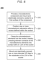
- FIG. 6 illustrates a flow chart 300 showing an example assembly method for the microelectronic system 10, 110, 210a, or 210b.
- a microelectronic component 12 may be provided, and a socket 20 may be mounted and electrically connected to the first surface 16 of the microelectronic component.
- Conductive masses 18 may be used to electrically connect conductive pads 32 exposed at the first surface 34 of the substrate 30 with conductive pads 14 exposed at the first surface 16 of the microelectronic component 12.
- one or more microelectronic elements 40 may be positioned within a recess 22 defined within the socket 20, such that element contacts 42 of the microelectronic elements contact an LGA 60 comprising either conductive pads 58 or top surfaces of a plurality of socket pins 50.
- the microelectronic elements 40 may be clamped into the socket 20, so that the element contacts 42 of the microelectronic elements are pressed into contact with the LGA 60.
- the method may include block 340, in which one or more of discrete IVR dies 270a may be mounted to some of the conductive pads 232 exposed at the first surface 234 of the substrate 230, or one or more discrete IVR dies 270b may be mounted to a portion of the LGA 260, adjacent to the microelectronic elements 240.
- microelectronic systems 10, 110, 210a, and 210b shown in FIGS. 1-5 are just a few examples of the microelectronic system.
- Other microelectronic systems are contemplated, such as systems having different numbers of microelectronic elements, IVR dies, and socket pins.
- the microelectronic systems 10, 110, 210a, and 210b may each include one, two, three, four, six, eight, ten, twelve, sixteen, or thirty-two microelectronic elements, among others.
- the substrates are shown in the figures as being flip-chip mounted to the microelectronic component 12, 112, and 212, in other examples, the microelectronic component may have bond windows extending therethrough, and the substrates may be wire-bonded to the microelectronic component through the bond windows.
- the bond metals used in figures 1-5 are shown as solder bumps, this need not be the case.
- other electrically conductive bond materials may be used (e.g., a conductive matrix material), or rigid conductive pillars may be used to provide an electrical connection between one or more of the elements and the substrate.
- microelectronic systems 10, 110, 210a, 210b disclosed herein may be used in various electronic systems.
- the microelectronic component 12, 112, and 212 may be module cards or module substrates that are configured to be mounted to a motherboard of an electronic device such as a personal computer or a cellular phone, among others.
Landscapes
- Engineering & Computer Science (AREA)
- Microelectronics & Electronic Packaging (AREA)
- Connecting Device With Holders (AREA)
- Physics & Mathematics (AREA)
- Geometry (AREA)
- Manufacturing & Machinery (AREA)
Abstract
Description
- This application claims the benefit of the filing date of
United States Provisional Patent Application No. 63/399,300 filed August 19, 2022 - Semiconductor die and package sizes can vary, and assembly yield loss and long-term reliability issues with conventional BGA (ball grid array) packages could impact the total cost of a computer system. Due to signal and power integrity concerns, BGA packages are generally used to mount next generation ASICs including CPUs and TPUs. However, BGA packages cannot be easily replaced when they fail, due to the use of mounting of the packages directly to circuit panels with conductive masses such as solder.
- LGA (land grid array) socket solutions are more easily replaceable than BGA systems. However, existing LGA socket solutions cannot support high-speed I/O memory and high-power devices. Furthermore, existing LGA/socket systems may have signal integrity issues, such as reflection loss due to impedance discontinuity and/or high crosstalk, due to a difficulty in shielding the signal pins. Existing LGA systems may also have power and power integrity issues, such as power loss due to high pin contact resistance and/or a large signal to noise ratio due to high pin inductance. Also, existing LGA socket solutions cannot support multi-dies or packages, since such solutions have a one-to-one package/socket connection.
- One aspect of the disclosure provides a microelectronic system. According to one aspect, microelectronic system may include a microelectronic component having electrically conductive elements exposed at a first surface thereof, a socket mounted to a first surface of the microelectronic component and including a substrate embedded therein, one or more microelectronic elements each having active semiconductor devices therein and each having element contacts exposed at a front face thereof, and a plurality of socket pins mounted to and extending above the substrate, the socket pins being ground shielded coaxial socket pins. The one or more microelectronic elements may be disposed at least partially within a recess defined within the socket. The socket may have a land grid array comprising top surfaces of the plurality of the socket pins or electrically conductive pads mounted to corresponding ones of the socket pins, and the element contacts of the one or more microelectronic elements may be pressed into contact with the land grid array.
- According to another aspect, the microelectronic system may include a microelectronic component having electrically conductive elements exposed at a first surface thereof, and a socket mounted to a first surface of the microelectronic component, the socket including a substrate embedded therein, the socket defining a recess therein, a first surface of the substrate facing the first surface of the microelectronic component. The microelectronic system may include one or more microelectronic elements each having active semiconductor devices therein and each having element contacts exposed at a front face thereof, the one or more microelectronic elements being disposed at least partially within the recess of the socket.
- The microelectronic system may include a plurality of socket pins mounted to and extending above a second surface of the substrate, the socket pins being ground shielded coaxial socket pins, each socket pin having an inner pin configured to conduct electrical signals between the substrate and one of the microelectronic elements and an outer shield extending around the inner pin and configured to be electrically connected to a ground potential. The socket may have a land grid array comprising top surfaces of the plurality of the socket pins or electrically conductive pads mounted to corresponding ones of the socket pins, and the element contacts of the one or more microelectronic elements may be pressed into contact with the land grid array.
- The socket may be mounted to the microelectronic component via ball-grid array connections that include electrically conductive masses extending between electrically conductive pads exposed at the first surface of the substrate and the electrically conductive elements exposed at the first surface of the microelectronic component. The substrate may have electrically conductive wires therein electrically connected to the plurality of socket pins and configured to provide communication between the one or more microelectronic elements. The one or more microelectronic elements may be four microelectronic elements. The microelectronic system may include one or more capacitors disposed within the socket adjacent to one or more of the microelectronic elements.
- The one or more microelectronic elements may be packaged together in a single wafer-level microelectronic package. The plurality of socket pins may have a minimum pitch between adjacent ones of the socket pins of about 300 microns to 1 mm. The substrate may include one or more redistribution layers to fan out a smaller minimum pitch between adjacent ones of the socket pins to a larger minimum pitch between adjacent ones of electrically conductive pads exposed at the first surface of the substrate. Each socket pin may have an insulator extending between the inner pin and the outer shield thereof, the insulator electrically isolating the inner pin from the outer shield. The insulator may be, for example, air or another material.
- The socket may include one or more of clamps or alignment guides configured to fix the microelectronic elements within the recess. An electrical connection between the land grid array and the element contacts of the one or more microelectronic elements may be devoid of conductive masses. Each of the one or more microelectronic elements may have an integrated voltage regulator therein. The microelectronic system may include one or more discrete voltage regulators each mounted to the land grid array or the substrate.
- Another aspect of the disclosure provides for a method of assembling a microelectronic system. The method may include providing a microelectronic component having electrically conductive elements exposed at a first surface thereof and mounting a socket to the first surface of the microelectronic component, the socket including a substrate embedded therein, the socket defining a recess therein, a first surface of the substrate facing the first surface of the microelectronic component. The method may include positioning one or more microelectronic elements at least partially within the recess of the socket, each of the one or more microelectronic elements having active semiconductor devices therein and each having element contacts exposed at a front face thereof. The method may include clamping the one or more microelectronic elements into the socket, thereby pressing the element contacts of the one or more microelectronic elements into contact with a land grid array of the socket.
- The land grid array of the socket may include top surfaces of a plurality of socket pins or electrically conductive pads mounted to corresponding ones of the socket pins. The plurality of socket pins may be mounted to and may extend above a second surface of the substrate. The socket pins may be ground shielded coaxial socket pins. Each socket pin may have an inner pin configured to conduct electrical signals between the substrate and one of the microelectronic elements and an outer shield extending around the inner pin and configured to be electrically connected to a ground potential.
- The socket may be mounted to the microelectronic component via ball-grid array connections that include electrically conductive masses extending between electrically conductive pads exposed at the first surface of the substrate and the electrically conductive elements exposed at the first surface of the microelectronic component. The clamping may be performed by one or more of clamps or alignment guides that fix the one or more microelectronic elements within the recess. Each socket pin may have an insulator extending between the inner pin and the outer shield thereof. The insulator may electrically isolate the inner pin from the outer shield. Each of the one or more microelectronic elements may have an integrated voltage regulator therein.
-
-
FIG. 1 shows a top plan view of a microelectronic system having a socket thereon, in accordance with aspects of the disclosure. -
FIG. 2 shows a sectional view of the microelectronic system ofFIG. 1 . -
FIG. 3 shows a sectional view of a microelectronic system having a socket thereon, in accordance with aspects of the disclosure. -
FIG. 4 shows a sectional view of a microelectronic system having a socket thereon, in accordance with aspects of the disclosure. -
FIG. 5 shows a sectional view of a microelectronic system having a socket thereon, in accordance with aspects of the disclosure. -
FIG. 6 is a flow chart illustrating an example method in accordance with one aspect of the disclosure. - The systems of the present disclosure implement a land grid array (LGA) with a socket that will enable easy swapping, which can improve long term sustainability of devices that incorporate the system. The new socket concept with improved signal/power integrity and multiple dies or packages may enable an improvement in total cost of ownership compared to conventional systems. The system enables easy swapping of electrically faulty chips (intermittent correctable and permanent uncorrectable errors) for both processors and memory, and/or easy upgrading of dies or packages.
- The system permits a signal integrity improvement over conventional LGA/socket systems due to a coaxial pin design, that improves per-pin crosstalk and impedance discontinuity. The system also may provide a power integrity improvement due to inclusion of a low contact resistance pin, and an integrated voltage regulator (IVR) die to reduce per pin current. The IVR may be a voltage regulator which has higher switching frequency and bandwidth as compared to conventional on-board voltage regulators.
- The systems of the present disclosure include a socket structure for improved signal integrity and multiple die or package (wafer level fan-out chip scale package) configurations. The socket has an embedded substrate or interposer to provide a chip-to-chip communication channel and a BGA connection to another electronic component such as a motherboard. The inclusion of ground shielded coaxial socket pins can solve the signal integrity problems caused by common socket pins, such as impedance discontinuity and crosstalk.
- One example of the present disclosure includes dies with integrated voltage regulators (IVRs) for improved power integrity, which can solve the power or power integrity issue caused by high socket pin inductance and contact resistance. Since an IVR input voltage is high (e.g., 5V), the current requirement per pin is much less. Therefore, the power loss from the socket pins will be dramatically reduced. An IVR system has a much higher loop bandwidth than a conventional system which can eliminate most of the need for capacitors in the system.
- Referring to
FIGS. 1-3 , anexample microelectronic system 10 includes asocket 20 mounted to amicroelectronic component 12, such as a motherboard. Thesocket 20 may be mounted to electricallyconductive pads 14 exposed at afirst surface 16 of themicroelectronic component 12 via ball-grid array (BGA) connections, which may include electricallyconductive masses 18, such as solder balls. Theconductive masses 18 and all other conductive masses described herein may be microbumps having a minimum pitch between adjacent microbumps of about 40-50 microns. In some examples, the minimum pitch between adjacent ones of theconductive masses 18 may be about 1 mm. - The
socket 20 may include asubstrate 30 embedded therein that has electricallyconductive pads 32 exposed at afirst surface 34 thereof. The electricallyconducive pads 32 may be connected to the electricallyconductive masses 18, thereby providing electrical connections between thesocket 20 and themicroelectronic component 12. - The
substrate 30 may be a dielectric element such as an FR-4 (glass-reinforced epoxy resin laminate) circuit panel, for example. Thesubstrate 30 may alternatively be made of or may include another dielectric material such as glass or epoxy, or the substrate may be made of or include a semiconductor material such as silicon, germanium, or gallium arsenide. - The
system 10 may include one or moremicroelectronic elements 40, shown inFIGS. 1 and 2 asmicroelectronic elements microelectronic elements 40 may each include a die or a wafer level chip scale package (WLCSP), or similar packaged part. Themicroelectronic elements 40 may each have active semiconductor devices therein and may each haveelement contacts 42 exposed at afront face 44 thereof. Eachmicroelectronic element 40 may include one or more memory, such as dynamic random access memory (DRAM), or application specific integrated circuits (ASICs) therein. In some examples, themicroelectronic elements 40 may each be processors such as CPUs or GPU machine learning processors, that together are multiple-core processors. In such examples, thesystem 10 may provide a shorter electrical communication path between themicroelectronic elements 40 compared to conventional solutions, thereby providing a performance improvement. Thesubstrate 30 may have electricallyconductive wires 36 therein configured to provide communication between themicroelectronic elements 40. Eachmicroelectronic element 40 may have a semiconductor substrate and dielectric passivation layers overlying top and bottom major planar surfaces thereof, for example. -
FIG. 1 shows fourmicroelectronic elements 40a through 40d, but in other examples thesystem 10 may include other numbers ofmicroelectronic elements 40, such as one, two, three, six, eight, ten, twelve, sixteen, or thirty-two, among others.FIG. 1 shows the fourmicroelectronic elements 40 in a two-by-two square arrangement, but in other examples, that need not be the case. For examples, themicroelectronic elements 40 may be arranged in a single row, four equal rows, eight equal rows, or rows with an unequal number of microelectronic elements, among others. In other examples, the arrangement ofmicroelectronic elements 40 may include one or more capacitors adjacent to one or more of the microelectronic elements. In some examples, thesystem 10 may include some or all of themicroelectronic elements 40a through 40d packaged together in a single wafer-level microelectronic package. - The
system 10 may include a plurality of socket pins 50 mounted to and extending above asecond surface 38 of thesubstrate 30. The socket pins 50 may be electrically connected to theconductive wires 36. The socket pins 50 may have a minimum pitch between adjacent ones of the socket pins of about 300 microns to 1 mm. Thesubstrate 30 may include one or more redistribution layers (RDLs) to fan out a smaller minimum pitch between adjacent ones of the socket pins 50 to a larger minimum pitch between adjacent ones of theconductive masses 18 or between adjacent ones of the electricallyconductive pads 32. - The socket pins 50 may be ground shielded coaxial socket pins. Each socket pin 50 may have an
inner pin 52 configured to conduct electrical signals between thesubstrate 30 and one of themicroelectronic elements 40 and anouter shield 54 extending around the inner pin and configured to be electrically connected to a ground potential. Eachouter shield 54 may be cylindrical in shape. While in some examples theouter shield 54 may be substantially equally spaced apart from a correspondinginner pin 52 disposed therein, in other examples the spacing may vary. The ground shielded coaxial socket pins 50 may solve the signal integrity problems of conventional socket pins, such as impedance discontinuity and crosstalk. Each socket pin 50 may have aninsulator 56 extending between theinner pin 52 and theouter shield 54. Theinsulator 56 may electrically isolate theinner pin 52 from theouter shield 54 and may be air or a dielectric material, among others. - The
system 10 may include a land grid array (LGA) 60 comprising electricallyconductive pads 58. Each electricallyconductive pad 58 may be mounted to a corresponding one of the plurality of socket pins 50. In some examples, the electricallyconductive pads 58 may be omitted, and top surfaces of the socket pins 50 may together comprise theLGA 60. TheLGA 60 may have an arrangement of socket pins 50, such as a first number of pins extending along a first direction and a second number of pins extending along a second direction.. - The
socket 20 may be configured to at least partially receive one or moremicroelectronic elements 40 therein in arecess 22 defined within the socket. The socket may include one or more clamps and/or alignment guides to fix themicroelectronic elements 40 within therecess 22, with theelement contacts 42 of the microelectronic elements being pressed into contact with the LGA 60 (the electricallyconductive pads 58 or the top surfaces of the socket pins 50). The LGA electrical connection between themicroelectronic elements 40 and the socket pins 50 can be done with or without the use of a conductive mass, such as solder. - Now referring to
FIG. 3 , anexample microelectronic system 110 is shown that is a variation of thesystem 10. Thesystem 110 is the same as themicroelectronic system 10, except that each of themicroelectronic elements 140 has an integrated voltage regulator (IVR) 170 therein. Having themicroelectronic elements 140 with integrated voltage regulators (IVRs) may provide improved power integrity. Since an IVR input voltage is high (e.g., 5V), the current requirement per pin is much less. Therefore, the power loss from the socket pins 150 may be dramatically reduced. - Each
microelectronic element 140 may have anIVR 170 integrated together in a single die or package, or each microelectronic element may be stacked with and electrically connected with an IVR adjacent thereto. The interface between eachmicroelectronic element 140 andadjacent IVR 170 may use conductive masses such as solder balls, or the interface may have direct copper-to-copper bonding between confronting contact elements of the microelectronic element and IVR. - Now referring to
FIGS. 4 and 5 , examplemicroelectronic systems system 110. Thesystems microelectronic system 110, except that they include discrete IVR dies 270a and 270b instead of integrated IVR functionality. Thesystem 210a ofFIG. 4 has a discrete IVR die 270a that is mounted to some of theconductive pads 232 exposed at thefirst surface 234 of thesubstrate 230. Thesystem 210b ofFIG. 5 has a discrete IVR die 270b that is mounted to a portion of theLGA 260, adjacent to themicroelectronic elements 240. - Now referring to
FIG. 6 , a method of assembling a microelectronic system will be described. The following operations do not have to be performed in the precise order described below. Rather, various operations can be handled in a different order or simultaneously, and operations may also be added or omitted.FIG. 6 illustrates aflow chart 300 showing an example assembly method for themicroelectronic system - In
block 310, amicroelectronic component 12 may be provided, and asocket 20 may be mounted and electrically connected to thefirst surface 16 of the microelectronic component.Conductive masses 18 may be used to electrically connectconductive pads 32 exposed at thefirst surface 34 of thesubstrate 30 withconductive pads 14 exposed at thefirst surface 16 of themicroelectronic component 12. - In
block 320, one or moremicroelectronic elements 40 may be positioned within arecess 22 defined within thesocket 20, such thatelement contacts 42 of the microelectronic elements contact anLGA 60 comprising eitherconductive pads 58 or top surfaces of a plurality of socket pins 50. Inblock 330, themicroelectronic elements 40 may be clamped into thesocket 20, so that theelement contacts 42 of the microelectronic elements are pressed into contact with theLGA 60. - In some examples, (e.g.,
FIGS. 4 and 5 ) the method may include block 340, in which one or more of discrete IVR dies 270a may be mounted to some of theconductive pads 232 exposed at thefirst surface 234 of thesubstrate 230, or one or more discrete IVR dies 270b may be mounted to a portion of theLGA 260, adjacent to themicroelectronic elements 240. - The design of the
microelectronic systems FIGS. 1-5 are just a few examples of the microelectronic system. Other microelectronic systems are contemplated, such as systems having different numbers of microelectronic elements, IVR dies, and socket pins. For example, themicroelectronic systems - Although the substrates are shown in the figures as being flip-chip mounted to the
microelectronic component figures 1-5 are shown as solder bumps, this need not be the case. In other examples, other electrically conductive bond materials may be used (e.g., a conductive matrix material), or rigid conductive pillars may be used to provide an electrical connection between one or more of the elements and the substrate. - The
microelectronic systems microelectronic component - Unless otherwise stated, the foregoing alternative examples are not mutually exclusive, but may be implemented in various combinations to achieve unique advantages. As these and other variations and combinations of the features discussed above can be utilized without departing from the subject matter defined by the claims, the foregoing description of the example implementations should be taken by way of illustration rather than by way of limitation of the subject matter defined by the claims. In addition, the provision of the examples described herein, as well as clauses phrased as "such as," "including" and the like, should not be interpreted as limiting the subject matter of the claims to the specific examples; rather, the examples are intended to illustrate only one of many possible implementations. Further, the same reference numbers in different drawings can identify the same or similar elements.
Claims (15)
- A microelectronic system, comprising:a microelectronic component having electrically conductive elements exposed at a first surface thereof;a socket mounted to a first surface of the microelectronic component, the socket including a substrate embedded therein, the socket defining a recess therein, a first surface of the substrate facing the first surface of the microelectronic component;one or more microelectronic elements each having active semiconductor devices therein and each having element contacts exposed at a front face thereof, the one or more microelectronic elements being disposed at least partially within the recess of the socket;a plurality of socket pins mounted to and extending above a second surface of the substrate, the socket pins being ground shielded coaxial socket pins, each socket pin having an inner pin configured to conduct electrical signals between the substrate and one of the microelectronic elements and an outer shield extending around the inner pin and configured to be electrically connected to a ground potential,wherein the socket has a land grid array comprising top surfaces of the plurality of the socket pins or electrically conductive pads mounted to corresponding ones of the socket pins, and the element contacts of the one or more microelectronic elements are pressed into contact with the land grid array.
- The microelectronic system of claim 1, wherein the socket is mounted to the microelectronic component via ball-grid array connections that include electrically conductive masses extending between electrically conductive pads exposed at the first surface of the substrate and the electrically conductive elements exposed at the first surface of the microelectronic component.
- The microelectronic system of any one of claims 1 or 2, wherein the substrate has electrically conductive wires therein electrically connected to the plurality of socket pins and configured to provide communication between the one or more microelectronic elements.
- The microelectronic system of any one of the preceding claims, wherein the one or more microelectronic elements comprises four or more microelectronic elements.
- The microelectronic system of any one of the preceding claims, further comprising one or more capacitors disposed within the socket adjacent to one or more of the microelectronic elements.
- The microelectronic system of any one of the preceding claims, wherein the one or more microelectronic elements are packaged together in a single wafer-level microelectronic package.
- The microelectronic system of any one of the preceding claims, wherein the plurality of socket pins has a minimum pitch between adjacent ones of the socket pins of about 300 microns to 1 mm.
- The microelectronic system of any one of the preceding claims, wherein the substrate includes one or more redistribution layers to fan out a smaller minimum pitch between adjacent ones of the socket pins to a larger minimum pitch between adjacent ones of electrically conductive pads exposed at the first surface of the substrate.
- The microelectronic system of any one of the preceding claims, wherein each socket pin has an insulator extending between the inner pin and the outer shield thereof, the insulator electrically isolating the inner pin from the outer shield, and
wherein the insulator is optionally air. - The microelectronic system of any one of the preceding claims, wherein the socket includes one or more of clamps or alignment guides configured to fix the microelectronic elements within the recess.
- The microelectronic system of any one of the preceding claims, wherein an electrical connection between the land grid array and the element contacts of the one or more microelectronic elements is devoid of conductive masses.
- The microelectronic system of any one of the preceding claims, wherein each of the one or more microelectronic elements has an integrated voltage regulator therein, and/or
further comprising one or more discrete voltage regulators each mounted to the land grid array or the substrate. - A method of assembling a microelectronic system, the method comprising:providing a microelectronic component having electrically conductive elements exposed at a first surface thereof;mounting a socket to the first surface of the microelectronic component, the socket including a substrate embedded therein, the socket defining a recess therein, a first surface of the substrate facing the first surface of the microelectronic component;positioning one or more microelectronic elements at least partially within the recess of the socket, each of the one or more microelectronic elements having active semiconductor devices therein and each having element contacts exposed at a front face thereof;clamping the one or more microelectronic elements into the socket, thereby pressing the element contacts of the one or more microelectronic elements into contact with a land grid array of the socket,wherein the land grid array of the socket comprises top surfaces of a plurality of socket pins or electrically conductive pads mounted to corresponding ones of the socket pins, the plurality of socket pins mounted to and extending above a second surface of the substrate, the socket pins being ground shielded coaxial socket pins, each socket pin having an inner pin configured to conduct electrical signals between the substrate and one of the microelectronic elements and an outer shield extending around the inner pin and configured to be electrically connected to a ground potential.
- The method of claim 13, wherein the socket is mounted to the microelectronic component via ball-grid array connections that include electrically conductive masses extending between electrically conductive pads exposed at the first surface of the substrate and the electrically conductive elements exposed at the first surface of the microelectronic component.
- The method of any one of claims 13 or 14, wherein the clamping is performed by one or more of clamps or alignment guides that fix the one or more microelectronic elements within the recess, and/orwherein each socket pin has an insulator extending between the inner pin and the outer shield thereof, the insulator electrically isolating the inner pin from the outer shield, and/orwherein an electrical connection between the land grid array and the element contacts of the one or more microelectronic elements is devoid of conductive masses, and/orwherein each of the one or more microelectronic elements has an integrated voltage regulator therein.
Applications Claiming Priority (2)
| Application Number | Priority Date | Filing Date | Title |
|---|---|---|---|
| US202263399300P | 2022-08-19 | 2022-08-19 | |
| US17/993,240 US12476227B2 (en) | 2022-08-19 | 2022-11-23 | Socket to support high performance multi-die ASICs |
Publications (2)
| Publication Number | Publication Date |
|---|---|
| EP4326018A1 true EP4326018A1 (en) | 2024-02-21 |
| EP4326018B1 EP4326018B1 (en) | 2026-04-15 |
Family
ID=85278214
Family Applications (1)
| Application Number | Title | Priority Date | Filing Date |
|---|---|---|---|
| EP23156832.0A Active EP4326018B1 (en) | 2022-08-19 | 2023-02-15 | Socket to support high performance multi-die asics |
Country Status (2)
| Country | Link |
|---|---|
| US (2) | US12476227B2 (en) |
| EP (1) | EP4326018B1 (en) |
Citations (3)
| Publication number | Priority date | Publication date | Assignee | Title |
|---|---|---|---|---|
| US5702256A (en) * | 1995-12-28 | 1997-12-30 | Intel Corporation | Land grid array socket for use with integrated circuit modules of different sizes including modules which are larger than the socket |
| US20190385979A1 (en) * | 2018-06-14 | 2019-12-19 | Intel Corporation | Multi-packaging for single-socketing |
| EP3971960A1 (en) * | 2020-09-18 | 2022-03-23 | INTEL Corporation | Microelectronic assemblies with inductors in direct bonding regions |
Family Cites Families (25)
| Publication number | Priority date | Publication date | Assignee | Title |
|---|---|---|---|---|
| US7149095B2 (en) * | 1996-12-13 | 2006-12-12 | Tessera, Inc. | Stacked microelectronic assemblies |
| US6812718B1 (en) | 1999-05-27 | 2004-11-02 | Nanonexus, Inc. | Massively parallel interface for electronic circuits |
| US6780057B2 (en) | 2001-12-21 | 2004-08-24 | Intel Corporation | Coaxial dual pin sockets for high speed I/O applications |
| US6937045B2 (en) | 2002-07-18 | 2005-08-30 | Aries Electronics, Inc. | Shielded integrated circuit probe |
| JP3950795B2 (en) | 2002-10-31 | 2007-08-01 | タイコエレクトロニクスアンプ株式会社 | Socket for LGA package |
| US6916195B2 (en) | 2003-03-26 | 2005-07-12 | Intel Corporation | Land grid array socket loading device |
| US7628617B2 (en) | 2003-06-11 | 2009-12-08 | Neoconix, Inc. | Structure and process for a contact grid array formed in a circuitized substrate |
| US7113408B2 (en) | 2003-06-11 | 2006-09-26 | Neoconix, Inc. | Contact grid array formed on a printed circuit board |
| US20050120553A1 (en) | 2003-12-08 | 2005-06-09 | Brown Dirk D. | Method for forming MEMS grid array connector |
| US6916181B2 (en) | 2003-06-11 | 2005-07-12 | Neoconix, Inc. | Remountable connector for land grid array packages |
| US6932618B1 (en) | 2003-05-14 | 2005-08-23 | Xilinx, Inc. | Mezzanine integrated circuit interconnect |
| US7070419B2 (en) | 2003-06-11 | 2006-07-04 | Neoconix Inc. | Land grid array connector including heterogeneous contact elements |
| US8026611B2 (en) * | 2005-12-01 | 2011-09-27 | Tessera, Inc. | Stacked microelectronic packages having at least two stacked microelectronic elements adjacent one another |
| US8212580B2 (en) | 2007-04-02 | 2012-07-03 | Google Inc. | Scalable wideband probes, fixtures, and sockets for high speed IC testing and interconnects |
| US8116097B2 (en) | 2007-11-02 | 2012-02-14 | Oracle America, Inc. | Apparatus for electrically coupling a semiconductor package to a printed circuit board |
| US9613841B2 (en) | 2009-06-02 | 2017-04-04 | Hsio Technologies, Llc | Area array semiconductor device package interconnect structure with optional package-to-package or flexible circuit to package connection |
| US9276339B2 (en) | 2009-06-02 | 2016-03-01 | Hsio Technologies, Llc | Electrical interconnect IC device socket |
| US8952516B2 (en) * | 2011-04-21 | 2015-02-10 | Tessera, Inc. | Multiple die stacking for two or more die |
| JP2014146504A (en) | 2013-01-29 | 2014-08-14 | Wells Cti Kk | Coaxial pin and socket using the same |
| US8786069B1 (en) * | 2013-03-15 | 2014-07-22 | Invensas Corporation | Reconfigurable pop |
| US9178328B2 (en) * | 2013-06-28 | 2015-11-03 | Intel Corporation | Shielded sockets for microprocessors and fabrication thereof by overmolding and plating |
| US9490560B2 (en) | 2014-12-19 | 2016-11-08 | Intel Corporation | Multi-array bottom-side connector using spring bias |
| US9490195B1 (en) * | 2015-07-17 | 2016-11-08 | Invensas Corporation | Wafer-level flipped die stacks with leadframes or metal foil interconnects |
| US10910748B2 (en) * | 2017-11-13 | 2021-02-02 | Te Connectivity Corporation | Cable socket connector assembly for an electronic |
| US11291133B2 (en) | 2018-03-28 | 2022-03-29 | Intel Corporation | Selective ground flood around reduced land pad on package base layer to enable high speed land grid array (LGA) socket |
-
2022
- 2022-11-23 US US17/993,240 patent/US12476227B2/en active Active
-
2023
- 2023-02-15 EP EP23156832.0A patent/EP4326018B1/en active Active
-
2025
- 2025-09-16 US US19/330,447 patent/US20260018571A1/en active Pending
Patent Citations (3)
| Publication number | Priority date | Publication date | Assignee | Title |
|---|---|---|---|---|
| US5702256A (en) * | 1995-12-28 | 1997-12-30 | Intel Corporation | Land grid array socket for use with integrated circuit modules of different sizes including modules which are larger than the socket |
| US20190385979A1 (en) * | 2018-06-14 | 2019-12-19 | Intel Corporation | Multi-packaging for single-socketing |
| EP3971960A1 (en) * | 2020-09-18 | 2022-03-23 | INTEL Corporation | Microelectronic assemblies with inductors in direct bonding regions |
Also Published As
| Publication number | Publication date |
|---|---|
| US12476227B2 (en) | 2025-11-18 |
| EP4326018B1 (en) | 2026-04-15 |
| US20260018571A1 (en) | 2026-01-15 |
| US20240096859A1 (en) | 2024-03-21 |
Similar Documents
| Publication | Publication Date | Title |
|---|---|---|
| US10861824B2 (en) | Microelectronic device packages, stacked microelectronic device packages, and methods for manufacturing microelectronic devices | |
| US7375419B2 (en) | Stacked mass storage flash memory package | |
| US6927484B2 (en) | Stack arrangement of a memory module | |
| US9030021B2 (en) | Printed circuit board having hexagonally aligned bump pads for substrate of semiconductor package, and semiconductor package including the same | |
| US20060087013A1 (en) | Stacked multiple integrated circuit die package assembly | |
| US20050090050A1 (en) | Stacked semiconductor packages | |
| JP2009506553A (en) | Microelectronic device package, stacked microelectronic device package, and method of manufacturing microelectronic device | |
| US9917073B2 (en) | Reconstituted wafer-level package dram with conductive interconnects formed in encapsulant at periphery of the package | |
| KR20110053233A (en) | Package with Power and Ground Through Vias | |
| EP4326018A1 (en) | Socket to support high performance multi-die asics | |
| CN117594579A (en) | Sockets supporting high-performance multi-die ASICs | |
| CN117276266A (en) | A stacked package | |
| HK40109064A (en) | Socket to support high performance multi-die asics | |
| US20240014140A1 (en) | Fan-out Wafer Level Package having Small Interposers | |
| EP4621846A1 (en) | Systems, methods, and devices for semiconductor packaging with wafer on wafer operations | |
| TW202401693A (en) | A package-on-package | |
| CN120379275A (en) | Chip packaging structure and electronic devices |
Legal Events
| Date | Code | Title | Description |
|---|---|---|---|
| PUAI | Public reference made under article 153(3) epc to a published international application that has entered the european phase |
Free format text: ORIGINAL CODE: 0009012 |
|
| STAA | Information on the status of an ep patent application or granted ep patent |
Free format text: STATUS: THE APPLICATION HAS BEEN PUBLISHED |
|
| AK | Designated contracting states |
Kind code of ref document: A1 Designated state(s): AL AT BE BG CH CY CZ DE DK EE ES FI FR GB GR HR HU IE IS IT LI LT LU LV MC ME MK MT NL NO PL PT RO RS SE SI SK SM TR |
|
| STAA | Information on the status of an ep patent application or granted ep patent |
Free format text: STATUS: REQUEST FOR EXAMINATION WAS MADE |
|
| 17P | Request for examination filed |
Effective date: 20240821 |
|
| RBV | Designated contracting states (corrected) |
Designated state(s): AL AT BE BG CH CY CZ DE DK EE ES FI FR GB GR HR HU IE IS IT LI LT LU LV MC ME MK MT NL NO PL PT RO RS SE SI SK SM TR |
|
| GRAP | Despatch of communication of intention to grant a patent |
Free format text: ORIGINAL CODE: EPIDOSNIGR1 |
|
| STAA | Information on the status of an ep patent application or granted ep patent |
Free format text: STATUS: GRANT OF PATENT IS INTENDED |
|
| RIC1 | Information provided on ipc code assigned before grant |
Ipc: H05K 7/10 20060101AFI20251014BHEP |
|
| INTG | Intention to grant announced |
Effective date: 20251106 |
|
| GRAS | Grant fee paid |
Free format text: ORIGINAL CODE: EPIDOSNIGR3 |
|
| GRAA | (expected) grant |
Free format text: ORIGINAL CODE: 0009210 |
|
| STAA | Information on the status of an ep patent application or granted ep patent |
Free format text: STATUS: THE PATENT HAS BEEN GRANTED |
|
| AK | Designated contracting states |
Kind code of ref document: B1 Designated state(s): AL AT BE BG CH CY CZ DE DK EE ES FI FR GB GR HR HU IE IS IT LI LT LU LV MC ME MK MT NL NO PL PT RO RS SE SI SK SM TR |
|
| REG | Reference to a national code |
Ref country code: CH Ref legal event code: F10 Free format text: ST27 STATUS EVENT CODE: U-0-0-F10-F00 (AS PROVIDED BY THE NATIONAL OFFICE) Effective date: 20260415 |
|
| REG | Reference to a national code |
Ref country code: CH Ref legal event code: R17 Free format text: ST27 STATUS EVENT CODE: U-0-0-R10-R17 (AS PROVIDED BY THE NATIONAL OFFICE) Effective date: 20260416 |
|
| REG | Reference to a national code |
Ref country code: DE Ref legal event code: R096 Ref document number: 602023015138 Country of ref document: DE |