EP4325746A1 - Coherent receiver with polarization diversity clock detection - Google Patents

Coherent receiver with polarization diversity clock detection Download PDF

Info

Publication number
EP4325746A1
EP4325746A1 EP23191074.6A EP23191074A EP4325746A1 EP 4325746 A1 EP4325746 A1 EP 4325746A1 EP 23191074 A EP23191074 A EP 23191074A EP 4325746 A1 EP4325746 A1 EP 4325746A1
Authority
EP
European Patent Office
Prior art keywords
clock
squares
sum
polarization
signal
Prior art date
Legal status (The legal status is an assumption and is not a legal conclusion. Google has not performed a legal analysis and makes no representation as to the accuracy of the status listed.)
Pending
Application number
EP23191074.6A
Other languages
German (de)
French (fr)
Inventor
Chen Chen
Current Assignee (The listed assignees may be inaccurate. Google has not performed a legal analysis and makes no representation or warranty as to the accuracy of the list.)
Marvell Asia Pte Ltd
Original Assignee
Marvell Asia Pte Ltd
Priority date (The priority date is an assumption and is not a legal conclusion. Google has not performed a legal analysis and makes no representation as to the accuracy of the date listed.)
Filing date
Publication date
Application filed by Marvell Asia Pte Ltd filed Critical Marvell Asia Pte Ltd
Publication of EP4325746A1 publication Critical patent/EP4325746A1/en
Pending legal-status Critical Current

Links

Images

Classifications

    • HELECTRICITY
    • H04ELECTRIC COMMUNICATION TECHNIQUE
    • H04BTRANSMISSION
    • H04B10/00Transmission systems employing electromagnetic waves other than radio-waves, e.g. infrared, visible or ultraviolet light, or employing corpuscular radiation, e.g. quantum communication
    • H04B10/60Receivers
    • H04B10/61Coherent receivers
    • H04B10/612Coherent receivers for optical signals modulated with a format different from binary or higher-order PSK [X-PSK], e.g. QAM, DPSK, FSK, MSK, ASK
    • HELECTRICITY
    • H04ELECTRIC COMMUNICATION TECHNIQUE
    • H04BTRANSMISSION
    • H04B10/00Transmission systems employing electromagnetic waves other than radio-waves, e.g. infrared, visible or ultraviolet light, or employing corpuscular radiation, e.g. quantum communication
    • H04B10/60Receivers
    • H04B10/61Coherent receivers
    • H04B10/616Details of the electronic signal processing in coherent optical receivers
    • H04B10/6162Compensation of polarization related effects, e.g., PMD, PDL
    • HELECTRICITY
    • H04ELECTRIC COMMUNICATION TECHNIQUE
    • H04BTRANSMISSION
    • H04B10/00Transmission systems employing electromagnetic waves other than radio-waves, e.g. infrared, visible or ultraviolet light, or employing corpuscular radiation, e.g. quantum communication
    • H04B10/60Receivers
    • H04B10/61Coherent receivers
    • H04B10/616Details of the electronic signal processing in coherent optical receivers
    • H04B10/6165Estimation of the phase of the received optical signal, phase error estimation or phase error correction
    • HELECTRICITY
    • H04ELECTRIC COMMUNICATION TECHNIQUE
    • H04BTRANSMISSION
    • H04B10/00Transmission systems employing electromagnetic waves other than radio-waves, e.g. infrared, visible or ultraviolet light, or employing corpuscular radiation, e.g. quantum communication
    • H04B10/60Receivers
    • H04B10/61Coherent receivers
    • H04B10/614Coherent receivers comprising one or more polarization beam splitters, e.g. polarization multiplexed [PolMux] X-PSK coherent receivers, polarization diversity heterodyne coherent receivers
    • HELECTRICITY
    • H04ELECTRIC COMMUNICATION TECHNIQUE
    • H04BTRANSMISSION
    • H04B10/00Transmission systems employing electromagnetic waves other than radio-waves, e.g. infrared, visible or ultraviolet light, or employing corpuscular radiation, e.g. quantum communication
    • H04B10/60Receivers
    • H04B10/61Coherent receivers
    • H04B10/616Details of the electronic signal processing in coherent optical receivers
    • H04B10/6161Compensation of chromatic dispersion
    • HELECTRICITY
    • H04ELECTRIC COMMUNICATION TECHNIQUE
    • H04BTRANSMISSION
    • H04B10/00Transmission systems employing electromagnetic waves other than radio-waves, e.g. infrared, visible or ultraviolet light, or employing corpuscular radiation, e.g. quantum communication
    • H04B10/60Receivers
    • H04B10/61Coherent receivers
    • H04B10/616Details of the electronic signal processing in coherent optical receivers
    • H04B10/6164Estimation or correction of the frequency offset between the received optical signal and the optical local oscillator
    • HELECTRICITY
    • H04ELECTRIC COMMUNICATION TECHNIQUE
    • H04LTRANSMISSION OF DIGITAL INFORMATION, e.g. TELEGRAPHIC COMMUNICATION
    • H04L7/00Arrangements for synchronising receiver with transmitter
    • H04L7/0075Arrangements for synchronising receiver with transmitter with photonic or optical means

Definitions

  • the present disclosure relates generally to optical communication, and particularly to methods and systems for clock detection in electro-optical receivers.
  • An electro-optical receiver typically receives and demodulates an optical signal comprising a sequence of modulated symbols.
  • a coherent receiver which demodulates the phase, or both the amplitude and the phase, of the received signal, a fundamental requirement is to reconstruct a clock signal that defines the timing of the symbol sequence. This task is referred to herein as "clock tone detection” or “clock recovery.”
  • Clock tone detection is important, for example, for synchronizing with the transmitter in order to demodulate the received signal correctly, and for estimating Chromatic Dispersion (CD).
  • An embodiment that is described herein provides a receiver including an optical front-end and digital circuitry.
  • the optical front-end is configured to receive an optical signal including a first optical signal component having a first polarization and a second optical signal component having a second polarization, different from the first polarization, the first optical signal component and the second optical signal component being modulated with symbols at a symbol rate.
  • the digital circuitry is configured to derive a first digital signal representing the first optical signal component having the first polarization, and to derive a second digital signal representing the second optical signal component having the second polarization.
  • the digital circuitry includes a clock detector configured to calculate correlation terms comprising (i) a first autocorrelation of the first digital signal, (ii) a second autocorrelation of the second digital signal, (iii) a first cross-correlation between the first digital signal and the second digital signal, and (iv) a second cross-correlation between the second digital signal and the first digital signal, the correlation terms being calculated in a frequency-domain with a frequency offset commensurate with the symbol rate.
  • the clock detector is configured to recover a clock signal of the symbols by (i) summing selected pairs of the correlation terms, and (ii) calculating or estimating a sum-of-squares of the summed pairs.
  • the clock detector is configured to prevent the recovered clock signal from diminishing to zero for any combination of Polarization Mode Dispersion (PMD), polarization rotation and Differential Group Delay (DGD) affecting the optical signal.
  • PMD Polarization Mode Dispersion
  • DDD Differential Group Delay
  • the clock detector is configured to recover the clock signal by averaging the sum-of-squares over a plurality of frequencies. In an embodiment, the clock detector is configured to approximate squares of the summed pairs by calculating absolute-values of the summed pairs. In another embodiment, the clock detector is configured to approximate the sum-of-squares by (i) calculating respective absolute-values of the summed pairs of the correlation terms, and (ii) taking a maximum of the absolute-values.
  • the clock detector in recovering the clock signal, is configured to recover an amplitude of the clock signal by summing the sum-of-squares over a plurality of frequencies.
  • the clock detector is configured to average each of the correlation terms over time, per frequency among the plurality of frequencies, then calculate the sum-of-squares per frequency based on the averaged correlation terms, and then calculate the amplitude of the clock signal based on the sum-of-squares calculated per frequency.
  • the clock detector is configured to sum each of the correlation terms over the plurality of frequencies, then calculate the sum-of-squares based on the correlation terms summed over the frequencies, and then average multiple sums-of-squares to produce the amplitude of the clock signal.
  • the clock detector is further configured to recover a phase of the clock signal by taking an imaginary part of the calculated or estimated sum-of-squares.
  • a method for clock recovery includes receiving an optical signal including a first optical signal component having a first polarization and a second optical signal component having a second polarization, different from the first polarization, the first optical signal component and the second optical signal component being modulated with symbols at a symbol rate.
  • a first digital signal is derived, representing the first optical signal component having the first polarization
  • a second digital signal is derived, representing the second optical signal component having the second polarization.
  • Correlation terms are calculated, including (i) a first autocorrelation of the first digital signal, (ii) a second autocorrelation of the second digital signal, (iii) a first cross-correlation between the first digital signal and the second digital signal, and (iv) a second cross-correlation between the second digital signal and the first digital signal, the correlation terms being calculated in a frequency-domain with a frequency offset commensurate with the symbol rate.
  • a clock signal of the symbols is recovered by (i) summing selected pairs of the correlation terms, and (ii) calculating or estimating a sum-of-squares of the summed pairs.
  • Embodiments that are described herein provide electro-optical receivers having improved clock tone detection, and associated methods.
  • the disclosed techniques apply polarization diversity to detect the clock tone with high resilience against impairments that affect the received optical signal, such as Polarization Mode Diversity (PMD) and Differential Group Delay (DGD).
  • PMD Polarization Mode Diversity
  • DDD Differential Group Delay
  • Example applications can be used in any suitable system or environment involving reception of optical signals.
  • Example applications include receivers of long-haul optical links, optical interconnects in data centers, and many others.
  • Fig. 1 is a block diagram that schematically illustrates a coherent electro-optical receiver 20, in accordance with an embodiment that is described herein.
  • Receiver 20 receives an optical signal from a transmitter, e.g., over an optical fiber.
  • the optical signal is a dual-polarization signal, having two polarizations denoted x and y .
  • the optical signal is modulated with data using a suitable modulation scheme that utilizes both polarizations, e.g., Quadrature Amplitude Modulation (QAM).
  • QAM Quadrature Amplitude Modulation
  • the optical signal is coherent, in the sense that at least some of the information conveyed by the signal is embedded in the signal phase.
  • receiver 20 comprises an optical front end 24 and digital circuitry 28.
  • optical front end 24 performs optical and analog functions of the receiver
  • digital circuitry 28 performs mixed-signal and digital functions of the receiver.
  • any other suitable task partitioning can be used.
  • Optical front end 24 of receiver 20 receives the optical signal from the optical fiber, down-converts the signal to baseband, splits the baseband signal into the individual polarizations, and then performs complex (In-phase/Quadrature - I/Q) signal detection on each polarization.
  • optical front end 24 outputs four analog baseband electrical signals denoted S xi ( t ), S xq ( t ) , S yi ( t ) and S yq ( t ).
  • Signals S xi ( t ) and S xq ( t ) are the In-phase (I) and Quadrature (Q) components of the x polarization, respectively.
  • Signals S yi ( t ) and S yq ( t ) are the I and Q components of the y polarization, respectively.
  • optical front end 24 comprises a Local Oscillator (LO) laser, a polarization beam splitter, an optical hybrid, photodiodes and Trans-Impedance Amplifiers (TIAs).
  • LO Local Oscillator
  • polarization beam splitter a polarization beam splitter
  • optical hybrid a polarization beam splitter
  • photodiodes a polarization beam splitter
  • TIAs Trans-Impedance Amplifiers
  • Digital circuitry 28 in the embodiment of Fig. 1 comprises four Analog-to-Digital Converters (ADCs) 32, a digital front end 36, a Fast Fourier Transform (FFT) circuit 40, a Chromatic Dispersion (CD) compensation circuit 44, a Digital Signal Processor (DSP) 48, a clock detector 52 and a feedback control circuit 56.
  • ADCs Analog-to-Digital Converters
  • FFT Fast Fourier Transform
  • CD Chromatic Dispersion
  • DSP Digital Signal Processor
  • ADCs 32 digitize (sample) the four signals S xi ( t ), S xq ( t ) , S yi ( t ) and S yq (t ) to produce four corresponding digital baseband signals.
  • Digital front end 36 removes timing skews among the four digital signals, equalizes the amplitudes of the four digital signals, and/or performs any other suitable digital preprocessing.
  • digital front end 36 outputs two signals denoted S x ( t ) and S y ( t ), which are respective digital time-domain representations of the x and y polarizations of the received optical signal.
  • FFT circuit 40 transforms signals S x ( t ) and S y ( t ) from the time domain into the frequency domain, producing two digital frequency-domain signals denoted S x ( ⁇ ) and S y ( ⁇ ) .
  • CD compensation circuit 44 compensates for at least some of the chromatic dispersion in S x ( ⁇ ) and S y ( ⁇ ), originating from the received optical signal.
  • DSP 48 demodulates signals S x ( ⁇ ) and S y ( ⁇ ) and outputs the demodulated data.
  • clock detector 52 is configured to reconstruct a clock tone from signals S x ( ⁇ ) and S y ( ⁇ ). As will be explained and demonstrated below, clock detector 52 uses polarization diversity techniques for detecting the clock tone reliably irrespective of any combination of Polarization Mode Dispersion (PMD), polarization rotation and/or Differential Group Delay (DGD) affecting the received optical signal.
  • PMD Polarization Mode Dispersion
  • DDD Differential Group Delay
  • the detected clock tone can be used by receiver 20 in various ways and for various purposes.
  • digital circuitry 56 further comprises a feedback control circuit 56, which adjusts the sampling phases of ADCs 32 based on the detected clock tone.
  • feedback control circuit comprises a loop filter (e.g., a Proportional Integral Derivative - PID) that filters the detected clock tone.
  • the output of the loop filter controls a Voltage Controlled Oscillator (VCO), which in turn controls the sampling phases of ADCs 32.
  • VCO Voltage Controlled Oscillator
  • feedback control circuit 56 can be implemented in any other suitable manner.
  • the detected clock tone can be used for any other suitable purpose, e.g., to aid in estimating the Chromatic Distortion (CD) as an input to CD compensation circuit 44.
  • CD Chromatic Distortion
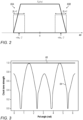
  • Fig. 2 is a diagram that schematically illustrates a frequency-domain representation (spectrum) of a signal received by receiver 20 of Fig. 1 , in accordance with an embodiment that is described herein. Without loss of generality the figure illustrates the spectrum of signal S x ( ⁇ ). The spectrum of S y ( ⁇ ) is similar.
  • the clock tone of such a signal can be estimated in the frequency domain by correlating pairs of frequency-domain samples of the signal, wherein the samples in each pair are separated from one another by a frequency offset equal to the symbol rate ⁇ b .
  • the samples of each pair (one sample from set 60A and a corresponding sample from set 60B) are separated by ⁇ b .
  • a sum of correlations between pairs of frequency-domain samples having this spacing can be used as an estimate of the clock tone.
  • such an estimate is sensitive to signal impairments such as PMD, polarization rotation and DGD.
  • S x 0 ( ⁇ ) and S y 0 ( ⁇ ) denote the two polarizations of the optical signal transmitted by the transmitter, i.e., before any PMD, polarization rotation and DGD occur.
  • ⁇ , ⁇ and ⁇ denote the polarization rotation angle, polarization phase and DGD between the two polarizations at receiver 20, respectively.
  • ⁇ , ⁇ and ⁇ are constant over frequency.
  • ⁇ , ⁇ and ⁇ may depend on frequency ⁇ within the signal bandwidth.
  • the frequency-domain representation used herein enables accounting for any PMD order.
  • the clock tone can be estimated from the x polarization component of the signal by calculating the following sum of correlations:
  • the clock tone can be estimated from the y polarization component of the signal by calculating:
  • Equation 1 and Equation 2 do not include the effects of distortion mechanisms such as polarization rotation, PMD and DGD.
  • PMD and DGD the clock tone estimated from the X polarization is given by:
  • ⁇ ... ⁇ brackets denote statistical expectation, or a time average.
  • Equation 4 also assumes that S x and S y are statistically mutually independent, so that the cross-correlation between them is zero.
  • Analyzing the clock tone estimator of Equation 5 reveals that the amplitude of the estimated clock tone would diminish to zero when the DGD approaches half the symbol rate (i.e., when ⁇ approaches 1/(2 f b ) ) and the polarization rotation angle ⁇ approaches an odd integer multiple of 45 degrees.
  • the clock tone may also diminish under additional combinations of DGD and PMD, e.g., because Equation 5 assumed only first-order PMD.
  • a clock tone that diminishes to zero can have catastrophic effects on the receiver performance, e.g., deviation from the optimal signal sampling points or even complete loss of synchronization with the transmitter.
  • a diminishing clock tone may cause large estimation errors, possibly leading to failure in acquiring the signal.
  • clock detector 52 uses a new, novel estimator for the clock tone, an estimator that does not diminish to zero under any combination of PMD and/or DGD.
  • the estimator of Equation 8 uses autocorrelation (also referred to as intra-polarization correlation) of the x polarization signal;
  • the estimator of Equation 8 uses autocorrelation of the y polarization signal;
  • the estimator of Equation 10 uses cross-correlation (also referred to as inter-polarization correlation) between the x polarization signal and the y polarization signal;
  • the estimator of Equation 11 uses cross-correlation between the y polarization signal and the x polarization signal.
  • the frequency offset is ⁇ b .
  • C yy ⁇ cos ⁇ ⁇ ⁇ ′ cos ⁇ b ⁇ 2 ⁇ ⁇ ⁇ 2 ⁇ ⁇ ⁇ ⁇ ′ 2 + j cos ⁇ + ⁇ ′
  • clock detector 52 estimates the clock tone by diversity-combining the four correlation terms of Equations 12-15 ( C xx ( ⁇ ), C yy ( ⁇ ), C xy ( ⁇ ) and C yx ( ⁇ ) ) in a way that renders the combination insensitive to PMD (of any order) and DGD. In some embodiments, clock detector 52 (i) sums selected pairs of the correlation terms, and (ii) calculates or estimating a sum-of-squares of the summed pairs.
  • C total ( ⁇ ) the sum-of-squares of the summed pairs is denoted C total ( ⁇ ) and is given by:
  • Equation 16 Since C total ( ⁇ ) of Equation 16 has no dependence on PMD of any order and no dependence on polarization rotation, the estimated clock tone C sum of Equation 17, has no dependence on these impairments, as well.
  • Fig. 3 is a graph illustrating the dependence of clock tone strength on polarization angle, in accordance with an embodiment that is described herein.
  • the optical signal used in the present example was a dual-polarization signal having a symbol rate of 64.6GHz. Each of the two polarizations was modulated using 16-QAM modulation. A DGD equal to half the symbol rate (7.7psec) was introduced at the transmitter. A burst of 61440 samples of the dual-polarization signal was captured by the receiver ADC. To generate the graph, various polarization angles ⁇ were applied numerically to the captured signal using a 2-by-2 Jones matrix (as in Equation 1).
  • a plot 64 shows the strength of the detected clock tone as a function of polarization angle, without the disclosed technique (e.g., using Equation 12 or Equation 13). As seen, the clock tone strength is far from being constant, and diminishes to zero at various polarization angles.
  • a plot 68 shows the strength of the detected clock tone as a function of polarization angle when using the disclosed polarization diversity technique (e.g., using Equation 16). As seen, the clock strength is entirely independent of polarization angle and does not diminish to zero.
  • clock detector 52 evaluates another approximation of Equation 16 that replaces the summing operation with a maximum (maximum over the absolute-values of the summed pairs of correlation terms) :
  • C total ⁇ max C xx ⁇ + C yy ⁇ C xx ⁇ ⁇ C yy ⁇ C xy ⁇ + C yx ⁇ C xy ⁇ ⁇ C yx ⁇
  • Equations 18 and 19 require considerably less computational power than the exact calculation of Equation 16.
  • Fig. 4 is a graph illustrating a dependence of clock tone strength on polarization angle for various calculations or approximations of Equation 16, in accordance with an embodiment that is described herein.
  • the signal properties in the present example are the same as in the example of Fig. 3 above.
  • Fig. 5 is a flow chart that schematically illustrates a method for clock tone detection, in accordance with an embodiment that is described herein.
  • the method begins with optical front end 24 of receiver 20 receiving a dual-polarization optical signal, at a reception operation 80.
  • digitization and transforming operation 84 the following operations are performed:
  • clock detector 52 calculates the frequency-domain autocorrelation terms C xx ( ⁇ ) and C yy ( ⁇ ) (also referred to as intra-polarization correlation terms) and the frequency-domain cross-correlation terms C xy ( ⁇ ) and C yx ( ⁇ ) (also referred to as inter-polarization correlation terms.
  • clock detector 52 calculates or approximates C total ( ⁇ ), e.g., using an exact calculation in accordance with Equation 16 or using an approximation in accordance with Equation 18 or 19.
  • clock detector 52 sums C total ( ⁇ ) over multiple frequencies and takes the absolute value of the sum (e.g., in accordance with Equation 17), to obtain the estimated amplitude C sum of the clock tone.
  • Fig. 6 is a block diagram that schematically illustrates a clock detector 100, in accordance with an embodiment that is described herein.
  • the configuration of Fig. 6 can be used to implement clock detector 52 in receiver 20 ( Fig. 1 ).
  • Clock detector 100 comprises four correlators 104, four respective averaging blocks 108, a diversity combiner 112 and a summing block 116.
  • each correlator 104 is provided to a respective averaging block 108.
  • Each averaging block 108 averages the respective correlation term over N clock cycles, to produce an estimate of the long-time average (and thus of the expectancy) of the correlation term.
  • Diversity combiner 112 calculates (or approximates) C total ( ⁇ ) for each frequency ⁇ . Any of Equations 16, 18 and 19 can be used for this purpose. Summing block 116 then calculates C sum based on the C total ( ⁇ ) values according to Equation 17.
  • Fig. 7 is a block diagram that schematically illustrates a clock detector 120, in accordance with another embodiment that is described herein. This configuration, too, can be used to implement clock detector 52 of receiver 20.
  • Clock detector 120 comprises four correlators 104, four corresponding summing blocks 128, a diversity combiner 132 and an averaging block 136.
  • Correlators 104 receive signals S x ( ⁇ ) and S y ( ⁇ ) from FFT circuit 40. For each frequency ⁇ in the range of 2 L + 1 frequencies ( Fig. 2 ), correlators 104 calculate four respective correlation terms according to Equations 20-23.
  • Equations 28-30 are similar to Equations 16, 18 and 19 above, respectively, except that the former use time-averaged correlation terms instead of raw correlation terms. Note that in the embodiment of Fig. 7 , C total is not a function of frequency.
  • averaging block 136 averages multiple values of C total to improve estimation accuracy in the presence of noise.
  • the resulting average is an estimate of the clock tone amplitude.
  • the description up to this point referred mainly to obtaining the amplitude of the clock tone from the received signal.
  • the clock tone detector may use various techniques for estimating the phase of the clock tone.
  • C total ⁇ Im C xx ⁇ + C yy ⁇ 2 + C xx ⁇ ⁇ C yy ⁇ 2 C xy ⁇ + C yx ⁇ 2 + C xy ⁇ ⁇ C yx ⁇ 2
  • the Im operator denotes the imaginary part of a complex value.
  • Equations 31 and 32 are modified versions of Equations 16 and 28, respectively.
  • receiver 20 and its various components are example configurations that are depicted solely for the sake of clarity. In alternative embodiments, any other suitable configurations can be used.
  • the different elements of receiver 20 and its various components, such as clock detectors 52, 100 and 120 may be implemented using dedicated hardware or firmware, such as using hard-wired or programmable logic, e.g., in an Application-Specific Integrated Circuit (ASIC) or Field-Programmable Gate Array (FPGA). Additionally, or alternatively, some functions of receiver 20, such as clock detector 52, 100 or 120, may be implemented in software and/or using a combination of hardware and software elements. Elements that are not mandatory for understanding of the disclosed techniques have been omitted from the figure for the sake of clarity.
  • some functions of the disclosed receivers may be implemented in one or more programmable processors, e.g., one or more Central Processing Units (CPUs), microcontrollers and/or Digital Signal Processors (DSPs), which are programmed in software to carry out the functions described herein.
  • the software may be downloaded to any of the processors in electronic form, over a network, for example, or it may, alternatively or additionally, be provided and/or stored on non-transitory tangible media, such as magnetic, optical, or electronic memory.
  • the embodiments described herein mainly address clock tone detection in coherent optical receivers
  • the methods and systems described herein can also be used in other applications, such as in any other system or application that involves a polarization-multiplexed signal, such as in various Radio-Frequency (RF) and optical communication systems.
  • RF Radio-Frequency

Landscapes

  • Physics & Mathematics (AREA)
  • Engineering & Computer Science (AREA)
  • Computer Networks & Wireless Communication (AREA)
  • Signal Processing (AREA)
  • Electromagnetism (AREA)
  • Optics & Photonics (AREA)
  • Optical Communication System (AREA)

Abstract

A receiver includes an optical front-end and digital circuitry. The optical front-end is configured to receive an optical signal including first and second optical signal components having first and second polarizations and modulated with symbols at a symbol rate. The digital circuitry is configured to derive first and second digital signals representing the first and second optical signal components having the first and second polarizations. The digital circuitry includes a clock detector configured to calculate correlation terms, the correlation terms being calculated in a frequency-domain with a frequency offset commensurate with the symbol rate. The clock detector is configured to recover a clock signal of the symbols by (i) summing selected pairs of the correlation terms, and (ii) calculating or estimating a sum-of-squares of the summed pairs.

Description

    CROSS-REFERENCE TO RELATED APPLICATIONS
  • This application claims the benefit of U.S. Provisional Patent Application 63/398,893, filed August 18, 2022 , whose disclosure is incorporated herein by reference.
  • FIELD OF THE DISCLOSURE
  • The present disclosure relates generally to optical communication, and particularly to methods and systems for clock detection in electro-optical receivers.
  • BACKGROUND
  • An electro-optical receiver typically receives and demodulates an optical signal comprising a sequence of modulated symbols. In a coherent receiver, which demodulates the phase, or both the amplitude and the phase, of the received signal, a fundamental requirement is to reconstruct a clock signal that defines the timing of the symbol sequence. This task is referred to herein as "clock tone detection" or "clock recovery." Clock tone detection is important, for example, for synchronizing with the transmitter in order to demodulate the received signal correctly, and for estimating Chromatic Dispersion (CD).
  • The description above is presented as a general overview of related art in this field and should not be construed as an admission that any of the information it contains constitutes prior art against the present patent application.
  • SUMMARY
  • An embodiment that is described herein provides a receiver including an optical front-end and digital circuitry. The optical front-end is configured to receive an optical signal including a first optical signal component having a first polarization and a second optical signal component having a second polarization, different from the first polarization, the first optical signal component and the second optical signal component being modulated with symbols at a symbol rate. The digital circuitry is configured to derive a first digital signal representing the first optical signal component having the first polarization, and to derive a second digital signal representing the second optical signal component having the second polarization. The digital circuitry includes a clock detector configured to calculate correlation terms comprising (i) a first autocorrelation of the first digital signal, (ii) a second autocorrelation of the second digital signal, (iii) a first cross-correlation between the first digital signal and the second digital signal, and (iv) a second cross-correlation between the second digital signal and the first digital signal, the correlation terms being calculated in a frequency-domain with a frequency offset commensurate with the symbol rate. The clock detector is configured to recover a clock signal of the symbols by (i) summing selected pairs of the correlation terms, and (ii) calculating or estimating a sum-of-squares of the summed pairs.
  • In some embodiments, by estimating the sum of squares, the clock detector is configured to prevent the recovered clock signal from diminishing to zero for any combination of Polarization Mode Dispersion (PMD), polarization rotation and Differential Group Delay (DGD) affecting the optical signal.
  • In some embodiments, the clock detector is configured to recover the clock signal by averaging the sum-of-squares over a plurality of frequencies. In an embodiment, the clock detector is configured to approximate squares of the summed pairs by calculating absolute-values of the summed pairs. In another embodiment, the clock detector is configured to approximate the sum-of-squares by (i) calculating respective absolute-values of the summed pairs of the correlation terms, and (ii) taking a maximum of the absolute-values.
  • In some embodiments, in recovering the clock signal, the clock detector is configured to recover an amplitude of the clock signal by summing the sum-of-squares over a plurality of frequencies. In an example embodiment, the clock detector is configured to average each of the correlation terms over time, per frequency among the plurality of frequencies, then calculate the sum-of-squares per frequency based on the averaged correlation terms, and then calculate the amplitude of the clock signal based on the sum-of-squares calculated per frequency. In an alternative embodiment, the clock detector is configured to sum each of the correlation terms over the plurality of frequencies, then calculate the sum-of-squares based on the correlation terms summed over the frequencies, and then average multiple sums-of-squares to produce the amplitude of the clock signal.
  • In a disclosed embodiment, the clock detector is further configured to recover a phase of the clock signal by taking an imaginary part of the calculated or estimated sum-of-squares.
  • There is additionally provided, in accordance with an embodiment that is described herein, a method for clock recovery. The method includes receiving an optical signal including a first optical signal component having a first polarization and a second optical signal component having a second polarization, different from the first polarization, the first optical signal component and the second optical signal component being modulated with symbols at a symbol rate. A first digital signal is derived, representing the first optical signal component having the first polarization, and a second digital signal is derived, representing the second optical signal component having the second polarization. Correlation terms are calculated, including (i) a first autocorrelation of the first digital signal, (ii) a second autocorrelation of the second digital signal, (iii) a first cross-correlation between the first digital signal and the second digital signal, and (iv) a second cross-correlation between the second digital signal and the first digital signal, the correlation terms being calculated in a frequency-domain with a frequency offset commensurate with the symbol rate. A clock signal of the symbols is recovered by (i) summing selected pairs of the correlation terms, and (ii) calculating or estimating a sum-of-squares of the summed pairs.
  • The present disclosure will be more fully understood from the following detailed description of the embodiments thereof, taken together with the drawings in which:
  • BRIEF DESCRIPTION OF THE DRAWINGS
    • Fig. 1 is a block diagram that schematically illustrates a coherent electro-optical receiver, in accordance with an embodiment that is described herein;
    • Fig. 2 is a diagram that schematically illustrates a frequency-domain representation of a signal received by the receiver of Fig. 1, in accordance with an embodiment that is described herein;
    • Figs. 3 and 4 are graphs illustrating the dependence of clock tone strength on polarization angle for various clock tone estimation schemes, in accordance with embodiments that are described herein;
    • Fig. 5 is a flow chart that schematically illustrates a method for clock tone detection, in accordance with an embodiment that is described herein; and
    • Figs. 6 and 7 are block diagrams that schematically illustrate example implementations of a clock detector, in accordance with embodiments that are described herein.
    DETAILED DESCRIPTION OF EMBODIMENTS
  • Embodiments that are described herein provide electro-optical receivers having improved clock tone detection, and associated methods. As will be explained herein, the disclosed techniques apply polarization diversity to detect the clock tone with high resilience against impairments that affect the received optical signal, such as Polarization Mode Diversity (PMD) and Differential Group Delay (DGD).
  • The disclosed techniques can be used in any suitable system or environment involving reception of optical signals. Example applications include receivers of long-haul optical links, optical interconnects in data centers, and many others.
  • Fig. 1 is a block diagram that schematically illustrates a coherent electro-optical receiver 20, in accordance with an embodiment that is described herein. Receiver 20 receives an optical signal from a transmitter, e.g., over an optical fiber. The optical signal is a dual-polarization signal, having two polarizations denoted x and y . The optical signal is modulated with data using a suitable modulation scheme that utilizes both polarizations, e.g., Quadrature Amplitude Modulation (QAM). The optical signal is coherent, in the sense that at least some of the information conveyed by the signal is embedded in the signal phase. In the present example, receiver 20 comprises an optical front end 24 and digital circuitry 28. Typically, optical front end 24 performs optical and analog functions of the receiver, whereas digital circuitry 28 performs mixed-signal and digital functions of the receiver. Alternatively, however, any other suitable task partitioning can be used.
  • Optical front end 24 of receiver 20 receives the optical signal from the optical fiber, down-converts the signal to baseband, splits the baseband signal into the individual polarizations, and then performs complex (In-phase/Quadrature - I/Q) signal detection on each polarization. In the present example, optical front end 24 outputs four analog baseband electrical signals denoted Sxi (t), Sxq (t), Syi (t) and Syq (t). Signals Sxi (t) and Sxq (t) are the In-phase (I) and Quadrature (Q) components of the x polarization, respectively. Signals Syi (t) and Syq (t) are the I and Q components of the y polarization, respectively.
  • In a typical implementation, optical front end 24 comprises a Local Oscillator (LO) laser, a polarization beam splitter, an optical hybrid, photodiodes and Trans-Impedance Amplifiers (TIAs). The internal structure of optical front end 24 is not detailed in the figure, for the sake of clarity. In alternative embodiments, any other suitable configuration can be used.
  • Digital circuitry 28 in the embodiment of Fig. 1 comprises four Analog-to-Digital Converters (ADCs) 32, a digital front end 36, a Fast Fourier Transform (FFT) circuit 40, a Chromatic Dispersion (CD) compensation circuit 44, a Digital Signal Processor (DSP) 48, a clock detector 52 and a feedback control circuit 56.
  • In an embodiment, ADCs 32 digitize (sample) the four signals Sxi (t), Sxq (t), Syi (t) and Syq(t) to produce four corresponding digital baseband signals. Digital front end 36 removes timing skews among the four digital signals, equalizes the amplitudes of the four digital signals, and/or performs any other suitable digital preprocessing. In the present example digital front end 36 outputs two signals denoted Sx (t) and Sy (t), which are respective digital time-domain representations of the x and y polarizations of the received optical signal.
  • In an embodiment, FFT circuit 40 transforms signals Sx (t) and Sy (t) from the time domain into the frequency domain, producing two digital frequency-domain signals denoted Sx (ω) and Sy (ω). CD compensation circuit 44 compensates for at least some of the chromatic dispersion in Sx (ω) and Sy (ω), originating from the received optical signal. DSP 48 demodulates signals Sx (ω) and Sy (ω) and outputs the demodulated data.
  • In disclosed embodiments, clock detector 52 is configured to reconstruct a clock tone from signals Sx (ω) and Sy (ω). As will be explained and demonstrated below, clock detector 52 uses polarization diversity techniques for detecting the clock tone reliably irrespective of any combination of Polarization Mode Dispersion (PMD), polarization rotation and/or Differential Group Delay (DGD) affecting the received optical signal. Example clock detector implementations are described further below with reference to Figs. 6 and 7.
  • In various embodiments, the detected clock tone can be used by receiver 20 in various ways and for various purposes. In the example embodiment of Fig. 1, digital circuitry 56 further comprises a feedback control circuit 56, which adjusts the sampling phases of ADCs 32 based on the detected clock tone. In an example embodiment, feedback control circuit comprises a loop filter (e.g., a Proportional Integral Derivative - PID) that filters the detected clock tone. The output of the loop filter controls a Voltage Controlled Oscillator (VCO), which in turn controls the sampling phases of ADCs 32. In alternative embodiments, feedback control circuit 56 can be implemented in any other suitable manner. Additionally, or alternatively, the detected clock tone can be used for any other suitable purpose, e.g., to aid in estimating the Chromatic Distortion (CD) as an input to CD compensation circuit 44.
  • Fig. 2 is a diagram that schematically illustrates a frequency-domain representation (spectrum) of a signal received by receiver 20 of Fig. 1, in accordance with an embodiment that is described herein. Without loss of generality the figure illustrates the spectrum of signal Sx (ω). The spectrum of Sy (ω) is similar.
  • It can be shown that the clock tone of such a signal can be estimated in the frequency domain by correlating pairs of frequency-domain samples of the signal, wherein the samples in each pair are separated from one another by a frequency offset equal to the symbol rate ωb . The example of Fig. 2 shows a first set 60A of 2L+1 samples centered about ω = - ωb /2, and a second set 60B of 2L+1 samples centered about ω = ωb /2. The samples of each pair (one sample from set 60A and a corresponding sample from set 60B) are separated by ωb . A sum of correlations between pairs of frequency-domain samples having this spacing can be used as an estimate of the clock tone. As will be shown below, however, such an estimate is sensitive to signal impairments such as PMD, polarization rotation and DGD.
  • Let S x0(ω) and S y0(ω) denote the two polarizations of the optical signal transmitted by the transmitter, i.e., before any PMD, polarization rotation and DGD occur. Let θ, ϕ and τ denote the polarization rotation angle, polarization phase and DGD between the two polarizations at receiver 20, respectively. With this notation, the signals Sx (ω) and Sy (ω) at the input of clock detector 52 are given by: S x ω S y ω = cosθe sinθ sinθ cosθe e τ 2 0 0 e τ 2 S x 0 ω S y 0 ω = cosθe e τ 2 S x 0 ω + sinθe τ 2 S y 0 ω sinθe τ 2 S x 0 ω + cosθe τ 2 S y 0 ω
    Figure imgb0001
  • For first-order PMD, θ , ϕ and τ are constant over frequency. When considering higher-order PMD, θ, ϕ and τ may depend on frequency ω within the signal bandwidth. The frequency-domain representation used herein enables accounting for any PMD order.
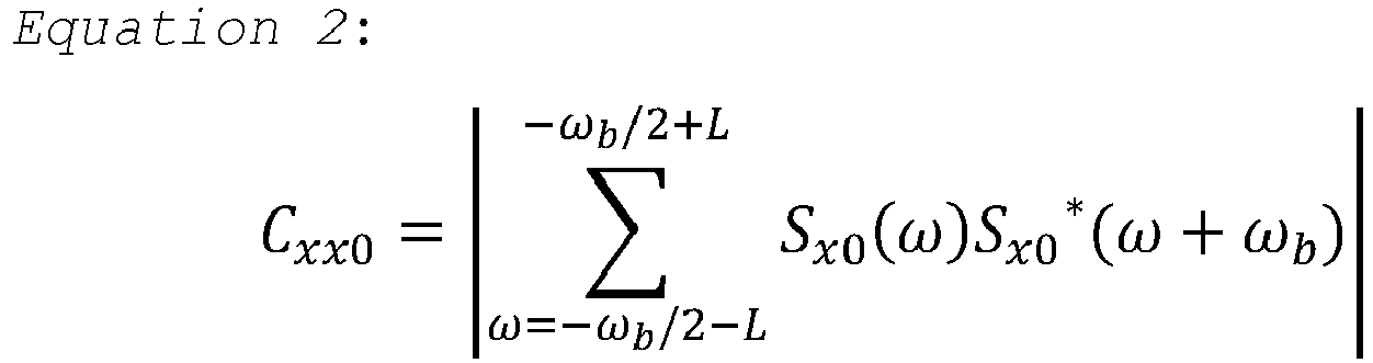
  • As noted above, the clock tone can be estimated from the x polarization component of the signal by calculating the following sum of correlations: C xx 0 = ω = ω b / 2 L ω b / 2 + L S x 0 ω S x 0 * ω + ω b
    Figure imgb0002
  • Similarly, the clock tone can be estimated from the y polarization component of the signal by calculating: C yy 0 = ω = ω b / 2 L ω b / 2 + L S y 0 ω S y 0 * ω + ω b
    Figure imgb0003
  • Both Equation 1 and Equation 2 do not include the effects of distortion mechanisms such as polarization rotation, PMD and DGD. After introducing polarization rotation, PMD and DGD according to Equation 1, the clock tone estimated from the X polarization is given by: C xx ω = S x ω S x * ω + ω b = cos 2 θe b τ 2 C xx 0 ω + sin 2 θe b τ 2 C yy 0 ω
    Figure imgb0004
    wherein the 〈...〉 brackets denote statistical expectation, or a time average. With sufficient averaging over time, the terms S x 0 ω S x 0 ω + ω b
    Figure imgb0005
    and S y 0 ω S y 0 ω + ω b
    Figure imgb0006
    converge to constant values represented by C xx0(ω) and C yy0(ω), respectively. Equation 4 also assumes that Sx and Sy are statistically mutually independent, so that the cross-correlation between them is zero.
  • In practice, the signals in the x and y polarizations have the same energy, and therefore C xx0(ω) = C yy0(ω). Under this condition Equation 4 becomes: C xx ω = cos πf b τ jcos 2 θ sin πf b τ C xx 0 ω
    Figure imgb0007
    wherein fb = ω/2π.
  • Analyzing the clock tone estimator of Equation 5 reveals that the amplitude of the estimated clock tone would diminish to zero when the DGD approaches half the symbol rate (i.e., when τ approaches 1/(2fb )) and the polarization rotation angle θ approaches an odd integer multiple of 45 degrees. In practice, the clock tone may also diminish under additional combinations of DGD and PMD, e.g., because Equation 5 assumed only first-order PMD.
  • A clock tone that diminishes to zero can have catastrophic effects on the receiver performance, e.g., deviation from the optimal signal sampling points or even complete loss of synchronization with the transmitter. When the recovered clock tone is used for CD estimation, a diminishing clock tone may cause large estimation errors, possibly leading to failure in acquiring the signal.
  • In view of the foregoing, in some embodiments clock detector 52 uses a new, novel estimator for the clock tone, an estimator that does not diminish to zero under any combination of PMD and/or DGD.
  • Consider a pair of frequencies ω and ω + ωb . Without loss of generality, the two frequencies can be assumed to differ in polarization rotation angle ( θ vs. θ ), polarization phase ( ϕ' vs. ϕ ) and DGD ( τ + Δτ vs. τ ). The frequency-domain samples of the x polarization signal at these two frequencies can thus be written as: S x ω = cosθe e τ + Δ τ 2 S x 0 ω + sinθe τ + Δ τ 2 S y 0 ω
    Figure imgb0008
    S x ω + ω b = cosθ e e j ω + ω b τ 2 S x 0 ω + ω b + sinθ e j ω + ω b τ 2 S y 0 ω + ω b
    Figure imgb0009
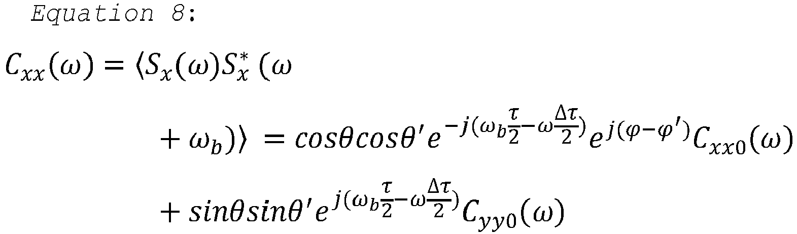
  • The clock tone estimated from this pair of samples is given by the following correlation term: C xx ω = S x ω S x * ω + ω b = cosθcosθ e j ω b τ 2 ω Δ τ 2 e j ϕ ϕ C xx 0 ω + sinθsinθ e j ω b τ 2 ω Δ τ 2 C yy 0 ω
    Figure imgb0010
  • In a similar manner, it is possible to estimate the clock tone using any of the following correlation terms: C yy ω = S y ω S y * ω + ω b
    Figure imgb0011
    C xy ω = S x ω S y * ω + ω b
    Figure imgb0012
    C yx ω = S y ω S x * ω + ω b
    Figure imgb0013
  • The estimator of Equation 8 uses autocorrelation (also referred to as intra-polarization correlation) of the x polarization signal; The estimator of Equation 8 uses autocorrelation of the y polarization signal; The estimator of Equation 10 uses cross-correlation (also referred to as inter-polarization correlation) between the x polarization signal and the y polarization signal; The estimator of Equation 11 uses cross-correlation between the y polarization signal and the x polarization signal. In all these correlation terms the frequency offset is ωb .
  • Assuming the x and y polarization signal have the same energy, we can normalize C xx0(ω) = C yy0(ω) = 1 without loss of generality. The autocorrelation (intra-polarization correlation) terms of Equations 8 and 9 and the cross-correlation (inter-polarization correlation) terms of Equations 10 and 11 can be expressed as: C xx ω = cos θ θ cos ω b τ 2 ω Δ τ 2 ϕ ϕ 2 j cos θ + θ sin ω b τ 2 ω Δ τ 2 ϕ ϕ 2 e j ϕ ϕ 2
    Figure imgb0014
    C yy ω = cos θ θ cos ω b τ 2 ω Δ τ 2 ϕ ϕ 2 + j cos θ + θ sin ω b τ 2 ω Δ τ 2 ϕ ϕ 2 e j ϕ ϕ 2
    Figure imgb0015
    C xy ω = cos θ θ cos ω b τ 2 ω Δ τ 2 ϕ ϕ 2 + j sin θ + θ sin ω b τ 2 ω Δ τ 2 ϕ ϕ 2 e j ϕ ϕ 2
    Figure imgb0016
    C yx ω = sin θ θ cos ω b τ 2 ω Δ τ 2 ϕ ϕ 2 + j sin θ + θ sin ω b τ 2 ω Δ τ 2 ϕ ϕ 2 e j ϕ ϕ 2
    Figure imgb0017
  • Each of the estimators of Equations 12-15, if taken individually, depends on PMD and DGD and will diminish to zero in some combinations of these impairments. In some embodiments, clock detector 52 estimates the clock tone by diversity-combining the four correlation terms of Equations 12-15 ( Cxx (ω), Cyy (ω), Cxy (ω) and Cyx (ω)) in a way that renders the combination insensitive to PMD (of any order) and DGD. In some embodiments, clock detector 52 (i) sums selected pairs of the correlation terms, and (ii) calculates or estimating a sum-of-squares of the summed pairs. In an embodiment, the sum-of-squares of the summed pairs is denoted Ctotal (ω) and is given by: C total ω = C xx ω + C yy ω 2 + C xx ω C yy ω 2 + C xy ω + C yx ω 2 + C xy ω C yx ω 2 = C xx 0 ω
    Figure imgb0018
  • As discussed with regards to Equations 2 and 3 above, the clock tone can be estimated by calculating: C sum = ω = ω b / 2 L ω b / 2 + L C total ω
    Figure imgb0019
  • Since Ctotal (ω) of Equation 16 has no dependence on PMD of any order and no dependence on polarization rotation, the estimated clock tone Csum of Equation 17, has no dependence on these impairments, as well.
  • Fig. 3 is a graph illustrating the dependence of clock tone strength on polarization angle, in accordance with an embodiment that is described herein. The optical signal used in the present example was a dual-polarization signal having a symbol rate of 64.6GHz. Each of the two polarizations was modulated using 16-QAM modulation. A DGD equal to half the symbol rate (7.7psec) was introduced at the transmitter. A burst of 61440 samples of the dual-polarization signal was captured by the receiver ADC. To generate the graph, various polarization angles θ were applied numerically to the captured signal using a 2-by-2 Jones matrix (as in Equation 1).
  • A plot 64 shows the strength of the detected clock tone as a function of polarization angle, without the disclosed technique (e.g., using Equation 12 or Equation 13). As seen, the clock tone strength is far from being constant, and diminishes to zero at various polarization angles. A plot 68 shows the strength of the detected clock tone as a function of polarization angle when using the disclosed polarization diversity technique (e.g., using Equation 16). As seen, the clock strength is entirely independent of polarization angle and does not diminish to zero.
  • In some embodiments (e.g., in the above example of Fig. 3) clock detector 52 estimates the clock tone by evaluating Equation 16 exactly. This exact calculation includes evaluating Equation 16 2L + 1 times. Exact evaluation of Equation 16, however, is computationally expensive, especially since it includes four squaring operations per frequency. In some embodiments, instead of an accurate evaluation, clock detector 52 evaluates an approximation of Equation 16 that replaces the squares (of the summed pairs of correlation terms) with absolute-values: C total ω = C xx ω + C yy ω + C xx ω C yy ω + C xy ω + C yx ω + C xy ω C yx ω
    Figure imgb0020
  • In other embodiments, clock detector 52 evaluates another approximation of Equation 16 that replaces the summing operation with a maximum (maximum over the absolute-values of the summed pairs of correlation terms) : C total ω = max C xx ω + C yy ω C xx ω C yy ω C xy ω + C yx ω C xy ω C yx ω
    Figure imgb0021
  • The approximations in Equations 18 and 19 require considerably less computational power than the exact calculation of Equation 16.
  • Fig. 4 is a graph illustrating a dependence of clock tone strength on polarization angle for various calculations or approximations of Equation 16, in accordance with an embodiment that is described herein. The signal properties in the present example are the same as in the example of Fig. 3 above.
  • Plot 64 (no polarization diversity) and plot 68 (exact calculation of Equation 16) are reproduced in Fig. 4 again as a reference. In addition, a plot 72 shows the clock tone strength when approximated using Equation 18; and a plot 76 shows the clock tone strength when approximated using Equation 19. As seen, the approximations of Equations 18 and 19 do introduce some dependency on polarization rotation angle, but the dependency is sufficiently weak to ensure that the estimated clock tone never diminishes to zero. As such, the approximations of Equations 18 and 19 provide a good trade-off between performance and computational complexity.
  • Fig. 5 is a flow chart that schematically illustrates a method for clock tone detection, in accordance with an embodiment that is described herein. The method begins with optical front end 24 of receiver 20 receiving a dual-polarization optical signal, at a reception operation 80. At a detection, digitization and transforming operation 84, the following operations are performed:
    • ▪ Optical front end 24 converts the optical signal into the analog baseband electrical signals Sxi (t), Sxq (t), Syi (t) and Syq (t).
    • ▪ ADCs 32 digitize the analog baseband electrical signals to produce respective digital baseband electrical signals.
    • ▪ Digital front end 36 pre-processes the digital baseband electrical signals to produce the two complex digital signals Sx (t) and Sy (t).
    • FFT circuit 40 transforms signals Sx (t) and Sy (t) into digital frequency-domain signals Sx (ω) and Sy (ω), respectively.
  • At a correlation calculation operation 88, clock detector 52 calculates the frequency-domain autocorrelation terms Cxx (ω) and Cyy (ω) (also referred to as intra-polarization correlation terms) and the frequency-domain cross-correlation terms Cxy (ω) and Cyx (ω) (also referred to as inter-polarization correlation terms.
  • At a diversity combining operation 92, clock detector 52 calculates or approximates Ctotal (ω), e.g., using an exact calculation in accordance with Equation 16 or using an approximation in accordance with Equation 18 or 19. At a summing operation 96, clock detector 52 sums Ctotal (ω) over multiple frequencies and takes the absolute value of the sum (e.g., in accordance with Equation 17), to obtain the estimated amplitude Csum of the clock tone.
  • Fig. 6 is a block diagram that schematically illustrates a clock detector 100, in accordance with an embodiment that is described herein. The configuration of Fig. 6 can be used to implement clock detector 52 in receiver 20 (Fig. 1). Clock detector 100 comprises four correlators 104, four respective averaging blocks 108, a diversity combiner 112 and a summing block 116.
  • Correlators 104 receive signals Sx (ω) and Sy (ω) from FFT circuit 40. For each frequency ω in the range of 2L + 1 frequencies (Fig. 2), correlators 104 calculate four respective correlation terms: C xx ω = S x ω S x * ω + ω b
    Figure imgb0022
    C yy ω = S y ω S y * ω + ω b
    Figure imgb0023
    C xy ω = S x ω S y * ω + ω b
    Figure imgb0024
    C yx ω = S y ω S y * ω + ω b
    Figure imgb0025
  • The output of each correlator 104 is provided to a respective averaging block 108. Each averaging block 108 averages the respective correlation term over N clock cycles, to produce an estimate of the long-time average (and thus of the expectancy) of the correlation term.
  • Diversity combiner 112 calculates (or approximates) Ctotal (ω) for each frequency ω . Any of Equations 16, 18 and 19 can be used for this purpose. Summing block 116 then calculates Csum based on the Ctotal (ω) values according to Equation 17.
  • Fig. 7 is a block diagram that schematically illustrates a clock detector 120, in accordance with another embodiment that is described herein. This configuration, too, can be used to implement clock detector 52 of receiver 20. Clock detector 120 comprises four correlators 104, four corresponding summing blocks 128, a diversity combiner 132 and an averaging block 136.
  • The initial operations of clock detector 120 are similar to those of clock detector 100 of Fig. 6: Correlators 104 receive signals Sx (ω) and Sy (ω) from FFT circuit 40. For each frequency ω in the range of 2L + 1 frequencies (Fig. 2), correlators 104 calculate four respective correlation terms according to Equations 20-23.
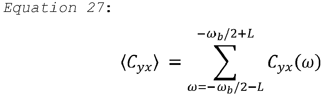
  • In the configuration of Fig. 7, in contrast to Fig. 6, the correlation terms are first summed over frequency, and only then diversity-combined and averaged over time. As seen in the figure, each summing block 128 sums a respective correlation term over the set of frequencies ω in the range of 2L + 1 frequencies, according to Equations 24-27 below: C xx = ω = ω b / 2 L ω b / 2 + L C xx ω
    Figure imgb0026
    C yy = ω = ω b / 2 L ω b / 2 + L C yy ω
    Figure imgb0027
    C xy = ω = ω b / 2 L ω b / 2 + L C xy ω
    Figure imgb0028
    C yx = ω = ω b / 2 L ω b / 2 + L C yx ω
    Figure imgb0029
  • Diversity combiner 132 calculates (or approximates) Ctotal based on the four outputs of summing blocks 128. Any of Equations 28-30 below can be used, Equation 28 being an exact calculation and Equations 29 and 30 being approximations: C total = C xx + C yy 2 + C xx C yy 2 + C xy + C yx 2 + C xy C yx 2
    Figure imgb0030
    C total = C xx + C yy + C xx C yy + C xy + C yx + C xy C yx
    Figure imgb0031
    C total = max C xx + C yy C xx C yy C xy + C yx C xy C xy
    Figure imgb0032
  • Equations 28-30 are similar to Equations 16, 18 and 19 above, respectively, except that the former use time-averaged correlation terms instead of raw correlation terms. Note that in the embodiment of Fig. 7, Ctotal is not a function of frequency.
  • Finally, averaging block 136 averages multiple values of Ctotal to improve estimation accuracy in the presence of noise. The resulting average is an estimate of the clock tone amplitude.
  • The description up to this point referred mainly to obtaining the amplitude of the clock tone from the received signal. In some applications, e.g., for adjusting the sampling phase of ADCs 32 by feedback control circuit 56 (Fig. 1), it is also necessary to estimate the phase of the clock tone. In various embodiments, the clock tone detector may use various techniques for estimating the phase of the clock tone.
  • For example, when using the configuration of Fig. 6, clock tone detector 100 may estimate the phase of the clock tone by calculating: C total ω = Im C xx ω + C yy ω 2 + C xx ω C yy ω 2 C xy ω + C yx ω 2 + C xy ω C yx ω 2
    Figure imgb0033
    wherein the Im operator denotes the imaginary part of a complex value. As another example, when using the configuration of Fig. 7, clock tone detector 120 may estimate the phase of the clock tone by calculating: C total = Im C xx + C yy 2 + C xx C yy 2 + C xy + C yx 2 C xy C yx 2
    Figure imgb0034
  • Equations 31 and 32 are modified versions of Equations 16 and 28, respectively.
  • The configurations of receiver 20 and its various components, such as clock detectors 52, 100 and 120, as shown in Figs. 1, 6 and 7, are example configurations that are depicted solely for the sake of clarity. In alternative embodiments, any other suitable configurations can be used. The different elements of receiver 20 and its various components, such as clock detectors 52, 100 and 120, may be implemented using dedicated hardware or firmware, such as using hard-wired or programmable logic, e.g., in an Application-Specific Integrated Circuit (ASIC) or Field-Programmable Gate Array (FPGA). Additionally, or alternatively, some functions of receiver 20, such as clock detector 52, 100 or 120, may be implemented in software and/or using a combination of hardware and software elements. Elements that are not mandatory for understanding of the disclosed techniques have been omitted from the figure for the sake of clarity.
  • In some embodiments, some functions of the disclosed receivers, e.g., functions of clock detector 52, 100 or 120, may be implemented in one or more programmable processors, e.g., one or more Central Processing Units (CPUs), microcontrollers and/or Digital Signal Processors (DSPs), which are programmed in software to carry out the functions described herein. The software may be downloaded to any of the processors in electronic form, over a network, for example, or it may, alternatively or additionally, be provided and/or stored on non-transitory tangible media, such as magnetic, optical, or electronic memory.
  • Although the embodiments described herein mainly address clock tone detection in coherent optical receivers, the methods and systems described herein can also be used in other applications, such as in any other system or application that involves a polarization-multiplexed signal, such as in various Radio-Frequency (RF) and optical communication systems.
  • It is noted that the embodiments described above are cited by way of example, and that the present invention is not limited to what has been particularly shown and described hereinabove. Rather, the scope of the present invention includes both combinations and sub-combinations of the various features described hereinabove, as well as variations and modifications thereof which would occur to persons skilled in the art upon reading the foregoing description and which are not disclosed in the prior art. Documents incorporated by reference in the present patent application are to be considered an integral part of the application except that to the extent any terms are defined in these incorporated documents in a manner that conflicts with the definitions made explicitly or implicitly in the present specification, only the definitions in the present specification should be considered.
  • The following is a list of further preferred embodiments of the invention:
    • Embodiment 1: A receiver, comprising:
      • an optical front-end, configured to receive an optical signal comprising a first optical signal component having a first polarization and a second optical signal component having a second polarization, different from the first polarization, the first optical signal component and the second optical signal component being modulated with symbols at a symbol rate; and
      • digital circuitry, configured to derive a first digital signal representing the first optical signal component having the first polarization, and derive a second digital signal representing the second optical signal component having the second polarization,
        the digital circuitry comprising a clock detector configured to:
        • calculate correlation terms comprising (i) a first autocorrelation of the first digital signal, (ii) a second autocorrelation of the second digital signal, (iii) a first cross-correlation between the first digital signal and the second digital signal, and (iv) a second cross-correlation between the second digital signal and the first digital signal, the correlation terms being calculated in a frequency-domain with a frequency offset commensurate with the symbol rate; and
        • recover a clock signal of the symbols by (i) summing selected pairs of the correlation terms, and (ii) calculating or estimating a sum-of-squares of the summed pairs.
    • Embodiment 2: The receiver according to embodiment 1, wherein, by estimating the sum of squares, the clock detector is configured to prevent the recovered clock signal from diminishing to zero for any combination of Polarization Mode Dispersion (PMD), polarization rotation and Differential Group Delay (DGD) affecting the optical signal.
    • Embodiment 3: The receiver according to embodiment 1, wherein the clock detector is configured to recover the clock signal by averaging the sum-of-squares over a plurality of frequencies.
    • Embodiment 4: The receiver according to embodiment 1, wherein the clock detector is configured to approximate squares of the summed pairs by calculating absolute-values of the summed pairs.
    • Embodiment 5: The receiver according to embodiment 1, wherein the clock detector is configured to approximate the sum-of-squares by:
      • calculating respective absolute-values of the summed pairs of the correlation terms; and
      • taking a maximum of the absolute-values.
    • Embodiment 6: The receiver according to embodiment 1, wherein, in recovering the clock signal, the clock detector is configured to recover an amplitude of the clock signal by summing the sum-of-squares over a plurality of frequencies.
    • Embodiment 7: The receiver according to embodiment 6, wherein the clock detector is configured to average each of the correlation terms over time, per frequency among the plurality of frequencies, then calculate the sum-of-squares per frequency based on the averaged correlation terms, and then calculate the amplitude of the clock signal based on the sum-of-squares calculated per frequency.
    • Embodiment 8: The receiver according to embodiment 6, wherein the clock detector is configured to sum each of the correlation terms over the plurality of frequencies, then calculate the sum-of-squares based on the correlation terms summed over the frequencies, and then average multiple sums-of-squares to produce the amplitude of the clock signal.
    • Embodiment 9: The receiver according to embodiment 1, wherein the clock detector is further configured to recover a phase of the clock signal by taking an imaginary part of the calculated or estimated sum-of-squares.
    • Embodiment 10: A method for clock recovery, comprising:
      • receiving an optical signal comprising a first optical signal component having a first polarization and a second optical signal component having a second polarization, different from the first polarization, the first optical signal component and the second optical signal component being modulated with symbols at a symbol rate;
      • deriving a first digital signal representing the first optical signal component having the first polarization, and deriving a second digital signal representing the second optical signal component having the second polarization;
      • calculating correlation terms comprising (i) a first autocorrelation of the first digital signal, (ii) a second autocorrelation of the second digital signal, (iii) a first cross-correlation between the first digital signal and the second digital signal, and (iv) a second cross-correlation between the second digital signal and the first digital signal, the correlation terms being calculated in a frequency-domain with a frequency offset commensurate with the symbol rate; and
      • recovering a clock signal of the symbols by (i) summing selected pairs of the correlation terms, and (ii) calculating or estimating a sum-of-squares of the summed pairs.
    • Embodiment 11: The method for clock recovery according to embodiment 10, wherein estimating the sum of squares comprises preventing the recovered clock signal from diminishing to zero for any combination of Polarization Mode Dispersion (PMD), polarization rotation and Differential Group Delay (DGD) affecting the optical signal.
    • Embodiment 12: The method for clock recovery according to embodiment 10, wherein recovering the clock signal comprises averaging the sum-of-squares over a plurality of frequencies.
    • Embodiment 13: The method for clock recovery according to embodiment 10, wherein estimating the sum-of-squares comprises approximating squares of the summed pairs by calculating absolute-values of the summed pairs.
    • Embodiment 14: The method for clock recovery according to embodiment 10, wherein estimating the sum-of-squares comprises:
      • calculating respective absolute-values of the summed pairs of the correlation terms; and
      • taking a maximum of the absolute-values.
    • Embodiment 15: The method for clock recovery according to embodiment 10, wherein recovering the clock signal comprises recovering an amplitude of the clock signal by summing the sum-of-squares over a plurality of frequencies.
    • Embodiment 16: The method for clock recovery according to embodiment 15, wherein recovering the amplitude of the clock signal comprises averaging each of the correlation terms over time, per frequency among the plurality of frequencies, then calculating the sum-of-squares per frequency based on the averaged correlation terms, and then calculating the amplitude of the clock signal based on the sum-of-squares calculated per frequency.
    • Embodiment 17: The method for clock recovery according to embodiment 15, wherein recovering the amplitude of the clock signal comprises summing each of the correlation terms over the plurality of frequencies, then calculating the sum-of-squares based on the correlation terms summed over the frequencies, and then averaging multiple sums-of-squares to produce the amplitude of the clock signal.
    • Embodiment 18: The method for clock recovery according to embodiment 10, wherein recovering the clock signal further comprises recovering a phase of the clock signal by taking an imaginary part of the calculated or estimated sum-of-squares.

Claims (15)

  1. A receiver, comprising:
    an optical front-end, configured to receive an optical signal comprising a first optical signal component having a first polarization and a second optical signal component having a second polarization, different from the first polarization, the first optical signal component and the second optical signal component being modulated with symbols at a symbol rate; and
    digital circuitry, configured to derive a first digital signal representing the first optical signal component having the first polarization, and derive a second digital signal representing the second optical signal component having the second polarization,
    the digital circuitry comprising a clock detector configured to:
    calculate correlation terms comprising (i) a first autocorrelation of the first digital signal, (ii) a second autocorrelation of the second digital signal, (iii) a first cross-correlation between the first digital signal and the second digital signal, and (iv) a second cross-correlation between the second digital signal and the first digital signal, the correlation terms being calculated in a frequency-domain with a frequency offset commensurate with the symbol rate; and
    recover a clock signal of the symbols by (i) summing selected pairs of the correlation terms, and (ii) calculating or estimating a sum-of-squares of the summed pairs.
  2. The receiver according to claim 1, wherein, by estimating the sum of squares, the clock detector is configured to prevent the recovered clock signal from diminishing to zero for any combination of Polarization Mode Dispersion (PMD), polarization rotation and Differential Group Delay (DGD) affecting the optical signal.
  3. The receiver according to claim 1 or 2, wherein the clock detector is configured to:
    recover the clock signal by averaging the sum-of-squares over a plurality of frequencies; and/or
    approximate squares of the summed pairs by calculating absolute-values of the summed pairs.
  4. The receiver according to claim 1 or 2, wherein the clock detector is configured to approximate the sum-of-squares by:
    calculating respective absolute-values of the summed pairs of the correlation terms; and
    taking a maximum of the absolute-values.
  5. The receiver according to any one of claims 1 to 4, wherein, in recovering the clock signal, the clock detector is configured to recover an amplitude of the clock signal by summing the sum-of-squares over a plurality of frequencies.
  6. The receiver according to claim 5, wherein the clock detector is configured to:
    average each of the correlation terms over time, per frequency among the plurality of frequencies, then calculate the sum-of-squares per frequency based on the averaged correlation terms, and then calculate the amplitude of the clock signal based on the sum-of-squares calculated per frequency, and/or
    sum each of the correlation terms over the plurality of frequencies, then calculate the sum-of-squares based on the correlation terms summed over the frequencies, and then average multiple sums-of-squares to produce the amplitude of the clock signal.
  7. The receiver according to any one of claims 1 to 6, wherein the clock detector is further configured to recover a phase of the clock signal by taking an imaginary part of the calculated or estimated sum-of-squares.
  8. A method for clock recovery, comprising:
    receiving an optical signal comprising a first optical signal component having a first polarization and a second optical signal component having a second polarization, different from the first polarization, the first optical signal component and the second optical signal component being modulated with symbols at a symbol rate;
    deriving a first digital signal representing the first optical signal component having the first polarization, and deriving a second digital signal representing the second optical signal component having the second polarization;
    calculating correlation terms comprising (i) a first autocorrelation of the first digital signal, (ii) a second autocorrelation of the second digital signal, (iii) a first cross-correlation between the first digital signal and the second digital signal, and (iv) a second cross-correlation between the second digital signal and the first digital signal, the correlation terms being calculated in a frequency-domain with a frequency offset commensurate with the symbol rate; and
    recovering a clock signal of the symbols by (i) summing selected pairs of the correlation terms, and (ii) calculating or estimating a sum-of-squares of the summed pairs.
  9. The method for clock recovery according to claim 8, wherein estimating the sum of squares comprises preventing the recovered clock signal from diminishing to zero for any combination of Polarization Mode Dispersion (PMD), polarization rotation and Differential Group Delay (DGD) affecting the optical signal.
  10. The method for clock recovery according to claim 8 or 9, wherein recovering the clock signal comprises averaging the sum-of-squares over a plurality of frequencies.
  11. The method for clock recovery according to claim 8, wherein estimating the sum-of-squares comprises approximating squares of the summed pairs by calculating absolute-values of the summed pairs.
  12. The method for clock recovery according to claim 8, wherein estimating the sum-of-squares comprises:
    calculating respective absolute-values of the summed pairs of the correlation terms; and
    taking a maximum of the absolute-values.
  13. The method for clock recovery according to any one of claims 8 to 12, wherein recovering the clock signal comprises recovering an amplitude of the clock signal by summing the sum-of-squares over a plurality of frequencies.
  14. The method for clock recovery according to claim 13, wherein recovering the amplitude of the clock signal comprises:
    averaging each of the correlation terms over time, per frequency among the plurality of frequencies, then calculating the sum-of-squares per frequency based on the averaged correlation terms, and then calculating the amplitude of the clock signal based on the sum-of-squares calculated per frequency; or
    summing each of the correlation terms over the plurality of frequencies, then calculating the sum-of-squares based on the correlation terms summed over the frequencies, and then averaging multiple sums-of-squares to produce the amplitude of the clock signal.
  15. The method for clock recovery according to any one of claims 8 to 14, wherein recovering the clock signal further comprises recovering a phase of the clock signal by taking an imaginary part of the calculated or estimated sum-of-squares.
EP23191074.6A 2022-08-18 2023-08-11 Coherent receiver with polarization diversity clock detection Pending EP4325746A1 (en)

Applications Claiming Priority (1)

Application Number Priority Date Filing Date Title
US202263398893P 2022-08-18 2022-08-18

Publications (1)

Publication Number Publication Date
EP4325746A1 true EP4325746A1 (en) 2024-02-21

Family

ID=87571150

Family Applications (1)

Application Number Title Priority Date Filing Date
EP23191074.6A Pending EP4325746A1 (en) 2022-08-18 2023-08-11 Coherent receiver with polarization diversity clock detection

Country Status (3)

Country Link
US (1) US12381631B2 (en)
EP (1) EP4325746A1 (en)
CN (1) CN117595937A (en)

Citations (2)

* Cited by examiner, † Cited by third party
Publication number Priority date Publication date Assignee Title
US20120219302A1 (en) * 2011-02-28 2012-08-30 Han Henry Sun Pmd and chromatic dispersion tolerant clock recovery
US20170302385A1 (en) * 2012-12-03 2017-10-19 Inphi Corporation Timing recovery for optical coherent receivers in the presence of polarization mode dispersion

Family Cites Families (4)

* Cited by examiner, † Cited by third party
Publication number Priority date Publication date Assignee Title
US7532822B2 (en) * 2005-02-28 2009-05-12 Nortel Networks Limited Clock recovery from an optical signal with polarization impairments
US7522841B2 (en) * 2005-10-21 2009-04-21 Nortel Networks Limited Efficient data transmission and training of data processing functions
CN102612811B (en) 2010-02-20 2016-03-30 华为技术有限公司 Clock phase recovery device
US9225433B1 (en) 2011-08-24 2015-12-29 Clariphy Communications, Inc. Timing recovery for optical coherent receivers in the presence of polarization mode dispersion

Patent Citations (2)

* Cited by examiner, † Cited by third party
Publication number Priority date Publication date Assignee Title
US20120219302A1 (en) * 2011-02-28 2012-08-30 Han Henry Sun Pmd and chromatic dispersion tolerant clock recovery
US20170302385A1 (en) * 2012-12-03 2017-10-19 Inphi Corporation Timing recovery for optical coherent receivers in the presence of polarization mode dispersion

Also Published As

Publication number Publication date
US20240063917A1 (en) 2024-02-22
US12381631B2 (en) 2025-08-05
CN117595937A (en) 2024-02-23

Similar Documents

Publication Publication Date Title
US8774644B2 (en) PMD and chromatic dispersion tolerant clock recovery
EP2584720B1 (en) Frequency offset estimation apparatus, receiver apparatus, frequency offset estimation method, and reception method
US10778496B2 (en) OFDM system synchronization tracking method and apparatus
US8073345B2 (en) Frequency estimation in an intradyne optical receiver
EP3432488B1 (en) Transmission characteristic compensation device, transmission characteristic compensation method, and communication device
EP2942917B1 (en) Optical transmission system, phase compensation method, and optical reception device
EP2436128B1 (en) Clock phase recovery apparatus
EP2930867B1 (en) Light-receiving device and phase cycle slip reduction method
US8401403B2 (en) Timing recovery in presence of optical impairments and optimization of equalization based on timing recovery moment strengths
EP2256960B1 (en) Digital coherent optical receiver
JP6295585B2 (en) Optical communication receiver and frequency offset compensation method
CN102725960B (en) Method for phase and oscillator frequency estimation
US8705986B2 (en) PMD-insensitive method of chromatic dispersion estimation for a coherent receiver
US20100329677A1 (en) Symbol Timing Recovery in Polarization Division Multiplexed Coherent Optical Transmission System
US8804808B1 (en) Dynamic equalization systems and methods for use with a receiver for a multipath channel
US20200313771A1 (en) Optical transceiver and method for monitoring variation in polarization
US9584250B2 (en) Symbol timing estimation for coherent polarization multiplex optical receivers
EP3055936B1 (en) Apparatus for characterizing a chromatic dispersion of an optical receive signal
US10819432B1 (en) Fast estimation of chromatic dispersion
US20030231718A1 (en) Carrier frequency offset estimator for OFDM systems
US20050286661A1 (en) Symbol timing error detector that uses a channel profile of a digital receiver and a method of detecting a symbol timing error
US20070030797A1 (en) Method of receiving of OFDM signal having repetitive preamble signal
EP1642410B1 (en) Pattern sequence synchronization
EP4325746A1 (en) Coherent receiver with polarization diversity clock detection
US12021567B2 (en) Optical receiving device and clock synchronization method

Legal Events

Date Code Title Description
PUAI Public reference made under article 153(3) epc to a published international application that has entered the european phase

Free format text: ORIGINAL CODE: 0009012

STAA Information on the status of an ep patent application or granted ep patent

Free format text: STATUS: THE APPLICATION HAS BEEN PUBLISHED

AK Designated contracting states

Kind code of ref document: A1

Designated state(s): AL AT BE BG CH CY CZ DE DK EE ES FI FR GB GR HR HU IE IS IT LI LT LU LV MC ME MK MT NL NO PL PT RO RS SE SI SK SM TR

STAA Information on the status of an ep patent application or granted ep patent

Free format text: STATUS: REQUEST FOR EXAMINATION WAS MADE

17P Request for examination filed

Effective date: 20240814

RBV Designated contracting states (corrected)

Designated state(s): AL AT BE BG CH CY CZ DE DK EE ES FI FR GB GR HR HU IE IS IT LI LT LU LV MC ME MK MT NL NO PL PT RO RS SE SI SK SM TR