EP4325663A1 - Detection apparatus, radome, millimeter-wave radar and terminal device - Google Patents
Detection apparatus, radome, millimeter-wave radar and terminal device Download PDFInfo
- Publication number
- EP4325663A1 EP4325663A1 EP22787484.9A EP22787484A EP4325663A1 EP 4325663 A1 EP4325663 A1 EP 4325663A1 EP 22787484 A EP22787484 A EP 22787484A EP 4325663 A1 EP4325663 A1 EP 4325663A1
- Authority
- EP
- European Patent Office
- Prior art keywords
- wave
- detection apparatus
- absorbing
- radio frequency
- circuit board
- Prior art date
- Legal status (The legal status is an assumption and is not a legal conclusion. Google has not performed a legal analysis and makes no representation as to the accuracy of the status listed.)
- Pending
Links
- 238000001514 detection method Methods 0.000 title claims abstract description 86
- 230000002093 peripheral effect Effects 0.000 claims abstract description 61
- XLYOFNOQVPJJNP-UHFFFAOYSA-N water Substances O XLYOFNOQVPJJNP-UHFFFAOYSA-N 0.000 claims abstract description 26
- 238000004519 manufacturing process Methods 0.000 claims abstract description 6
- LYCAIKOWRPUZTN-UHFFFAOYSA-N Ethylene glycol Chemical compound OCCO LYCAIKOWRPUZTN-UHFFFAOYSA-N 0.000 claims description 39
- 230000002209 hydrophobic effect Effects 0.000 claims description 16
- 239000000463 material Substances 0.000 claims description 16
- 230000005540 biological transmission Effects 0.000 claims description 11
- VYPSYNLAJGMNEJ-UHFFFAOYSA-N Silicium dioxide Chemical compound O=[Si]=O VYPSYNLAJGMNEJ-UHFFFAOYSA-N 0.000 claims description 10
- 229920000459 Nitrile rubber Polymers 0.000 claims description 5
- 229910052751 metal Inorganic materials 0.000 claims description 5
- 239000002184 metal Substances 0.000 claims description 5
- -1 polytetrafluoroethylene Polymers 0.000 claims description 5
- 229920001343 polytetrafluoroethylene Polymers 0.000 claims description 5
- 239000004810 polytetrafluoroethylene Substances 0.000 claims description 5
- 235000012239 silicon dioxide Nutrition 0.000 claims description 5
- 239000000377 silicon dioxide Substances 0.000 claims description 5
- 238000002955 isolation Methods 0.000 abstract description 27
- 239000000243 solution Substances 0.000 description 46
- 238000013461 design Methods 0.000 description 19
- 230000000694 effects Effects 0.000 description 9
- 238000009434 installation Methods 0.000 description 8
- 238000007789 sealing Methods 0.000 description 8
- 230000005855 radiation Effects 0.000 description 6
- 229910000831 Steel Inorganic materials 0.000 description 5
- 230000017525 heat dissipation Effects 0.000 description 5
- 238000000034 method Methods 0.000 description 5
- 239000010959 steel Substances 0.000 description 5
- 238000010521 absorption reaction Methods 0.000 description 4
- 230000008569 process Effects 0.000 description 4
- 238000005516 engineering process Methods 0.000 description 3
- 239000007788 liquid Substances 0.000 description 3
- 239000002086 nanomaterial Substances 0.000 description 3
- 239000006096 absorbing agent Substances 0.000 description 2
- 239000011358 absorbing material Substances 0.000 description 2
- 230000009286 beneficial effect Effects 0.000 description 2
- 238000010586 diagram Methods 0.000 description 2
- 239000011259 mixed solution Substances 0.000 description 2
- 230000002411 adverse Effects 0.000 description 1
- 229910052782 aluminium Inorganic materials 0.000 description 1
- XAGFODPZIPBFFR-UHFFFAOYSA-N aluminium Chemical compound [Al] XAGFODPZIPBFFR-UHFFFAOYSA-N 0.000 description 1
- 230000002528 anti-freeze Effects 0.000 description 1
- 230000004888 barrier function Effects 0.000 description 1
- 238000006243 chemical reaction Methods 0.000 description 1
- 238000001816 cooling Methods 0.000 description 1
- 230000008878 coupling Effects 0.000 description 1
- 238000010168 coupling process Methods 0.000 description 1
- 238000005859 coupling reaction Methods 0.000 description 1
- 230000001419 dependent effect Effects 0.000 description 1
- 238000011161 development Methods 0.000 description 1
- 230000005670 electromagnetic radiation Effects 0.000 description 1
- 238000002474 experimental method Methods 0.000 description 1
- 238000007710 freezing Methods 0.000 description 1
- 230000008014 freezing Effects 0.000 description 1
- 238000001746 injection moulding Methods 0.000 description 1
- 230000010354 integration Effects 0.000 description 1
- 239000000203 mixture Substances 0.000 description 1
- 238000012986 modification Methods 0.000 description 1
- 230000004048 modification Effects 0.000 description 1
- 238000012544 monitoring process Methods 0.000 description 1
- 238000006386 neutralization reaction Methods 0.000 description 1
- 229920000642 polymer Polymers 0.000 description 1
- 230000035945 sensitivity Effects 0.000 description 1
- 238000012360 testing method Methods 0.000 description 1
- TXEYQDLBPFQVAA-UHFFFAOYSA-N tetrafluoromethane Chemical compound FC(F)(F)F TXEYQDLBPFQVAA-UHFFFAOYSA-N 0.000 description 1
- 229920001169 thermoplastic Polymers 0.000 description 1
- 239000004416 thermosoftening plastic Substances 0.000 description 1
Images


Classifications
-
- G—PHYSICS
- G01—MEASURING; TESTING
- G01S—RADIO DIRECTION-FINDING; RADIO NAVIGATION; DETERMINING DISTANCE OR VELOCITY BY USE OF RADIO WAVES; LOCATING OR PRESENCE-DETECTING BY USE OF THE REFLECTION OR RERADIATION OF RADIO WAVES; ANALOGOUS ARRANGEMENTS USING OTHER WAVES
- G01S7/00—Details of systems according to groups G01S13/00, G01S15/00, G01S17/00
- G01S7/02—Details of systems according to groups G01S13/00, G01S15/00, G01S17/00 of systems according to group G01S13/00
- G01S7/03—Details of HF subsystems specially adapted therefor, e.g. common to transmitter and receiver
- G01S7/032—Constructional details for solid-state radar subsystems
-
- G—PHYSICS
- G01—MEASURING; TESTING
- G01S—RADIO DIRECTION-FINDING; RADIO NAVIGATION; DETERMINING DISTANCE OR VELOCITY BY USE OF RADIO WAVES; LOCATING OR PRESENCE-DETECTING BY USE OF THE REFLECTION OR RERADIATION OF RADIO WAVES; ANALOGOUS ARRANGEMENTS USING OTHER WAVES
- G01S13/00—Systems using the reflection or reradiation of radio waves, e.g. radar systems; Analogous systems using reflection or reradiation of waves whose nature or wavelength is irrelevant or unspecified
- G01S13/02—Systems using reflection of radio waves, e.g. primary radar systems; Analogous systems
-
- G—PHYSICS
- G01—MEASURING; TESTING
- G01S—RADIO DIRECTION-FINDING; RADIO NAVIGATION; DETERMINING DISTANCE OR VELOCITY BY USE OF RADIO WAVES; LOCATING OR PRESENCE-DETECTING BY USE OF THE REFLECTION OR RERADIATION OF RADIO WAVES; ANALOGOUS ARRANGEMENTS USING OTHER WAVES
- G01S7/00—Details of systems according to groups G01S13/00, G01S15/00, G01S17/00
- G01S7/02—Details of systems according to groups G01S13/00, G01S15/00, G01S17/00 of systems according to group G01S13/00
-
- G—PHYSICS
- G01—MEASURING; TESTING
- G01S—RADIO DIRECTION-FINDING; RADIO NAVIGATION; DETERMINING DISTANCE OR VELOCITY BY USE OF RADIO WAVES; LOCATING OR PRESENCE-DETECTING BY USE OF THE REFLECTION OR RERADIATION OF RADIO WAVES; ANALOGOUS ARRANGEMENTS USING OTHER WAVES
- G01S7/00—Details of systems according to groups G01S13/00, G01S15/00, G01S17/00
- G01S7/02—Details of systems according to groups G01S13/00, G01S15/00, G01S17/00 of systems according to group G01S13/00
- G01S7/023—Interference mitigation, e.g. reducing or avoiding non-intentional interference with other HF-transmitters, base station transmitters for mobile communication or other radar systems, e.g. using electro-magnetic interference [EMI] reduction techniques
-
- H—ELECTRICITY
- H01—ELECTRIC ELEMENTS
- H01Q—ANTENNAS, i.e. RADIO AERIALS
- H01Q1/00—Details of, or arrangements associated with, antennas
- H01Q1/27—Adaptation for use in or on movable bodies
- H01Q1/32—Adaptation for use in or on road or rail vehicles
- H01Q1/3208—Adaptation for use in or on road or rail vehicles characterised by the application wherein the antenna is used
- H01Q1/3233—Adaptation for use in or on road or rail vehicles characterised by the application wherein the antenna is used particular used as part of a sensor or in a security system, e.g. for automotive radar, navigation systems
-
- H—ELECTRICITY
- H01—ELECTRIC ELEMENTS
- H01Q—ANTENNAS, i.e. RADIO AERIALS
- H01Q1/00—Details of, or arrangements associated with, antennas
- H01Q1/42—Housings not intimately mechanically associated with radiating elements, e.g. radome
-
- H—ELECTRICITY
- H01—ELECTRIC ELEMENTS
- H01Q—ANTENNAS, i.e. RADIO AERIALS
- H01Q1/00—Details of, or arrangements associated with, antennas
- H01Q1/50—Structural association of antennas with earthing switches, lead-in devices or lightning protectors
-
- H—ELECTRICITY
- H01—ELECTRIC ELEMENTS
- H01Q—ANTENNAS, i.e. RADIO AERIALS
- H01Q1/00—Details of, or arrangements associated with, antennas
- H01Q1/52—Means for reducing coupling between antennas; Means for reducing coupling between an antenna and another structure
- H01Q1/521—Means for reducing coupling between antennas; Means for reducing coupling between an antenna and another structure reducing the coupling between adjacent antennas
-
- H—ELECTRICITY
- H01—ELECTRIC ELEMENTS
- H01Q—ANTENNAS, i.e. RADIO AERIALS
- H01Q1/00—Details of, or arrangements associated with, antennas
- H01Q1/52—Means for reducing coupling between antennas; Means for reducing coupling between an antenna and another structure
- H01Q1/521—Means for reducing coupling between antennas; Means for reducing coupling between an antenna and another structure reducing the coupling between adjacent antennas
- H01Q1/525—Means for reducing coupling between antennas; Means for reducing coupling between an antenna and another structure reducing the coupling between adjacent antennas between emitting and receiving antennas
-
- H—ELECTRICITY
- H01—ELECTRIC ELEMENTS
- H01Q—ANTENNAS, i.e. RADIO AERIALS
- H01Q11/00—Electrically-long antennas having dimensions more than twice the shortest operating wavelength and consisting of conductive active radiating elements
- H01Q11/02—Non-resonant antennas, e.g. travelling-wave antenna
- H01Q11/04—Non-resonant antennas, e.g. travelling-wave antenna with parts bent, folded, shaped, screened or electrically loaded to obtain desired phase relation of radiation from selected sections of the antenna
-
- H—ELECTRICITY
- H01—ELECTRIC ELEMENTS
- H01Q—ANTENNAS, i.e. RADIO AERIALS
- H01Q17/00—Devices for absorbing waves radiated from an antenna; Combinations of such devices with active antenna elements or systems
-
- H—ELECTRICITY
- H01—ELECTRIC ELEMENTS
- H01Q—ANTENNAS, i.e. RADIO AERIALS
- H01Q23/00—Antennas with active circuits or circuit elements integrated within them or attached to them
-
- H—ELECTRICITY
- H05—ELECTRIC TECHNIQUES NOT OTHERWISE PROVIDED FOR
- H05K—PRINTED CIRCUITS; CASINGS OR CONSTRUCTIONAL DETAILS OF ELECTRIC APPARATUS; MANUFACTURE OF ASSEMBLAGES OF ELECTRICAL COMPONENTS
- H05K7/00—Constructional details common to different types of electric apparatus
- H05K7/20—Modifications to facilitate cooling, ventilating, or heating
- H05K7/2039—Modifications to facilitate cooling, ventilating, or heating characterised by the heat transfer by conduction from the heat generating element to a dissipating body
Definitions
- This application relates to the radio frequency field, and specifically, to a detection apparatus and a radome that may be used for the detection apparatus, and further to a millimeter-wave radar and a terminal device to which the detection apparatus is applied.
- a continuous wave radar adopts a design of separating a transmit antenna from a receive antenna, which can realize continuous transmission and reception of signals.
- the conventional pulse radio frequency apparatus has problems such as a large size, a high required transmit power, a switching time required for transmission and reception, and a detection dead zone.
- the continuous wave radar tends to use a multiple-input multiple-output (MIMO) radar system, and a plurality of channels of the continuous wave radar work concurrently. Therefore, one of key objectives is to improve isolation between channels, avoid mutual interference between the channels, and increase an amount of MIMO system information.
- a detection apparatus applied in fields such as vehicle driving and road surveillance is implemented by widely using a radio frequency chip and an antenna array.
- a development cycle of the radio frequency chip is long, and it is usually difficult to quickly improve isolation through iteration. Therefore, improving isolation between channels of the detection apparatus by using an external structure design becomes an important technology in hardware design.
- the following solutions are provided to reduce interference between a receive channel and a transmit channel of the radar.
- a distance between the transmit antenna and the receive antenna is increased in physical space. This solution can improve isolation between the transmit antenna and the receive antenna in a simple manner.
- an electromagnetic band gap (EBG) cycle structure is provided. This solution is mainly used to suppress a surface current between the transmit antenna and the receive antenna.
- a metal isolation apparatus is added.
- the metal isolation apparatus may be a radome, and an isolation tube is sleeved on an outer wall of the radome.
- the isolation tube is an integrated isolation tube, or the isolation tube is a split-type isolation tube formed by block units.
- the isolation tube can improve isolation between the transmit antenna and the receive antenna without increasing a spacing between the transmit antenna and the receive antenna.
- a key part is the isolation tube that uses a light metal aluminum plate, to improve isolation between the transmit antenna and the receive antenna and avoid mutual interference and coupling between signals of the transmit antenna and the receive antenna.
- a specific high-isolation antenna is designed.
- an antenna array with a specific size and spacing is designed, and a neutralization line, a bridge, a virtual array element, or the like is used to improve isolation between the transmit antenna and the receive antenna.
- a basic principle of the foregoing solutions is to prevent mutual transmission of electromagnetic waves to reduce electromagnetic radiation and implement anti-interference.
- these solutions can only limit a propagation path of a leaked electromagnetic wave, but cannot eliminate the leaked electromagnetic wave.
- isolation between channels and within a channel is poor, and radar performance deteriorates (for example, a radiation pattern deteriorates) or received noise increases.
- a structure of the isolation apparatus in the foregoing solutions has a large size and high costs.
- a detection apparatus which can reduce, at low costs, at least interference caused by energy leaked by a radio frequency chip to a channel without obviously increasing an overall volume of the detection apparatus.
- a radome is provided, which can also achieve the same beneficial effect.
- a millimeter-wave radar and a terminal device that include the foregoing detection apparatus are further provided.
- an embodiment of this application provides a detection apparatus, including a circuit board and a radio frequency chip, where the radio frequency chip is installed on the circuit board, the circuit board is provided with a transmit antenna, a receive antenna, and a feeder, and the transmit antenna and the receive antenna are connected to the radio frequency chip through the feeder, where the detection apparatus further includes a wave-absorbing component, where the wave-absorbing component and the radio frequency chip are located on a same side of the circuit board; in a first direction perpendicular to the circuit board, the wave-absorbing component covers the radio frequency chip; and the wave-absorbing component includes a peripheral structure and a wave-absorbing medium encircled and accommodated by the peripheral structure, and the wave-absorbing medium includes water.
- the detection apparatus in this application is provided with the wave-absorbing component.
- the wave-absorbing medium of the wave-absorbing component includes water that has good effect on electromagnetic wave attenuation and has low costs, and the peripheral structure that can accommodate the wave-absorbing medium is small. Therefore, according to the detection apparatus in this application, isolation between a transmit channel and a receive channel can be effectively improved at low costs without obviously increasing an overall volume, to at least avoid unexpected impact on the transmit channel and the receive channel caused by energy leaked by the radio frequency chip of the detection apparatus.
- the wave-absorbing component covers a part or all of the feeder.
- the wave-absorbing component of the detection apparatus in this application has a shielding function on the feeder of the detection apparatus, to avoid unexpected impact caused by energy leaked by the feeder on the receive channel and the transmit channel.
- a minimum thickness of the wave-absorbing medium is greater than or equal to 1/2 of a medium wavelength
- the medium wavelength is a wavelength that is of an electromagnetic wave transmitted by the detection apparatus and that is in the circuit board.
- the wave-absorbing component in this application has a sufficient thickness, so that the wave-absorbing component can effectively absorb and attenuate energy leaked by the detection apparatus.
- a maximum distance between outer surfaces that are of the wave-absorbing medium and the circuit board and that face each other is less than or equal to 1/4 of the medium wavelength.
- the wave-absorbing component can effectively absorb and attenuate energy leaked by the detection apparatus, and the wave-absorbing component does not adversely affect normal working of the detection apparatus (especially the feeder).
- the outer surface of the wave-absorbing medium exceeds a boundary of the radio frequency chip or the feeder; and/or on any side in a third direction, the outer surface of the wave-absorbing medium exceeds the boundary of the radio frequency chip or the feeder, where the second direction and the third direction are parallel to the circuit board, and the second direction is perpendicular to the third direction.
- the wave-absorbing component in this application has a sufficient length and width, so that the wave-absorbing component can effectively absorb energy leaked by the detection apparatus.
- the wave-absorbing component is located between the receive antenna and the transmit antenna.
- isolation between the transmit antenna and the receive antenna can be effectively improved by using the wave-absorbing component, and unexpected impact caused by energy leaked by the transmit antenna on the receive antenna is mainly prevented.
- the circuit board includes a plurality of receive antennas and a plurality of transmit antennas; a part of the wave-absorbing component is located between two adjacent receive antennas; and/or a part of the wave-absorbing component is located between two adjacent transmit antennas.
- the detection apparatus has a plurality of receive antennas and a plurality of transmit antennas, isolation between the transmit antennas, the receive antennas, and/or the receive antennas and the transmit antennas can be effectively improved by using the wave-absorbing component.
- the peripheral structure is made of a hydrophobic material.
- sealing performance of the peripheral structure for the wave-absorbing medium including water is effectively improved.
- the hydrophobic material includes at least one of the following materials: nitrile-butadiene rubber, polytetrafluoroethylene, and silicon dioxide.
- sealing performance of the peripheral structure for the wave-absorbing medium including water is further effectively improved.
- an inner surface of the peripheral structure undergoes hydrophobic treatment.
- sealing performance of the peripheral structure for the wave-absorbing medium including water is further effectively improved.
- the wave-absorbing medium further includes ethylene glycol.
- the wave-absorbing medium does not freeze in a predetermined low-temperature state, and wave-absorbing performance of the wave-absorbing medium in the low-temperature state can be ensured.
- the detection apparatus further includes a heat conducting component, the heat conducting component is disposed between the wave-absorbing component and the radio frequency chip, and the heat conducting component is in contact with the radio frequency chip.
- heat of the radio frequency chip can be transferred to the wave-absorbing component by using the heat conducting component, thereby improving heat dissipation performance of the radio frequency chip.
- the heat conducting component includes at least one of a metal sheet and a heat conducting medium.
- the detection apparatus is a millimeter-wave detection apparatus.
- the wave-absorbing medium including water has particularly good absorption effect on a millimeter wave, better effect can be achieved when an electromagnetic wave applied to the detection apparatus in this application is a millimeter wave.
- an embodiment of this application provides a radome, where the radome includes a wave-absorbing component, the wave-absorbing component includes a peripheral structure and a wave-absorbing medium accommodated by the peripheral structure, and the wave-absorbing medium includes water.
- the radome in this application includes the wave-absorbing component, and the wave-absorbing medium of the wave-absorbing component includes water that has good effect on electromagnetic wave attenuation and has low costs. Therefore, the radome according to this application can effectively provide an electromagnetic wave absorption and shielding capability at low costs without increasing an overall volume and greatly changing a structure of the radome.
- the radome further includes a wave transmission part, and the wave-absorbing component and the wave transmission part are installed in a fastened manner.
- the radome in this application when the radome in this application is applied to an apparatus having a transmit antenna and a receive antenna, the radome in this application does not affect normal operation of the transmit antenna and the receive antenna.
- the peripheral structure is made of a hydrophobic material.
- sealing performance of the peripheral structure for the wave-absorbing medium including water is effectively improved.
- the hydrophobic material includes at least one of the following materials: nitrile-butadiene rubber, polytetrafluoroethylene, and silicon dioxide.
- sealing performance of the peripheral structure for the wave-absorbing medium including water is further effectively improved.
- an inner surface of the peripheral structure undergoes hydrophobic treatment.
- sealing performance of the peripheral structure for the wave-absorbing medium including water is further effectively improved.
- the wave-absorbing medium further includes ethylene glycol.
- the wave-absorbing medium does not freeze in a predetermined low-temperature state, and wave-absorbing performance of the wave-absorbing medium in the low-temperature state can be ensured.
- an embodiment of this application provides a millimeter-wave radar, where the millimeter-wave radar includes the detection apparatus according to any one of the foregoing technical solutions, or includes the radome according to any one of the foregoing technical solutions.
- the millimeter-wave radar in this application can use energy leaked by the wave-absorbing component absorber, to prevent the energy from causing unexpected impact on a transmit channel and a receive channel of the millimeter-wave radar.
- an embodiment of this application provides a terminal device, where the terminal device includes the detection apparatus according to any one of the foregoing technical solutions, or includes the radome according to any one of the foregoing technical solutions.
- the terminal device in this application can use energy leaked by the wave-absorbing component absorber, to prevent the energy from causing unexpected impact on the terminal device.
- the terminal device is an intelligent transportation device, a smart home device, an intelligent manufacturing device, an uncrewed aerial vehicle, or a robot.
- a "wavelength" of an electromagnetic wave is a medium wavelength of the electromagnetic wave.
- the medium wavelength may be a wavelength of the electromagnetic wave in a circuit board, but based on an actual situation, the medium wavelength may alternatively be set to a wavelength of the electromagnetic wave in another medium.
- a “feeder” may be a feed line extending from a radio frequency chip to an antenna module that can receive and transmit an electromagnetic wave, that is, does not include a feeder part that forms the antenna module.
- the "antenna module” means that a branch on the circuit board is provided with a lead or a cable of an antenna radiation unit.
- the “antenna radiation unit” is a minimum working unit of a transmit antenna or a receive antenna, and can effectively transmit and receive an electromagnetic wave.
- a shape and a size of the feeder are not limited in the solution of this application, and the shape and the size of the feeder in this application may be randomly changed as required.
- a first direction D1 is a direction perpendicular to the circuit board
- the "second direction D2" and the “third direction D3” are separately directions extending from two sides perpendicular to each other in a plane of a square circuit board or two directions perpendicular to each other in a plane of a non-square circuit board.
- the foregoing directions are defined only for ease of describing a structure of a detection apparatus according to this application, and do not impose any limitation on a usage status of the detection apparatus according to this application.
- a "channel” refers to a structure of the detection apparatus for receiving and transmitting an electromagnetic wave.
- the detection apparatus is an in-vehicle continuous wave radar using a millimeter wave, and the detection apparatus includes a circuit board 1, a radio frequency chip 2, a wave-absorbing component 3, and a radome 4. Further, the detection apparatus may further include a heat conducting component 5.
- the circuit board 1 is a printed circuit board.
- the entire circuit board 1 has a square shape, for example, a rectangle or a square. This is not specifically limited in this application.
- the circuit board 1 is provided with a chip installation part for installing the radio frequency chip 2, and the chip installation part may be located in a roughly central part of the circuit board 1 or in another possible position.
- the circuit board 1 is provided with a transmit antenna 11 and a receive antenna 12.
- the transmit antenna 11 includes a plurality of transmit antenna modules 11a arranged in a second direction D2
- the receive antenna 12 includes a plurality of receive antenna modules 12a arranged in the second direction D2.
- the transmit antenna 11 and the receive antenna 12 are located on two sides of the chip installation part.
- the circuit board 1 is further provided with a feeder 13 extending from the chip installation part and connected to each transmit antenna module 11a and each receive antenna module 12a, and the transmit antenna 11 and the receive antenna 12 are connected to the radio frequency chip 2 through the feeder 13.
- the plurality of transmit antenna modules 11a of the transmit antenna 11 are staggered in the third direction D3, or the plurality of receive antenna modules 12a of the receive antenna 12 are staggered in the third direction D3.
- the transmit antenna 11 may include one transmit antenna module 11a, and the receive antenna 12 includes one receive antenna module 12a.
- the transmit antenna 11 and the receive antenna 12 are located on a same side of the chip installation part.
- the transmit antenna 11 may include a plurality of transmit antenna modules 11a, and the receive antenna 12 includes a plurality of receive antenna modules 12a.
- the transmit antenna 11 and the receive antenna 12 may be located on a same side of the chip installation part, and the plurality of transmit antenna modules 11a of the transmit antenna 11 and the plurality of receive antenna modules 12a of the receive antenna 12 are alternately arranged in the second direction D2. In other words, an arrangement manner of the transmit antenna 11 and the receive antenna 12 may be adjusted based on a requirement. This is not limited in the solutions of this application.
- the feeder 13 in this application does not include a feeder part that forms an antenna, but includes a section of feeder that is led out from the radio frequency chip 2.
- the feeder 13 is shown in FIG. 4 and FIG. 5 .
- various components, such as an antenna, a feeder, and a radio frequency chip, disposed on the circuit board 1 may have a plurality of design manners, and feeders 13 corresponding to these design manners may have different shapes and sizes.
- a specific component of the feeder 13 is not limited herein.
- the radio frequency chip 2 (for example, a monolithic microwave integrated circuit MMIC) is installed on the chip installation part of the circuit board 1, and the radio frequency chip 2 is connected to each transmit antenna module 11a and each receive antenna module 12a through the feeder 13 disposed on the circuit board 1.
- the radio frequency chip 2 cooperates with the transmit antenna 11 and the receive antenna 12 to implement conversion between an electromagnetic wave (for example, a millimeter wave) transmitted in space and an intra-board high-frequency current, and identify corresponding information.
- an electromagnetic wave for example, a millimeter wave
- the wave-absorbing component 3 and the radio frequency chip 2 are located on a same side of the circuit board 1, and the wave-absorbing component 3 is located above the circuit board, and is configured to absorb leaked energy, to improve isolation between channels, thereby reducing interference between the channels.
- the wave-absorbing component 3 includes a peripheral structure 31 and a wave-absorbing medium 32 accommodated in the peripheral structure 31, and the wave-absorbing medium 32 fills internal space of the peripheral structure 31.
- the wave-absorbing component 3 is installed and fastened to a part that is of the circuit board 1 and on which the radio frequency chip 2 is disposed. As shown in FIG. 4 and FIG.
- the wave-absorbing component 3 is located between the transmit antenna 11 and the receive antenna 12, so that the transmit antenna 11 and the receive antenna 12 are located on two sides of the wave-absorbing component 3.
- a part of the wave-absorbing component 3 may be located between the transmit antenna 11 and the receive antenna 12.
- the wave-absorbing component 3 when observation is performed in a first direction D1 perpendicular to the circuit board 1, the wave-absorbing component 3 completely covers the radio frequency chip 2; and when observation is performed in the first direction D1, the wave-absorbing component 3 covers a part of the feeder 13. In this way, the wave-absorbing component 3 can effectively shield the radio frequency chip 2 and the feeder 13, to absorb energy leaked from the radio frequency chip 2 and the feeder 13.
- “covering” may be a case in which the wave-absorbing component 3 shields the radio frequency chip 2 from a side (an upper part in FIG. 3 , FIG. 6 , and FIG. 7 ) of the first direction D1, or a case in which the wave-absorbing component 3 half-encircles the radio frequency chip 2 and the feeder 13 from an upper part and a side.
- a shape of the peripheral structure 31 is a cuboid or an approximate cuboid
- a shape of the space used to accommodate the wave-absorbing medium 32 inside the peripheral structure 31 is a cuboid or an approximate cuboid that is geometrically similar to the shape outside.
- a thickness direction of the peripheral structure 31 is consistent with the first direction D 1
- a length direction is consistent with the second direction D2
- a width direction is consistent with the third direction D3.
- the length direction and the width direction are perpendicular to each other, and may have a specific angle with the second direction and the third direction respectively.
- a fastening hole corresponding to a fastening hole of the circuit board 1 is formed at each of four corners of the peripheral structure 31, and the peripheral structure 31 is fastened to the circuit board 1 through a fastening post that passes through the fastening hole of the peripheral structure 31 and the fastening hole of the circuit board 1 (as shown in FIG. 6 and FIG. 7 ).
- the peripheral structure 31 may be made of a hydrophobic material, and an inner surface of the peripheral structure 31 may undergo hydrophobic treatment.
- the hydrophobic material includes at least one of the following materials: nitrile-butadiene rubber, polytetrafluoroethylene, and silicon dioxide.
- a P2i nanomaterial process can be used. In the P2i nanomaterial process, a pulsed ionized gas (plasma) generated in a vacuum chamber is used to apply a perfluorocarbon polymer to the inner surface or a whole surface of the entire peripheral structure 31. The P2i nanomaterial process significantly reduces surface energy.
- the peripheral structure 31 forms as much space as possible inside the peripheral structure 31 to accommodate the wave-absorbing medium 32.
- the wave-absorbing medium may be only water, or the wave-absorbing medium 32 may be a mixed solution of water and ethylene glycol.
- Water has characteristics of a high dielectric constant and a high loss angle tangent for an electromagnetic wave, and can effectively absorb and consume unrelated energy leaked by the radio frequency chip 2, the feeder 13, and the transmit antenna 11, so that the unrelated energy is weakened or even disappears.
- Ethylene glycol, as an antifreeze, is mixed with water at a predetermined mass percentage concentration, which can effectively reduce a freezing point of the wave-absorbing medium 32 and support the apparatus to work in a low-temperature environment.
- the wave-absorbing medium 32 using the mixed solution of water and ethylene glycol can improve heat dissipation performance of the radio frequency chip 2.
- the wave-absorbing component 3 (mainly referring to the peripheral structure 31) should meet a predetermined three-dimensional size requirement.
- the wave-absorbing component 3 extends beyond two ends of the transmit antenna 11 and extends beyond two ends of the receive antenna 12.
- the inner surface (that is, an outer surface of the wave-absorbing medium 32) of the peripheral structure 31 extends beyond a boundary of the radio frequency chip 2 or the feeder 13.
- a length that is of the inner surface (that is, the outer surface of the wave-absorbing medium 32) of the peripheral structure 31 and that extends beyond the boundary of the radio frequency chip 2 or the feeder 13 is greater than or equal to twice a medium wavelength.
- a length that is of the inner surface (that is, the outer surface of the wave-absorbing medium 32) of the peripheral structure 31 and that extends beyond one of the radio frequency chip 2 and the feeder 13 that is closer to the outside in the second direction is greater than or equal to twice the medium wavelength.
- the wave-absorbing component 3 has a sufficient length. That is, as shown in FIG. 4 , in the second direction D2, with the left side used as an example, both a part that is of the feeder 13 and that is connected to the transmit antenna 11 and a part that is of the feeder 13 and that is connected to the receive antenna 12 are closer to the left side than the radio frequency chip 2, that is, the feeder 13 is closer to the outside than the radio frequency chip 2 on the left side.
- a size of a part that is of the left side of the outer surface of the wave-absorbing medium 32 and that exceeds a leftmost part of the feeder 13 is greater than or equal to twice a wavelength of an electromagnetic wave transmitted by the detection apparatus.
- the foregoing size condition is also met on the right side of the second direction D2.
- the wave-absorbing component 3 cannot cover the transmit antenna 11 and the receive antenna 12.
- a width of the peripheral structure 31 should not be greater than a minimum spacing between the transmit antenna 11 and the receive antenna 12, and on this basis, the width of the peripheral structure 31 should be as large as possible, so that the wave-absorbing medium has a sufficient width to cover a feeder 13 of a sufficient size.
- the transmit antenna 11 and the receive antenna 12 are located on two sides of the wave-absorbing component 3 in the second direction D2, and on any side of the third direction D3, the inner surface (that is, the outer surface of the wave-absorbing medium 32) of the peripheral structure 31 may extend the boundary of the radio frequency chip 2 or the feeder 13.
- a width that is of the inner surface (that is, the outer surface of the wave-absorbing medium 32) of the peripheral structure 31 and that extends beyond the boundary of the radio frequency chip 2 or the feeder 13 is greater than or equal to twice the medium wavelength.
- the width that is of the inner surface (that is, the outer surface of the wave-absorbing medium 32) of the peripheral structure 31 and that extends beyond one of the radio frequency chip 2 and the feeder 13 that is closer to the outside is greater than or equal to twice the wavelength of the electromagnetic wave transmitted by the detection apparatus.
- a minimum thickness of the wave-absorbing medium 32 is greater than or equal to 1/2 of the wavelength of the electromagnetic wave transmitted by the detection apparatus.
- a maximum distance between outer surfaces that are of the wave-absorbing medium 32 and the circuit board 1 and that face each other is less than or equal to 1/4 of the wavelength. That is, in this embodiment, as shown in FIG. 3 , FIG. 6 , and FIG. 7 , in the first direction D1, a maximum distance between a lower surface of the wave-absorbing medium 32 and an upper surface of the circuit board 1 is less than or equal to 1/4 of the wavelength.
- the wave-absorbing component 3 has effect of "a barrier wall", thereby effectively attenuating leaked energy and improving isolation between channels.
- the radome 4 is configured to cover the circuit board 1 and the radio frequency chip 2, the wave-absorbing component 3, and the like disposed on the circuit board 1.
- the heat conducting component 5 is disposed between the radio frequency chip 2 and the wave-absorbing component 3, and the heat conducting component 5 is in direct contact with the radio frequency chip 2, so that heat generated by the radio frequency chip 2 can be transferred to the wave-absorbing component 3 through the heat conducting component 5.
- the heat conducting component 5 includes a steel sheet and a heat conducting gel.
- the steel sheet is embedded into a part that is of the peripheral structure 31 and that is in contact with the radio frequency chip 2 in an in-film injection molding manner.
- the heat conducting gel is added between the steel sheet and the radio frequency chip 2.
- the heat conducting component 5 can significantly improve a heat dissipation capability of the radio frequency chip 2.
- the steel sheet further improves rigidity of the wave-absorbing component 3 at a part corresponding to the radio frequency chip 2. In this way, when the detection apparatus is under unexpected pressure, the steel sheet can prevent the radio frequency chip 2 from being affected by the unexpected pressure.
- the structure of the detection apparatus according to the second embodiment of this application is basically the same as the structure of the detection apparatus according to the first embodiment of this application. The following describes a difference between the two.
- the wave-absorbing component 3 is fastened to the radome 4.
- the wave-absorbing component 3 may be independently formed and fastened to the radome 4, or the wave-absorbing component 3 may be integrated with another part of the radome 4.
- the wave-absorbing component 3 also covers the radio frequency chip 2 and the feeder 13, and is located between the transmit antenna 11 and the receive antenna 12.
- the other part of the radome 4 is used as a wave transmission part 41. An electromagnetic wave can be transmitted through the wave transmission part 41, and an electromagnetic wave from the outside can be received through the wave transmission part 41, so that normal operation of the detection apparatus is not affected.
- this application further provides a terminal device, including the detection apparatus described in the foregoing embodiments described in the specific implementations.
- the terminal device may be an intelligent transportation device (for example, an auto-driving system and a road monitoring system), a smart home device, an intelligent manufacturing device, an uncrewed aerial vehicle, or a robot, but is not limited to the foregoing device and machine.
- the detection apparatus in this application may be applied to various other devices based on a requirement.
Landscapes
- Engineering & Computer Science (AREA)
- Radar, Positioning & Navigation (AREA)
- Remote Sensing (AREA)
- Physics & Mathematics (AREA)
- Computer Networks & Wireless Communication (AREA)
- General Physics & Mathematics (AREA)
- Thermal Sciences (AREA)
- Microelectronics & Electronic Packaging (AREA)
- Computer Security & Cryptography (AREA)
- Radar Systems Or Details Thereof (AREA)
Abstract
Description
- This application claims priority to
Chinese Patent Application No. 202110405826.6, filed with the China National Intellectual Property Administration on April 15, 2021 - This application relates to the radio frequency field, and specifically, to a detection apparatus and a radome that may be used for the detection apparatus, and further to a millimeter-wave radar and a terminal device to which the detection apparatus is applied.
- A continuous wave radar adopts a design of separating a transmit antenna from a receive antenna, which can realize continuous transmission and reception of signals. In this way, the following outstanding problems of a conventional pulse radio frequency apparatus are overcome. For example, the conventional pulse radio frequency apparatus has problems such as a large size, a high required transmit power, a switching time required for transmission and reception, and a detection dead zone.
- At present, the continuous wave radar tends to use a multiple-input multiple-output (MIMO) radar system, and a plurality of channels of the continuous wave radar work concurrently. Therefore, one of key objectives is to improve isolation between channels, avoid mutual interference between the channels, and increase an amount of MIMO system information. Further, a detection apparatus applied in fields such as vehicle driving and road surveillance is implemented by widely using a radio frequency chip and an antenna array. However, a development cycle of the radio frequency chip is long, and it is usually difficult to quickly improve isolation through iteration. Therefore, improving isolation between channels of the detection apparatus by using an external structure design becomes an important technology in hardware design.
- In the conventional technology, the following solutions are provided to reduce interference between a receive channel and a transmit channel of the radar.
- In a first solution, a distance between the transmit antenna and the receive antenna is increased in physical space. This solution can improve isolation between the transmit antenna and the receive antenna in a simple manner.
- In a second solution, an electromagnetic band gap (EBG) cycle structure is provided. This solution is mainly used to suppress a surface current between the transmit antenna and the receive antenna.
- In a third solution, a metal isolation apparatus is added. For example, the metal isolation apparatus may be a radome, and an isolation tube is sleeved on an outer wall of the radome. The isolation tube is an integrated isolation tube, or the isolation tube is a split-type isolation tube formed by block units. The isolation tube can improve isolation between the transmit antenna and the receive antenna without increasing a spacing between the transmit antenna and the receive antenna. A key part is the isolation tube that uses a light metal aluminum plate, to improve isolation between the transmit antenna and the receive antenna and avoid mutual interference and coupling between signals of the transmit antenna and the receive antenna.
- In a fourth solution, a specific high-isolation antenna is designed. In this solution, from a perspective of antenna design, an antenna array with a specific size and spacing is designed, and a neutralization line, a bridge, a virtual array element, or the like is used to improve isolation between the transmit antenna and the receive antenna.
- A basic principle of the foregoing solutions is to prevent mutual transmission of electromagnetic waves to reduce electromagnetic radiation and implement anti-interference. However, these solutions can only limit a propagation path of a leaked electromagnetic wave, but cannot eliminate the leaked electromagnetic wave. As a result, isolation between channels and within a channel is poor, and radar performance deteriorates (for example, a radiation pattern deteriorates) or received noise increases. In addition, a structure of the isolation apparatus in the foregoing solutions has a large size and high costs.
- In view of this, a detection apparatus is proposed, which can reduce, at low costs, at least interference caused by energy leaked by a radio frequency chip to a channel without obviously increasing an overall volume of the detection apparatus. Further, a radome is provided, which can also achieve the same beneficial effect. A millimeter-wave radar and a terminal device that include the foregoing detection apparatus are further provided.
- Therefore, this application uses the following technical solutions.
- According to a first aspect, an embodiment of this application provides a detection apparatus, including a circuit board and a radio frequency chip, where the radio frequency chip is installed on the circuit board, the circuit board is provided with a transmit antenna, a receive antenna, and a feeder, and the transmit antenna and the receive antenna are connected to the radio frequency chip through the feeder, where the detection apparatus further includes a wave-absorbing component, where the wave-absorbing component and the radio frequency chip are located on a same side of the circuit board; in a first direction perpendicular to the circuit board, the wave-absorbing component covers the radio frequency chip; and the wave-absorbing component includes a peripheral structure and a wave-absorbing medium encircled and accommodated by the peripheral structure, and the wave-absorbing medium includes water.
- By using the foregoing technical solutions, the detection apparatus in this application is provided with the wave-absorbing component. The wave-absorbing medium of the wave-absorbing component includes water that has good effect on electromagnetic wave attenuation and has low costs, and the peripheral structure that can accommodate the wave-absorbing medium is small. Therefore, according to the detection apparatus in this application, isolation between a transmit channel and a receive channel can be effectively improved at low costs without obviously increasing an overall volume, to at least avoid unexpected impact on the transmit channel and the receive channel caused by energy leaked by the radio frequency chip of the detection apparatus.
- According to the first aspect, in a first possible implementation of the detection apparatus, in the first direction, the wave-absorbing component covers a part or all of the feeder.
- By using the foregoing technical solutions, the wave-absorbing component of the detection apparatus in this application has a shielding function on the feeder of the detection apparatus, to avoid unexpected impact caused by energy leaked by the feeder on the receive channel and the transmit channel.
- According to the first aspect or the first possible implementation of the first aspect, in the first direction, a minimum thickness of the wave-absorbing medium is greater than or equal to 1/2 of a medium wavelength, and the medium wavelength is a wavelength that is of an electromagnetic wave transmitted by the detection apparatus and that is in the circuit board.
- By using the foregoing technical solutions, the wave-absorbing component in this application has a sufficient thickness, so that the wave-absorbing component can effectively absorb and attenuate energy leaked by the detection apparatus.
- According to the first aspect, or the first possible implementation of the first aspect, or any implementation based on the first possible implementation, in the first direction, a maximum distance between outer surfaces that are of the wave-absorbing medium and the circuit board and that face each other is less than or equal to 1/4 of the medium wavelength.
- By using the foregoing technical solution, it is ensured that the wave-absorbing component can effectively absorb and attenuate energy leaked by the detection apparatus, and the wave-absorbing component does not adversely affect normal working of the detection apparatus (especially the feeder).
- According to the first aspect, or the first possible implementation of the first aspect, or any implementation based on the first possible implementation, on any side in a second direction, the outer surface of the wave-absorbing medium exceeds a boundary of the radio frequency chip or the feeder; and/or on any side in a third direction, the outer surface of the wave-absorbing medium exceeds the boundary of the radio frequency chip or the feeder, where the second direction and the third direction are parallel to the circuit board, and the second direction is perpendicular to the third direction.
- By using the foregoing technical solutions, the wave-absorbing component in this application has a sufficient length and width, so that the wave-absorbing component can effectively absorb energy leaked by the detection apparatus.
- According to the first aspect, or the first possible implementation of the first aspect, or any implementation based on the first possible implementation, the wave-absorbing component is located between the receive antenna and the transmit antenna.
- By using the foregoing technical solution, isolation between the transmit antenna and the receive antenna can be effectively improved by using the wave-absorbing component, and unexpected impact caused by energy leaked by the transmit antenna on the receive antenna is mainly prevented.
- According to the first aspect, or the first possible implementation of the first aspect, or any implementation based on the first possible implementation, the circuit board includes a plurality of receive antennas and a plurality of transmit antennas; a part of the wave-absorbing component is located between two adjacent receive antennas; and/or a part of the wave-absorbing component is located between two adjacent transmit antennas.
- By using the foregoing technical solution, even if the detection apparatus has a plurality of receive antennas and a plurality of transmit antennas, isolation between the transmit antennas, the receive antennas, and/or the receive antennas and the transmit antennas can be effectively improved by using the wave-absorbing component.
- According to the first aspect, or the first possible implementation of the first aspect, or any implementation based on the first possible implementation, the peripheral structure is made of a hydrophobic material.
- By using the foregoing technical solution, sealing performance of the peripheral structure for the wave-absorbing medium including water is effectively improved.
- According to the first aspect, or the first possible implementation of the first aspect, or any implementation based on the first possible implementation, the hydrophobic material includes at least one of the following materials: nitrile-butadiene rubber, polytetrafluoroethylene, and silicon dioxide.
- By using the foregoing technical solution, sealing performance of the peripheral structure for the wave-absorbing medium including water is further effectively improved.
- According to the first aspect, or the first possible implementation of the first aspect, or any implementation based on the first possible implementation, an inner surface of the peripheral structure undergoes hydrophobic treatment.
- By using the foregoing technical solution, sealing performance of the peripheral structure for the wave-absorbing medium including water is further effectively improved.
- According to the first aspect, or the first possible implementation of the first aspect, or any implementation based on the first possible implementation, the wave-absorbing medium further includes ethylene glycol.
- By using the foregoing technical solution, it can be ensured that the wave-absorbing medium does not freeze in a predetermined low-temperature state, and wave-absorbing performance of the wave-absorbing medium in the low-temperature state can be ensured.
- According to the first aspect, or the first possible implementation of the first aspect, or any implementation based on the first possible implementation, the detection apparatus further includes a heat conducting component, the heat conducting component is disposed between the wave-absorbing component and the radio frequency chip, and the heat conducting component is in contact with the radio frequency chip.
- By using the foregoing technical solution, heat of the radio frequency chip can be transferred to the wave-absorbing component by using the heat conducting component, thereby improving heat dissipation performance of the radio frequency chip.
- According to the first aspect, or the first possible implementation of the first aspect, or any implementation based on the first possible implementation, the heat conducting component includes at least one of a metal sheet and a heat conducting medium.
- By using the foregoing technical solution, a capability of transferring heat to the wave-absorbing component by the radio frequency chip through the heat conducting component can be further improved, thereby improving heat dissipation performance of the radio frequency chip.
- According to the first aspect, or the first possible implementation of the first aspect, or any implementation based on the first possible implementation, the detection apparatus is a millimeter-wave detection apparatus.
- By using the foregoing technical solution, because the wave-absorbing medium including water has particularly good absorption effect on a millimeter wave, better effect can be achieved when an electromagnetic wave applied to the detection apparatus in this application is a millimeter wave.
- According to a second aspect, an embodiment of this application provides a radome, where the radome includes a wave-absorbing component, the wave-absorbing component includes a peripheral structure and a wave-absorbing medium accommodated by the peripheral structure, and the wave-absorbing medium includes water.
- According to the foregoing technical solutions, the radome in this application includes the wave-absorbing component, and the wave-absorbing medium of the wave-absorbing component includes water that has good effect on electromagnetic wave attenuation and has low costs. Therefore, the radome according to this application can effectively provide an electromagnetic wave absorption and shielding capability at low costs without increasing an overall volume and greatly changing a structure of the radome.
- According to the second aspect, in a first possible implementation of the radome, the radome further includes a wave transmission part, and the wave-absorbing component and the wave transmission part are installed in a fastened manner.
- According to the foregoing technical solutions, when the radome in this application is applied to an apparatus having a transmit antenna and a receive antenna, the radome in this application does not affect normal operation of the transmit antenna and the receive antenna.
- According to the second aspect or the first possible implementation of the second aspect, the peripheral structure is made of a hydrophobic material.
- By using the foregoing technical solution, sealing performance of the peripheral structure for the wave-absorbing medium including water is effectively improved.
- According to the second aspect, or the first possible implementation of the second aspect, or any implementation based on the first possible implementation, the hydrophobic material includes at least one of the following materials: nitrile-butadiene rubber, polytetrafluoroethylene, and silicon dioxide.
- By using the foregoing technical solution, sealing performance of the peripheral structure for the wave-absorbing medium including water is further effectively improved.
- According to the second aspect, or the first possible implementation of the second aspect, or any implementation based on the first possible implementation, an inner surface of the peripheral structure undergoes hydrophobic treatment.
- By using the foregoing technical solution, sealing performance of the peripheral structure for the wave-absorbing medium including water is further effectively improved.
- According to the second aspect, or the first possible implementation of the second aspect, or any implementation based on the first possible implementation, the wave-absorbing medium further includes ethylene glycol.
- By using the foregoing technical solution, it can be ensured that the wave-absorbing medium does not freeze in a predetermined low-temperature state, and wave-absorbing performance of the wave-absorbing medium in the low-temperature state can be ensured.
- According to a third aspect, an embodiment of this application provides a millimeter-wave radar, where the millimeter-wave radar includes the detection apparatus according to any one of the foregoing technical solutions, or includes the radome according to any one of the foregoing technical solutions.
- By using the foregoing technical solutions, the millimeter-wave radar in this application can use energy leaked by the wave-absorbing component absorber, to prevent the energy from causing unexpected impact on a transmit channel and a receive channel of the millimeter-wave radar.
- According to a fourth aspect, an embodiment of this application provides a terminal device, where the terminal device includes the detection apparatus according to any one of the foregoing technical solutions, or includes the radome according to any one of the foregoing technical solutions.
- By using the foregoing technical solutions, the terminal device in this application can use energy leaked by the wave-absorbing component absorber, to prevent the energy from causing unexpected impact on the terminal device.
- According to the fourth aspect, in a first possible implementation of the terminal device, the terminal device is an intelligent transportation device, a smart home device, an intelligent manufacturing device, an uncrewed aerial vehicle, or a robot.
- Various terminal devices to which the technical solutions of this application are applicable are limited by using the foregoing technical solutions.
- These aspects and other aspects of this application are more concise and more comprehensive in descriptions of the following (a plurality of) embodiments.
- The accompanying drawings included in this specification and constituting a part of this specification, together with this specification, illustrate example embodiments, features, and aspects of this application, and are used to explain the principles of this application.
-
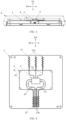
FIG. 1 is a three-dimensional schematic diagram of a structure of a detection apparatus according to a first embodiment of this application, where in the figure, another component is accommodated in space encircled by a radome and a base, and is not shown; -
FIG. 2 is a schematic top view of the structure of the detection apparatus inFIG. 1 in a perspective manner; -
FIG. 3 is a schematic side view of the structure of the detection apparatus inFIG. 1 ; -
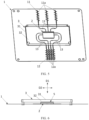
FIG. 4 is a schematic top view of a partial structure of the detection apparatus inFIG. 1 , where relative positions of a wave-absorbing component and a circuit board are shown; -
FIG. 5 is a three-dimensional schematic diagram of the structure shown inFIG. 4 ; -
FIG. 6 is a schematic main view of the structure shown inFIG. 4 ; -
FIG. 7 is a schematic side view of the structure shown inFIG. 4 ; -
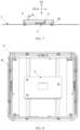
FIG. 8 is a schematic bottom view of a partial structure of a detection apparatus according to a second embodiment of this application; and -
FIG. 9 is a schematic top view of a partial structure of a detection apparatus according to a second embodiment of this application. -
- 1: circuit board; 11: transmit antenna; 11a: transmit antenna module; 12: receive antenna; 12a: receive antenna module; 13: feeder;
- 2: radio frequency chip;
- 3: wave-absorbing component; 31: peripheral structure; 32: wave-absorbing medium;
- 4: radome; 41: wave transmission part;
- 5: heat conducting component;
- D1: first direction; D2: second direction; and D3: third direction.
- The following describes various example embodiments, features, and aspects of this application in detail with reference to the accompanying drawings. Identical reference numerals in the accompanying drawings indicate elements that have same or similar functions. Although various aspects of embodiments are illustrated in the accompanying drawings, the accompanying drawings are not necessarily drawn in proportion unless otherwise specified.
- The specific term "example" herein means "used as an example, embodiment, or illustration". Any embodiment described as "exemplary" is not necessarily explained as being superior or better than other embodiments.
- In addition, to better describe this application, numerous specific details are given in the following specific embodiments. A person skilled in the art should understand that this application can still be implemented without some specific details. In some examples, methods, means, and elements that are well-known to a person skilled in the art are not described in detail, so that the subject matter of this application is highlighted.
- In this application, unless otherwise specified, a "wavelength" of an electromagnetic wave is a medium wavelength of the electromagnetic wave. For example, the medium wavelength may be a wavelength of the electromagnetic wave in a circuit board, but based on an actual situation, the medium wavelength may alternatively be set to a wavelength of the electromagnetic wave in another medium.
- In this application, a "feeder" may be a feed line extending from a radio frequency chip to an antenna module that can receive and transmit an electromagnetic wave, that is, does not include a feeder part that forms the antenna module. The "antenna module" means that a branch on the circuit board is provided with a lead or a cable of an antenna radiation unit. The "antenna radiation unit" is a minimum working unit of a transmit antenna or a receive antenna, and can effectively transmit and receive an electromagnetic wave. In addition, a shape and a size of the feeder are not limited in the solution of this application, and the shape and the size of the feeder in this application may be randomly changed as required.
- In this application, unless otherwise specified, "a first direction D1" is a direction perpendicular to the circuit board, and "a second direction D2" and "a third direction D3" are two directions parallel to the circuit board and perpendicular to each other. In a specific embodiment, the "second direction D2" and the "third direction D3" are separately directions extending from two sides perpendicular to each other in a plane of a square circuit board or two directions perpendicular to each other in a plane of a non-square circuit board. The foregoing directions are defined only for ease of describing a structure of a detection apparatus according to this application, and do not impose any limitation on a usage status of the detection apparatus according to this application. In addition, unless otherwise specified, a "channel" refers to a structure of the detection apparatus for receiving and transmitting an electromagnetic wave.
- The following describes a structure of a detection apparatus according to a first embodiment of this application with reference to the accompanying drawings.
- (Structure of the detection apparatus according to the first embodiment of this application)
- As shown in
FIG. 1 to FIG. 7 , the detection apparatus according to the first embodiment of this application is an in-vehicle continuous wave radar using a millimeter wave, and the detection apparatus includes acircuit board 1, aradio frequency chip 2, a wave-absorbingcomponent 3, and aradome 4. Further, the detection apparatus may further include aheat conducting component 5. - In this embodiment, as shown in
FIG. 4 andFIG. 5 , thecircuit board 1 is a printed circuit board. Theentire circuit board 1 has a square shape, for example, a rectangle or a square. This is not specifically limited in this application. Thecircuit board 1 is provided with a chip installation part for installing theradio frequency chip 2, and the chip installation part may be located in a roughly central part of thecircuit board 1 or in another possible position. Thecircuit board 1 is provided with a transmitantenna 11 and a receiveantenna 12. - In a design, the transmit
antenna 11 includes a plurality of transmitantenna modules 11a arranged in a second direction D2, and the receiveantenna 12 includes a plurality of receiveantenna modules 12a arranged in the second direction D2. In a third direction D3, the transmitantenna 11 and the receiveantenna 12 are located on two sides of the chip installation part. In addition, thecircuit board 1 is further provided with afeeder 13 extending from the chip installation part and connected to each transmitantenna module 11a and each receiveantenna module 12a, and the transmitantenna 11 and the receiveantenna 12 are connected to theradio frequency chip 2 through thefeeder 13. In another design, the plurality of transmitantenna modules 11a of the transmitantenna 11 are staggered in the third direction D3, or the plurality of receiveantenna modules 12a of the receiveantenna 12 are staggered in the third direction D3. In still another design, the transmitantenna 11 may include one transmitantenna module 11a, and the receiveantenna 12 includes one receiveantenna module 12a. In the third direction D3, the transmitantenna 11 and the receiveantenna 12 are located on a same side of the chip installation part. In yet another design, the transmitantenna 11 may include a plurality of transmitantenna modules 11a, and the receiveantenna 12 includes a plurality of receiveantenna modules 12a. The transmitantenna 11 and the receiveantenna 12 may be located on a same side of the chip installation part, and the plurality of transmitantenna modules 11a of the transmitantenna 11 and the plurality of receiveantenna modules 12a of the receiveantenna 12 are alternately arranged in the second direction D2. In other words, an arrangement manner of the transmitantenna 11 and the receiveantenna 12 may be adjusted based on a requirement. This is not limited in the solutions of this application. - It should be noted that the
feeder 13 in this application does not include a feeder part that forms an antenna, but includes a section of feeder that is led out from theradio frequency chip 2. For example, thefeeder 13 is shown inFIG. 4 andFIG. 5 . In addition, in actual implementation, various components, such as an antenna, a feeder, and a radio frequency chip, disposed on thecircuit board 1 may have a plurality of design manners, andfeeders 13 corresponding to these design manners may have different shapes and sizes. A specific component of thefeeder 13 is not limited herein. - In this embodiment, as shown in
FIG. 4 andFIG. 5 , the radio frequency chip 2 (for example, a monolithic microwave integrated circuit MMIC) is installed on the chip installation part of thecircuit board 1, and theradio frequency chip 2 is connected to each transmitantenna module 11a and each receiveantenna module 12a through thefeeder 13 disposed on thecircuit board 1. In this way, theradio frequency chip 2 cooperates with the transmitantenna 11 and the receiveantenna 12 to implement conversion between an electromagnetic wave (for example, a millimeter wave) transmitted in space and an intra-board high-frequency current, and identify corresponding information. - In this embodiment, as shown in
FIG. 3 ,FIG. 6 , andFIG. 7 , the wave-absorbingcomponent 3 and theradio frequency chip 2 are located on a same side of thecircuit board 1, and the wave-absorbingcomponent 3 is located above the circuit board, and is configured to absorb leaked energy, to improve isolation between channels, thereby reducing interference between the channels. The wave-absorbingcomponent 3 includes aperipheral structure 31 and a wave-absorbingmedium 32 accommodated in theperipheral structure 31, and the wave-absorbingmedium 32 fills internal space of theperipheral structure 31. The wave-absorbingcomponent 3 is installed and fastened to a part that is of thecircuit board 1 and on which theradio frequency chip 2 is disposed. As shown inFIG. 4 andFIG. 5 , the wave-absorbingcomponent 3 is located between the transmitantenna 11 and the receiveantenna 12, so that the transmitantenna 11 and the receiveantenna 12 are located on two sides of the wave-absorbingcomponent 3. Optionally, in a design, when the transmitantenna 11 and the receiveantenna 12 are located on a same side of the chip installation part, a part of the wave-absorbingcomponent 3 may be located between the transmitantenna 11 and the receiveantenna 12. - As shown in
FIG. 4 andFIG. 5 , when observation is performed in a first direction D1 perpendicular to thecircuit board 1, the wave-absorbingcomponent 3 completely covers theradio frequency chip 2; and when observation is performed in the first direction D1, the wave-absorbingcomponent 3 covers a part of thefeeder 13. In this way, the wave-absorbingcomponent 3 can effectively shield theradio frequency chip 2 and thefeeder 13, to absorb energy leaked from theradio frequency chip 2 and thefeeder 13. In this application, "covering" may be a case in which the wave-absorbingcomponent 3 shields theradio frequency chip 2 from a side (an upper part inFIG. 3 ,FIG. 6 , andFIG. 7 ) of the first direction D1, or a case in which the wave-absorbingcomponent 3 half-encircles theradio frequency chip 2 and thefeeder 13 from an upper part and a side. - In this embodiment, as shown in
FIG. 3 to FIG. 7 , a shape of theperipheral structure 31 is a cuboid or an approximate cuboid, and a shape of the space used to accommodate the wave-absorbingmedium 32 inside theperipheral structure 31 is a cuboid or an approximate cuboid that is geometrically similar to the shape outside. In an optional design, a thickness direction of theperipheral structure 31 is consistent with thefirst direction D 1, a length direction is consistent with the second direction D2, and a width direction is consistent with the third direction D3. In another design, the length direction and the width direction are perpendicular to each other, and may have a specific angle with the second direction and the third direction respectively. In a further optional design, a fastening hole corresponding to a fastening hole of thecircuit board 1 is formed at each of four corners of theperipheral structure 31, and theperipheral structure 31 is fastened to thecircuit board 1 through a fastening post that passes through the fastening hole of theperipheral structure 31 and the fastening hole of the circuit board 1 (as shown inFIG. 6 andFIG. 7 ). - Because a main component of the wave-absorbing
medium 32 is water, to ensure that theperipheral structure 31 has high enough sealing performance, theperipheral structure 31 may be made of a hydrophobic material, and an inner surface of theperipheral structure 31 may undergo hydrophobic treatment. The hydrophobic material includes at least one of the following materials: nitrile-butadiene rubber, polytetrafluoroethylene, and silicon dioxide. For hydrophobic treatment, a P2i nanomaterial process can be used. In the P2i nanomaterial process, a pulsed ionized gas (plasma) generated in a vacuum chamber is used to apply a perfluorocarbon polymer to the inner surface or a whole surface of the entireperipheral structure 31. The P2i nanomaterial process significantly reduces surface energy. Therefore, when the inner surface of theperipheral structure 31 is in contact with liquid, the liquid becomes a bead-like body and cannot penetrate the inner surface. In this way, water cannot penetrate theperipheral structure 31 or be absorbed by theperipheral structure 31, and can be sealed inside theperipheral structure 31 for a long time. While ensuring the sealing performance, theperipheral structure 31 forms as much space as possible inside theperipheral structure 31 to accommodate the wave-absorbingmedium 32. - Specifically, the wave-absorbing medium may be only water, or the wave-absorbing
medium 32 may be a mixed solution of water and ethylene glycol. Water has characteristics of a high dielectric constant and a high loss angle tangent for an electromagnetic wave, and can effectively absorb and consume unrelated energy leaked by theradio frequency chip 2, thefeeder 13, and the transmitantenna 11, so that the unrelated energy is weakened or even disappears. Ethylene glycol, as an antifreeze, is mixed with water at a predetermined mass percentage concentration, which can effectively reduce a freezing point of the wave-absorbingmedium 32 and support the apparatus to work in a low-temperature environment. In addition, the wave-absorbingmedium 32 using the mixed solution of water and ethylene glycol can improve heat dissipation performance of theradio frequency chip 2. - Further, an experiment shows that, if a length, width, or thickness of the wave-absorbing
component 3 is insufficient, energy attenuation is insufficient, which causes interference to a channel of the detection apparatus. To effectively improve isolation between channels by using the wave-absorbingcomponent 3, the wave-absorbing component 3 (mainly referring to the peripheral structure 31) should meet a predetermined three-dimensional size requirement. - Specifically, in the second direction D2, the wave-absorbing
component 3 extends beyond two ends of the transmitantenna 11 and extends beyond two ends of the receiveantenna 12. Considering that a shape and a size of the wave-absorbingmedium 32 are limited by using theperipheral structure 31, on any side in the second direction D2, the inner surface (that is, an outer surface of the wave-absorbing medium 32) of theperipheral structure 31 extends beyond a boundary of theradio frequency chip 2 or thefeeder 13. Optionally, a length that is of the inner surface (that is, the outer surface of the wave-absorbing medium 32) of theperipheral structure 31 and that extends beyond the boundary of theradio frequency chip 2 or thefeeder 13 is greater than or equal to twice a medium wavelength. In this embodiment, correspondingly, a length that is of the inner surface (that is, the outer surface of the wave-absorbing medium 32) of theperipheral structure 31 and that extends beyond one of theradio frequency chip 2 and thefeeder 13 that is closer to the outside in the second direction is greater than or equal to twice the medium wavelength. In this way, the wave-absorbingcomponent 3 has a sufficient length. That is, as shown inFIG. 4 , in the second direction D2, with the left side used as an example, both a part that is of thefeeder 13 and that is connected to the transmitantenna 11 and a part that is of thefeeder 13 and that is connected to the receiveantenna 12 are closer to the left side than theradio frequency chip 2, that is, thefeeder 13 is closer to the outside than theradio frequency chip 2 on the left side. Correspondingly, on the left side of the second direction D2, a size of a part that is of the left side of the outer surface of the wave-absorbingmedium 32 and that exceeds a leftmost part of the feeder 13 (the part is a boundary of thefeeder 13 on the left side) is greater than or equal to twice a wavelength of an electromagnetic wave transmitted by the detection apparatus. The foregoing size condition is also met on the right side of the second direction D2. To avoid affecting normal operation of the transmitantenna 11 and the receiveantenna 12, the wave-absorbingcomponent 3 cannot cover the transmitantenna 11 and the receiveantenna 12. Therefore, in the third direction D3, a width of theperipheral structure 31 should not be greater than a minimum spacing between the transmitantenna 11 and the receiveantenna 12, and on this basis, the width of theperipheral structure 31 should be as large as possible, so that the wave-absorbing medium has a sufficient width to cover afeeder 13 of a sufficient size. In a variant design of the foregoing embodiment, the transmitantenna 11 and the receiveantenna 12 are located on two sides of the wave-absorbingcomponent 3 in the second direction D2, and on any side of the third direction D3, the inner surface (that is, the outer surface of the wave-absorbing medium 32) of theperipheral structure 31 may extend the boundary of theradio frequency chip 2 or thefeeder 13. Optionally, a width that is of the inner surface (that is, the outer surface of the wave-absorbing medium 32) of theperipheral structure 31 and that extends beyond the boundary of theradio frequency chip 2 or thefeeder 13 is greater than or equal to twice the medium wavelength. In the variant design, it may be understood that, the width that is of the inner surface (that is, the outer surface of the wave-absorbing medium 32) of theperipheral structure 31 and that extends beyond one of theradio frequency chip 2 and thefeeder 13 that is closer to the outside is greater than or equal to twice the wavelength of the electromagnetic wave transmitted by the detection apparatus. For the size condition herein, refer to the foregoing explanation described in the foregoing embodiment. Further, optionally, in the first direction D1, a minimum thickness of the wave-absorbingmedium 32 is greater than or equal to 1/2 of the wavelength of the electromagnetic wave transmitted by the detection apparatus. Further, optionally, in thefirst direction D 1, a maximum distance between outer surfaces that are of the wave-absorbingmedium 32 and thecircuit board 1 and that face each other is less than or equal to 1/4 of the wavelength. That is, in this embodiment, as shown inFIG. 3 ,FIG. 6 , andFIG. 7 , in the first direction D1, a maximum distance between a lower surface of the wave-absorbingmedium 32 and an upper surface of thecircuit board 1 is less than or equal to 1/4 of the wavelength. According to the foregoing size design, the wave-absorbingcomponent 3 has effect of "a barrier wall", thereby effectively attenuating leaked energy and improving isolation between channels. - In this embodiment, as shown in
FIG. 1 to FIG. 3 , theradome 4 is configured to cover thecircuit board 1 and theradio frequency chip 2, the wave-absorbingcomponent 3, and the like disposed on thecircuit board 1. - In this embodiment, as shown in
FIG. 3 ,FIG. 6 , andFIG. 7 , theheat conducting component 5 is disposed between theradio frequency chip 2 and the wave-absorbingcomponent 3, and theheat conducting component 5 is in direct contact with theradio frequency chip 2, so that heat generated by theradio frequency chip 2 can be transferred to the wave-absorbingcomponent 3 through theheat conducting component 5. Specifically, theheat conducting component 5 includes a steel sheet and a heat conducting gel. The steel sheet is embedded into a part that is of theperipheral structure 31 and that is in contact with theradio frequency chip 2 in an in-film injection molding manner. The heat conducting gel is added between the steel sheet and theradio frequency chip 2. Theheat conducting component 5 can significantly improve a heat dissipation capability of theradio frequency chip 2. In addition, the steel sheet further improves rigidity of the wave-absorbingcomponent 3 at a part corresponding to theradio frequency chip 2. In this way, when the detection apparatus is under unexpected pressure, the steel sheet can prevent theradio frequency chip 2 from being affected by the unexpected pressure. - The following describes a structure of a detection apparatus according to a second embodiment of this application with reference to the accompanying drawings.
- The structure of the detection apparatus according to the second embodiment of this application is basically the same as the structure of the detection apparatus according to the first embodiment of this application. The following describes a difference between the two.
- In this embodiment, as shown in
FIG. 8 andFIG. 9 , the wave-absorbingcomponent 3 is fastened to theradome 4. Specifically, the wave-absorbingcomponent 3 may be independently formed and fastened to theradome 4, or the wave-absorbingcomponent 3 may be integrated with another part of theradome 4. In this embodiment, the wave-absorbingcomponent 3 also covers theradio frequency chip 2 and thefeeder 13, and is located between the transmitantenna 11 and the receiveantenna 12. In addition, except for a part used to fasten the wave-absorbingcomponent 3, the other part of theradome 4 is used as awave transmission part 41. An electromagnetic wave can be transmitted through thewave transmission part 41, and an electromagnetic wave from the outside can be received through thewave transmission part 41, so that normal operation of the detection apparatus is not affected. - The foregoing describes the example embodiments of this application, and the following provides supplementary descriptions.
- i. Although no specific description is provided in the specific implementation, it should be understood that the
circuit board 1 may be provided with a plurality of receive antennas and a plurality of transmit antennas. The wave-absorbingcomponent 3 may not form a cuboid shape, but form a special shape based on a requirement, so that a part of the wave-absorbing component may be located between two adjacent receive antennas, and the other part of the wave-absorbing component may be located between two adjacent transmit antennas. - ii. Although it is described in the specific implementation that the
peripheral structure 31 is fastened to thecircuit board 1 in a manner of being spaced away from thecircuit board 1, this application is not limited thereto. For example, the following technical solution may be used.
A concave part that accommodates theradio frequency chip 2 is formed at a part that is of theperipheral structure 31 and that corresponds to theradio frequency chip 2, and a specific interval is further formed between theperipheral structure 31 and thefeeder 13. Further, a gapless "zero fitting" is used between theperipheral structure 31 and a part of thecircuit board 1 except theradio frequency chip 2 and thefeeder 13, to suppress a surface wave excited by the transmitantenna 11 on thecircuit board 1. In this case, in order not to affect normal operation of thefeeder 13, the transmitantenna 11, and the receiveantenna 12, the wave-absorbingcomponent 3 is spaced from a part that is of thecircuit board 1 and at which thefeeder 13 is formed, and is spaced from antenna radiation units of the transmitantenna 11 and the receiveantenna 12. The antenna radiation unit is a minimum working unit of the transmitantenna 11 or the receiveantenna 12, and can effectively transmit and receive an electromagnetic wave. - iii. Although not explicitly stated in the specific embodiment, it should be understood that the mass percentage concentration between the ethylene glycol and the water in the wave-absorbing
medium 32 may be adjusted as required. A test shows that when the mass percentage concentration of the ethylene glycol in the wave-absorbingmedium 32 is 54%, an ice point of the wave-absorbingmedium 32 is -40 degrees Celsius; and when the mass percentage concentration of the ethylene glycol in the wave-absorbingmedium 32 is 60%, the ice point of the wave-absorbingmedium 32 is -48.3 degrees Celsius. In an optional design, the mass percentage concentration of the ethylene glycol in the wave-absorbingmedium 32 is not greater than 60%. In this way, ethylene glycol mixture in the wave-absorbingmedium 32 does not freeze in a low temperature environment, and the wave-absorbingmedium 32 can still maintain a liquid state and maintain absorption effect on an electromagnetic wave. In addition, in some environments where temperature is not lower than zero degrees, the wave-absorbingmedium 32 may be made up of water and does not include ethylene glycol. - iv. Although it is described in the specific implementation that the transmit
antenna 11 and the receiveantenna 12 are disposed on two sides of theradio frequency chip 2, this application is not limited thereto. For example, the transmitantenna 11 and the receiveantenna 12 may be disposed on a same side of theradio frequency chip 2. In this case, the wave-absorbingcomponent 3 may use another shape and structure, to cover theradio frequency chip 2 and thefeeder 13 and be disposed between the transmitantenna 11 and the receiveantenna 12. - v. In this application, the following beneficial effect may be obtained by using the technical solutions of this application:
- (1) Water is used as the wave-absorbing medium to effectively absorb energy leaked by the radio frequency chip and the feeder, improve isolation between the transmit channels, the receive channels, and the receive channel and the transmit channel of the detection apparatus, prevent antenna pattern distortion, reduce interference to the receive channel and the transmit channel, ensure a receiver sensitivity and noise figure, and improve competitiveness of the entire system.
- (2) The detection apparatus is highly compatible with antenna design solutions, and can be adjusted based on different antenna solutions, to be quickly iterated and optimized with little impact on the antenna performance and radiation pattern.
- (3) Low-cost and easy-to-obtain water is used as a wave-absorbing material, thereby reducing dependence on a specific wave-absorbing material, and wave-absorbing effect is obvious. The water further has good heat dissipation and cooling effect on the
radio frequency chip 2, and allows the chip to work in a higher wave-transmitting duty cycle state, thereby improving a detection signal-to-noise ratio. - (4) A material selected for the
peripheral structure 31 of the wave-absorbingassembly 3 has a thermoplastic attribute, can be manufactured in batches by opening a mold, and has low assembly costs, and is suitable for batch assembly and production in a production line. - (5) The structure of a wave absorption area is simple, an area is small, and is conducive for system integration.
- vi. Not explicitly described in the foregoing specific implementation, this application further provides a millimeter-wave radar, including the detection apparatus described in various embodiments described in the foregoing specific implementation.
- Further, this application further provides a terminal device, including the detection apparatus described in the foregoing embodiments described in the specific implementations. Further, the terminal device may be an intelligent transportation device (for example, an auto-driving system and a road monitoring system), a smart home device, an intelligent manufacturing device, an uncrewed aerial vehicle, or a robot, but is not limited to the foregoing device and machine. Instead, the detection apparatus in this application may be applied to various other devices based on a requirement.
- Although this application is described with reference to embodiments, in a process of implementing this application that claims protection, a person skilled in the art may understand and implement another variation of the disclosed embodiments by viewing the accompanying drawings, disclosed content, and the accompanying claims. In the claims, "comprising" does not exclude another component or another step, and "a" or "one" does not exclude a meaning of plurality. Some measures are recorded in dependent claims that are different from each other, but this does not mean that these measures cannot be combined to produce a better effect.
- Embodiments of this application are described above. The foregoing descriptions are examples, not exhaustive, and not limited to the foregoing disclosed embodiments. Many modifications and variations are apparent to a person of ordinary skill in the art without departing from the scope and spirit of the described embodiments. Selection of terms used in this specification is intended to best explain embodiment principles, actual application or improvements to technologies in the market, or to enable another person of ordinary skill in the art to understand the embodiments disclosed in this specification.
Claims (23)
- A detection apparatus, comprising a circuit board and a radio frequency chip, wherein the radio frequency chip is installed on the circuit board, the circuit board is provided with a transmit antenna, a receive antenna, and a feeder, and the transmit antenna and the receive antenna are connected to the radio frequency chip through the feeder, whereinthe detection apparatus further comprises a wave-absorbing component, wherein the wave-absorbing component and the radio frequency chip are located on a same side of the circuit board;in a first direction perpendicular to the circuit board, the wave-absorbing component covers the radio frequency chip; andthe wave-absorbing component comprises a peripheral structure and a wave-absorbing medium encircled and accommodated by the peripheral structure, and the wave-absorbing medium comprises water.
- The detection apparatus according to claim 1, wherein in the first direction, the wave-absorbing component covers a part or all of the feeder.
- The detection apparatus according to claim 1 or 2, wherein in the first direction, a minimum thickness of the wave-absorbing medium is greater than or equal to 1/2 of a medium wavelength, and the medium wavelength is a wavelength that is of an electromagnetic wave transmitted by the detection apparatus and that is in the circuit board.
- The detection apparatus according to any one of claims 1 to 3, wherein in the first direction, a maximum distance between outer surfaces that are of the wave-absorbing medium and the circuit board and that face each other is less than or equal to 1/4 of the medium wavelength.
- The detection apparatus according to any one of claims 1 to 4, whereinon any side in a second direction, the outer surface of the wave-absorbing medium exceeds a boundary of the radio frequency chip or the feeder; and/oron any side in a third direction, the outer surface of the wave-absorbing medium exceeds the boundary of the radio frequency chip or the feeder, whereinthe second direction and the third direction are parallel to the circuit board, and the second direction is perpendicular to the third direction.
- The detection apparatus according to any one of claims 1 to 5, wherein the wave-absorbing component is located between the receive antenna and the transmit antenna.
- The detection apparatus according to any one of claims 1 to 6, wherein the circuit board comprises a plurality of receive antennas and a plurality of transmit antennas;a part of the wave-absorbing component is located between two adjacent receive antennas; and/ora part of the wave-absorbing component is located between two adjacent transmit antennas.
- The detection apparatus according to any one of claims 1 to 7, wherein the peripheral structure is made of a hydrophobic material.
- The detection apparatus according to claim 8, wherein the hydrophobic material comprises at least one of the following materials: nitrile-butadiene rubber, polytetrafluoroethylene, and silicon dioxide.
- The detection apparatus according to any one of claims 1 to 9, wherein an inner surface of the peripheral structure undergoes hydrophobic treatment.
- The detection apparatus according to any one of claims 1 to 10, wherein the wave-absorbing medium further comprises ethylene glycol.
- The detection apparatus according to any one of claims 1 to 11, wherein the detection apparatus further comprises a heat conducting component, the heat conducting component is disposed between the wave-absorbing component and the radio frequency chip, and the heat conducting component is in contact with the radio frequency chip.
- The detection apparatus according to claim 12, wherein the heat conducting component comprises at least one of a metal sheet and a heat conducting medium.
- The detection apparatus according to any one of claims 1 to 13, wherein the detection apparatus is a millimeter-wave detection apparatus.
- A radome, wherein the radome comprises a wave-absorbing component, the wave-absorbing component comprises a peripheral structure and a wave-absorbing medium accommodated by the peripheral structure, and the wave-absorbing medium comprises water.
- The radome according to claim 15, wherein the radome further comprises a wave transmission part, and the wave-absorbing component and the wave transmission part are installed in a fastened manner.
- The radome according to claim 15 or 16, wherein the peripheral structure is made of a hydrophobic material.
- The radome according to claim 17, wherein the hydrophobic material comprises at least one of the following materials: nitrile-butadiene rubber, polytetrafluoroethylene, and silicon dioxide.
- The radome according to any one of claims 15 to 18, wherein an inner surface of the peripheral structure undergoes hydrophobic treatment.
- The radome according to any one of claims 15 to 19, wherein the wave-absorbing medium further comprises ethylene glycol.
- A millimeter-wave radar, wherein the millimeter-wave radar comprises the detection apparatus according to any one of claims 1 to 14, or comprises the radome according to any one of claims 15 to 20.
- A terminal device, wherein the terminal device comprises the detection apparatus according to any one of claims 1 to 14, or comprises the radome according to any one of claims 15 to 20.
- The terminal device according to claim 22, wherein the terminal device is an intelligent transportation device, a smart home device, an intelligent manufacturing device, an uncrewed aerial vehicle, or a robot.
Applications Claiming Priority (2)
| Application Number | Priority Date | Filing Date | Title |
|---|---|---|---|
| CN202110405826.6A CN115224485A (en) | 2021-04-15 | 2021-04-15 | Detection device, antenna housing, millimeter wave radar and terminal equipment |
| PCT/CN2022/086119 WO2022218258A1 (en) | 2021-04-15 | 2022-04-11 | Detection apparatus, radome, millimeter-wave radar and terminal device |
Publications (2)
| Publication Number | Publication Date |
|---|---|
| EP4325663A1 true EP4325663A1 (en) | 2024-02-21 |
| EP4325663A4 EP4325663A4 (en) | 2024-10-09 |
Family
ID=83605397
Family Applications (1)
| Application Number | Title | Priority Date | Filing Date |
|---|---|---|---|
| EP22787484.9A Pending EP4325663A4 (en) | 2021-04-15 | 2022-04-11 | DETECTION DEVICE, RADOME, MILLIMETER WAVE RADAR AND TERMINAL DEVICE |
Country Status (3)
| Country | Link |
|---|---|
| EP (1) | EP4325663A4 (en) |
| CN (1) | CN115224485A (en) |
| WO (1) | WO2022218258A1 (en) |
Family Cites Families (11)
| Publication number | Priority date | Publication date | Assignee | Title |
|---|---|---|---|---|
| US3325808A (en) * | 1965-09-07 | 1967-06-13 | North American Aviation Inc | Electromagnetic energy attenuator |
| JP2004140632A (en) * | 2002-10-18 | 2004-05-13 | Hitachi Ltd | High frequency transmitting / receiving device and method of manufacturing the same |
| JP2007074662A (en) * | 2005-09-09 | 2007-03-22 | Hitachi Ltd | Millimeter wave radar equipment |
| JP2010210297A (en) * | 2009-03-09 | 2010-09-24 | Furukawa Electric Co Ltd:The | Wide coverage radar apparatus |
| US9208913B2 (en) * | 2011-03-31 | 2015-12-08 | Kuang-Chi Innovative Technology Ltd. | Wave-absorbing metamaterial |
| DE102019200912A1 (en) * | 2019-01-24 | 2020-07-30 | Robert Bosch Gmbh | Radome assembly for a radar sensor for motor vehicles |
| CN112398497A (en) * | 2019-08-16 | 2021-02-23 | 华为技术有限公司 | Radio frequency device and assembling method thereof |
| CN110797664A (en) * | 2019-11-11 | 2020-02-14 | 上海电力大学 | Adjustable coding basic unit with dual functions and super surface |
| CN212209738U (en) * | 2020-05-25 | 2020-12-22 | 上海载德信息科技股份有限公司 | Millimeter wave radar |
| CN111900548B (en) * | 2020-08-28 | 2021-06-25 | 西安电子科技大学 | Ultra-Broadband Low Scattering Metamaterial Based on Combination of Absorber and Metasurface |
| CN112271461B (en) * | 2020-10-27 | 2021-07-02 | 华中科技大学 | A Hybrid Loaded Dual Polarization Ground Penetrating Radar Array Antenna |
-
2021
- 2021-04-15 CN CN202110405826.6A patent/CN115224485A/en active Pending
-
2022
- 2022-04-11 EP EP22787484.9A patent/EP4325663A4/en active Pending
- 2022-04-11 WO PCT/CN2022/086119 patent/WO2022218258A1/en not_active Ceased
Also Published As
| Publication number | Publication date |
|---|---|
| CN115224485A (en) | 2022-10-21 |
| WO2022218258A1 (en) | 2022-10-20 |
| EP4325663A4 (en) | 2024-10-09 |
Similar Documents
| Publication | Publication Date | Title |
|---|---|---|
| EP2221910B1 (en) | Base station RF duplexer, RF module, and RF system field | |
| KR20180089302A (en) | Radio frequency device packages and methods of formation thereof | |
| CN113161720B (en) | Antenna, base station and terminal with high isolation and low cross polarization level | |
| EP3772131A1 (en) | Antenna device and electronic device | |
| CN111446550B (en) | Wave absorbing structure, antenna module and electronic equipment | |
| WO2015127876A1 (en) | Dual-polarized antenna and antenna array | |
| WO2020233478A1 (en) | Antenna unit and terminal device | |
| EP4016854A1 (en) | Radio frequency device and assembling method therefor | |
| WO2023273896A1 (en) | Antenna and base station | |
| CN217281195U (en) | Millimeter wave radio frequency module and electronic equipment | |
| CN110996496B (en) | Circuit board, antenna assembly and dual polarized antenna | |
| CN115863974B (en) | Energy selection antenna and design method thereof | |
| EP3965538A1 (en) | Housing assembly, antenna apparatus and electronic device | |
| CN209329147U (en) | A kind of four unit MIMO hand held antenna system of compact | |
| CN212162084U (en) | Device for improving receiving and transmitting isolation of traffic radar antenna and traffic radar signal receiving and transmitting device | |
| WO2022218258A1 (en) | Detection apparatus, radome, millimeter-wave radar and terminal device | |
| CN107331950B (en) | Circular 4G LTE MIMO vehicle antenna | |
| CN114792882B (en) | Millimeter wave radio frequency module and electronic equipment | |
| CN211240266U (en) | Circuit board, antenna assembly and dual polarized antenna | |
| CN220042284U (en) | Antenna and vehicle | |
| WO2024027465A1 (en) | Antenna system and base station | |
| CN215266654U (en) | Waveguide antenna unit and waveguide array antenna | |
| US20260066547A1 (en) | Antenna structure and communication device | |
| CN216253330U (en) | Receiving and transmitting shielding structure between waveguide and circuit board | |
| CN218632452U (en) | GNSS and 5G hybrid antenna |
Legal Events
| Date | Code | Title | Description |
|---|---|---|---|
| STAA | Information on the status of an ep patent application or granted ep patent |
Free format text: STATUS: THE INTERNATIONAL PUBLICATION HAS BEEN MADE |
|
| PUAI | Public reference made under article 153(3) epc to a published international application that has entered the european phase |
Free format text: ORIGINAL CODE: 0009012 |
|
| STAA | Information on the status of an ep patent application or granted ep patent |
Free format text: STATUS: REQUEST FOR EXAMINATION WAS MADE |
|
| 17P | Request for examination filed |
Effective date: 20231114 |
|
| AK | Designated contracting states |
Kind code of ref document: A1 Designated state(s): AL AT BE BG CH CY CZ DE DK EE ES FI FR GB GR HR HU IE IS IT LI LT LU LV MC MK MT NL NO PL PT RO RS SE SI SK SM TR |
|
| DAV | Request for validation of the european patent (deleted) | ||
| DAX | Request for extension of the european patent (deleted) | ||
| REG | Reference to a national code |
Ref country code: DE Ref legal event code: R079 Free format text: PREVIOUS MAIN CLASS: H01Q0001520000 Ipc: G01S0007030000 |
|
| A4 | Supplementary search report drawn up and despatched |
Effective date: 20240905 |
|
| RIC1 | Information provided on ipc code assigned before grant |
Ipc: H01Q 11/04 20060101ALI20240830BHEP Ipc: H01Q 1/32 20060101ALI20240830BHEP Ipc: H01Q 17/00 20060101ALI20240830BHEP Ipc: H01Q 1/52 20060101ALI20240830BHEP Ipc: G01S 7/03 20060101AFI20240830BHEP |
|
| RAP1 | Party data changed (applicant data changed or rights of an application transferred) |
Owner name: SHENZHEN YINWANG INTELLIGENTTECHNOLOGIES CO., LTD. |