EP4325576A1 - Semiconductor device forming method and semiconductor device - Google Patents
Semiconductor device forming method and semiconductor device Download PDFInfo
- Publication number
- EP4325576A1 EP4325576A1 EP22918042.7A EP22918042A EP4325576A1 EP 4325576 A1 EP4325576 A1 EP 4325576A1 EP 22918042 A EP22918042 A EP 22918042A EP 4325576 A1 EP4325576 A1 EP 4325576A1
- Authority
- EP
- European Patent Office
- Prior art keywords
- word line
- forming
- layers
- transistors
- dielectric
- Prior art date
- Legal status (The legal status is an assumption and is not a legal conclusion. Google has not performed a legal analysis and makes no representation as to the accuracy of the status listed.)
- Pending
Links
Images







Classifications
-
- H—ELECTRICITY
- H10—SEMICONDUCTOR DEVICES; ELECTRIC SOLID-STATE DEVICES NOT OTHERWISE PROVIDED FOR
- H10B—ELECTRONIC MEMORY DEVICES
- H10B12/00—Dynamic random access memory [DRAM] devices
- H10B12/30—DRAM devices comprising one-transistor - one-capacitor [1T-1C] memory cells
-
- H—ELECTRICITY
- H10—SEMICONDUCTOR DEVICES; ELECTRIC SOLID-STATE DEVICES NOT OTHERWISE PROVIDED FOR
- H10B—ELECTRONIC MEMORY DEVICES
- H10B12/00—Dynamic random access memory [DRAM] devices
- H10B12/30—DRAM devices comprising one-transistor - one-capacitor [1T-1C] memory cells
- H10B12/48—Data lines or contacts therefor
- H10B12/482—Bit lines
-
- H—ELECTRICITY
- H10—SEMICONDUCTOR DEVICES; ELECTRIC SOLID-STATE DEVICES NOT OTHERWISE PROVIDED FOR
- H10B—ELECTRONIC MEMORY DEVICES
- H10B12/00—Dynamic random access memory [DRAM] devices
- H10B12/01—Manufacture or treatment
- H10B12/02—Manufacture or treatment for one transistor one-capacitor [1T-1C] memory cells
- H10B12/03—Making the capacitor or connections thereto
-
- H—ELECTRICITY
- H10—SEMICONDUCTOR DEVICES; ELECTRIC SOLID-STATE DEVICES NOT OTHERWISE PROVIDED FOR
- H10B—ELECTRONIC MEMORY DEVICES
- H10B12/00—Dynamic random access memory [DRAM] devices
- H10B12/30—DRAM devices comprising one-transistor - one-capacitor [1T-1C] memory cells
- H10B12/48—Data lines or contacts therefor
- H10B12/488—Word lines
-
- H—ELECTRICITY
- H10—SEMICONDUCTOR DEVICES; ELECTRIC SOLID-STATE DEVICES NOT OTHERWISE PROVIDED FOR
- H10D—INORGANIC ELECTRIC SEMICONDUCTOR DEVICES
- H10D62/00—Semiconductor bodies, or regions thereof, of devices having potential barriers
- H10D62/10—Shapes, relative sizes or dispositions of the regions of the semiconductor bodies; Shapes of the semiconductor bodies
- H10D62/113—Isolations within a component, i.e. internal isolations
- H10D62/115—Dielectric isolations, e.g. air gaps
Definitions
- the embodiments of the disclosure relate to the technical field of semiconductor, and relate to but are not limited to a method for forming a semiconductor device and a semiconductor device.
- DRAM Dynamic Random Access Memory
- embodiments of the disclosure provide a method for forming a semiconductor device and a semiconductor device.
- the embodiments of the disclosure provide a method for forming a semiconductor device.
- the method includes following operations.
- the stacked structure includes alternately stacked dielectric layers and sacrificial layers.
- Multiple isolation layers extending in a first direction and arranged in a second direction are formed in the stacked structure.
- the first direction is perpendicular to the substrate surface.
- the second direction is perpendicular to the first direction
- a bit line is formed between two adjacent ones of the isolation layers.
- the sacrificial layers are removed.
- Capacitor via holes along a third direction is formed in vacancies of a dielectric structure.
- the dielectric structure is formed after removing the sacrificial layers.
- the third direction, the first direction and the second direction are perpendicular to each other.
- Transistors and capacitors are formed sequentially in capacitor via holes based on bit lines.
- the capacitors are parallel to the substrate surface.
- a word line extending in the second direction is formed between two adjacent ones of the transistors to form the semiconductor device.
- the operation that multiple isolation layers extending in a first direction and arranged in a second direction are formed in the stacked structure includes following operations.
- the stacked structure is etched along the first direction to form multiple isolation trenches arranged at an equal interval along the second direction.
- the isolation trenches are filled with an isolation material, to form the multiple isolation layers arranged at an equal interval along the second direction.
- the dielectric structure is formed after removing the sacrificial layers.
- a projection of the dielectric structure in the third direction is grid-shaped.
- the vacancies in the dielectric structure constitute growth regions for the transistors and the capacitors.
- the operation that a bit line is formed between two adjacent ones of the isolation layers includes the following operations.
- a bit via hole is formed between two adjacent ones of the isolation layers.
- the diameter of the bit via hole is greater than or equal to the interval between two adjacent ones of the isolation layers.
- a bit line is formed in bit line via hole. In the first direction, the top surface of the bit line is flush with the top surface of the stacked structure.
- the operation that a bit line via is formed between two adjacent ones of the isolation layers includes following operation.
- the stacked structure is etched in the first direction between two adjacent ones of the isolation layers until the substrate is exposed, to correspondingly form the bit line via hole.
- the operation that transistors and capacitors are sequentially formed in the capacitor via holes based on the bit lines includes the following operations.
- the transistors are formed in the capacitor via holes in the third direction by an epitaxial growth process based on the bit lines.
- the sources of the transistors are connected with the bit lines.
- First electrode layers are formed on inner walls of the capacitor via holes and surfaces of the transistors in the third direction.
- Dielectric layers covering the first electrode layers and second electrode layers covering the dielectric layers are sequentially formed to form the capacitors.
- the operation that a word line extending in the second direction is formed between two adjacent ones of the transistors includes the following operations.
- a word line via hole extending in the second direction is formed in each of the dielectric layers at a position between two adjacent ones of the transistors.
- a gate oxide layer covering a lower surface of each of word line via holes is formed in the first direction.
- Each of the word line via holes having the gate oxide layer is filled to form first initial word lines.
- Each of the first initial word lines is etched back to form a word line combination.
- the word line combination is arranged in a stepped shape at both ends along the first direction.
- the word line combination includes at least two word lines.
- the operation that each of the first initial word lines is etched back includes the following operation.
- the first initial word lines are etched back at least once.
- the operation that a word line extending in the second direction is formed between two adjacent ones of the transistors includes the following operations.
- a word line via hole extending in the second direction is formed in each of the dielectric layers at a position between two adjacent ones of the transistors.
- Each of the word line via holes is filled with a first filling material with a partial depth. Multiple word line via holes with a remaining depth form multiple stepped word line via holes. The multiple stepped word line via holes at one end along the first direction are arranged in a stepped shape.
- Each stepped word line via hole is filled to form a second initial word line combination with one end arranged in the stepped shape.
- the second initial word line combination includes at least two second initial word lines.
- Each of the second initial word lines is etched back to form a word line combination with both ends along the first direction arranged in the stepped shape.
- the word line combination includes at least two word lines.
- the method further includes the following operation.
- a second filling material is filled in the remaining holes left after etching back.
- the upper surface of the second filling material and the outer surface of the dielectric structure are flush.
- the method further includes the following operations.
- the dielectric structure is etched along the first direction at positions corresponding to both ends of each word line to form at least one connecting via hole.
- the connecting via hole exposes a corresponding word lines.
- the connecting via holes are filled to form connecting lines.
- Each word line is connected with two connecting lines.
- the method further includes the following operation.
- An oxide layer covering the stacked structure is formed.
- the oxide layer is connected to an uppermost sacrificial layer in the stacked structure;
- the operation that multiple isolation layers extending in the first direction and arranged in the second direction are formed in the stacked structure includes the following operation.
- the multiple isolation layers extending in the first direction and arranged at equal interval in the second direction are formed in the stacked structure and the oxide layer.
- the embodiments of the disclosure provide a semiconductor device.
- the semiconductor device includes a substrate, a dielectric structure, bit lines, transistors, capacitors and word lines.
- the dielectric structure includes multiple dielectric layers parallel to the substrate and multiple isolation layers perpendicular to the substrate.
- a projection of the dielectric structure in a third direction is grid-shaped.
- bit lines are perpendicular to the substrate and located in the dielectric structure.
- the transistors are parallel to the substrate, connected to the bit lines, located in vacancies of the dielectric structure and extending in the third direction.
- the capacitors are parallel to the substrate, connected to the transistors, located in the dielectric structure and extending in the third direction; and
- the word lines are parallel to the substrate, located in each of the dielectric layers and extending in a second direction.
- the second direction is perpendicular to the third direction.
- the capacitors include at least first electrode layers, dielectric layers and second electrode layers.
- the first electrode layers are in contact with the transistors and located in the dielectric structure.
- the dielectric layers cover surfaces of the first electrode layers.
- the second electrode layers cover surfaces of the dielectric layers.
- both ends of a word line combination are step-shaped.
- the word line combination is formed by at least one word line.
- a bit line is connected to a transistor at both sides along the third direction.
- the semiconductor device further includes connecting lines for connecting a peripheral circuit and the word lines to power the word lines.
- a method for forming a semiconductor device and a semiconductor device are provided according to the embodiments of the disclosure.
- Multiple isolation layers extending along the first direction and arranged along the second direction are formed in a stacked structure.
- the stacked structure is formed by alternately stacking dielectric layers and sacrificial layers.
- a bit line is formed between two adjacent ones of the isolation layers.
- Transistors and capacitors are formed based on the bit lines.
- the capacitors are parallel to the substrate surface.
- a word line is formed between two adjacent ones of the transistors to form a three-dimensional stacked semiconductor device.
- two transistors share a bit line by configuring the bit lines perpendicular to the substrate, and the capacitors are configured to be parallel to the substrate and located on both sides of the bit line.
- first element, component, region, layer or part discussed below may be represented as a second element, component, region, layer or part without departing from the teaching of the disclosure.
- a second element, component, region, layer or part does not imply that a first element, component, region, layer or part is necessarily present in the disclosure.
- spatially relational terms such as “below”, “under”, “lower”, “beneath”, “above”, and “upper” may be used herein for conveniently describing a relationship between one element or feature and another element or feature illustrated in the figures. It is to be understood that, in addition to the orientation shown in the figures, the spatially relational terms further include different orientations of devices in use and operation. For example, if the devices in the figures are turned over, elements or features described as being “under” or “beneath” or “below” other elements or features will be oriented to be “on” the other elements or features. Therefore, the exemplary terms “under” and “below” may include both upper and lower orientations. Moreover, the device may include otherwise orientation (rotation by 90 degrees or in other orientations) and the spatial descriptors used herein may be interpreted accordingly.
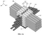
- FIGs. 1A to 1C are partial structural diagrams of a semiconductor device provided by the embodiments of the disclosure.
- the semiconductor device 10 provided by the embodiments of the disclosure includes a substrate 101, a dielectric structure 102, bit lines 103, transistors 104 (not shown in FIG. 1A ), capacitors 105 and word lines 106.
- the dielectric structure 102 includes multiple dielectric layers 1021 parallel to the substrate 101 and multiple isolation layers 1022 perpendicular to the substrate 101.
- a projection of the dielectric structure 102 in a third direction is grid-shaped.
- Bit lines 103 are perpendicular to the substrate 101 and located in the dielectric structure 102.
- Transistors 104 are parallel to the substrate 101, are connected to bit lines 103, are located in vacancies of the dielectric structure 102, and extend in the third direction as shown in FIG. 1B .
- Capacitors 105 are parallel to the substrate 101, are connected to the transistors 104, are located in the dielectric structure 102, and extend in the third direction.
- Word lines 106 are parallel to the substrate 101, are located in each dielectric layer 1021, and extend in a second direction. The second direction is perpendicular to the third direction.
- Z direction is the first direction
- Y direction is the second direction
- X direction is the third direction, as shown in FIG. 1A .
- a semiconductor device 10 provided by the embodiments of the disclosure also includes connection lines 107 for connecting the peripheral circuit and the word lines 106, to enable power supply to the word lines 106, as shown in FIG. 1C .
- a bit line is formed between two adjacent ones of the isolation layers, a transistor and a capacitor are formed based on the bit line, the capacitor is parallel to a surface of the substrate, and a word line is formed between two adjacent ones of the transistors, thereby forming a three-dimensional stacked semiconductor device.
- two transistors share a bit line by configuring the bit lines perpendicular to the substrate, and the capacitors are configured to be parallel to the substrate and located on both sides of the bit lines.
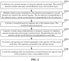
- FIG. 2 is a flow diagram of the method for forming the semiconductor device provided by the embodiments of the disclosure.
- the semiconductor device can be formed by the following operations: S201, a substrate and a stacked structure covering the substrate is provided.
- the stacked structure includes alternately stacked dielectric layers and sacrificial layers.
- multiple isolation layers extending along a first direction and arranged along a second direction are formed in the stacked structure.
- the first direction is perpendicular to a surface of the substrate.
- the second direction is perpendicular to the first direction.
- bit line is formed between two adjacent ones of the isolation layers.
- the sacrificial layers are removed.
- capacitor via holes are formed along a third direction at vacancies of the dielectric structure formed after removing the sacrificial layers.
- the third direction, the first direction and the second direction are perpendicular to each other.
- transistors and capacitors are sequentially formed in the capacitor via holes.
- the capacitors are parallel to the surface of the substrate.
- a word line extending in the second direction is formed between two adjacent ones of the transistors to form the semiconductor device.
- FIGs. 3A to 3L are partial structural diagrams corresponding to the method for forming the semiconductor device provided by the embodiments of the disclosure.
- S201 is performed to provide a substrate 301 and a stacked structure 302 covering the substrate 301.
- the stacked structure 302 includes alternately stacked dielectric layers 3021 and sacrificial layers 3022.
- the substrate 301 may be a silicon substrate, a silicon nitride substrate or a gallium nitride substrate.
- the dielectric layers 3021 may be of nitride such as silicon nitride, silicon carbonitride or silicon boron nitride, and the sacrificial layer 3022 may be of oxide such as silicon oxide.
- an oxide layer 3023 may also be formed on a surface of the stacked structure 302.
- the oxide layer 3023 represents the end of the stacked structure 302, and the oxide layer 3023 may be of silicon oxynitride.
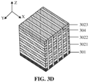
- isolation layers may be formed by the following operations: S2021, the stacked structure is etched along the first direction to form multiple isolation trenches arranged at equal intervals along the second direction.
- an isolation material is filled in the isolation trenches to form multiple isolation layers arranged at equal intervals along the second direction.
- multiple isolation trenches 303 arranged at equal intervals along the second direction may be formed in the stacked structure 302 by wet etching or dry etching, and then multiple isolation layers 304 arranged at equal intervals along the second direction may be formed by filling the isolation trenches 303 with the isolation material by physical vapor deposition (PVD), chemical vapor deposition (CVD) or atomic layer deposition (ALD).
- PVD physical vapor deposition
- CVD chemical vapor deposition
- ALD atomic layer deposition
- a material of the isolation layers 304 may be an oxide or a nitride.
- the material of the isolation layers 304 and the material of the dielectric layers 3021 may be the same or different.
- S203 is performed. A bit line between two adjacent ones of the isolation layers is formed. The sacrificial layers 3022 are removed.
- the operation that a bit line is formed may be accomplished by the following operations: S2031, a bit line via hole is formed between two adjacent ones of the isolation layers.
- the diameter of the bit line via hole is greater than or equal to the spacing between two adjacent ones of the isolation layers.
- bit line is formed in each bit via hole.
- a top surface of the bit lines is flush with a top surface of the stacked structure in the first direction.
- the stacked structure may be etched along the first direction (that is, the Z direction) between two adjacent ones of the isolation layers 304 by wet etching or dry etching until the substrate 301 is exposed, to form a bit line via 305 correspondingly , as shown in FIG. 3E .
- diameter A of the bit line via holes 305 is greater than or equal to spacing B between two adjacent ones of the isolation layers 304.
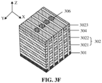
- bit lines 306 are formed in bit line via holes 305 by physical vapor deposition, chemical vapor deposition, atomic layer deposition, or epitaxial growth until the top surface of the bit lines 306 is flush with the top surface of the stacked structure, as shown in FIG. 3F .
- bit lines 306 are formed in bit line via holes 305 by the epitaxial growth
- the epitaxial growth can be performed on the basis of the silicon substrate 301, and in-situ doping can be performed during the epitaxial growth process to obtain the bit lines 306.
- a material of the bit lines 306 include tungsten (W), cobalt (Co), copper (Cu), aluminum (Al), polysilicon, doped silicon, silicide, or any combinations thereof.
- the sacrificial layers 3022 in the stack structure 302 may be removed by wet etching after forming the bit lines 306 or after removing the sacrificial layers 3022.
- the stack structure and the isolation layers 304 form a dielectric structure 307 whose projection in the third direction (that is, the X direction) is grid-shaped Vacancies of the dielectric structure 307 constitute the growth regions for the transistors and capacitors.
- Capacitor via holes are formed in the vacancies of the dielectric structure 307 along the third direction.
- the vacancies are formed after the sacrificial layers 3022 are removed. Sidewalls of the vacancies are composed of dielectric layers 3021 and isolation layers 304.
- Transistors 308 and capacitors 309 are sequentially formed in capacitor via holes may be performed by the following operations: S2051, in the third direction, based on the bit lines, the transistors are formed in the capacitor via holes by an epitaxial growth process. Sources of the transistors are connected with the bit lines.
- the transistors 308 are formed in the capacitor via holes based on the bit lines 306, the stacked structure is omitted and only the bit lines 306 and the transistors 308 are shown in FIG. 3H .
- the transistors 308 connected to the bit lines may be formed in the capacitor via holes by physical vapor deposition, chemical vapor deposition, atomic layer deposition or epitaxial growth. Where transistor 308 is formed by epitaxial growth, in-situ doping may be performed during epitaxial growth to form transistors 308.
- sources or drains of the transistors 308 contact the bit lines 306, which are not shown in the embodiments of the disclosure and the drawings.
- transistors are formed on both sides of a bit line.
- a semiconductor device structure in which multiple transistors share a bit line reduces the size of the semiconductor device and improves the performance of the semiconductor device.
- a first electrode layer is formed on inner walls of capacitor via holes and surfaces of transistors in the third direction.
- a dielectric layer covering the first electrode layer and a second electrode layer covering the dielectric layer are sequentially formed, to form a capacitor.
- the first electrode layer (not shown in the figure) is formed on surfaces of the transistors 308 at the capacitor via holes.
- the dielectric layer (not shown in the figure) covering the first electrode layer and the second electrode layer (not shown in the figure) covering the dielectric layer are formed to form the capacitors 309.
- the first electrode layer of capacitors is connected to drains of the transistors 308.
- the first electrode layer of capacitors is connected to the sources of the transistor 308.
- a material of the first electrode layer includes a metal nitride or a metal silicide.
- a material of the second electrode layer includes metal nitride or metal silicide.
- a material of the dielectric layer includes at least one of zirconium oxide, hafnium oxide, titanium zirconium oxide, ruthenium oxide, antimony oxide or aluminium oxide.
- the capacitors parallel to the substrate and located on both sides of the bit lines are formed, so that the capacitors can be infinitely superimposed in the direction perpendicular to the substrate, thereby improving the storage performance of semiconductor devices.
- a word line extending in the second direction is formed between two adjacent ones of the transistors 308.
- the word lines are connected to the gates of the transistors 308.
- the word lines may be formed by the following operations:
- a word line via hole extending in the second direction is formed in each dielectric layer at a position between two adjacent ones of the transistors.
- the figures given in the embodiments of the disclosure are all partial schematic diagrams of semiconductor devices.
- the dielectric structure still exists or there is an isolation layer outside the dielectric structure 302. These structures are not shown in the figures provided in the embodiments of the disclosure.
- word line via holes 310 extending in the second direction (that is, the Y direction) are formed on both sides of the bit lines 306 by dry etching or wet etching at positions between two adjacent ones of the transistors 308 (not shown in the figure) in each dielectric layer 3021 of the dielectric structure.
- the word line via holes 310 expose the gates of the transistors 308 (not shown in the figure).
- a gate oxide layer (not shown in the figure) is formed on the gate surface by physical vapor deposition, chemical vapor deposition, atomic layer deposition, or epitaxial growth at positions where the gates are exposed in the word line via holes 310.
- the gate oxide layer may be of a material such as silicon dioxide.
- each of the word line via holes with a gate oxide layer is filled, to form a first initial word line.
- the first initial word line may be formed in each word line via hole having the gate oxide layer by physical vapor deposition, chemical vapor deposition, atomic layer deposition or epitaxial growth.
- a dielectric layer (not shown in the figure) of the first thickness C between a first initial word line and one of the adjacent bit lines 306.
- the dielectric structure is omitted in FIG. 3K , so that the dielectric layers between the first initial word lines and the bit lines 306 are not shown in the figure.
- each first initial word line is etched back to form a word line combination. Both ends of the word line combination are step-shaped in the first direction.
- the word line combination includes at least two word lines.
- the first initial word lines are not shown in FIG. 3K . At positions not shown in the drawings of the embodiments of the disclosure, the first initial word lines extend in the second direction to a position where the bit lines 306 are not formed.
- the first initial word line is etched back at least once, so as to form a word line combination. Both ends of the word line combination are step-shaped in the first direction.
- the word line combination includes at least two word lines 311, as shown in FIG. 3K .
- the operation that the word lines 311 are formed may also be performed by the following operations: S2065, a word line via hole extending in the second direction is formed in each dielectric layer at a position between two adjacent ones of the transistors.
- each word line via hole having the gate oxide layer is filled with a first filling material to a partial depth.
- Multiple word line via holes with remaining depth form multiple stepped word line via holes. Ends of multiple stepped word line via hole at one end along the first direction are arranged in a stepped shape.
- each stepped word line via hole is filled to form a second initial word line combination with one end arranged in a stepped shape.
- the second initial word line combination includes at least two second initial word lines.
- each second initial word line is etched back to form a word line combination. Both ends of the word line combination are step-shaped in the first direction.
- the word line combination includes at least two word lines.
- the word line via holes may be filled to form stepped word line via holes with stepped shaped ends at one side
- a second initial word line combination is formed by filling, at this point, one side of the second initial word line combination is stepped shaped and the other side is flush with the opening of the word line via holes, then the flush side of the second initial word line combination is etched back to form a word line combination with both ends along the first direction arranged in a stepped shape to form stepped word lines.
- a material of word lines 311 includes tungsten (W), cobalt (Co), copper (Cu), aluminum (Al), polysilicon, doped silicon, silicide, or any combinations thereof.
- a second filling material is filled in remaining holes left after etching back. An upper surface of the second filling material is flush with the outer surface of the dielectric structure.
- the remaining holes left after etching back is word line via holes exposed again after the word lines are etched back.
- the remaining holes are filled with the second filling material until the upper surface of the second filling material is flush with the outer surface of the dielectric structure.
- the embodiments of the disclosure may also include the following operations: S20, the dielectric structure is etched along the first direction at positions corresponding to both ends of each word line, to form at least one connecting via hole. Each word line is exposed by the connecting via hole.
- each connecting via hole is filled to form a connecting line
- Each word line is connected with a connecting line.
- connecting via holes are formed at positions of the dielectric structure corresponding to both ends of each word line, and the connecting via holes expose the surfaces of the word lines. Because the ends of the word lines at both sides are in stepped shape, the connecting via holes are arranged orderly in the dielectric structure.
- connection via holes are filled to form connection lines 312.
- Each word line 311 is connected to a connection line 312, as shown in FIG. 3L Part of the dielectric structure is omitted in FIG. 3 in order to clearly show the positional relationship between the connection lines 312 and the word lines 311.
- connection between the word lines 311 and the peripheral circuit can be realized through the connection line 312, thereby powering the word lines 311.
- multiple isolation layers which extend along the first direction and are arranged along the second direction, are formed in a stacked structure formed by alternately stacked dielectric layers and sacrificial layers, one bit line is formed between each adjacent two isolation layers, transistors and capacitors are formed based on the bit lines, the capacitors are parallel to the substrate surface, and a word line is formed between each adjacent two transistors.
- a three-dimensional stacked semiconductor device is thus formed.
- two transistors share a bit line by configuring the bit lines perpendicular to the substrate, capacitors are configured to be parallel to the substrate and located on both sides of the bit line.
- the disclosed devices and methods may be implemented in a non-targeted manner.
- the above-described embodiments about devices are only illustrative, for example, the division of the units is only a logical functional division, which can be implemented in other ways, such as: multiple units or components can be combined, or can be integrated into another system, or some features can be ignored or not performed.
- the components shown or discussed are coupled with each other, or directly coupled.
- the units described above as separate elements may or may not be physically separated, and the elements displayed as elements may or may not be physical elements, that is, may be located in one place or may be distributed over multiple network elements; part or all of the units can be selected according to actual needs to achieve the purpose of the solutions of the embodiments.
- two transistors share one bit line by configuring the bit line perpendicular to the substrate, capacitors are configured to be parallel to the substrate and located on both sides of the bit line.
Landscapes
- Engineering & Computer Science (AREA)
- Manufacturing & Machinery (AREA)
- Semiconductor Memories (AREA)
Abstract
Description
- The disclosure claims priority to
Chinese Patent Application No. 202210013802.0, filed on January 7, 2022 - The embodiments of the disclosure relate to the technical field of semiconductor, and relate to but are not limited to a method for forming a semiconductor device and a semiconductor device.
- With the development of semiconductor industry, the critical dimensions of Dynamic Random Access Memory (DRAM) devices are decreasing.
- However, with the limitation of etching resolution in semiconductor manufacturing process, when semiconductor devices are formed by related technologies, the critical dimensions of semiconductor devices cannot be infinitely reduced. Therefore, how to realize stacking of semiconductor device is an urgent problem to be solved in the semiconductor field.
- In view of this, embodiments of the disclosure provide a method for forming a semiconductor device and a semiconductor device.
- In a first aspect, the embodiments of the disclosure provide a method for forming a semiconductor device. The method includes following operations.
- A substrate and a stacked structure covering the substrate are provided. The stacked structure includes alternately stacked dielectric layers and sacrificial layers.
- Multiple isolation layers extending in a first direction and arranged in a second direction are formed in the stacked structure. The first direction is perpendicular to the substrate surface. The second direction is perpendicular to the first direction
- A bit line is formed between two adjacent ones of the isolation layers. The sacrificial layers are removed.
- Capacitor via holes along a third direction is formed in vacancies of a dielectric structure. The dielectric structure is formed after removing the sacrificial layers. The third direction, the first direction and the second direction are perpendicular to each other.
- Transistors and capacitors are formed sequentially in capacitor via holes based on bit lines. The capacitors are parallel to the substrate surface.
- A word line extending in the second direction is formed between two adjacent ones of the transistors to form the semiconductor device.
- In some embodiments, the operation that multiple isolation layers extending in a first direction and arranged in a second direction are formed in the stacked structure includes following operations.
- The stacked structure is etched along the first direction to form multiple isolation trenches arranged at an equal interval along the second direction.
- The isolation trenches are filled with an isolation material, to form the multiple isolation layers arranged at an equal interval along the second direction.
- In some embodiments, the dielectric structure is formed after removing the sacrificial layers.
- A projection of the dielectric structure in the third direction is grid-shaped. The vacancies in the dielectric structure constitute growth regions for the transistors and the capacitors.
- In some embodiments, the operation that a bit line is formed between two adjacent ones of the isolation layers includes the following operations.
- A bit via hole is formed between two adjacent ones of the isolation layers. The diameter of the bit via hole is greater than or equal to the interval between two adjacent ones of the isolation layers.
- A bit line is formed in bit line via hole. In the first direction, the top surface of the bit line is flush with the top surface of the stacked structure.
- In some embodiments, the operation that a bit line via is formed between two adjacent ones of the isolation layers includes following operation.
- The stacked structure is etched in the first direction between two adjacent ones of the isolation layers until the substrate is exposed, to correspondingly form the bit line via hole.
- In some embodiments, the operation that transistors and capacitors are sequentially formed in the capacitor via holes based on the bit lines includes the following operations.
- The transistors are formed in the capacitor via holes in the third direction by an epitaxial growth process based on the bit lines. The sources of the transistors are connected with the bit lines.
- First electrode layers are formed on inner walls of the capacitor via holes and surfaces of the transistors in the third direction.
- Dielectric layers covering the first electrode layers and second electrode layers covering the dielectric layers are sequentially formed to form the capacitors.
- In some embodiments, the operation that a word line extending in the second direction is formed between two adjacent ones of the transistors includes the following operations.
- A word line via hole extending in the second direction is formed in each of the dielectric layers at a position between two adjacent ones of the transistors.
- A gate oxide layer covering a lower surface of each of word line via holes is formed in the first direction.
- Each of the word line via holes having the gate oxide layer is filled to form first initial word lines. There is a dielectric layer with a first thickness between each word line and one of its adjacent bit lines in the third direction.
- Each of the first initial word lines is etched back to form a word line combination. The word line combination is arranged in a stepped shape at both ends along the first direction. The word line combination includes at least two word lines.
- In some embodiments, the operation that each of the first initial word lines is etched back includes the following operation.
- At both ends of each of the first initial word lines, the first initial word lines are etched back at least once.
- In some embodiments, the operation that a word line extending in the second direction is formed between two adjacent ones of the transistors includes the following operations.
- A word line via hole extending in the second direction is formed in each of the dielectric layers at a position between two adjacent ones of the transistors.
- Each of the word line via holes is filled with a first filling material with a partial depth. Multiple word line via holes with a remaining depth form multiple stepped word line via holes. The multiple stepped word line via holes at one end along the first direction are arranged in a stepped shape.
- Each stepped word line via hole is filled to form a second initial word line combination with one end arranged in the stepped shape. The second initial word line combination includes at least two second initial word lines.
- Each of the second initial word lines is etched back to form a word line combination with both ends along the first direction arranged in the stepped shape. The word line combination includes at least two word lines.
- In some embodiments, after forming word lines, the method further includes the following operation.
- A second filling material is filled in the remaining holes left after etching back. The upper surface of the second filling material and the outer surface of the dielectric structure are flush.
- In some embodiments, after forming word lines, the method further includes the following operations.
- The dielectric structure is etched along the first direction at positions corresponding to both ends of each word line to form at least one connecting via hole. The connecting via hole exposes a corresponding word lines.
- The connecting via holes are filled to form connecting lines. Each word line is connected with two connecting lines.
- In some embodiments, after providing the stacked structure, the method further includes the following operation.
- An oxide layer covering the stacked structure is formed. The oxide layer is connected to an uppermost sacrificial layer in the stacked structure;
Correspondingly, the operation that multiple isolation layers extending in the first direction and arranged in the second direction are formed in the stacked structure includes the following operation. - The multiple isolation layers extending in the first direction and arranged at equal interval in the second direction are formed in the stacked structure and the oxide layer.
- In a second aspect, the embodiments of the disclosure provide a semiconductor device. The semiconductor device includes a substrate, a dielectric structure, bit lines, transistors, capacitors and word lines.
- The dielectric structure includes multiple dielectric layers parallel to the substrate and multiple isolation layers perpendicular to the substrate. A projection of the dielectric structure in a third direction is grid-shaped.
- The bit lines are perpendicular to the substrate and located in the dielectric structure.
- The transistors are parallel to the substrate, connected to the bit lines, located in vacancies of the dielectric structure and extending in the third direction.
- The capacitors are parallel to the substrate, connected to the transistors, located in the dielectric structure and extending in the third direction; and
The word lines are parallel to the substrate, located in each of the dielectric layers and extending in a second direction. The second direction is perpendicular to the third direction. - In some embodiments, the capacitors include at least first electrode layers, dielectric layers and second electrode layers.
- The first electrode layers are in contact with the transistors and located in the dielectric structure.
- The dielectric layers cover surfaces of the first electrode layers.
- The second electrode layers cover surfaces of the dielectric layers.
- In some embodiments, both ends of a word line combination are step-shaped. The word line combination is formed by at least one word line.
- In some embodiments, in the dielectric structure, a bit line is connected to a transistor at both sides along the third direction.
- In some embodiments, the semiconductor device further includes connecting lines for connecting a peripheral circuit and the word lines to power the word lines.
- A method for forming a semiconductor device and a semiconductor device are provided according to the embodiments of the disclosure. Multiple isolation layers extending along the first direction and arranged along the second direction are formed in a stacked structure. The stacked structure is formed by alternately stacking dielectric layers and sacrificial layers. A bit line is formed between two adjacent ones of the isolation layers. Transistors and capacitors are formed based on the bit lines. The capacitors are parallel to the substrate surface. A word line is formed between two adjacent ones of the transistors to form a three-dimensional stacked semiconductor device. In this way, in the embodiments of the disclosure, two transistors share a bit line by configuring the bit lines perpendicular to the substrate, and the capacitors are configured to be parallel to the substrate and located on both sides of the bit line. By doing so, the embodiments of the disclosure can reduce the size of key devices and improve the performance of semiconductor devices by sharing a bit line while realizing three-dimensional stacking.
- In the drawings (which are not necessarily drawn to scale), similar reference numbers may describe similar components in different views. Similar reference numbers with different letter suffixes may denote different examples of similar components. The drawings generally illustrate various embodiments discussed herein by way of example and not limitation.
-
FIGs. 1A to 1C are partial structural diagrams of a semiconductor device provided by the embodiments of the disclosure. -
FIG. 2 is a flow diagram of a method for forming a semiconductor device provided by the embodiments of the disclosure. -
FIGs. 3A to 3L are partial structural diagrams corresponding to the method for forming the semiconductor device provided by the embodiments of the disclosure. - 101-substrate; 102-dielectric structure; 1021-dielectric layer; 1022-isolation layer; 103-bit line; 104-transistor; 105-capacitor; 106-word line;107-connecting line;301-substrate; 302-stacked structure; 3021-dielectric layer; 3022-sacrificial layer; 3023-oxide layer; 303-isolation trench; 304-isolation layer; 305-bit line via hole; 306-bit line; 307-dielectric structure; 308-transistor; 309-capacitor; 310-word line via hole; 311-word line; 312-connecting line.
- In order to make the purpose, technical solutions and advantages of the embodiments of the disclosure clearer, the specific technical solutions of the disclosure will be described in further detail below in conjunction with the accompanying drawings in the embodiments of the disclosure. The following embodiments are used to illustrate the disclosure, but are not intended to limit the scope of the disclosure.
- In the following description, numerous specific details are given to provide a more thorough understanding of the disclosure. However it will be apparent to a person skilled in the art that the disclosure may be practiced without one or more of these details. In other examples, some technical features well known in the art are not described in order to avoid confusion with the disclosure; that is, all features of actual embodiments are not described herein, and well-known functions and structures are not described in detail.
- In the drawings, the dimensions of layers, regions, elements and their relative dimensions may be exaggerated for clarity. Throughout, the same reference numbers denote the same elements.
- It is to be understood that description that an element or layer is "on", "adjacent to", "connected to", or "coupled to" another element or layer may refer to that the element or layer is directly on, adjacent to, connected to or coupled to the other element or layer, or there may be an intermediate element or layer. On the contrary, description that an element is "directly on", "directly adjacent to", "directly connected to" or "directly coupled to" another element or layer refers to that there is no intermediate element or layer. It is to be understood, although various elements, components, regions, layers and/or parts may be described with terms first, second, third, etc., these elements, components, regions, layers and/or parts should not be limited by these terms. These terms are used only to distinguish one element, component, area, layer or part from another element, component, area, layer or part. Therefore, a first element, component, region, layer or part discussed below may be represented as a second element, component, region, layer or part without departing from the teaching of the disclosure. A second element, component, region, layer or part does not imply that a first element, component, region, layer or part is necessarily present in the disclosure.
- Spatially relational terms such as "below", "under", "lower", "beneath", "above", and "upper" may be used herein for conveniently describing a relationship between one element or feature and another element or feature illustrated in the figures. It is to be understood that, in addition to the orientation shown in the figures, the spatially relational terms further include different orientations of devices in use and operation. For example, if the devices in the figures are turned over, elements or features described as being "under" or "beneath" or "below" other elements or features will be oriented to be "on" the other elements or features. Therefore, the exemplary terms "under" and "below" may include both upper and lower orientations. Moreover, the device may include otherwise orientation (rotation by 90 degrees or in other orientations) and the spatial descriptors used herein may be interpreted accordingly.
- The terminology used herein is intended to describe the specific embodiments only and is not to be a limitation of the disclosure. As used herein, singular forms of "a", "an" and "said/the" are also intended to include the plural forms, unless the context clearly indicates otherwise. It should also be understood that the terms "including" and/or "comprising", when used in this specification, determine the presence of said features, integers, steps, operations, elements and/or components, but do not exclude the presence or addition of one or more other features, integers, steps, operations, elements, components and/or groups. As used herein, the term "and/or" includes any and all combinations of related listed items.
- Based on problems existing in the related art, the embodiments of the disclosure provide a semiconductor device, as shown in
FIGs. 1A and1B .FIGs. 1A to 1C are partial structural diagrams of a semiconductor device provided by the embodiments of the disclosure. Thesemiconductor device 10 provided by the embodiments of the disclosure includes asubstrate 101, adielectric structure 102,bit lines 103, transistors 104 (not shown inFIG. 1A ),capacitors 105 and word lines 106. Thedielectric structure 102 includes multipledielectric layers 1021 parallel to thesubstrate 101 andmultiple isolation layers 1022 perpendicular to thesubstrate 101. A projection of thedielectric structure 102 in a third direction is grid-shaped.Bit lines 103 are perpendicular to thesubstrate 101 and located in thedielectric structure 102.Transistors 104 are parallel to thesubstrate 101, are connected to bitlines 103, are located in vacancies of thedielectric structure 102, and extend in the third direction as shown inFIG. 1B .Capacitors 105 are parallel to thesubstrate 101, are connected to thetransistors 104, are located in thedielectric structure 102, and extend in the third direction.Word lines 106 are parallel to thesubstrate 101, are located in eachdielectric layer 1021, and extend in a second direction. The second direction is perpendicular to the third direction. - In the embodiments of the disclosure, Z direction is the first direction, Y direction is the second direction, and the X direction is the third direction, as shown in
FIG. 1A . - In some embodiments, a
semiconductor device 10 provided by the embodiments of the disclosure also includesconnection lines 107 for connecting the peripheral circuit and the word lines 106, to enable power supply to the word lines 106, as shown inFIG. 1C . - In the embodiments of the disclosure, by forming multiple isolation layers extending along the first direction and arranged along the second direction, in a stacked structure formed by alternately stacking dielectric layers and sacrificial layers, a bit line is formed between two adjacent ones of the isolation layers, a transistor and a capacitor are formed based on the bit line, the capacitor is parallel to a surface of the substrate, and a word line is formed between two adjacent ones of the transistors, thereby forming a three-dimensional stacked semiconductor device. In this way, in the embodiments of the disclosure, two transistors share a bit line by configuring the bit lines perpendicular to the substrate, and the capacitors are configured to be parallel to the substrate and located on both sides of the bit lines. By doing so, the embodiments of the disclosure can reduce the size of key devices and improve the performance of semiconductor devices by sharing a bit line while realizing three-dimensional stacking.
- Based on the semiconductor device provided by the foregoing embodiments, the embodiments of the disclosure further provide a method for forming the semiconductor device.
FIG. 2 is a flow diagram of the method for forming the semiconductor device provided by the embodiments of the disclosure. As shown inFIG. 2 , the semiconductor device can be formed by the following operations:
S201, a substrate and a stacked structure covering the substrate is provided. The stacked structure includes alternately stacked dielectric layers and sacrificial layers. - S202, multiple isolation layers extending along a first direction and arranged along a second direction are formed in the stacked structure. The first direction is perpendicular to a surface of the substrate. The second direction is perpendicular to the first direction.
- S203, a bit line is formed between two adjacent ones of the isolation layers. The sacrificial layers are removed.
- S204, capacitor via holes are formed along a third direction at vacancies of the dielectric structure formed after removing the sacrificial layers. The third direction, the first direction and the second direction are perpendicular to each other.
- S205, based on the bit lines, transistors and capacitors are sequentially formed in the capacitor via holes. The capacitors are parallel to the surface of the substrate.
- S206, a word line extending in the second direction is formed between two adjacent ones of the transistors to form the semiconductor device.
- Next, the method for forming the semiconductor device provided by the embodiments of the disclosure will be further described in detail with reference to
FIGs. 3A to 3L which are partial structural diagrams corresponding to the method for forming the semiconductor device provided by the embodiments of the disclosure. - As shown in
FIG. 3A , S201 is performed to provide asubstrate 301 and astacked structure 302 covering thesubstrate 301. Thestacked structure 302 includes alternately stackeddielectric layers 3021 andsacrificial layers 3022. - In some embodiments, the
substrate 301 may be a silicon substrate, a silicon nitride substrate or a gallium nitride substrate. Thedielectric layers 3021 may be of nitride such as silicon nitride, silicon carbonitride or silicon boron nitride, and thesacrificial layer 3022 may be of oxide such as silicon oxide. - In some embodiments, as shown in
FIG. 3B , after forming thestacked structure 302, anoxide layer 3023 may also be formed on a surface of the stackedstructure 302. Theoxide layer 3023 represents the end of the stackedstructure 302, and theoxide layer 3023 may be of silicon oxynitride. - Next, referring to
FIGs. 3C and3D , S202 is performed. In the embodiments of the disclosure, isolation layers may be formed by the following operations:
S2021, the stacked structure is etched along the first direction to form multiple isolation trenches arranged at equal intervals along the second direction. - S2022, an isolation material is filled in the isolation trenches to form multiple isolation layers arranged at equal intervals along the second direction.
- Referring to
FIGs. 3C and3D ,multiple isolation trenches 303 arranged at equal intervals along the second direction (that is, the Y direction) may be formed in thestacked structure 302 by wet etching or dry etching, and then multiple isolation layers 304 arranged at equal intervals along the second direction may be formed by filling theisolation trenches 303 with the isolation material by physical vapor deposition (PVD), chemical vapor deposition (CVD) or atomic layer deposition (ALD). - In some embodiments, a material of the isolation layers 304 may be an oxide or a nitride. The material of the isolation layers 304 and the material of the
dielectric layers 3021 may be the same or different. - Next referring to
FIGs. 3E to 3G , S203 is performed. A bit line between two adjacent ones of the isolation layers is formed. Thesacrificial layers 3022 are removed. - In some embodiments, the operation that a bit line is formed may be accomplished by the following operations:
S2031, a bit line via hole is formed between two adjacent ones of the isolation layers. The diameter of the bit line via hole is greater than or equal to the spacing between two adjacent ones of the isolation layers. - S2032, a bit line is formed in each bit via hole. A top surface of the bit lines is flush with a top surface of the stacked structure in the first direction.
- In some embodiments, the stacked structure may be etched along the first direction (that is, the Z direction) between two adjacent ones of the isolation layers 304 by wet etching or dry etching until the
substrate 301 is exposed, to form a bit line via 305 correspondingly , as shown inFIG. 3E . - In some embodiments, diameter A of the bit line via
holes 305 is greater than or equal to spacing B between two adjacent ones of the isolation layers 304. By doing so, when transistors are subsequently formed on both sides of each bit line along the third direction in the stacked structure, the transistors on both sides are not connected to each other, thereby avoiding a transistor failure. - In some embodiments, after forming the bit line via
holes 305,bit lines 306 are formed in bit line viaholes 305 by physical vapor deposition, chemical vapor deposition, atomic layer deposition, or epitaxial growth until the top surface of the bit lines 306 is flush with the top surface of the stacked structure, as shown inFIG. 3F . - In the embodiments of the disclosure, where
bit lines 306 are formed in bit line viaholes 305 by the epitaxial growth, the epitaxial growth can be performed on the basis of thesilicon substrate 301, and in-situ doping can be performed during the epitaxial growth process to obtain the bit lines 306. A material of thebit lines 306 include tungsten (W), cobalt (Co), copper (Cu), aluminum (Al), polysilicon, doped silicon, silicide, or any combinations thereof. - In some embodiments, the
sacrificial layers 3022 in thestack structure 302 may be removed by wet etching after forming thebit lines 306 or after removing thesacrificial layers 3022. The stack structure and the isolation layers 304 form adielectric structure 307 whose projection in the third direction (that is, the X direction) is grid-shaped Vacancies of thedielectric structure 307 constitute the growth regions for the transistors and capacitors. - Next, S204 is performed. Capacitor via holes are formed in the vacancies of the
dielectric structure 307 along the third direction. The vacancies are formed after thesacrificial layers 3022 are removed. Sidewalls of the vacancies are composed ofdielectric layers 3021 and isolation layers 304. - Referring to
FIGs. 3H and3I , S205 is performed.Transistors 308 andcapacitors 309 are sequentially formed in capacitor via holes may be performed by the following operations:
S2051, in the third direction, based on the bit lines, the transistors are formed in the capacitor via holes by an epitaxial growth process. Sources of the transistors are connected with the bit lines. - Referring to
FIG. 3H , thetransistors 308 are formed in the capacitor via holes based on thebit lines 306, the stacked structure is omitted and only thebit lines 306 and thetransistors 308 are shown inFIG. 3H . In the embodiments of the disclosure thetransistors 308 connected to the bit lines may be formed in the capacitor via holes by physical vapor deposition, chemical vapor deposition, atomic layer deposition or epitaxial growth. Wheretransistor 308 is formed by epitaxial growth, in-situ doping may be performed during epitaxial growth to formtransistors 308. - In the embodiments of the disclosure, after the
transistors 308 are formed, sources or drains of thetransistors 308 contact thebit lines 306, which are not shown in the embodiments of the disclosure and the drawings. - As shown in
FIG. 3H , in the embodiments of the disclosure, transistors are formed on both sides of a bit line. A semiconductor device structure in which multiple transistors share a bit line reduces the size of the semiconductor device and improves the performance of the semiconductor device. - S2052, a first electrode layer is formed on inner walls of capacitor via holes and surfaces of transistors in the third direction.
- S2053, a dielectric layer covering the first electrode layer and a second electrode layer covering the dielectric layer are sequentially formed, to form a capacitor.
- Next, referring to
FIG. 3I , after forming thetransistors 308, the first electrode layer (not shown in the figure) is formed on surfaces of thetransistors 308 at the capacitor via holes. The dielectric layer (not shown in the figure) covering the first electrode layer and the second electrode layer (not shown in the figure) covering the dielectric layer are formed to form thecapacitors 309. - In the embodiments of the disclosure, where sources of the
transistors 308 are connected to thebit lines 306, the first electrode layer of capacitors is connected to drains of thetransistors 308. When drains oftransistors 308 are connected to thebit lines 306, the first electrode layer of capacitors is connected to the sources of thetransistor 308. - In the embodiments of the disclosure, a material of the first electrode layer includes a metal nitride or a metal silicide. A material of the second electrode layer includes metal nitride or metal silicide. A material of the dielectric layer includes at least one of zirconium oxide, hafnium oxide, titanium zirconium oxide, ruthenium oxide, antimony oxide or aluminium oxide.
- In the embodiments of the disclosure, based on the bit lines perpendicular to the substrate, the capacitors parallel to the substrate and located on both sides of the bit lines are formed, so that the capacitors can be infinitely superimposed in the direction perpendicular to the substrate, thereby improving the storage performance of semiconductor devices.
- Next, referring to
FIGs. 3J and3L , S206 is performed. A word line extending in the second direction is formed between two adjacent ones of thetransistors 308. In some embodiments, the word lines are connected to the gates of thetransistors 308. In the embodiments of the disclosure, the word lines may be formed by the following operations: - S2061, a word line via hole extending in the second direction is formed in each dielectric layer at a position between two adjacent ones of the transistors.
- The figures given in the embodiments of the disclosure are all partial schematic diagrams of semiconductor devices. In addition to the structures given in the figures, the dielectric structure still exists or there is an isolation layer outside the
dielectric structure 302. These structures are not shown in the figures provided in the embodiments of the disclosure. - Referring to
FIG. 3J , word line viaholes 310 extending in the second direction (that is, the Y direction) are formed on both sides of thebit lines 306 by dry etching or wet etching at positions between two adjacent ones of the transistors 308 (not shown in the figure) in eachdielectric layer 3021 of the dielectric structure. The word line viaholes 310 expose the gates of the transistors 308 (not shown in the figure). - S2062, in the first direction, a gate oxide layer covering a bottom surface of each word line via hole is formed.
- In some embodiments, before the word lines are formed, a gate oxide layer (not shown in the figure) is formed on the gate surface by physical vapor deposition, chemical vapor deposition, atomic layer deposition, or epitaxial growth at positions where the gates are exposed in the word line via
holes 310. The gate oxide layer may be of a material such as silicon dioxide. - S2063, each of the word line via holes with a gate oxide layer is filled, to form a first initial word line. There is a dielectric layer having a first thickness between an initial word line and one of the adjacent bit lines in the third direction.
- In the embodiments of the disclosure, the first initial word line may be formed in each word line via hole having the gate oxide layer by physical vapor deposition, chemical vapor deposition, atomic layer deposition or epitaxial growth. There is a dielectric layer (not shown in the figure) of the first thickness C between a first initial word line and one of the adjacent bit lines 306. In order to show the positional relationship between the first initial word lines and the transistors, the dielectric structure is omitted in
FIG. 3K , so that the dielectric layers between the first initial word lines and thebit lines 306 are not shown in the figure. - S2064, each first initial word line is etched back to form a word line combination. Both ends of the word line combination are step-shaped in the first direction. The word line combination includes at least two word lines.
- In the embodiments of the disclosure, the first initial word lines are not shown in
FIG. 3K . At positions not shown in the drawings of the embodiments of the disclosure, the first initial word lines extend in the second direction to a position where thebit lines 306 are not formed. - In some embodiments, in order to realize a connection between each word line and a peripheral circuit, it is necessary to form a connection line to connect the word line and the peripheral circuit. Therefore, in the embodiments of the disclosure, at both ends of each first initial word line, the first initial word line is etched back at least once, so as to form a word line combination. Both ends of the word line combination are step-shaped in the first direction. The word line combination includes at least two
word lines 311, as shown inFIG. 3K . - In some embodiments, the operation that the word lines 311 are formed may also be performed by the following operations:
S2065, a word line via hole extending in the second direction is formed in each dielectric layer at a position between two adjacent ones of the transistors. - S2066, in the first direction, a gate oxide layer covering a lower surface of each word line via hole is formed.
- S2067, each word line via hole having the gate oxide layer is filled with a first filling material to a partial depth. Multiple word line via holes with remaining depth form multiple stepped word line via holes. Ends of multiple stepped word line via hole at one end along the first direction are arranged in a stepped shape.
- S2068, each stepped word line via hole is filled to form a second initial word line combination with one end arranged in a stepped shape. The second initial word line combination includes at least two second initial word lines.
- S2069, each second initial word line is etched back to form a word line combination. Both ends of the word line combination are step-shaped in the first direction. The word line combination includes at least two word lines.
- In the embodiment of the disclosure, after forming word line via holes extending along the second direction, the word line via holes may be filled to form stepped word line via holes with stepped shaped ends at one side, a second initial word line combination is formed by filling, at this point, one side of the second initial word line combination is stepped shaped and the other side is flush with the opening of the word line via holes, then the flush side of the second initial word line combination is etched back to form a word line combination with both ends along the first direction arranged in a stepped shape to form stepped word lines.
- In some embodiments, a material of
word lines 311 includes tungsten (W), cobalt (Co), copper (Cu), aluminum (Al), polysilicon, doped silicon, silicide, or any combinations thereof. - In some embodiments, after forming the word lines 311, the following operations may also be included:
S10, a second filling material is filled in remaining holes left after etching back. An upper surface of the second filling material is flush with the outer surface of the dielectric structure. - In some embodiments, the remaining holes left after etching back is word line via holes exposed again after the word lines are etched back. The remaining holes are filled with the second filling material until the upper surface of the second filling material is flush with the outer surface of the dielectric structure.
- In some embodiments, after forming the word lines 311, in order to connect word lines and a peripheral circuit, it is necessary to form a connection line to connect the word lines and the peripheral circuit. Therefore, the embodiments of the disclosure may also include the following operations:
S20, the dielectric structure is etched along the first direction at positions corresponding to both ends of each word line, to form at least one connecting via hole. Each word line is exposed by the connecting via hole. - S30, each connecting via hole is filled to form a connecting line Each word line is connected with a connecting line.
- In the embodiments of the disclosure, connecting via holes are formed at positions of the dielectric structure corresponding to both ends of each word line, and the connecting via holes expose the surfaces of the word lines. Because the ends of the word lines at both sides are in stepped shape, the connecting via holes are arranged orderly in the dielectric structure.
- In some embodiments, after forming the connection via holes, connection via holes are filled to form connection lines 312. Each
word line 311 is connected to aconnection line 312, as shown inFIG. 3L Part of the dielectric structure is omitted inFIG. 3 in order to clearly show the positional relationship between theconnection lines 312 and the word lines 311. - In some embodiments, after the
connection lines 312 are formed, the connection between the word lines 311 and the peripheral circuit can be realized through theconnection line 312, thereby powering the word lines 311. - In the embodiments of the disclosure, multiple isolation layers, which extend along the first direction and are arranged along the second direction, are formed in a stacked structure formed by alternately stacked dielectric layers and sacrificial layers, one bit line is formed between each adjacent two isolation layers, transistors and capacitors are formed based on the bit lines, the capacitors are parallel to the substrate surface, and a word line is formed between each adjacent two transistors. A three-dimensional stacked semiconductor device is thus formed. In this way, in the embodiments of the disclosure, two transistors share a bit line by configuring the bit lines perpendicular to the substrate, capacitors are configured to be parallel to the substrate and located on both sides of the bit line. By doing so, the embodiments of the disclosure can reduce the size of key devices and improve the performance of semiconductor devices by sharing the bit line while realizing three-dimensional stacking.
- In several embodiments provided by the disclosure, it should be understood that the disclosed devices and methods may be implemented in a non-targeted manner. The above-described embodiments about devices are only illustrative, for example, the division of the units is only a logical functional division, which can be implemented in other ways, such as: multiple units or components can be combined, or can be integrated into another system, or some features can be ignored or not performed. In addition, the components shown or discussed are coupled with each other, or directly coupled.
- The units described above as separate elements may or may not be physically separated, and the elements displayed as elements may or may not be physical elements, that is, may be located in one place or may be distributed over multiple network elements; part or all of the units can be selected according to actual needs to achieve the purpose of the solutions of the embodiments.
- Features disclosed in several method or device embodiments provided in the disclosure can be arbitrarily combined without conflict to obtain new method or device embodiments.
- The above-mentioned is only the specific embodiments of the disclosure, but the scope of protection of the disclosure is not limited thereto. Any skilled person familiar with the technical field can easily think of changes or substitutions within the technical scope of the disclosure, and should be covered within the scope of protection of the disclosure. Therefore, the scope of protection of this disclosure shall be subject to the scope of protection of the claims.
- In the embodiments of the disclosure, two transistors share one bit line by configuring the bit line perpendicular to the substrate, capacitors are configured to be parallel to the substrate and located on both sides of the bit line. By doing so, the embodiments of the disclosure can reduce the size of key devices and improve the performance of semiconductor devices by sharing the bit line while realizing three-dimensional stacking.
Claims (17)
- A method for forming a semiconductor device, comprising:providing a substrate and a stacked structure covering the substrate, wherein the stacked structure comprises alternately stacked dielectric layers and sacrificial layers;forming a plurality of isolation layers extending in a first direction and arranged in a second direction in the stacked structure, wherein the first direction is perpendicular to a surface of the substrate, and the second direction is perpendicular to the first direction;forming a bit line between two adjacent ones of the isolation layers and removing the sacrificial layers;forming capacitor via holes along a third direction at vacancies of a dielectric structure, of which the dielectric structure being formed after removing the sacrificial layers, wherein the third direction, the first direction and the second direction are perpendicular to each other;forming transistors and capacitors sequentially in the capacitor via holes based on bit lines, the capacitors being parallel to the surface of the substrate; andforming a word line extending in the second direction between two adjacent ones of the transistors to form the semiconductor device.
- The method according to claim 1, wherein the forming a plurality of isolation layers extending in a first direction and arranged in a second direction in the stacked structure comprises:etching the stacked structure along the first direction to form a plurality of isolation trenches arranged at an equal interval along the second direction; andfilling the isolation trenches with an isolation material to form the plurality of isolation layers arranged at an equal interval along the second direction.
- The method according to claim 1, wherein the dielectric structure is formed after removing the sacrificial layers;
wherein a projection of the dielectric structure in the third direction is grid-shaped, and the vacancies of the dielectric structure constitute growth regions for the transistors and the capacitors. - The method according to claim 1, wherein the forming a bit line between two adjacent ones of the isolation layers comprises:forming a bit line via hole between the two adjacent ones of the isolation layers, wherein a diameter of the bit line via hole is greater than or equal to an interval between two adjacent ones of the isolation layers; andforming the bit line in the bit line via hole, wherein a top surface of the bit line is flush with a top surface of the stacked structure in the first direction.
- The method according to claim 4, wherein the forming a bit line via hole between the two adjacent ones of the isolation layers comprises:
etching the stacked structure along the first direction between the two adjacent ones of the isolation layers until the substrate is exposed, to correspondingly form the bit line via hole. - The method according to claim 1, wherein the forming transistors and capacitors sequentially in the capacitor via holes based on bit lines comprises:forming the transistors in the capacitor via holes in the third direction by an epitaxial growth process based on the bit lines, sources of the transistors being connected with the bit lines;forming first electrode layers on inner walls of the capacitor via holes and surfaces of the transistors in the third direction; andforming dielectric layers covering the first electrode layers and second electrode layers covering the dielectric layers sequentially to form the capacitors.
- The method according to claim 1, wherein the forming a word line extending in the second direction between two adjacent ones of the transistors comprises:forming a word line via hole extending in the second direction in each of the dielectric layers at a position between two adjacent ones of the transistors;forming a gate oxide layer covering a lower surface of each of word line via holes in the first direction;filling each of the word line via holes having the gate oxide layer to form first initial word lines, wherein a dielectric layer having a first thickness is located between a first initial word line and the bit line in the third direction; andetching back each of the first initial word lines to form a word line combination, the word line combination being arranged in a stepped shape at both ends along the first direction, wherein the word line combination comprises at least two word lines.
- The method according to claim 7, wherein the etching back each of the first initial word lines comprises:
etching back the first initial word lines at least once at both ends of each of the first initial word lines. - The method according to claim 1, wherein the forming a word line extending in the second direction between two adjacent ones of the transistors comprises:forming a word line via hole extending in the second direction in each of the dielectric layers at a position between two adjacent ones of the transistors;forming a gate oxide layer covering a lower surface of each of word line via holes in the first direction;filling each of the word line via holes having the gate oxide layer with a first filling material to a partial depth, wherein a plurality of word line via holes with a remaining depth form a plurality of stepped word line via holes, and the plurality of stepped word line via holes at one end along the first direction are arranged in a stepped shape;filling each of the stepped word line via holes to form a second initial word line combination with one end arranged in the stepped shape, wherein the second initial word line combination comprises at least two second initial word lines; andetching back each of second initial word lines to form a word line combination with both ends along the first direction arranged in the stepped shape, wherein the word line combination comprises the at least two word lines.
- The method according to claim 7 or 9, wherein after the forming a word line, the method further comprises:
filling a second filling material in remaining holes left after etching back, wherein an upper surface of the second filling material and an outer surface of the dielectric structure are flush. - The method according to claim 1, wherein after the forming a word line, the method further comprises:etching the dielectric structure along the first direction at positions corresponding to both ends of each of word lines to form at least one connecting via hole, the connecting via hole exposing a corresponding word line; andfilling connecting via holes to form connecting lines, and each of the word lines being connected with two connecting lines.
- The method according to claim 1, wherein after providing the stacked structure, the method further comprises:forming an oxide layer covering the stacked structure, the oxide layer being connected to an uppermost sacrificial layer in the stacked structure;correspondingly, wherein the forming a plurality of isolation layers extending in a first direction and arranged in a second direction in the stacked structure comprises:
forming the plurality of isolation layers extending in the first direction and arranged at the equal interval in the second direction in the stacked structure and the oxide layer. - A semiconductor device, comprising:a substrate;a dielectric structure, comprising a plurality of dielectric layers parallel to the substrate and a plurality of isolation layers perpendicular to the substrate, a projection of the dielectric structure in a third direction being grid-shaped;bit lines perpendicular to the substrate, located in the dielectric structure;transistors parallel to the substrate, connected to the bit lines, located in vacancies of the dielectric structure and extending in the third direction;capacitors parallel to the substrate, connected to the transistors, located in the dielectric structure and extending in the third direction; andword lines parallel to the substrate, located in each of the dielectric layers and extending in a second direction, wherein the second direction is perpendicular to the third direction.
- The semiconductor device according to claim 13, wherein the capacitors comprise at least:first electrode layers in contact with the transistors and located in the dielectric structure;dielectric layers covering surfaces of the first electrode layers; andsecond electrode layers covering surfaces of the dielectric layers.
- The semiconductor device according to claim 13, wherein both ends of a word line combination are step-shaped, and the word line combination is formed by at least one word line.
- The semiconductor device according to claim 13, wherein in the dielectric structure, a bit line is connected to a transistor at both sides along the third direction.
- The semiconductor device according to claim 13, wherein the semiconductor device further comprises:
connecting lines, used for connecting a peripheral circuit and the word lines to power the word lines.
Applications Claiming Priority (2)
| Application Number | Priority Date | Filing Date | Title |
|---|---|---|---|
| CN202210013802.0A CN114023703B (en) | 2022-01-07 | 2022-01-07 | Semiconductor device forming method and semiconductor device |
| PCT/CN2022/081165 WO2023130576A1 (en) | 2022-01-07 | 2022-03-16 | Semiconductor device forming method and semiconductor device |
Publications (2)
| Publication Number | Publication Date |
|---|---|
| EP4325576A1 true EP4325576A1 (en) | 2024-02-21 |
| EP4325576A4 EP4325576A4 (en) | 2024-09-18 |
Family
ID=80069741
Family Applications (1)
| Application Number | Title | Priority Date | Filing Date |
|---|---|---|---|
| EP22918042.7A Pending EP4325576A4 (en) | 2022-01-07 | 2022-03-16 | METHOD FOR FORMING SEMICONDUCTOR DEVICE AND SEMICONDUCTOR DEVICE |
Country Status (4)
| Country | Link |
|---|---|
| US (1) | US12513885B2 (en) |
| EP (1) | EP4325576A4 (en) |
| CN (1) | CN114023703B (en) |
| WO (1) | WO2023130576A1 (en) |
Families Citing this family (27)
| Publication number | Priority date | Publication date | Assignee | Title |
|---|---|---|---|---|
| CN114023703B (en) | 2022-01-07 | 2022-04-26 | 长鑫存储技术有限公司 | Semiconductor device forming method and semiconductor device |
| KR102752338B1 (en) | 2022-03-23 | 2025-01-10 | 창신 메모리 테크놀로지즈 아이엔씨 | Memory and its manufacturing method |
| CN116867262A (en) * | 2022-03-23 | 2023-10-10 | 长鑫存储技术有限公司 | Semiconductor structure and manufacturing method, memory |
| CN114759033B (en) * | 2022-04-27 | 2024-08-02 | 长鑫存储技术有限公司 | Semiconductor structure, manufacturing method thereof and memory |
| US12309998B2 (en) | 2022-05-20 | 2025-05-20 | Changxin Memory Technologies, Inc. | Semiconductor structure and method for manufacturing semiconductor structure |
| CN117153815B (en) | 2022-05-20 | 2026-05-12 | 长鑫存储技术有限公司 | Semiconductor structure and forming method thereof |
| CN117156842A (en) * | 2022-05-20 | 2023-12-01 | 长鑫存储技术有限公司 | Semiconductor structure and manufacturing method thereof |
| EP4329456A4 (en) | 2022-06-22 | 2024-11-27 | Changxin Memory Technologies, Inc. | SEMICONDUCTOR STRUCTURE AND MANUFACTURING METHODS THEREFOR |
| CN117320442A (en) * | 2022-06-22 | 2023-12-29 | 长鑫存储技术有限公司 | Semiconductor structures and manufacturing methods |
| US12446214B2 (en) | 2022-06-22 | 2025-10-14 | Changxin Memory Technologies, Inc. | Semiconductor structure |
| CN117320441A (en) | 2022-06-22 | 2023-12-29 | 长鑫存储技术有限公司 | Semiconductor structures and manufacturing methods |
| CN117395986A (en) * | 2022-06-30 | 2024-01-12 | 长鑫存储技术有限公司 | Semiconductor devices and methods of forming the same |
| CN117440678A (en) * | 2022-07-12 | 2024-01-23 | 长鑫存储技术有限公司 | Methods of fabricating semiconductor structures |
| CN117457656A (en) * | 2022-07-13 | 2024-01-26 | 长鑫存储技术有限公司 | A method for manufacturing a semiconductor structure and its structure |
| CN117677180A (en) * | 2022-08-15 | 2024-03-08 | 长鑫存储技术有限公司 | Semiconductor structure and preparation method of semiconductor structure |
| CN115050702B (en) * | 2022-08-15 | 2023-01-13 | 睿力集成电路有限公司 | Semiconductor structure forming method and semiconductor structure |
| CN117677181A (en) * | 2022-08-15 | 2024-03-08 | 长鑫存储技术有限公司 | Semiconductor structures and methods of forming them |
| CN117693190A (en) | 2022-08-29 | 2024-03-12 | 长鑫存储技术有限公司 | Semiconductor structure manufacturing method and structure |
| CN117693191A (en) * | 2022-08-29 | 2024-03-12 | 长鑫存储技术有限公司 | A method for manufacturing a semiconductor structure and its structure |
| CN115312466A (en) * | 2022-09-06 | 2022-11-08 | 长鑫存储技术有限公司 | Semiconductor structure and forming method thereof |
| CN116367539B (en) * | 2023-04-20 | 2024-01-19 | 北京超弦存储器研究院 | Semiconductor device, memory, manufacturing method of memory and electronic equipment |
| CN119012683B (en) * | 2023-05-15 | 2025-10-03 | 长鑫存储技术有限公司 | Semiconductor structure manufacturing method and semiconductor structure |
| CN119451096B (en) * | 2023-08-04 | 2025-10-28 | 北京超弦存储器研究院 | Memory and preparation method thereof, and electronic device |
| CN116782644B (en) * | 2023-08-23 | 2023-11-21 | 北京超弦存储器研究院 | Semiconductor device, method of manufacturing the same, and electronic apparatus |
| US12328861B2 (en) | 2023-08-23 | 2025-06-10 | Beijing Superstring Academy Of Memory Technology | Semiconductor device, manufacturing method therefor, and electronic equipment |
| CN119730232B (en) * | 2023-09-21 | 2025-10-21 | 长鑫科技集团股份有限公司 | Semiconductor structure and preparation method thereof |
| CN120166687A (en) * | 2023-12-14 | 2025-06-17 | 北京超弦存储器研究院 | Memory and manufacturing method thereof, and electronic device |
Family Cites Families (13)
| Publication number | Priority date | Publication date | Assignee | Title |
|---|---|---|---|---|
| KR102321390B1 (en) * | 2014-12-18 | 2021-11-04 | 에스케이하이닉스 주식회사 | Semiconductor device with air gap and method for fabricating the same |
| CN109786380B (en) * | 2017-11-10 | 2020-11-10 | 联华电子股份有限公司 | Method for manufacturing epitaxial contact structure of semiconductor memory device |
| KR102524614B1 (en) * | 2017-11-24 | 2023-04-24 | 삼성전자주식회사 | Semiconductor memory device |
| KR102334784B1 (en) * | 2018-12-31 | 2021-12-07 | 마이크론 테크놀로지, 인크. | 3D Dynamic Random Access Memory Array |
| US11849572B2 (en) | 2019-01-14 | 2023-12-19 | Intel Corporation | 3D 1T1C stacked DRAM structure and method to fabricate |
| KR102683677B1 (en) * | 2019-07-12 | 2024-07-11 | 에스케이하이닉스 주식회사 | Vertical memory device |
| KR102634614B1 (en) * | 2019-07-12 | 2024-02-08 | 에스케이하이닉스 주식회사 | Vertical memory device |
| JP7341810B2 (en) * | 2019-09-13 | 2023-09-11 | キオクシア株式会社 | semiconductor storage device |
| US11257822B2 (en) | 2019-11-21 | 2022-02-22 | Intel Corporation | Three-dimensional nanoribbon-based dynamic random-access memory |
| US11587930B2 (en) * | 2020-02-10 | 2023-02-21 | Applied Materials, Inc. | 3-D DRAM structures and methods of manufacture |
| KR102731881B1 (en) * | 2020-02-19 | 2024-11-20 | 에스케이하이닉스 주식회사 | Memory device |
| KR102864530B1 (en) * | 2020-07-01 | 2025-09-26 | 에스케이하이닉스 주식회사 | Memory device |
| CN114023703B (en) * | 2022-01-07 | 2022-04-26 | 长鑫存储技术有限公司 | Semiconductor device forming method and semiconductor device |
-
2022
- 2022-01-07 CN CN202210013802.0A patent/CN114023703B/en active Active
- 2022-03-16 EP EP22918042.7A patent/EP4325576A4/en active Pending
- 2022-03-16 WO PCT/CN2022/081165 patent/WO2023130576A1/en not_active Ceased
- 2022-06-20 US US17/807,853 patent/US12513885B2/en active Active
Also Published As
| Publication number | Publication date |
|---|---|
| EP4325576A4 (en) | 2024-09-18 |
| WO2023130576A1 (en) | 2023-07-13 |
| US12513885B2 (en) | 2025-12-30 |
| CN114023703A (en) | 2022-02-08 |
| US20230225108A1 (en) | 2023-07-13 |
| CN114023703B (en) | 2022-04-26 |
Similar Documents
| Publication | Publication Date | Title |
|---|---|---|
| US12513885B2 (en) | Method for forming semiconductor device and semiconductor device | |
| US12446213B2 (en) | Method for forming semiconductor device and semiconductor device | |
| TWI471981B (en) | Method for fabricating memory device with buried digit lines and buried word lines | |
| US20200357811A1 (en) | Three-dimensional memory device including signal and power connection lines extending through dielectric regions and methods of making the same | |
| TWI802469B (en) | Storage device and method for forming storage device | |
| TWI806235B (en) | Semiconductor structure having composite mold layer | |
| US20230024253A1 (en) | Semiconductor device and method for forming same | |
| US12501609B2 (en) | Memory device and method for manufacturing memory device | |
| JP2011146428A (en) | Semiconductor device and method of manufacturing the same | |
| US12225707B2 (en) | Method for manufacturing semiconductor structure, semiconductor structure and semiconductor memory | |
| CN117337021A (en) | Semiconductor structures and methods of forming them | |
| CN116471839A (en) | A kind of semiconductor structure and its manufacturing method | |
| CN116266989A (en) | Semiconductor device | |
| KR20250168384A (en) | Manufacturing method of semiconductor structure and semiconductor structure | |
| EP4276883B1 (en) | Memory device and forming method therefor | |
| US11778804B2 (en) | Capacitor array structure and fabrication method thereof | |
| WO2024012084A1 (en) | Manufacturing method for semiconductor structure, and semiconductor structure | |
| WO2024077768A1 (en) | Memory and manufacturing method therefor | |
| WO2022198953A1 (en) | Semiconductor storage apparatus and manufacturing method therefor | |
| CN117295327A (en) | Semiconductor structure and manufacturing method, DRAM and electronic device | |
| US20260113923A1 (en) | Semiconductor structure and manufacturing method for semiconductor structure | |
| US12593436B2 (en) | Vertically stacked memory device and manufacturing method thereof | |
| CN118870800B (en) | Semiconductor structure and forming method thereof | |
| US20240422958A1 (en) | Semiconductor device and method of forming the same | |
| KR20240010325A (en) | Semiconductor devices |
Legal Events
| Date | Code | Title | Description |
|---|---|---|---|
| STAA | Information on the status of an ep patent application or granted ep patent |
Free format text: STATUS: THE INTERNATIONAL PUBLICATION HAS BEEN MADE |
|
| PUAI | Public reference made under article 153(3) epc to a published international application that has entered the european phase |
Free format text: ORIGINAL CODE: 0009012 |
|
| STAA | Information on the status of an ep patent application or granted ep patent |
Free format text: STATUS: REQUEST FOR EXAMINATION WAS MADE |
|
| 17P | Request for examination filed |
Effective date: 20231117 |
|
| AK | Designated contracting states |
Kind code of ref document: A1 Designated state(s): AL AT BE BG CH CY CZ DE DK EE ES FI FR GB GR HR HU IE IS IT LI LT LU LV MC MK MT NL NO PL PT RO RS SE SI SK SM TR |
|
| A4 | Supplementary search report drawn up and despatched |
Effective date: 20240821 |
|
| RIC1 | Information provided on ipc code assigned before grant |
Ipc: H10B 12/00 20230101ALI20240814BHEP Ipc: H01L 27/142 20140101ALI20240814BHEP Ipc: H01L 29/06 20060101AFI20240814BHEP |
|
| DAV | Request for validation of the european patent (deleted) | ||
| DAX | Request for extension of the european patent (deleted) |