EP4325537A1 - Bus capacitor and automobile - Google Patents
Bus capacitor and automobile Download PDFInfo
- Publication number
- EP4325537A1 EP4325537A1 EP22857572.6A EP22857572A EP4325537A1 EP 4325537 A1 EP4325537 A1 EP 4325537A1 EP 22857572 A EP22857572 A EP 22857572A EP 4325537 A1 EP4325537 A1 EP 4325537A1
- Authority
- EP
- European Patent Office
- Prior art keywords
- positive
- negative
- capacitor
- layers
- hole
- Prior art date
- Legal status (The legal status is an assumption and is not a legal conclusion. Google has not performed a legal analysis and makes no representation as to the accuracy of the status listed.)
- Pending
Links
Images



Classifications
-
- H—ELECTRICITY
- H01—ELECTRIC ELEMENTS
- H01G—CAPACITORS; CAPACITORS, RECTIFIERS, DETECTORS, SWITCHING DEVICES, LIGHT-SENSITIVE OR TEMPERATURE-SENSITIVE DEVICES OF THE ELECTROLYTIC TYPE
- H01G4/00—Fixed capacitors; Processes of their manufacture
- H01G4/002—Details
- H01G4/005—Electrodes
-
- H—ELECTRICITY
- H01—ELECTRIC ELEMENTS
- H01G—CAPACITORS; CAPACITORS, RECTIFIERS, DETECTORS, SWITCHING DEVICES, LIGHT-SENSITIVE OR TEMPERATURE-SENSITIVE DEVICES OF THE ELECTROLYTIC TYPE
- H01G4/00—Fixed capacitors; Processes of their manufacture
- H01G4/002—Details
- H01G4/228—Terminals
- H01G4/232—Terminals electrically connecting two or more layers of a stacked or rolled capacitor
-
- H—ELECTRICITY
- H01—ELECTRIC ELEMENTS
- H01G—CAPACITORS; CAPACITORS, RECTIFIERS, DETECTORS, SWITCHING DEVICES, LIGHT-SENSITIVE OR TEMPERATURE-SENSITIVE DEVICES OF THE ELECTROLYTIC TYPE
- H01G2/00—Details of capacitors not covered by a single one of groups H01G4/00-H01G11/00
- H01G2/02—Mountings
- H01G2/04—Mountings specially adapted for mounting on a chassis
-
- H—ELECTRICITY
- H01—ELECTRIC ELEMENTS
- H01G—CAPACITORS; CAPACITORS, RECTIFIERS, DETECTORS, SWITCHING DEVICES, LIGHT-SENSITIVE OR TEMPERATURE-SENSITIVE DEVICES OF THE ELECTROLYTIC TYPE
- H01G4/00—Fixed capacitors; Processes of their manufacture
- H01G4/002—Details
- H01G4/005—Electrodes
- H01G4/012—Form of non-self-supporting electrodes
-
- H—ELECTRICITY
- H01—ELECTRIC ELEMENTS
- H01G—CAPACITORS; CAPACITORS, RECTIFIERS, DETECTORS, SWITCHING DEVICES, LIGHT-SENSITIVE OR TEMPERATURE-SENSITIVE DEVICES OF THE ELECTROLYTIC TYPE
- H01G4/00—Fixed capacitors; Processes of their manufacture
- H01G4/002—Details
- H01G4/228—Terminals
-
- H—ELECTRICITY
- H01—ELECTRIC ELEMENTS
- H01G—CAPACITORS; CAPACITORS, RECTIFIERS, DETECTORS, SWITCHING DEVICES, LIGHT-SENSITIVE OR TEMPERATURE-SENSITIVE DEVICES OF THE ELECTROLYTIC TYPE
- H01G4/00—Fixed capacitors; Processes of their manufacture
- H01G4/002—Details
- H01G4/228—Terminals
- H01G4/242—Terminals the capacitive element surrounding the terminal
-
- H—ELECTRICITY
- H01—ELECTRIC ELEMENTS
- H01G—CAPACITORS; CAPACITORS, RECTIFIERS, DETECTORS, SWITCHING DEVICES, LIGHT-SENSITIVE OR TEMPERATURE-SENSITIVE DEVICES OF THE ELECTROLYTIC TYPE
- H01G4/00—Fixed capacitors; Processes of their manufacture
- H01G4/30—Stacked capacitors
-
- H—ELECTRICITY
- H01—ELECTRIC ELEMENTS
- H01G—CAPACITORS; CAPACITORS, RECTIFIERS, DETECTORS, SWITCHING DEVICES, LIGHT-SENSITIVE OR TEMPERATURE-SENSITIVE DEVICES OF THE ELECTROLYTIC TYPE
- H01G4/00—Fixed capacitors; Processes of their manufacture
- H01G4/38—Multiple capacitors, i.e. structural combinations of fixed capacitors
-
- H—ELECTRICITY
- H01—ELECTRIC ELEMENTS
- H01G—CAPACITORS; CAPACITORS, RECTIFIERS, DETECTORS, SWITCHING DEVICES, LIGHT-SENSITIVE OR TEMPERATURE-SENSITIVE DEVICES OF THE ELECTROLYTIC TYPE
- H01G4/00—Fixed capacitors; Processes of their manufacture
- H01G4/38—Multiple capacitors, i.e. structural combinations of fixed capacitors
- H01G4/385—Single unit multiple capacitors, e.g. dual capacitor in one coil
-
- H—ELECTRICITY
- H05—ELECTRIC TECHNIQUES NOT OTHERWISE PROVIDED FOR
- H05K—PRINTED CIRCUITS; CASINGS OR CONSTRUCTIONAL DETAILS OF ELECTRIC APPARATUS; MANUFACTURE OF ASSEMBLAGES OF ELECTRICAL COMPONENTS
- H05K1/00—Printed circuits
- H05K1/16—Printed circuits incorporating printed electric components, e.g. printed resistors, capacitors or inductors
- H05K1/162—Printed circuits incorporating printed electric components, e.g. printed resistors, capacitors or inductors incorporating printed capacitors
-
- H—ELECTRICITY
- H05—ELECTRIC TECHNIQUES NOT OTHERWISE PROVIDED FOR
- H05K—PRINTED CIRCUITS; CASINGS OR CONSTRUCTIONAL DETAILS OF ELECTRIC APPARATUS; MANUFACTURE OF ASSEMBLAGES OF ELECTRICAL COMPONENTS
- H05K2201/00—Indexing scheme relating to printed circuits covered by H05K1/00
- H05K2201/09—Shape and layout
- H05K2201/09209—Shape and layout details of conductors
- H05K2201/0929—Conductive planes
- H05K2201/09309—Core having two or more power planes; Capacitive laminate of two power planes
-
- Y—GENERAL TAGGING OF NEW TECHNOLOGICAL DEVELOPMENTS; GENERAL TAGGING OF CROSS-SECTIONAL TECHNOLOGIES SPANNING OVER SEVERAL SECTIONS OF THE IPC; TECHNICAL SUBJECTS COVERED BY FORMER USPC CROSS-REFERENCE ART COLLECTIONS [XRACs] AND DIGESTS
- Y02—TECHNOLOGIES OR APPLICATIONS FOR MITIGATION OR ADAPTATION AGAINST CLIMATE CHANGE
- Y02E—REDUCTION OF GREENHOUSE GAS [GHG] EMISSIONS, RELATED TO ENERGY GENERATION, TRANSMISSION OR DISTRIBUTION
- Y02E60/00—Enabling technologies; Technologies with a potential or indirect contribution to GHG emissions mitigation
- Y02E60/13—Energy storage using capacitors
Definitions
- the present disclosure relates to a bus capacitor and an automobile.
- the third generation semiconductor represented by silicon carbide (SiC) has excellent performance in the electronic control of new energy vehicles, and has advantages of wide bandgap, high thermal conductivity, high melting point, high critical breakdown electric field, high saturation electron migration speed, and the like.
- a metal-oxide-semiconductor field-effect transistor (MOSFET) made from SiC has excellent properties such as a low on-resistance, a fast switch-on/off speed, high temperature resistance, and high voltage resistance.
- an MOSFET device made from SiC serves as a switch device. This can reduce losses, improve an endurance mileage of the New European Driving Cycle (NEDC), reduce a volume, and increase space utilization.
- NEDC New European Driving Cycle
- a stray inductance of a system cannot be well controlled, in order to prevent an impact voltage caused by a stray inductance from damaging components during switching on/off, the impact of the stray inductance on the components can be alleviated only by reducing a switch-on/off speed.
- the advantage of the fast switch-on/off speed of the MOSFET cannot be fully exerted. More specifically, the performance of SiC for preparing the MOSFET device cannot be fully exerted.
- An objective of the present disclosure is to provide a bus capacitor and an automobile, which can reduce a stray inductance, thereby relieving impact of the stray inductance on components, allowing an advantage of a fast switch-on/off speed of an MOSFET to be fully utilized, that is, allowing performance of SiC for preparing an MOSFET device to be fully utilized.
- a first aspect of the present disclosure provides a bus capacitor.
- the bus capacitor includes: multiple capacitor layers stacked along a thickness direction of the bus capacitor. A dielectric is filled between any two adjacent capacitor layers.
- the multiple capacitor layers include multiple positive capacitor layers and multiple negative capacitor layers.
- the bus capacitor is provided with a first hole extending along the thickness direction thereof. The first hole runs through the multiple positive capacitor layers.
- a first conductive member is provided in the first hole. The first conductive member is in contact with the multiple positive capacitor layers, to enable the multiple positive capacitor layers to be electrically connected.
- the bus capacitor is provided with a second hole extending along the thickness direction thereof. The second hole runs through the multiple negative capacitor layers.
- a second conductive member is provided in the second hole. The second conductive member is in contact with the multiple negative capacitor layers, to enable the multiple negative capacitor layers to be electrically connected.
- the first conductive member includes a first conductive rod inserted into the first hole.
- the second conductive member includes a second conductive rod inserted into the second hole.
- the first conductive member includes a first conductive layer coated on an inner wall of the first hole.
- the second conductive member includes a second conductive layer coated on an inner wall of the second hole.
- the multiple positive capacitor layers and the multiple negative capacitor layers are alternately stacked along the thickness direction.
- the first hole further runs through the negative capacitor layer.
- the negative capacitor layer is sandwiched between any two adjacent positive capacitor layers.
- the first conductive member is isolated from the negative capacitor layer through which the first hole runs.
- the second hole further runs through the positive capacitor layer.
- the positive capacitor layer is sandwiched between any two adjacent negative capacitor layers.
- the second conductive member is isolated from the positive capacitor layer through which the second hole runs.
- the bus capacitor is provided with multiple first holes extending along the thickness direction thereof.
- the bus capacitor is provided with multiple second holes extending along the thickness direction thereof. Multiple first conductive members in the multiple first holes are distributed at different positions to electrically connect different parts of the multiple positive capacitor layers. Multiple second conductive members in the multiple second holes are distributed at different positions to electrically connect different parts of the multiple negative capacitor layers.
- the multiple positive capacitor layers include a first positive electrode layer and a second positive electrode layer. A thickness of the first positive electrode layer is greater than a thickness of the second positive electrode layer.
- the multiple negative capacitor layers include a first negative electrode layer and a second negative electrode layer. A thickness of the first negative electrode layer is greater than a thickness of the second negative electrode layer.
- the bus capacitor further includes a positive input terminal, a negative input terminal, a positive output terminal, and a negative output terminal.
- the positive input terminal is in contact with the first positive electrode layer to cause the positive input terminal to be electrically connected to the first positive electrode layer.
- the negative input terminal is in contact with the first negative electrode layer to cause the negative input terminal to be electrically connected to the first negative electrode layer.
- the positive output terminal is in contact with the multiple positive capacitor layers to cause the positive output terminal to be electrically connected to the multiple positive capacitor layers.
- the negative output terminal is in contact with the multiple negative capacitor layers to cause the negative output terminal to be electrically connected to the multiple negative capacitor layers.
- the bus capacitor further includes an insulation housing.
- the multiple capacitor layers are provided inside the insulation housing.
- the positive input terminal runs through the bus capacitor along the thickness direction. Two opposite ends of the positive input terminal along the thickness direction are exposed outside the insulation housing.
- the negative input terminal runs through the bus capacitor along the thickness direction. Two opposite ends of the negative input terminal along the thickness direction are exposed outside the insulation housing.
- a positive input hole is provided running through the positive input terminal along the thickness direction.
- a negative input hole is provided running through the negative input terminal along the thickness direction.
- the bus capacitor further includes an insulation housing.
- the multiple capacitor layers are provided inside the insulation housing.
- the positive output terminal runs through the bus capacitor along the thickness direction. Two opposite ends of the positive output terminal along the thickness direction are exposed outside the insulation housing.
- the negative output terminal runs through the bus capacitor along the thickness direction. Two opposite ends of the negative output terminal along the thickness direction are exposed outside the insulation housing.
- a positive output hole is provided running through the positive output terminal along the thickness direction.
- a negative output hole is provided running through the negative output terminal along the thickness direction.
- the bus capacitor further includes an insulation housing.
- the multiple capacitor layers are provided inside the insulation housing.
- the positive output terminal is in a shape of a curved sheet.
- the negative output terminal is in a shape of a curved sheet.
- a mounting hole is provided running through the bus capacitor along the thickness direction thereof. Both the positive output terminal and the negative output terminal are provided inside the mounting hole. The positive output terminal and the negative output terminal are located on a same side or on different sides of the mounting hole.
- a connection line between the positive input terminal and the positive output terminal intersects a connection line between the negative input terminal and the negative output terminal.
- the multiple positive capacitor layers include multiple second positive electrode layers.
- the multiple negative capacitor layers include multiple second negative electrode layers. A number of layers of the second positive electrode layers is equal to a number of layers of the second negative electrode layers.
- the bus capacitor further includes a positive input terminal and a negative input terminal.
- the positive input terminal is electrically connected to the first positive electrode layer and the second positive electrode layer.
- the negative input terminal is electrically connected to the first negative electrode layer and the second negative electrode layer.
- a second aspect of the present disclosure provides an automobile.
- the automobile includes: the bus capacitor according to any item of the first aspect of the present disclosure and a power module.
- the power module is provided with a positive connection terminal and a negative connection terminal.
- the positive connection terminal is connected to the positive capacitor layer of the bus capacitor.
- the negative connection terminal is connected to the negative capacitor layer of the bus capacitor.
- multiple positive capacitor layers of the bus capacitor may be electrically connected through the first conductive member provided in the first hole extending along the thickness direction of the bus capacitor and running through the multiple positive capacitor layers
- multiple negative capacitor layers of the bus capacitor may be electrically connected through the second conductive member provided in the second hole extending along the thickness direction of the bus capacitor and running through the multiple negative capacitor layers.
- first”, “second”, and so on are intended to distinguish similar objects, but do not necessarily indicate a specific order or sequence. It should be understood that the data termed in such a way is interchangeable in proper circumstances, so that the embodiments of the present disclosure can be implemented in other sequences than the sequence illustrated or described herein.
- the objects distinguished by "first”, “second”, and the like are usually of one type, and there is no limitation on quantities of the objects. For example, there may be one or more first objects.
- connection should be understood in a broad sense.
- the connection may be a fixed connection, a detachable connection, or an integral connection; or the connection may be a mechanical connection or an electrical connection; or the connection may be a direct connection, an indirect connection through an intermediary, internal communication between two components, or an interaction relationship between two components.
- a person of ordinary skill in the art may understand the specific meanings of the foregoing terms in the present disclosure according to specific situations.
- the first feature being located “above” or “below” the second feature may be the first feature being in a direct contact with the second feature, or the first feature being in an indirect contact with the second feature through an intermediary.
- the first feature is "above”, “over”, or “on” the second feature may indicate that the first feature is directly above or obliquely above the second feature, or may merely indicate that the horizontal position of the first feature is higher than that of the second feature.
- That the first feature is "below”, “under”, and “beneath” the second feature may be that the first feature is right below the second feature or at an inclined bottom of the second feature, or may merely indicate that the horizontal position of the first feature is lower than that of the second feature.
- FIG. 1 is a schematic diagram of the principle of generating a stray inductance.
- the stray inductance includes two parts. One part is a stray inductance generated by a copper bar between a bus capacitor C and a terminal of a power module 700. This part of stray inductance is represented by L DC-Link in FIG. 1 . The other part is an internal inductance of the power module and represented by L mode in FIG. 1 .
- the power module as a whole is a direct current to alternating current (DC-AC) conversion module, such as a DC-AC converter.
- DC-AC direct current to alternating current
- Two MOSFET devices are provided in the power module. A node A between the two MOSFETs is an output terminal of the power module.
- an upper MOSFET device is connected to a positive electrode of the capacitor C after being turned on
- a lower MOSFET device is connected to a negative electrode of the capacitor C after being turned on
- the upper MOSFET and the lower MOSFET are alternately turned on, thereby converting DC to AC.
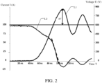
- FIG. 2 is a schematic diagram of voltage overshoot caused by a stray inductance.
- a left longitudinal axis represents a current I, in amperes (A);
- a right longitudinal axis represents a voltage U, in volts (V); and
- a lateral axis represents a time T, in nanoseconds (ns).
- a curve L1 is a voltage change representation, and
- ⁇ V is the instantaneous impulse voltage when the MOSFET device is turned off
- L DC-Link is the stray inductance generated by the copper bar between the bus capacitor C and the terminal of the power module
- L mode is the internal inductance of the power module
- (di/dt) is a switch-on/off speed of the MOSFET device.
- an embodiment of the present disclosure provides a bus capacitor.
- the bus capacitor can be used in an electronic control module of an automobile.
- the electronic control module may be a motor controller.
- the bus capacitor is generally used in cooperation with a power module 700 (such as a power chip, including an IGBT, a SiC MOSFET, or a Si MOSFET).
- FIG. 3 is a schematic structural diagram of a bus capacitor according to an embodiment of the present disclosure.
- FIG. 4 is a schematic structural diagram of the bus capacitor shown in FIG. 3 from another perspective.
- FIG. 5 is a cross-sectional view of the bus capacitor along line A-A in FIG. 3 .
- FIG. 6 is a cross-sectional view of the bus capacitor along line B-B in FIG. 3 .
- FIG. 8 is a schematic structural diagram of cooperation between the bus capacitor and a power module.
- the bus capacitor provided in an embodiment of the present disclosure includes: an insulation housing 600, multiple capacitor layers, and a dielectric 300. Both the multiple capacitor layers and the dielectric 300 are located inside the insulation housing 600.
- the multiple capacitor layers are stacked along a thickness direction (that is, a Z-axis direction) of the bus capacitor, and the dielectric 300 is filled between every two adjacent capacitor layers.
- the insulation housing 600 may be made of plastics.
- the dielectric 300 may be any one of mica, ceramics, and an organic film.
- the insulation housing 600 has a function of protecting the capacitor layers and the dielectric 300, preventing the capacitor layers and the dielectric 300 from getting damp, and so on.
- the insulation housing 600 may be made into a cylindrical shape, a rectangular parallelepiped shape, a cube shape, an elliptical cylinder shape, and the like according to actual needs. This is not limited in the present disclosure.
- the bus capacitor may further include terminals.
- the bus capacitor further includes a positive input terminal 500, a negative input terminal 510, a positive output terminal 520, and a negative output terminal 530.
- the positive input terminal 500 and the negative input terminal 510 serve as input ports for electric energy, and are usually connected to a power supply point inside a controller through a copper bar.
- the positive output terminal 520 and the negative output terminal 530 are respectively connected to a positive connection terminal and a negative connection terminal of the power module 700.
- positive capacitor layers connected to the positive input terminal and the positive output terminal are a same positive capacitor layer, but the positive input terminal and the positive output terminal are connected to different parts of the positive capacitor layer, so that the positive capacitor layer also has an electric energy transmission function.
- the negative input terminal and the negative output terminal are connected to different parts of a same negative capacitor layer, so that the negative capacitor layer also has an electric energy transmission function.
- multiple groups of output terminals may be set. As shown in the figure, three groups of output terminals may be set, and each group of output terminals include one positive output terminal 520 and one negative output terminal 530. Each group of output terminals may be correspondingly connected to one power module 700.
- the positive input terminal 500 and the positive output terminals 520 are distributed in a row, and the negative input terminal 510 and the negative output terminals 530 are distributed in a row, to facilitate the arrangement.
- the positive input terminal 500 and the positive output terminal 520 are diagonally distributed, and the negative input terminal 510 and the negative output terminal 530 are diagonally distributed.
- a connection line between the positive input terminal 500 and the positive output terminal 520 intersects a connection line between the negative input terminal 510 and the negative output terminal 530. In this way, positive and negative currents may be cross-distributed, thereby reducing the inductance.
- the positive input terminal 500 and the positive output terminal 520 are connected to the positive capacitor layer 100, and the negative input terminal 510 and the negative output terminal 530 are connected to the negative capacitor layer 200.
- the multiple capacitor layers include multiple positive capacitor layers 100 and multiple negative capacitor layers 200. More specifically, the multiple positive capacitor layers 100 include a first positive electrode layer 110 and a second positive electrode layer 120. A thickness of the first positive electrode layer 110 is greater than a thickness of the second positive electrode layer 120.
- the multiple negative capacitor layers 200 include a first negative electrode layer 210 and a second negative electrode layer 220. A thickness of the first negative electrode layer 210 is greater than a thickness of the second negative electrode layer 220.
- the positive input terminal 500 is set to be in contact with the first positive electrode layer 110, to enable the positive input terminal 500 to be electrically connected to the first positive electrode layer 110.
- the negative input terminal 510 is set to be in contact with the first negative electrode layer 210 to enable the negative input terminal 510 to be electrically connected to the first negative electrode layer 210.
- the positive output terminal 520 is set to be in contact with the multiple positive capacitor layers 100 to enable the positive output terminal 520 to be electrically connected to the multiple positive capacitor layers 100, that is, to enable both the first positive electrode layer 110 and the second positive electrode layer 120 to be connected to the positive output terminal 520.
- the negative output terminal 530 is set to be connected to the multiple negative capacitor layers 200 to enable the negative output terminal 530 to be electrically connected to the multiple negative capacitor layers 200, that is, to enable both the first negative electrode layer 210 and the second negative electrode layer 220 to be connected to the negative output terminal 530.
- the positive input terminal 500 is connected only to the first positive electrode layer 110
- the negative input terminal 510 is connected only to the first negative electrode layer 210
- the positive output terminal 520 is connected to both the first positive electrode layer 110 and the second positive electrode layer 120
- the negative output terminal 530 is connected to both the first negative electrode layer 210 and the second negative electrode layer 220.
- a load current may be transmitted between the first positive electrode layer 110 and the first negative electrode layer 210, while the second positive electrode layer 120 and the second negative electrode layer 220 only allows a ripple current to flow through, without participating in the transmission of the load current.
- the load current is far greater than the ripple current. Therefore, the first positive electrode layer 110 and the first negative electrode layer 210 are set relatively thick and can well transmit the load current.
- the second positive electrode layer 120 and the second negative electrode layer 220 are set relatively thin, so that resources can be saved, a thickness of the bus capacitor can be reduced, and the ripple current can well flow through.
- the first positive electrode layer 110 and the first negative electrode layer 210 are mainly responsible for transmitting a current, and their thicknesses and quantities of layers may be designed according to a load current that actually needs to be transmitted.
- the second positive electrode layer 120 and the second negative electrode layer 220 that serve as parts providing a main capacitance value, multiple layers of second positive electrode layers 120 and multiple layers of second negative electrode layers 220 may be set to meet a capacitance requirement.
- the positive input terminal 500 may alternatively be set to be connected not only to the first positive electrode layer 110, but also to the second positive electrode layer 120.
- the negative input terminal 510 is set to be connected not only to the first negative electrode layer 210, but also to the second negative electrode layer 220. In this way, the positive input terminal 500 and the negative input terminal 510 may also participate in transmitting the load current, thereby increasing the load of the bus capacitor.
- the first positive electrode layers 110 and the first negative electrode layers 210 have equal quantities of layers, and both can be set to be one layer or at least two layers.
- the second positive electrode layers 120 and the second negative electrode layers 220 have equal quantities of layers, and both can be set to be one layer or at least two layers.
- the multiple capacitor layers may be stacked in any manner.
- the first positive electrode layer 110 and the first negative electrode layer 210 are provided on the topmost layer or the bottom layer; and the first positive electrode layer 110 and the first negative electrode layer 210 are provided on intermediate layers; and so on.
- Some types are listed as follows: First type: stacked from top to bottom are sequentially the first positive electrode layer 110, the first negative electrode layer 210, the second positive electrode layer 120, the second negative electrode layer 220, the second positive electrode layer 120, the second negative electrode layer 220, the second positive electrode layer 120, and the second negative electrode layer 220.
- Second type stacked from top to bottom are sequentially the first negative electrode layer 210, the first positive electrode layer 110, the second positive electrode layer 120, the second negative electrode layer 220, the second positive electrode layer 120, the second negative electrode layer 220, the second positive electrode layer 120, and the second negative electrode layer 220.
- Third type the first positive electrode layer 110, the first negative electrode layer 210, the first positive electrode layer 110, the first negative electrode layer 210, the second positive electrode layer 120, the second negative electrode layer 220, the second positive electrode layer 120, and the second negative electrode layer 220.
- Fourth type stacked from top to bottom are sequentially the first positive electrode layer 110, the first negative electrode layer 210, the second positive electrode layer 120, the second positive electrode layer 120, the second negative electrode layer 220, the second negative electrode layer 220, the second positive electrode layer 120, and the second negative electrode layer 220. Only a few types are listed above, and other similar methods are not enumerated.
- the thicknesses and quantities of layers of the first positive electrode layers 110, the first negative electrode layers 210, the second positive electrode layers 120, and the second negative electrode layers 220 may all be set according to actual needs, which are not limited in the present disclosure.
- FIG. 7 is a schematic structural diagram of the bus capacitor provided with a first conductive member and a second conductive member shown in FIG. 3 .
- the bus capacitor in order to reduce the stray inductance, is provided with a first hole extending along the thickness direction thereof. The first hole runs through the multiple positive capacitor layers 100.
- a first conductive member 400 is provided in the first hole. The first conductive member 400 is in contact with the multiple positive capacitor layers 100, to enable the multiple positive capacitor layers 100 to be electrically connected.
- the bus capacitor is provided with a second hole extending along the thickness direction thereof. The second hole runs through the multiple negative capacitor layers 200.
- a second conductive member 410 is provided in the second hole. The second conductive member 410 is in contact with the multiple negative capacitor layers 200, to enable the multiple negative capacitor layers 200 to be electrically connected.
- the multiple positive capacitor layers 100 may be electrically connected through the first conductive member 400, and the multiple negative capacitor layers 200 may be electrically connected through the second conductive member 410.
- the power module 700 is connected to the bus capacitor through the positive output terminal 520 and the negative output terminal 530, a connection distance between each of the positive capacitor layers 100 and the power module 700 is greatly reduced; and a connection distance between each of the negative capacitor layers 200 and the power module 700 is greatly reduced.
- the distance between the bus capacitor and each of the positive output terminal 520 and the negative output terminal 530 is greatly reduced.
- the capacitor layer may have some resistances, which may cause loss of the transmitted electric energy. Therefore, setting the multiple positive capacitor layers 100 to be electrically connected through the first conductive member 400 and setting the multiple negative capacitor layers 200 to be electrically connected through the second conductive member 410 can further reduce an equivalent series resistance. Specifically, when electric energy is transmitted between relatively thin capacitor layers, resistances of the relatively thin capacitor layers are relatively large, which may cause great loss to the transmitted electric energy.
- the first conductive member 400 connects a thinner second positive electrode layer 120 and a thicker first positive electrode layer 110
- the second conductive member 410 connects a thinner second negative electrode layer 220 and a thicker second positive electrode layer 120.
- first conductive members 400 there may be one or at least two first conductive members 400, and multiple first conductive members 400 may be distributed at different positions to connect different parts of the multiple positive capacitor layers 100. In this way, the equivalent resistance of each part of the thinner positive capacitor layer 100 can be effectively reduced.
- second conductive members 410 there may be one or at least two second conductive members 410, and multiple second conductive members 410 may be distributed at different positions to connect different parts of the multiple negative capacitor layers 200. In this way, the equivalent resistance of each part of the thinner negative capacitor layer 200 can be effectively reduced.
- the first conductive member 400 includes a first conductive rod 402 inserted into the first hole 401.
- the second conductive member 410 includes a second conductive rod 412 inserted into the second hole 411.
- the first conductive rod may be formed of a conductive liquid injected into the first hole, or may be prepared in advance from a conductive material and then inserted into the first hole; or may be made by using an electroless copper plating process. This is not limited in this embodiment. The same applies to the second conductive rod, and details are not described again.
- This type of first conductive member 400 and second conductive member 410 have strong electrical connection stability and are easy to process.
- the first conductive member 400 includes a first conductive layer coated on an inner wall of the first hole
- the second conductive member 410 includes a second conductive layer coated on an inner wall of the second hole. That is, the conductive material is coated on the inner wall of the first hole to form the first conductive member 400, and the conductive material is coated on the inner wall of the second hole to form the second conductive member 410.
- the first conductive member 400 and the second conductive member 410 can have good electrical connection stability with fewer materials consumed and are easy to process, which is beneficial to the lightweight design of the bus capacitor.
- the multiple positive capacitor layers 100 and the multiple negative capacitor layers 200 may be alternately stacked along the thickness direction.
- the first hole when running through the positive capacitor layers 100, the first hole also runs through the negative capacitor layer 200 sandwiched between two adjacent positive capacitor layers 100.
- the first conductive member 400 may be isolated from the negative capacitor layer 200 through which the first hole runs.
- a hole is formed at a position of the negative capacitor layer 200 through which the first hole runs. In this case, this hole may be set relatively large, that is, an aperture of this hole is greater than that of the first hole. In this way, the first conductive member 400 located in the first hole is isolated from the negative capacitor layer 200.
- the second hole further runs through the positive capacitor layer 100 sandwiched between any two adjacent negative capacitor layers 200. Therefore, to prevent the second conductive member 410 in the second hole from coming into contact with the positive capacitor layer 100 and causing a short circuit, the second conductive member 410 may be isolated from the positive capacitor layer 100 through which the first hole runs. Specifically, a hole is formed at a position of the negative capacitor layer 200 through which the second hole runs. In this case, this hole may be set relatively large, that is, an aperture of this hole is greater than that of the second hole. In this way, the second conductive member 410 located in the second hole is isolated from the positive capacitor layer 100.
- a specific structure of the positive input terminal 500 is as follows: The positive input terminal 500 runs through the bus capacitor along the thickness direction, and two opposite ends of the positive input terminal 500 along the thickness direction are exposed outside the insulation housing 600.
- a specific structure of the negative input terminal 510 is as follows: The negative input terminal 510 runs through the bus capacitor along the thickness direction, and two opposite ends of the negative input terminal 510 along the thickness direction are exposed outside the insulation housing 600.
- a positive input hole 501 is provided running through the positive input terminal 500 along the thickness direction.
- a negative input hole 511 is provided running through the negative input terminal 510 along the thickness direction.
- a structure of the positive output terminal 520 is as follows: The positive output terminal 520 runs through the bus capacitor along the thickness direction, and two opposite ends of the positive output terminal 520 along the thickness direction are exposed outside the insulation housing 600.
- a structure of the negative output terminal 530 is as follows: The negative output terminal 530 runs through the bus capacitor along the thickness direction, and two opposite ends of the negative output terminal 530 along the thickness direction are exposed outside the insulation housing 600.
- a positive output hole 521 is provided running through the positive output terminal 520 along the thickness direction.
- a negative output hole 531 is provided running through the negative output terminal 530 along the thickness direction.
- a positive connection terminal 710 of the power module 700 is a positive terminal hole provided in the power module 700
- a negative connection terminal 720 of the power module 700 is a negative terminal hole provided in the power module 700.
- a conductive fastening rod 730 is inserted into the positive output hole 521 and the positive terminal hole.
- the positive terminal hole may be a threaded hole
- the conductive fastening rod 730 may be a fastening bolt. The fastening bolt is tightened in the threaded hole to connect the power module 700 to the bus capacitor.
- the negative terminal hole may be a threaded hole
- the conductive fastening rod 730 may be a fastening bolt.
- the fastening bolt is tightened in the threaded hole to connect the power module 700 to the bus capacitor. In this way, both mechanical connection and electrical connection can be achieved, and the power module 700 and the bus capacitor are in zero-distance contact. This can reduce a stray inductance, thereby relieving impact of the stray inductance on components, allowing an advantage of a fast switch-on/off speed of an MOSFET to be fully utilized, that is, allowing performance of SiC for preparing an MOSFET device to be fully utilized.
- FIG. 9 is a schematic structural diagram of a bus capacitor according to another embodiment of the present disclosure.
- FIG. 10 a cross-sectional view of the bus capacitor along line C-C in FIG. 9 .
- Some other embodiments of the present disclosure provide a bus capacitor. Differences between the bus capacitor and the foregoing embodiment lie in that the positive output terminal 520a is in a shape of a curved sheet, and the negative output terminal 530a is in a shape of a curved sheet; and a mounting hole 800 is provided running through the bus capacitor along the thickness direction thereof, and both the positive output terminal 520a and the negative output terminal 530a are provided in the mounting hole 800.
- the positive output terminal 520a and the negative output terminal 530a are located on a same side of the mounting hole 800.
- both the positive output terminal 520a and the negative output terminal 530a may be U-shaped. Using a direction in the figure as a reference, an opening of the output terminal is upward, and one side of the output terminal is connected to a side wall of a mounting hole 800. The side wall of the mounting hole 800 is formed at a position where the capacitor layer and the dielectric 300 are exposed to the mounting hole 800. Certainly, it should be understood that in the side wall of the mounting hole 800, only the positive capacitor layer 100 is exposed at a connection with the positive output terminal 520a, and only the negative capacitor layer 200 is exposed at a connection with the negative output terminal 530a, thereby preventing a short circuit from occurring.
- the power module When the bus capacitor of this structure is connected to the power module, the power module is correspondingly provided with a plug-in rod with a positive connection terminal and a negative connection terminal.
- the plug-in rod is inserted into the mounting hole 800, and the positive connection terminal abuts against the positive output terminal and the negative connection terminal abuts against the negative output terminal. This enables zero-distance electrical connection between the bus capacitor and the power module to reduce the stray inductance.
- the positive output terminals 520a and the negative output terminals 530a are located on the same side of the mounting hole 800. Therefore, correspondingly, the positive connection terminals and the negative connection terminals may be distributed along a direction of a same side of the mounting hole 800 of the bus capacitor, that is, a width direction of the bus capacitor in the figure. This facilitates the arrangement of the positive output terminals 520a and the negative output terminals 530a.
- FIG. 11 is a schematic structural diagram of a bus capacitor according to still another embodiment of the present disclosure.
- FIG. 12 is a schematic structural diagram of cooperation between the bus capacitor shown in FIG. 11 and a power module.
- Still other embodiments of the present disclosure provide a bus capacitor. Differences between this bus capacitor and the bus capacitor provided in the foregoing embodiment lie in that the positive output terminal 520a and the negative output terminal 530a are located on different sides of the mounting hole 800. It can be seen from the figure that, the positive output terminal 520a is located on a right side of the mounting hole 800, and the negative output terminal 530a is located on a left side of the mounting hole 800.
- the positive connection terminal 710a and the negative connection terminal 720a may be distributed along directions of two sides of the mounting hole 800 of the bus capacitor, that is, a length direction of the bus capacitor in the figure.
- the positive output terminal 520a and the negative output terminal 530a can tightly clamp a plug-in rod of the power module 700 to achieve mechanical connection and electrical connection, with a sample and reliable structure and strong stability.
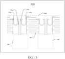
- FIG. 13 is a schematic structural diagram of an automobile according to an embodiment of the present disclosure.
- the automobile includes the bus capacitor described above and at least one power module coupled to the bus capacitor.
- the power module is provided with a positive connection terminal and a negative connection terminal.
- the positive connection terminal is connected to the positive capacitor layer of the bus capacitor.
- the negative connection terminal is connected to the negative capacitor layer of the bus capacitor.
- FIG. 13 only exemplarily shows the cooperation between the bus capacitor and the power module in the automobile. In the present disclosure, other forms of cooperation between the bus capacitor and the power module in the automobile may be further obtained according to other types of structures of the bus capacitor. Details are not described herein.
Landscapes
- Engineering & Computer Science (AREA)
- Power Engineering (AREA)
- Microelectronics & Electronic Packaging (AREA)
- Manufacturing & Machinery (AREA)
- Fixed Capacitors And Capacitor Manufacturing Machines (AREA)
- Inverter Devices (AREA)
- Ceramic Capacitors (AREA)
Abstract
Description
- The present disclosure claims priority to
Chinese Patent Application No. 202110945614.7, filed on August 17, 2021 - The present disclosure relates to a bus capacitor and an automobile.
- The third generation semiconductor represented by silicon carbide (SiC) has excellent performance in the electronic control of new energy vehicles, and has advantages of wide bandgap, high thermal conductivity, high melting point, high critical breakdown electric field, high saturation electron migration speed, and the like. A metal-oxide-semiconductor field-effect transistor (MOSFET) made from SiC has excellent properties such as a low on-resistance, a fast switch-on/off speed, high temperature resistance, and high voltage resistance.
- In a motor drive power module of the new energy vehicle, an MOSFET device made from SiC serves as a switch device. This can reduce losses, improve an endurance mileage of the New European Driving Cycle (NEDC), reduce a volume, and increase space utilization. Currently, because a stray inductance of a system cannot be well controlled, in order to prevent an impact voltage caused by a stray inductance from damaging components during switching on/off, the impact of the stray inductance on the components can be alleviated only by reducing a switch-on/off speed. However, after the switch-on/off is reduced, the advantage of the fast switch-on/off speed of the MOSFET cannot be fully exerted. More specifically, the performance of SiC for preparing the MOSFET device cannot be fully exerted.
- An objective of the present disclosure is to provide a bus capacitor and an automobile, which can reduce a stray inductance, thereby relieving impact of the stray inductance on components, allowing an advantage of a fast switch-on/off speed of an MOSFET to be fully utilized, that is, allowing performance of SiC for preparing an MOSFET device to be fully utilized.
- A first aspect of the present disclosure provides a bus capacitor. The bus capacitor includes: multiple capacitor layers stacked along a thickness direction of the bus capacitor. A dielectric is filled between any two adjacent capacitor layers. The multiple capacitor layers include multiple positive capacitor layers and multiple negative capacitor layers. The bus capacitor is provided with a first hole extending along the thickness direction thereof. The first hole runs through the multiple positive capacitor layers. A first conductive member is provided in the first hole. The first conductive member is in contact with the multiple positive capacitor layers, to enable the multiple positive capacitor layers to be electrically connected. The bus capacitor is provided with a second hole extending along the thickness direction thereof. The second hole runs through the multiple negative capacitor layers. A second conductive member is provided in the second hole. The second conductive member is in contact with the multiple negative capacitor layers, to enable the multiple negative capacitor layers to be electrically connected.
- In some embodiments, the first conductive member includes a first conductive rod inserted into the first hole. The second conductive member includes a second conductive rod inserted into the second hole.
- In some embodiments, the first conductive member includes a first conductive layer coated on an inner wall of the first hole. The second conductive member includes a second conductive layer coated on an inner wall of the second hole.
- In some embodiments, the multiple positive capacitor layers and the multiple negative capacitor layers are alternately stacked along the thickness direction. The first hole further runs through the negative capacitor layer. The negative capacitor layer is sandwiched between any two adjacent positive capacitor layers. The first conductive member is isolated from the negative capacitor layer through which the first hole runs. The second hole further runs through the positive capacitor layer. The positive capacitor layer is sandwiched between any two adjacent negative capacitor layers. The second conductive member is isolated from the positive capacitor layer through which the second hole runs.
- In some embodiments, the bus capacitor is provided with multiple first holes extending along the thickness direction thereof. The bus capacitor is provided with multiple second holes extending along the thickness direction thereof. Multiple first conductive members in the multiple first holes are distributed at different positions to electrically connect different parts of the multiple positive capacitor layers. Multiple second conductive members in the multiple second holes are distributed at different positions to electrically connect different parts of the multiple negative capacitor layers.
- In some embodiments, the multiple positive capacitor layers include a first positive electrode layer and a second positive electrode layer. A thickness of the first positive electrode layer is greater than a thickness of the second positive electrode layer. The multiple negative capacitor layers include a first negative electrode layer and a second negative electrode layer. A thickness of the first negative electrode layer is greater than a thickness of the second negative electrode layer.
- In some embodiments, the bus capacitor further includes a positive input terminal, a negative input terminal, a positive output terminal, and a negative output terminal. The positive input terminal is in contact with the first positive electrode layer to cause the positive input terminal to be electrically connected to the first positive electrode layer. The negative input terminal is in contact with the first negative electrode layer to cause the negative input terminal to be electrically connected to the first negative electrode layer. The positive output terminal is in contact with the multiple positive capacitor layers to cause the positive output terminal to be electrically connected to the multiple positive capacitor layers. The negative output terminal is in contact with the multiple negative capacitor layers to cause the negative output terminal to be electrically connected to the multiple negative capacitor layers.
- In some embodiments, the bus capacitor further includes an insulation housing. The multiple capacitor layers are provided inside the insulation housing. The positive input terminal runs through the bus capacitor along the thickness direction. Two opposite ends of the positive input terminal along the thickness direction are exposed outside the insulation housing. The negative input terminal runs through the bus capacitor along the thickness direction. Two opposite ends of the negative input terminal along the thickness direction are exposed outside the insulation housing. A positive input hole is provided running through the positive input terminal along the thickness direction. A negative input hole is provided running through the negative input terminal along the thickness direction.
- In some embodiments, the bus capacitor further includes an insulation housing. The multiple capacitor layers are provided inside the insulation housing. The positive output terminal runs through the bus capacitor along the thickness direction. Two opposite ends of the positive output terminal along the thickness direction are exposed outside the insulation housing. The negative output terminal runs through the bus capacitor along the thickness direction. Two opposite ends of the negative output terminal along the thickness direction are exposed outside the insulation housing. A positive output hole is provided running through the positive output terminal along the thickness direction. A negative output hole is provided running through the negative output terminal along the thickness direction.
- In some other embodiments, the bus capacitor further includes an insulation housing. The multiple capacitor layers are provided inside the insulation housing. The positive output terminal is in a shape of a curved sheet. The negative output terminal is in a shape of a curved sheet. A mounting hole is provided running through the bus capacitor along the thickness direction thereof. Both the positive output terminal and the negative output terminal are provided inside the mounting hole. The positive output terminal and the negative output terminal are located on a same side or on different sides of the mounting hole.
- In some embodiments, a connection line between the positive input terminal and the positive output terminal intersects a connection line between the negative input terminal and the negative output terminal.
- In some embodiments, the multiple positive capacitor layers include multiple second positive electrode layers. The multiple negative capacitor layers include multiple second negative electrode layers. A number of layers of the second positive electrode layers is equal to a number of layers of the second negative electrode layers.
- In some embodiments, the bus capacitor further includes a positive input terminal and a negative input terminal. The positive input terminal is electrically connected to the first positive electrode layer and the second positive electrode layer. The negative input terminal is electrically connected to the first negative electrode layer and the second negative electrode layer.
- A second aspect of the present disclosure provides an automobile. The automobile includes: the bus capacitor according to any item of the first aspect of the present disclosure and a power module. The power module is provided with a positive connection terminal and a negative connection terminal. The positive connection terminal is connected to the positive capacitor layer of the bus capacitor. The negative connection terminal is connected to the negative capacitor layer of the bus capacitor.
- According to the bus capacitor provided in the present disclosure, multiple positive capacitor layers of the bus capacitor may be electrically connected through the first conductive member provided in the first hole extending along the thickness direction of the bus capacitor and running through the multiple positive capacitor layers, and multiple negative capacitor layers of the bus capacitor may be electrically connected through the second conductive member provided in the second hole extending along the thickness direction of the bus capacitor and running through the multiple negative capacitor layers. In this way, when the power module is connected to the bus capacitor through the positive output terminal and the negative output terminal, a connection distance between each positive capacitor layer and the power module is greatly shortened; and a connection distance between each negative capacitor layer and the power module is also greatly shortened. This can reduce a stray inductance, and relieve impact of the stray inductance on components, thereby allowing an advantage of a fast switch-on/off speed of an MOSFET to be fully utilized, that is, allowing performance of SiC for preparing an MOSFET device to be fully utilized.
- Details of one or more embodiments of the present disclosure are provided in the accompanying drawings and descriptions below. Other features and advantages of the present disclosure become obvious with reference to the specification, the accompanying drawings, and the claims.
- To describe the technical solutions in the present disclosure more clearly, the following briefly introduces the accompanying drawings required in the specific implementations.
-
FIG. 1 is a schematic diagram of the principle of generating a stray inductance; -
FIG. 2 is a schematic diagram of voltage overshoot caused by a stray inductance; -
FIG. 3 is a schematic structural diagram of a bus capacitor according to an embodiment of the present disclosure; -
FIG. 4 is a schematic structural diagram of the bus capacitor shown inFIG. 3 from another perspective; -
FIG. 5 is a cross-sectional view of the bus capacitor along line A-A inFIG. 3 ; -
FIG. 6 is a cross-sectional view of the bus capacitor along line B-B inFIG. 3 ; -
FIG. 7 is a schematic structural diagram of the bus capacitor provided with a first conductive member and a second conductive member shown inFIG. 3 ; -
FIG. 8 is a schematic structural diagram of cooperation between the bus capacitor and a power module; -
FIG. 9 is a schematic structural diagram of a bus capacitor according to another embodiment of the present disclosure; -
FIG. 10 a cross-sectional view of the bus capacitor along line C-C inFIG. 9 ; -
FIG. 11 is a schematic structural diagram of a bus capacitor according to still another embodiment of the present disclosure; -
FIG. 12 is a schematic structural diagram of cooperation between the bus capacitor shown inFIG. 11 and a power module; and -
FIG. 13 is a schematic structural diagram of an automobile according to an embodiment of the present disclosure. - Description of reference numerals: 1000-bus capacitor, 100-positive capacitor layer, 110-first positive electrode layer, 120-second positive electrode layer, 200-negative capacitor layer, 210-first negative electrode layer, 220-second negative electrode layer, 300-dielectric, 400-first conductive member, 401-first hole, 402-first conductive rod, 403-first conductive layer, 410-second conductive member, 411-second hole, 412-second conductive rod, 413-second conductive layer, 500-positive input terminal, 501-positive input hole, 510-negative input terminal, 511-negative input hole, 520, 520a-positive output terminal, 521-positive output hole, 530, 530a-negative output terminal, 531-negative output hole, 600-insulation housing, 700-power module, 710, 710a-positive connection terminal, 720, 720a-negative connection terminal, 730-conductive fastening rod, 800-mounting hole, 2000-automobile.
- The following clearly and completely describes the technical solutions in the embodiments of the present disclosure with reference to the accompanying drawings in the embodiments of the present disclosure.
- In this specification and the claims of the present disclosure, the terms "first", "second", and so on are intended to distinguish similar objects, but do not necessarily indicate a specific order or sequence. It should be understood that the data termed in such a way is interchangeable in proper circumstances, so that the embodiments of the present disclosure can be implemented in other sequences than the sequence illustrated or described herein. In addition, the objects distinguished by "first", "second", and the like are usually of one type, and there is no limitation on quantities of the objects. For example, there may be one or more first objects.
- In the present disclosure, unless otherwise explicitly specified or defined, the terms such as "connect" should be understood in a broad sense. For example, the connection may be a fixed connection, a detachable connection, or an integral connection; or the connection may be a mechanical connection or an electrical connection; or the connection may be a direct connection, an indirect connection through an intermediary, internal communication between two components, or an interaction relationship between two components. A person of ordinary skill in the art may understand the specific meanings of the foregoing terms in the present disclosure according to specific situations.
- In the present disclosure, unless otherwise explicitly specified or defined, the first feature being located "above" or "below" the second feature may be the first feature being in a direct contact with the second feature, or the first feature being in an indirect contact with the second feature through an intermediary. In addition, that the first feature is "above", "over", or "on" the second feature may indicate that the first feature is directly above or obliquely above the second feature, or may merely indicate that the horizontal position of the first feature is higher than that of the second feature. That the first feature is "below", "under", and "beneath" the second feature may be that the first feature is right below the second feature or at an inclined bottom of the second feature, or may merely indicate that the horizontal position of the first feature is lower than that of the second feature.
-
FIG. 1 is a schematic diagram of the principle of generating a stray inductance. The stray inductance includes two parts. One part is a stray inductance generated by a copper bar between a bus capacitor C and a terminal of apower module 700. This part of stray inductance is represented by LDC-Link inFIG. 1 . The other part is an internal inductance of the power module and represented by Lmode inFIG. 1 . Certainly, it can be understood that, the power module as a whole is a direct current to alternating current (DC-AC) conversion module, such as a DC-AC converter. Two MOSFET devices are provided in the power module. A node A between the two MOSFETs is an output terminal of the power module. Generally, inFIG. 1 , an upper MOSFET device is connected to a positive electrode of the capacitor C after being turned on, a lower MOSFET device is connected to a negative electrode of the capacitor C after being turned on, and the upper MOSFET and the lower MOSFET are alternately turned on, thereby converting DC to AC. -
FIG. 2 is a schematic diagram of voltage overshoot caused by a stray inductance. InFIG. 2 , a left longitudinal axis represents a current I, in amperes (A); a right longitudinal axis represents a voltage U, in volts (V); and a lateral axis represents a time T, in nanoseconds (ns). A curve L1 is a voltage change representation, and a curve L2 is a current change representation. It can be seen fromFIG. 2 that, after power is off, an instantaneous impulse voltage is ΔV , where ΔV is calculated by using the following formula:
- In formula 1, ΔV is the instantaneous impulse voltage when the MOSFET device is turned off, LDC-Link is the stray inductance generated by the copper bar between the bus capacitor C and the terminal of the power module, Lmode is the internal inductance of the power module, and (di/dt) is a switch-on/off speed of the MOSFET device. It can be seen from formula 1 that, when the stray inductance Lmode remains unchanged, a larger stray inductance LDC-Link indicates a larger instantaneous impulse voltage ΔV . If the stray inductance LDC-Link cannot be reduced, in order to prevent the instantaneous impulse voltage ΔV from being too large, the switch-on/off speed (di/dt) of the MOSFET device needs to be controlled to be reduced.
- However, reducing the switch-on/off speed of the MOSFET device hinders the full exertion of the advantage of the MOSFET device (that is, the fast switch-on/off speed). More specifically, the performance of SiC for preparing the MOSFET device cannot be fully exerted.
- To resolve the foregoing problem, an embodiment of the present disclosure provides a bus capacitor. The bus capacitor can be used in an electronic control module of an automobile. The electronic control module may be a motor controller. Certainly, it should be understood that, the bus capacitor is generally used in cooperation with a power module 700 (such as a power chip, including an IGBT, a SiC MOSFET, or a Si MOSFET).
- Refer to
FIG. 3 to FIG. 6 , andFIG. 8 .FIG. 3 is a schematic structural diagram of a bus capacitor according to an embodiment of the present disclosure.FIG. 4 is a schematic structural diagram of the bus capacitor shown inFIG. 3 from another perspective.FIG. 5 is a cross-sectional view of the bus capacitor along line A-A inFIG. 3 .FIG. 6 is a cross-sectional view of the bus capacitor along line B-B inFIG. 3 .FIG. 8 is a schematic structural diagram of cooperation between the bus capacitor and a power module. The bus capacitor provided in an embodiment of the present disclosure includes: aninsulation housing 600, multiple capacitor layers, and a dielectric 300. Both the multiple capacitor layers and the dielectric 300 are located inside theinsulation housing 600. The multiple capacitor layers are stacked along a thickness direction (that is, a Z-axis direction) of the bus capacitor, and the dielectric 300 is filled between every two adjacent capacitor layers. - The
insulation housing 600 may be made of plastics. The dielectric 300 may be any one of mica, ceramics, and an organic film. Theinsulation housing 600 has a function of protecting the capacitor layers and the dielectric 300, preventing the capacitor layers and the dielectric 300 from getting damp, and so on. Theinsulation housing 600 may be made into a cylindrical shape, a rectangular parallelepiped shape, a cube shape, an elliptical cylinder shape, and the like according to actual needs. This is not limited in the present disclosure. - A person skilled in the art needs to understand that the bus capacitor ultimately needs to be connected to the
power module 700, and therefore, the bus capacitor may further include terminals. Specifically, the bus capacitor further includes apositive input terminal 500, anegative input terminal 510, apositive output terminal 520, and anegative output terminal 530. Thepositive input terminal 500 and thenegative input terminal 510 serve as input ports for electric energy, and are usually connected to a power supply point inside a controller through a copper bar. Thepositive output terminal 520 and thenegative output terminal 530 are respectively connected to a positive connection terminal and a negative connection terminal of thepower module 700. - It should be understood that, in this embodiment, positive capacitor layers connected to the positive input terminal and the positive output terminal are a same positive capacitor layer, but the positive input terminal and the positive output terminal are connected to different parts of the positive capacitor layer, so that the positive capacitor layer also has an electric energy transmission function. Similarly, the negative input terminal and the negative output terminal are connected to different parts of a same negative capacitor layer, so that the negative capacitor layer also has an electric energy transmission function.
- In this embodiment, multiple groups of output terminals may be set. As shown in the figure, three groups of output terminals may be set, and each group of output terminals include one
positive output terminal 520 and onenegative output terminal 530. Each group of output terminals may be correspondingly connected to onepower module 700. - In some specific implementations, the
positive input terminal 500 and thepositive output terminals 520 are distributed in a row, and thenegative input terminal 510 and thenegative output terminals 530 are distributed in a row, to facilitate the arrangement. - In some other specific implementations, the
positive input terminal 500 and thepositive output terminal 520 are diagonally distributed, and thenegative input terminal 510 and thenegative output terminal 530 are diagonally distributed. A connection line between thepositive input terminal 500 and thepositive output terminal 520 intersects a connection line between thenegative input terminal 510 and thenegative output terminal 530. In this way, positive and negative currents may be cross-distributed, thereby reducing the inductance. - During internal connection, the
positive input terminal 500 and thepositive output terminal 520 are connected to thepositive capacitor layer 100, and thenegative input terminal 510 and thenegative output terminal 530 are connected to thenegative capacitor layer 200. - Specifically, the multiple capacitor layers include multiple
positive capacitor layers 100 and multiple negative capacitor layers 200. More specifically, the multiplepositive capacitor layers 100 include a firstpositive electrode layer 110 and a secondpositive electrode layer 120. A thickness of the firstpositive electrode layer 110 is greater than a thickness of the secondpositive electrode layer 120. The multiplenegative capacitor layers 200 include a firstnegative electrode layer 210 and a secondnegative electrode layer 220. A thickness of the firstnegative electrode layer 210 is greater than a thickness of the secondnegative electrode layer 220. - In some specific implementations, the
positive input terminal 500 is set to be in contact with the firstpositive electrode layer 110, to enable thepositive input terminal 500 to be electrically connected to the firstpositive electrode layer 110. Thenegative input terminal 510 is set to be in contact with the firstnegative electrode layer 210 to enable thenegative input terminal 510 to be electrically connected to the firstnegative electrode layer 210. - The
positive output terminal 520 is set to be in contact with the multiplepositive capacitor layers 100 to enable thepositive output terminal 520 to be electrically connected to the multiplepositive capacitor layers 100, that is, to enable both the firstpositive electrode layer 110 and the secondpositive electrode layer 120 to be connected to thepositive output terminal 520. Thenegative output terminal 530 is set to be connected to the multiplenegative capacitor layers 200 to enable thenegative output terminal 530 to be electrically connected to the multiplenegative capacitor layers 200, that is, to enable both the firstnegative electrode layer 210 and the secondnegative electrode layer 220 to be connected to thenegative output terminal 530. - That is, the
positive input terminal 500 is connected only to the firstpositive electrode layer 110, thenegative input terminal 510 is connected only to the firstnegative electrode layer 210, thepositive output terminal 520 is connected to both the firstpositive electrode layer 110 and the secondpositive electrode layer 120, and thenegative output terminal 530 is connected to both the firstnegative electrode layer 210 and the secondnegative electrode layer 220. In this case, a load current may be transmitted between the firstpositive electrode layer 110 and the firstnegative electrode layer 210, while the secondpositive electrode layer 120 and the secondnegative electrode layer 220 only allows a ripple current to flow through, without participating in the transmission of the load current. - Generally, the load current is far greater than the ripple current. Therefore, the first
positive electrode layer 110 and the firstnegative electrode layer 210 are set relatively thick and can well transmit the load current. The secondpositive electrode layer 120 and the secondnegative electrode layer 220 are set relatively thin, so that resources can be saved, a thickness of the bus capacitor can be reduced, and the ripple current can well flow through. - In this embodiment, the first
positive electrode layer 110 and the firstnegative electrode layer 210 are mainly responsible for transmitting a current, and their thicknesses and quantities of layers may be designed according to a load current that actually needs to be transmitted. In terms of the secondpositive electrode layer 120 and the secondnegative electrode layer 220 that serve as parts providing a main capacitance value, multiple layers of secondpositive electrode layers 120 and multiple layers of secondnegative electrode layers 220 may be set to meet a capacitance requirement. - In some other specific implementations, the
positive input terminal 500 may alternatively be set to be connected not only to the firstpositive electrode layer 110, but also to the secondpositive electrode layer 120. Correspondingly, thenegative input terminal 510 is set to be connected not only to the firstnegative electrode layer 210, but also to the secondnegative electrode layer 220. In this way, thepositive input terminal 500 and thenegative input terminal 510 may also participate in transmitting the load current, thereby increasing the load of the bus capacitor. - Regardless of the connection method, the first
positive electrode layers 110 and the firstnegative electrode layers 210 have equal quantities of layers, and both can be set to be one layer or at least two layers. The secondpositive electrode layers 120 and the secondnegative electrode layers 220 have equal quantities of layers, and both can be set to be one layer or at least two layers. - It can be understood that, the multiple capacitor layers may be stacked in any manner. For example, the first
positive electrode layer 110 and the firstnegative electrode layer 210 are provided on the topmost layer or the bottom layer; and the firstpositive electrode layer 110 and the firstnegative electrode layer 210 are provided on intermediate layers; and so on. Some types are listed as follows: First type: stacked from top to bottom are sequentially the firstpositive electrode layer 110, the firstnegative electrode layer 210, the secondpositive electrode layer 120, the secondnegative electrode layer 220, the secondpositive electrode layer 120, the secondnegative electrode layer 220, the secondpositive electrode layer 120, and the secondnegative electrode layer 220. Second type: stacked from top to bottom are sequentially the firstnegative electrode layer 210, the firstpositive electrode layer 110, the secondpositive electrode layer 120, the secondnegative electrode layer 220, the secondpositive electrode layer 120, the secondnegative electrode layer 220, the secondpositive electrode layer 120, and the secondnegative electrode layer 220. Third type: the firstpositive electrode layer 110, the firstnegative electrode layer 210, the firstpositive electrode layer 110, the firstnegative electrode layer 210, the secondpositive electrode layer 120, the secondnegative electrode layer 220, the secondpositive electrode layer 120, and the secondnegative electrode layer 220. Fourth type: stacked from top to bottom are sequentially the firstpositive electrode layer 110, the firstnegative electrode layer 210, the secondpositive electrode layer 120, the secondpositive electrode layer 120, the secondnegative electrode layer 220, the secondnegative electrode layer 220, the secondpositive electrode layer 120, and the secondnegative electrode layer 220. Only a few types are listed above, and other similar methods are not enumerated. - The thicknesses and quantities of layers of the first
positive electrode layers 110, the firstnegative electrode layers 210, the secondpositive electrode layers 120, and the secondnegative electrode layers 220 may all be set according to actual needs, which are not limited in the present disclosure. -
FIG. 7 is a schematic structural diagram of the bus capacitor provided with a first conductive member and a second conductive member shown inFIG. 3 . In this embodiment, in order to reduce the stray inductance, the bus capacitor is provided with a first hole extending along the thickness direction thereof. The first hole runs through the multiple positive capacitor layers 100. A first conductive member 400 is provided in the first hole. The first conductive member 400 is in contact with the multiplepositive capacitor layers 100, to enable the multiplepositive capacitor layers 100 to be electrically connected. The bus capacitor is provided with a second hole extending along the thickness direction thereof. The second hole runs through the multiple negative capacitor layers 200. A second conductive member 410 is provided in the second hole. The second conductive member 410 is in contact with the multiplenegative capacitor layers 200, to enable the multiplenegative capacitor layers 200 to be electrically connected. - It can be learned that, in this embodiment, the multiple
positive capacitor layers 100 may be electrically connected through the first conductive member 400, and the multiplenegative capacitor layers 200 may be electrically connected through the second conductive member 410. In this way, when thepower module 700 is connected to the bus capacitor through thepositive output terminal 520 and thenegative output terminal 530, a connection distance between each of thepositive capacitor layers 100 and thepower module 700 is greatly reduced; and a connection distance between each of thenegative capacitor layers 200 and thepower module 700 is greatly reduced. Compared with the conventional method of using a copper bar or a connection line, in the present disclosure, the distance between the bus capacitor and each of thepositive output terminal 520 and thenegative output terminal 530 is greatly reduced. This can reduce the stray inductance, and relieve impact of the stray inductance on components, thereby allowing an advantage of a fast switch-on/off speed of an MOSFET to be fully utilized, that is, allowing performance of SiC for preparing an MOSFET device to be fully utilized. - In addition, the capacitor layer may have some resistances, which may cause loss of the transmitted electric energy. Therefore, setting the multiple
positive capacitor layers 100 to be electrically connected through the first conductive member 400 and setting the multiplenegative capacitor layers 200 to be electrically connected through the second conductive member 410 can further reduce an equivalent series resistance. Specifically, when electric energy is transmitted between relatively thin capacitor layers, resistances of the relatively thin capacitor layers are relatively large, which may cause great loss to the transmitted electric energy. In this case, the first conductive member 400 connects a thinner secondpositive electrode layer 120 and a thicker firstpositive electrode layer 110, and the second conductive member 410 connects a thinner secondnegative electrode layer 220 and a thicker secondpositive electrode layer 120. In this way, when a current is transmitted through the thinner secondpositive electrode layer 120 and secondnegative electrode layer 220, part of the current is shunted to the thicker firstpositive electrode layer 110 and firstnegative electrode layer 210 for transmission. Because the thicker firstpositive electrode layer 110 and firstnegative electrode layer 210 have smaller resistances, the loss during transmission of electric energy is also smaller, which is equivalent to reducing an equivalent series resistance during the transmission of the electric energy. - For example, there may be one or at least two first conductive members 400, and multiple first conductive members 400 may be distributed at different positions to connect different parts of the multiple positive capacitor layers 100. In this way, the equivalent resistance of each part of the thinner
positive capacitor layer 100 can be effectively reduced. Similarly, there may be one or at least two second conductive members 410, and multiple second conductive members 410 may be distributed at different positions to connect different parts of the multiple negative capacitor layers 200. In this way, the equivalent resistance of each part of the thinnernegative capacitor layer 200 can be effectively reduced. - Multiple manners may be used for the first conductive member 400 and second conductive member 410. In some specific implementations, the first conductive member 400 includes a first conductive rod 402 inserted into the first hole 401. The second conductive member 410 includes a second conductive rod 412 inserted into the second hole 411. The first conductive rod may be formed of a conductive liquid injected into the first hole, or may be prepared in advance from a conductive material and then inserted into the first hole; or may be made by using an electroless copper plating process. This is not limited in this embodiment. The same applies to the second conductive rod, and details are not described again. This type of first conductive member 400 and second conductive member 410 have strong electrical connection stability and are easy to process.
- In some other specific implementations, the first conductive member 400 includes a first conductive layer coated on an inner wall of the first hole, and the second conductive member 410 includes a second conductive layer coated on an inner wall of the second hole. That is, the conductive material is coated on the inner wall of the first hole to form the first conductive member 400, and the conductive material is coated on the inner wall of the second hole to form the second conductive member 410. In this way, the first conductive member 400 and the second conductive member 410 can have good electrical connection stability with fewer materials consumed and are easy to process, which is beneficial to the lightweight design of the bus capacitor.
- As mentioned above, the multiple
positive capacitor layers 100 and the multiplenegative capacitor layers 200 may be alternately stacked along the thickness direction. In this case, when running through thepositive capacitor layers 100, the first hole also runs through thenegative capacitor layer 200 sandwiched between two adjacent positive capacitor layers 100. To prevent the first conductive member 400 in the first hole from coming into contact with thenegative capacitor layer 200 and causing a short circuit, the first conductive member 400 may be isolated from thenegative capacitor layer 200 through which the first hole runs. Specifically, a hole is formed at a position of thenegative capacitor layer 200 through which the first hole runs. In this case, this hole may be set relatively large, that is, an aperture of this hole is greater than that of the first hole. In this way, the first conductive member 400 located in the first hole is isolated from thenegative capacitor layer 200. - Similarly, the second hole further runs through the
positive capacitor layer 100 sandwiched between any two adjacent negative capacitor layers 200. Therefore, to prevent the second conductive member 410 in the second hole from coming into contact with thepositive capacitor layer 100 and causing a short circuit, the second conductive member 410 may be isolated from thepositive capacitor layer 100 through which the first hole runs. Specifically, a hole is formed at a position of thenegative capacitor layer 200 through which the second hole runs. In this case, this hole may be set relatively large, that is, an aperture of this hole is greater than that of the second hole. In this way, the second conductive member 410 located in the second hole is isolated from thepositive capacitor layer 100. - In this embodiment, a specific structure of the
positive input terminal 500 is as follows: Thepositive input terminal 500 runs through the bus capacitor along the thickness direction, and two opposite ends of thepositive input terminal 500 along the thickness direction are exposed outside theinsulation housing 600. A specific structure of thenegative input terminal 510 is as follows: Thenegative input terminal 510 runs through the bus capacitor along the thickness direction, and two opposite ends of thenegative input terminal 510 along the thickness direction are exposed outside theinsulation housing 600. Apositive input hole 501 is provided running through thepositive input terminal 500 along the thickness direction. Anegative input hole 511 is provided running through thenegative input terminal 510 along the thickness direction. - In this embodiment, a structure of the
positive output terminal 520 is as follows: Thepositive output terminal 520 runs through the bus capacitor along the thickness direction, and two opposite ends of thepositive output terminal 520 along the thickness direction are exposed outside theinsulation housing 600. A structure of thenegative output terminal 530 is as follows: Thenegative output terminal 530 runs through the bus capacitor along the thickness direction, and two opposite ends of thenegative output terminal 530 along the thickness direction are exposed outside theinsulation housing 600. Apositive output hole 521 is provided running through thepositive output terminal 520 along the thickness direction. Anegative output hole 531 is provided running through thenegative output terminal 530 along the thickness direction. - Regarding the
positive output terminal 520 of this structure and thenegative output terminal 530 of this structure, apositive connection terminal 710 of thepower module 700 is a positive terminal hole provided in thepower module 700, and anegative connection terminal 720 of thepower module 700 is a negative terminal hole provided in thepower module 700. During connection of the bus capacitor and thepower module 700, aconductive fastening rod 730 is inserted into thepositive output hole 521 and the positive terminal hole. The positive terminal hole may be a threaded hole, and theconductive fastening rod 730 may be a fastening bolt. The fastening bolt is tightened in the threaded hole to connect thepower module 700 to the bus capacitor. Similarly, anotherconductive fastening rod 730 is inserted into thenegative output hole 531 and the negative terminal hole. The negative terminal hole may be a threaded hole, and theconductive fastening rod 730 may be a fastening bolt. The fastening bolt is tightened in the threaded hole to connect thepower module 700 to the bus capacitor. In this way, both mechanical connection and electrical connection can be achieved, and thepower module 700 and the bus capacitor are in zero-distance contact. This can reduce a stray inductance, thereby relieving impact of the stray inductance on components, allowing an advantage of a fast switch-on/off speed of an MOSFET to be fully utilized, that is, allowing performance of SiC for preparing an MOSFET device to be fully utilized. - Refer to
FIG. 9 and FIG. 10. FIG. 9 is a schematic structural diagram of a bus capacitor according to another embodiment of the present disclosure.FIG. 10 a cross-sectional view of the bus capacitor along line C-C inFIG. 9 . Some other embodiments of the present disclosure provide a bus capacitor. Differences between the bus capacitor and the foregoing embodiment lie in that thepositive output terminal 520a is in a shape of a curved sheet, and thenegative output terminal 530a is in a shape of a curved sheet; and a mountinghole 800 is provided running through the bus capacitor along the thickness direction thereof, and both thepositive output terminal 520a and thenegative output terminal 530a are provided in the mountinghole 800. In addition, thepositive output terminal 520a and thenegative output terminal 530a are located on a same side of the mountinghole 800. - Specifically, both the
positive output terminal 520a and thenegative output terminal 530a may be U-shaped. Using a direction in the figure as a reference, an opening of the output terminal is upward, and one side of the output terminal is connected to a side wall of a mountinghole 800. The side wall of the mountinghole 800 is formed at a position where the capacitor layer and the dielectric 300 are exposed to the mountinghole 800. Certainly, it should be understood that in the side wall of the mountinghole 800, only thepositive capacitor layer 100 is exposed at a connection with thepositive output terminal 520a, and only thenegative capacitor layer 200 is exposed at a connection with thenegative output terminal 530a, thereby preventing a short circuit from occurring. - When the bus capacitor of this structure is connected to the power module, the power module is correspondingly provided with a plug-in rod with a positive connection terminal and a negative connection terminal. The plug-in rod is inserted into the mounting
hole 800, and the positive connection terminal abuts against the positive output terminal and the negative connection terminal abuts against the negative output terminal. This enables zero-distance electrical connection between the bus capacitor and the power module to reduce the stray inductance. - The
positive output terminals 520a and thenegative output terminals 530a are located on the same side of the mountinghole 800. Therefore, correspondingly, the positive connection terminals and the negative connection terminals may be distributed along a direction of a same side of the mountinghole 800 of the bus capacitor, that is, a width direction of the bus capacitor in the figure. This facilitates the arrangement of thepositive output terminals 520a and thenegative output terminals 530a. - Refer to
FIG. 11 andFIG. 12 .FIG. 11 is a schematic structural diagram of a bus capacitor according to still another embodiment of the present disclosure.FIG. 12 is a schematic structural diagram of cooperation between the bus capacitor shown inFIG. 11 and a power module. Still other embodiments of the present disclosure provide a bus capacitor. Differences between this bus capacitor and the bus capacitor provided in the foregoing embodiment lie in that thepositive output terminal 520a and thenegative output terminal 530a are located on different sides of the mountinghole 800. It can be seen from the figure that, thepositive output terminal 520a is located on a right side of the mountinghole 800, and thenegative output terminal 530a is located on a left side of the mountinghole 800. Correspondingly, thepositive connection terminal 710a and thenegative connection terminal 720a may be distributed along directions of two sides of the mountinghole 800 of the bus capacitor, that is, a length direction of the bus capacitor in the figure. In this way, thepositive output terminal 520a and thenegative output terminal 530a can tightly clamp a plug-in rod of thepower module 700 to achieve mechanical connection and electrical connection, with a sample and reliable structure and strong stability. -
FIG. 13 is a schematic structural diagram of an automobile according to an embodiment of the present disclosure. In some embodiments, the automobile includes the bus capacitor described above and at least one power module coupled to the bus capacitor. The power module is provided with a positive connection terminal and a negative connection terminal. The positive connection terminal is connected to the positive capacitor layer of the bus capacitor. The negative connection terminal is connected to the negative capacitor layer of the bus capacitor. It should be noted that,FIG. 13 only exemplarily shows the cooperation between the bus capacitor and the power module in the automobile. In the present disclosure, other forms of cooperation between the bus capacitor and the power module in the automobile may be further obtained according to other types of structures of the bus capacitor. Details are not described herein. - The embodiments of the present disclosure are described in detail above. Although the principles and specific implementations of the present disclosure are described by using specific examples in this specification, the descriptions of the foregoing embodiments can be intended to help understand the method and the core idea of the method of the present disclosure.
Claims (14)
- A bus capacitor (1000), comprising: a plurality of capacitor layers stacked along a thickness direction of the bus capacitor, a dielectric (300) being filled between any two adjacent capacitor layers; and the plurality of capacitor layers comprising a plurality of positive capacitor layers (100) and a plurality of negative capacitor layers (200);the bus capacitor being provided with a first hole (401) extending along the thickness direction thereof, and the first hole running through the plurality of positive capacitor layers; and a first conductive member (400) being provided in the first hole, and the first conductive member being in contact with the plurality of positive capacitor layers, to enable the plurality of positive capacitor layers to be electrically connected; andthe bus capacitor being provided with a second hole (411) extending along the thickness direction thereof, and the second hole running through the plurality of negative capacitor layers; and a second conductive member (410) being provided in the second hole, and the second conductive member being in contact with the plurality of negative capacitor layers, to enable the plurality of negative capacitor layers to be electrically connected.
- The bus capacitor according to claim 1, wherein the first conductive member comprises a first conductive rod (402) inserted into the first hole; and the second conductive member comprises a second conductive rod (412) inserted into the second hole.
- The bus capacitor according to claim 1, wherein the first conductive member comprises a first conductive layer (403) coated on an inner wall of the first hole, and the second conductive member comprises a second conductive layer (413) coated on an inner wall of the second hole.
- The bus capacitor according to claim 1, wherein the plurality of positive capacitor layers and the plurality of negative capacitor layers are alternately stacked along the thickness direction;the first hole further runs through the negative capacitor layer, the negative capacitor layer is sandwiched between any two adjacent positive capacitor layers, and the first conductive member is isolated from the negative capacitor layer through which the first hole runs; andthe second hole further runs through the positive capacitor layer, the positive capacitor layer is sandwiched between any two adjacent negative capacitor layers, and the second conductive member is isolated from the positive capacitor layer through which the second hole runs.
- The bus capacitor according to claim 1, wherein the bus capacitor is provided with a plurality of first holes extending along the thickness direction thereof; the bus capacitor is provided with a plurality of second holes extending along the thickness direction thereof; a plurality of first conductive members in the plurality of first holes are distributed at different positions to electrically connect different parts of the plurality of positive capacitor layers; and a plurality of second conductive members in the plurality of second holes are distributed at different positions to electrically connect different parts of the plurality of negative capacitor layers.
- The bus capacitor according to any one of claims 1 to 5, wherein the plurality of positive capacitor layers comprise a first positive electrode layer (110) and a second positive electrode layer (120), and a thickness of the first positive electrode layer is greater than a thickness of the second positive electrode layer; and the plurality of negative capacitor layers comprise a first negative electrode layer (210) and a second negative electrode layer (220), and a thickness of the first negative electrode layer is greater than a thickness of the second negative electrode layer.
- The bus capacitor according to claim 6, wherein the bus capacitor further comprises a positive input terminal (500), a negative input terminal (510), a positive output terminal (520, 520a), and a negative output terminal (530, 530a);the positive input terminal is in contact with the first positive electrode layer to cause the positive input terminal to be electrically connected to the first positive electrode layer; the negative input terminal is in contact with the first negative electrode layer to cause the negative input terminal to be electrically connected to the first negative electrode layer;the positive output terminal is in contact with the plurality of positive capacitor layers to cause the positive output terminal to be electrically connected to the plurality of positive capacitor layers; andthe negative output terminal is in contact with the plurality of negative capacitor layers to cause the negative output terminal to be electrically connected to the plurality of negative capacitor layers.
- The bus capacitor according to claim 7, wherein the bus capacitor further comprises an insulation housing (600), and the plurality of capacitor layers are provided inside the insulation housing;the positive input terminal runs through the bus capacitor along the thickness direction, and two opposite ends of the positive input terminal along the thickness direction are exposed outside the insulation housing; the negative input terminal runs through the bus capacitor along the thickness direction, and two opposite ends of the negative input terminal along the thickness direction are exposed outside the insulation housing; anda positive input hole (501) is provided running through the positive input terminal along the thickness direction, and a negative input hole (511) is provided running through the negative input terminal along the thickness direction.
- The bus capacitor according to claim 7, wherein the bus capacitor further comprises an insulation housing (600), and the plurality of capacitor layers are provided inside the insulation housing; and
the positive output terminal runs through the bus capacitor along the thickness direction, and two opposite ends of the positive output terminal along the thickness direction are exposed outside the insulation housing; the negative output terminal runs through the bus capacitor along the thickness direction, and two opposite ends of the negative output terminal along the thickness direction are exposed outside the insulation housing; and a positive output hole (521) is provided running through the positive output terminal along the thickness direction, and a negative output hole (531) is provided running through the negative output terminal along the thickness direction. - The bus capacitor according to claim 7, wherein the bus capacitor further comprises an insulation housing (600), and the plurality of capacitor layers are provided inside the insulation housing; and
the positive output terminal is in a shape of a curved sheet, and the negative output terminal is in a shape of a curved sheet; a mounting hole (800) is provided running through the bus capacitor along the thickness direction thereof, and both the positive output terminal and the negative output terminal are provided inside the mounting hole; and the positive output terminal and the negative output terminal are located on a same side or on different sides of the mounting hole. - The bus capacitor according to claim 7, wherein a connection line between the positive input terminal and the positive output terminal intersects a connection line between the negative input terminal and the negative output terminal.
- The bus capacitor according to claim 6, wherein the plurality of positive capacitor layers comprise a plurality of second positive electrode layers; the plurality of negative capacitor layers comprise a plurality of second negative electrode layers; and a number of layers of the second positive electrode layers is equal to a number of layers of the second negative electrode layers.
- The bus capacitor according to claim 6, wherein the bus capacitor further comprises a positive input terminal (500) and a negative input terminal (510); the positive input terminal is electrically connected to the first positive electrode layer and the second positive electrode layer; and the negative input terminal is electrically connected to the first negative electrode layer and the second negative electrode layer.
- An automobile (2000), comprising:the bus capacitor (1000) according to any one of claims 1 to 13; anda power module (700), the power module being provided with a positive connection terminal (710, 710a) and a negative connection terminal (720, 720a), wherein the positive connection terminal is connected to the positive capacitor layer of the bus capacitor, and the negative connection terminal is connected to the negative capacitor layer of the bus capacitor.
Applications Claiming Priority (2)
| Application Number | Priority Date | Filing Date | Title |
|---|---|---|---|
| CN202110945614.7A CN115705959B (en) | 2021-08-17 | 2021-08-17 | Bus capacitor and automobile |
| PCT/CN2022/109057 WO2023020260A1 (en) | 2021-08-17 | 2022-07-29 | Bus capacitor and automobile |
Publications (2)
| Publication Number | Publication Date |
|---|---|
| EP4325537A1 true EP4325537A1 (en) | 2024-02-21 |
| EP4325537A4 EP4325537A4 (en) | 2025-06-04 |
Family
ID=85180581
Family Applications (1)
| Application Number | Title | Priority Date | Filing Date |
|---|---|---|---|
| EP22857572.6A Pending EP4325537A4 (en) | 2021-08-17 | 2022-07-29 | BUS CAPACITOR AND MOTOR VEHICLE |
Country Status (5)
| Country | Link |
|---|---|
| EP (1) | EP4325537A4 (en) |
| JP (1) | JP7776538B2 (en) |
| KR (1) | KR102925662B1 (en) |
| CN (1) | CN115705959B (en) |
| WO (1) | WO2023020260A1 (en) |
Family Cites Families (37)
| Publication number | Priority date | Publication date | Assignee | Title |
|---|---|---|---|---|
| JPH08298228A (en) * | 1995-04-25 | 1996-11-12 | Taiyo Yuden Co Ltd | Laminated capacitor |
| JPH0955336A (en) * | 1995-08-10 | 1997-02-25 | Murata Mfg Co Ltd | Composite electronic component |
| US6072690A (en) * | 1998-01-15 | 2000-06-06 | International Business Machines Corporation | High k dielectric capacitor with low k sheathed signal vias |
| US6532143B2 (en) * | 2000-12-29 | 2003-03-11 | Intel Corporation | Multiple tier array capacitor |
| JP4608821B2 (en) * | 2001-06-28 | 2011-01-12 | Tdk株式会社 | Multilayer filter |
| JP2003318058A (en) * | 2002-04-25 | 2003-11-07 | Kyocera Corp | Multilayer capacitors |
| JP3987780B2 (en) * | 2002-09-26 | 2007-10-10 | 京セラ株式会社 | Multilayer capacitor, multilayer capacitor component, wiring board, decoupling circuit board, and high frequency circuit board |
| JP4186638B2 (en) * | 2003-01-30 | 2008-11-26 | 松下電器産業株式会社 | Sheet type capacitor module |
| JP4402345B2 (en) * | 2002-10-31 | 2010-01-20 | 日本特殊陶業株式会社 | Multilayer capacitor |
| JP2005136281A (en) * | 2003-10-31 | 2005-05-26 | Ngk Spark Plug Co Ltd | Capacitor and its manufacturing method |
| JP2005243842A (en) * | 2004-02-25 | 2005-09-08 | Ngk Spark Plug Co Ltd | Capacitor manufacturing method |
| JP2006024722A (en) * | 2004-07-07 | 2006-01-26 | Ngk Spark Plug Co Ltd | Multilayer capacitor and manufacturing method thereof |
| CN1731548A (en) * | 2004-08-04 | 2006-02-08 | 广东风华邦科电子有限公司 | Ring ceramic dielectric capacitors |
| JP4596892B2 (en) * | 2004-11-18 | 2010-12-15 | 京セラ株式会社 | Multilayer capacitor |
| JP4907274B2 (en) * | 2005-09-01 | 2012-03-28 | 日本特殊陶業株式会社 | Wiring board, capacitor |
| JP2007165857A (en) * | 2005-11-18 | 2007-06-28 | Nec System Technologies Ltd | Multilayer wiring board, and method of manufacturing same |
| US7580240B2 (en) * | 2005-11-24 | 2009-08-25 | Ngk Spark Plug Co., Ltd. | Via array capacitor, wiring board incorporating a via array capacitor, and method of manufacturing the same |
| JP4906047B2 (en) * | 2005-11-28 | 2012-03-28 | ルネサスエレクトロニクス株式会社 | Semiconductor device |
| JP4643482B2 (en) * | 2006-03-24 | 2011-03-02 | 日本特殊陶業株式会社 | Wiring board |
| JP4795861B2 (en) * | 2006-06-15 | 2011-10-19 | 日本特殊陶業株式会社 | Capacitor, wiring board |
| US7742276B2 (en) * | 2007-03-30 | 2010-06-22 | Industrial Technology Research Institute | Wiring structure of laminated capacitors |
| US8072732B2 (en) * | 2007-04-10 | 2011-12-06 | Ngk Spark Plug Co., Ltd. | Capacitor and wiring board including the capacitor |
| JP5139171B2 (en) * | 2008-02-05 | 2013-02-06 | 日本特殊陶業株式会社 | Via array type multilayer ceramic capacitor and method for manufacturing the same, wiring board with built-in capacitor |
| JP5524715B2 (en) * | 2009-06-01 | 2014-06-18 | 日本特殊陶業株式会社 | Ceramic capacitors, wiring boards |
| KR20110135233A (en) * | 2010-06-10 | 2011-12-16 | 현대자동차주식회사 | Capacitors for inverters of automobiles |
| JP5784384B2 (en) * | 2011-06-20 | 2015-09-24 | 日本特殊陶業株式会社 | Manufacturing method of electronic parts |
| CN203326899U (en) * | 2013-06-14 | 2013-12-04 | 常熟开关制造有限公司(原常熟开关厂) | DC bus mounting structure used for inverter |
| US9552926B2 (en) * | 2014-01-30 | 2017-01-24 | Hamilton Sundstrand Corporation | Multilayer capacitor with integrated busbar |
| CN104143547B (en) * | 2014-07-25 | 2016-08-24 | 西安交通大学 | A kind of low stray inductance GaN power integration module of shunt capacitance intermediate layout |
| CN104112718B (en) * | 2014-07-25 | 2016-12-07 | 西安交通大学 | A kind of low stray inductance GaN power integration module of two-sided layout |
| CN205354881U (en) * | 2015-12-24 | 2016-06-29 | 深圳市禾望电气股份有限公司 | Film capacitor and direct current BUS capacitors ripple current suppression circuit |
| US10103534B2 (en) * | 2016-10-27 | 2018-10-16 | General Electric Company | Low inductance busbar systems and methods |
| JP2020503692A (en) * | 2016-12-29 | 2020-01-30 | インヴェンサス ボンディング テクノロジーズ インコーポレイテッド | Joint structure with integrated passive components |
| CN206834220U (en) * | 2017-04-21 | 2018-01-02 | 隆鑫通用动力股份有限公司 | Lithium battery |
| CN209375438U (en) * | 2018-11-02 | 2019-09-10 | 深圳市禾望电气股份有限公司 | A kind of main drive controller and power system of electric automobile of electric car |
| CN209487322U (en) * | 2018-12-17 | 2019-10-11 | 宁波海融电器有限公司 | The soft lineal system of one kind uses power electronic capacitor |
| CN112701878B (en) * | 2020-12-08 | 2022-07-08 | 日立电梯(中国)有限公司 | Bus capacitor structure and elevator inverter |
-
2021
- 2021-08-17 CN CN202110945614.7A patent/CN115705959B/en active Active
-
2022
- 2022-07-29 EP EP22857572.6A patent/EP4325537A4/en active Pending
- 2022-07-29 WO PCT/CN2022/109057 patent/WO2023020260A1/en not_active Ceased
- 2022-07-29 KR KR1020237041964A patent/KR102925662B1/en active Active
- 2022-07-29 JP JP2023577863A patent/JP7776538B2/en active Active
Also Published As
| Publication number | Publication date |
|---|---|
| JP2024529243A (en) | 2024-08-06 |
| KR20240004996A (en) | 2024-01-11 |
| CN115705959A (en) | 2023-02-17 |
| US20240096555A1 (en) | 2024-03-21 |
| KR102925662B1 (en) | 2026-02-11 |
| CN115705959B (en) | 2024-09-10 |
| JP7776538B2 (en) | 2025-11-26 |
| EP4325537A4 (en) | 2025-06-04 |
| WO2023020260A1 (en) | 2023-02-23 |
Similar Documents
| Publication | Publication Date | Title |
|---|---|---|
| EP2568787B1 (en) | Semiconductor device and power conversion apparatus using the same | |
| EP3886307B1 (en) | Component structure, power module and power module assembly structure | |
| US6525950B1 (en) | Semiconductor device and electric power conversion device | |
| US7333331B2 (en) | Power unit device and power converter device | |
| US20210014999A1 (en) | Power electronics assembly | |
| EP4403001B1 (en) | Air-cooled power converter | |
| US20110228508A1 (en) | Power conversion apparatus | |
| BRPI1004830B1 (en) | POWER MODULE | |
| EP4293718A1 (en) | Power module and motor drive system using the same | |
| EP4432349A1 (en) | Semiconductor power module, motor controller, and vehicle | |
| DE102021203144A1 (en) | Power module for an electric drive of an electric vehicle or a hybrid vehicle, inverter with such a power module | |
| JP4501964B2 (en) | Power converter | |
| DE102023121301A1 (en) | half-bridge switch arrangement | |
| US12633463B2 (en) | Bus capacitor of an electronic device, and automobile having same | |
| US20240096555A1 (en) | Bus capacitor and automobile | |
| CN112701878B (en) | Bus capacitor structure and elevator inverter | |
| DE102022201333A1 (en) | Intermediate circuit capacitor with optimized heat dissipation, power converter with such an intermediate circuit capacitor | |
| WO2025140211A1 (en) | Semiconductor module, charger and electric vehicle | |
| EP2174350B1 (en) | Arrangement comprising at least one semiconductor component, in particular a power semiconductor component for the power control of high currents | |
| US10554145B2 (en) | Electrical power conversion apparatus | |
| JP7840793B2 (en) | Power converter | |
| US11632038B2 (en) | Snubber apparatus and power conversion apparatus | |
| US11128226B2 (en) | Power conversion device | |
| WO2024053241A1 (en) | Dc/dc converter and semiconductor device | |
| WO2025211108A1 (en) | Power conversion device |
Legal Events
| Date | Code | Title | Description |
|---|---|---|---|
| STAA | Information on the status of an ep patent application or granted ep patent |
Free format text: STATUS: THE INTERNATIONAL PUBLICATION HAS BEEN MADE |
|
| PUAI | Public reference made under article 153(3) epc to a published international application that has entered the european phase |
Free format text: ORIGINAL CODE: 0009012 |
|
| STAA | Information on the status of an ep patent application or granted ep patent |
Free format text: STATUS: REQUEST FOR EXAMINATION WAS MADE |
|
| 17P | Request for examination filed |
Effective date: 20231117 |
|
| AK | Designated contracting states |
Kind code of ref document: A1 Designated state(s): AL AT BE BG CH CY CZ DE DK EE ES FI FR GB GR HR HU IE IS IT LI LT LU LV MC MK MT NL NO PL PT RO RS SE SI SK SM TR |
|
| DAV | Request for validation of the european patent (deleted) | ||
| DAX | Request for extension of the european patent (deleted) | ||
| A4 | Supplementary search report drawn up and despatched |
Effective date: 20250507 |
|
| RIC1 | Information provided on ipc code assigned before grant |
Ipc: H05K 1/16 20060101ALI20250429BHEP Ipc: H01G 2/04 20060101ALI20250429BHEP Ipc: H01G 4/38 20060101ALI20250429BHEP Ipc: H01G 4/242 20060101ALI20250429BHEP Ipc: H01G 4/228 20060101ALI20250429BHEP Ipc: H01G 4/012 20060101ALI20250429BHEP Ipc: H01G 4/005 20060101ALI20250429BHEP Ipc: H01G 4/232 20060101ALI20250429BHEP Ipc: H01G 4/30 20060101AFI20250429BHEP |