EP4325227A1 - Tape-like composite material for test needles - Google Patents
Tape-like composite material for test needles Download PDFInfo
- Publication number
- EP4325227A1 EP4325227A1 EP22190456.8A EP22190456A EP4325227A1 EP 4325227 A1 EP4325227 A1 EP 4325227A1 EP 22190456 A EP22190456 A EP 22190456A EP 4325227 A1 EP4325227 A1 EP 4325227A1
- Authority
- EP
- European Patent Office
- Prior art keywords
- weight
- copper
- alloy
- hardened
- silver
- Prior art date
- Legal status (The legal status is an assumption and is not a legal conclusion. Google has not performed a legal analysis and makes no representation as to the accuracy of the status listed.)
- Pending
Links
- 239000002131 composite material Substances 0.000 title claims abstract description 117
- 238000012360 testing method Methods 0.000 title claims abstract description 106
- KDLHZDBZIXYQEI-UHFFFAOYSA-N Palladium Chemical compound [Pd] KDLHZDBZIXYQEI-UHFFFAOYSA-N 0.000 claims abstract description 99
- RYGMFSIKBFXOCR-UHFFFAOYSA-N Copper Chemical compound [Cu] RYGMFSIKBFXOCR-UHFFFAOYSA-N 0.000 claims abstract description 93
- 239000010949 copper Substances 0.000 claims abstract description 93
- 229910052802 copper Inorganic materials 0.000 claims abstract description 90
- 239000010410 layer Substances 0.000 claims abstract description 73
- 229910000881 Cu alloy Inorganic materials 0.000 claims abstract description 72
- 229910001316 Ag alloy Inorganic materials 0.000 claims abstract description 62
- 229910001252 Pd alloy Inorganic materials 0.000 claims abstract description 56
- BQCADISMDOOEFD-UHFFFAOYSA-N Silver Chemical compound [Ag] BQCADISMDOOEFD-UHFFFAOYSA-N 0.000 claims abstract description 56
- 239000012792 core layer Substances 0.000 claims abstract description 56
- 229910052709 silver Inorganic materials 0.000 claims abstract description 56
- 239000004332 silver Substances 0.000 claims abstract description 54
- 229910052763 palladium Inorganic materials 0.000 claims abstract description 49
- BASFCYQUMIYNBI-UHFFFAOYSA-N platinum Chemical compound [Pt] BASFCYQUMIYNBI-UHFFFAOYSA-N 0.000 claims abstract description 37
- 229910001260 Pt alloy Inorganic materials 0.000 claims abstract description 20
- 229910052697 platinum Inorganic materials 0.000 claims abstract description 18
- 238000004519 manufacturing process Methods 0.000 claims abstract description 14
- 239000012535 impurity Substances 0.000 claims description 40
- 229910045601 alloy Inorganic materials 0.000 claims description 31
- 239000000956 alloy Substances 0.000 claims description 31
- 239000000463 material Substances 0.000 claims description 28
- 238000000034 method Methods 0.000 claims description 25
- 239000002244 precipitate Substances 0.000 claims description 14
- VYZAMTAEIAYCRO-UHFFFAOYSA-N Chromium Chemical compound [Cr] VYZAMTAEIAYCRO-UHFFFAOYSA-N 0.000 claims description 12
- KJTLSVCANCCWHF-UHFFFAOYSA-N Ruthenium Chemical compound [Ru] KJTLSVCANCCWHF-UHFFFAOYSA-N 0.000 claims description 12
- 229910052804 chromium Inorganic materials 0.000 claims description 12
- 239000011651 chromium Substances 0.000 claims description 12
- 229910052707 ruthenium Inorganic materials 0.000 claims description 12
- XEEYBQQBJWHFJM-UHFFFAOYSA-N Iron Chemical compound [Fe] XEEYBQQBJWHFJM-UHFFFAOYSA-N 0.000 claims description 10
- RTAQQCXQSZGOHL-UHFFFAOYSA-N Titanium Chemical compound [Ti] RTAQQCXQSZGOHL-UHFFFAOYSA-N 0.000 claims description 10
- 239000010948 rhodium Substances 0.000 claims description 10
- 229910052719 titanium Inorganic materials 0.000 claims description 10
- 239000010936 titanium Substances 0.000 claims description 10
- PCHJSUWPFVWCPO-UHFFFAOYSA-N gold Chemical compound [Au] PCHJSUWPFVWCPO-UHFFFAOYSA-N 0.000 claims description 9
- 229910052737 gold Inorganic materials 0.000 claims description 9
- 239000010931 gold Substances 0.000 claims description 9
- 238000001556 precipitation Methods 0.000 claims description 9
- 229910052703 rhodium Inorganic materials 0.000 claims description 9
- MHOVAHRLVXNVSD-UHFFFAOYSA-N rhodium atom Chemical compound [Rh] MHOVAHRLVXNVSD-UHFFFAOYSA-N 0.000 claims description 9
- 239000004065 semiconductor Substances 0.000 claims description 9
- PXHVJJICTQNCMI-UHFFFAOYSA-N Nickel Chemical compound [Ni] PXHVJJICTQNCMI-UHFFFAOYSA-N 0.000 claims description 8
- NEIHULKJZQTQKJ-UHFFFAOYSA-N [Cu].[Ag] Chemical compound [Cu].[Ag] NEIHULKJZQTQKJ-UHFFFAOYSA-N 0.000 claims description 8
- 239000006185 dispersion Substances 0.000 claims description 8
- 229910000990 Ni alloy Inorganic materials 0.000 claims description 7
- 229910000629 Rh alloy Inorganic materials 0.000 claims description 7
- 238000005520 cutting process Methods 0.000 claims description 7
- 229910052751 metal Inorganic materials 0.000 claims description 7
- PCLURTMBFDTLSK-UHFFFAOYSA-N nickel platinum Chemical compound [Ni].[Pt] PCLURTMBFDTLSK-UHFFFAOYSA-N 0.000 claims description 7
- XUIMIQQOPSSXEZ-UHFFFAOYSA-N Silicon Chemical compound [Si] XUIMIQQOPSSXEZ-UHFFFAOYSA-N 0.000 claims description 6
- 238000004080 punching Methods 0.000 claims description 6
- 229910052710 silicon Inorganic materials 0.000 claims description 6
- 239000010703 silicon Substances 0.000 claims description 6
- 229910000929 Ru alloy Inorganic materials 0.000 claims description 5
- QCWXUUIWCKQGHC-UHFFFAOYSA-N Zirconium Chemical compound [Zr] QCWXUUIWCKQGHC-UHFFFAOYSA-N 0.000 claims description 5
- YCKOAAUKSGOOJH-UHFFFAOYSA-N copper silver Chemical compound [Cu].[Ag].[Ag] YCKOAAUKSGOOJH-UHFFFAOYSA-N 0.000 claims description 5
- 229910052742 iron Inorganic materials 0.000 claims description 5
- 229910052702 rhenium Inorganic materials 0.000 claims description 5
- WUAPFZMCVAUBPE-UHFFFAOYSA-N rhenium atom Chemical compound [Re] WUAPFZMCVAUBPE-UHFFFAOYSA-N 0.000 claims description 5
- 239000011701 zinc Substances 0.000 claims description 5
- 229910052726 zirconium Inorganic materials 0.000 claims description 5
- 229910000676 Si alloy Inorganic materials 0.000 claims description 4
- HCHKCACWOHOZIP-UHFFFAOYSA-N Zinc Chemical compound [Zn] HCHKCACWOHOZIP-UHFFFAOYSA-N 0.000 claims description 4
- 229910052759 nickel Inorganic materials 0.000 claims description 4
- 229910052725 zinc Inorganic materials 0.000 claims description 4
- QVGXLLKOCUKJST-UHFFFAOYSA-N atomic oxygen Chemical compound [O] QVGXLLKOCUKJST-UHFFFAOYSA-N 0.000 claims description 3
- 238000000691 measurement method Methods 0.000 claims description 3
- 239000001301 oxygen Substances 0.000 claims description 3
- 229910052760 oxygen Inorganic materials 0.000 claims description 3
- 229910001020 Au alloy Inorganic materials 0.000 claims description 2
- 229910000599 Cr alloy Inorganic materials 0.000 claims description 2
- 229910000691 Re alloy Inorganic materials 0.000 claims description 2
- 229910001069 Ti alloy Inorganic materials 0.000 claims description 2
- 229910001297 Zn alloy Inorganic materials 0.000 claims description 2
- XCZWQRMEGPFZRN-UHFFFAOYSA-N [Ag].[Cr].[Cu] Chemical compound [Ag].[Cr].[Cu] XCZWQRMEGPFZRN-UHFFFAOYSA-N 0.000 claims description 2
- GXDVEXJTVGRLNW-UHFFFAOYSA-N [Cr].[Cu] Chemical compound [Cr].[Cu] GXDVEXJTVGRLNW-UHFFFAOYSA-N 0.000 claims description 2
- PYAYTMDIGWTRFZ-UHFFFAOYSA-N [Si].[Ti].[Cr].[Cu] Chemical compound [Si].[Ti].[Cr].[Cu] PYAYTMDIGWTRFZ-UHFFFAOYSA-N 0.000 claims description 2
- WJPCANHYLLFSMZ-UHFFFAOYSA-N [Si].[Ti].[Fe].[Ag].[Cr].[Cu] Chemical compound [Si].[Ti].[Fe].[Ag].[Cr].[Cu] WJPCANHYLLFSMZ-UHFFFAOYSA-N 0.000 claims description 2
- 239000000788 chromium alloy Substances 0.000 claims description 2
- AKQWOQJSXKPNIP-UHFFFAOYSA-N chromium copper titanium Chemical compound [Cr][Ti][Cu] AKQWOQJSXKPNIP-UHFFFAOYSA-N 0.000 claims description 2
- 230000001427 coherent effect Effects 0.000 claims description 2
- 238000010276 construction Methods 0.000 claims description 2
- 239000003353 gold alloy Substances 0.000 claims description 2
- 229910052741 iridium Inorganic materials 0.000 claims description 2
- GKOZUEZYRPOHIO-UHFFFAOYSA-N iridium atom Chemical compound [Ir] GKOZUEZYRPOHIO-UHFFFAOYSA-N 0.000 claims description 2
- 229910001092 metal group alloy Inorganic materials 0.000 claims description 2
- -1 impurities Chemical compound 0.000 claims 2
- 235000019589 hardness Nutrition 0.000 description 24
- 238000005096 rolling process Methods 0.000 description 12
- 238000005259 measurement Methods 0.000 description 9
- 238000005253 cladding Methods 0.000 description 6
- 230000000704 physical effect Effects 0.000 description 6
- 238000000576 coating method Methods 0.000 description 5
- 239000002184 metal Substances 0.000 description 5
- 239000000203 mixture Substances 0.000 description 5
- 239000011248 coating agent Substances 0.000 description 4
- 150000002739 metals Chemical class 0.000 description 4
- 235000012431 wafers Nutrition 0.000 description 4
- 238000009792 diffusion process Methods 0.000 description 3
- 238000010438 heat treatment Methods 0.000 description 3
- 239000000047 product Substances 0.000 description 3
- 238000009864 tensile test Methods 0.000 description 3
- 238000007545 Vickers hardness test Methods 0.000 description 2
- 229910052782 aluminium Inorganic materials 0.000 description 2
- XAGFODPZIPBFFR-UHFFFAOYSA-N aluminium Chemical compound [Al] XAGFODPZIPBFFR-UHFFFAOYSA-N 0.000 description 2
- 238000000137 annealing Methods 0.000 description 2
- 238000011109 contamination Methods 0.000 description 2
- 230000006866 deterioration Effects 0.000 description 2
- 239000003822 epoxy resin Substances 0.000 description 2
- 238000012423 maintenance Methods 0.000 description 2
- 238000000879 optical micrograph Methods 0.000 description 2
- SWELZOZIOHGSPA-UHFFFAOYSA-N palladium silver Chemical compound [Pd].[Ag] SWELZOZIOHGSPA-UHFFFAOYSA-N 0.000 description 2
- 229920000647 polyepoxide Polymers 0.000 description 2
- 239000000523 sample Substances 0.000 description 2
- 229910000575 Ir alloy Inorganic materials 0.000 description 1
- 229910002668 Pd-Cu Inorganic materials 0.000 description 1
- 229910002844 PtNi Inorganic materials 0.000 description 1
- 238000002441 X-ray diffraction Methods 0.000 description 1
- 239000012790 adhesive layer Substances 0.000 description 1
- 238000004458 analytical method Methods 0.000 description 1
- 239000010953 base metal Substances 0.000 description 1
- 230000015572 biosynthetic process Effects 0.000 description 1
- 238000005266 casting Methods 0.000 description 1
- 230000000052 comparative effect Effects 0.000 description 1
- XPPWAISRWKKERW-UHFFFAOYSA-N copper palladium Chemical compound [Cu].[Pd] XPPWAISRWKKERW-UHFFFAOYSA-N 0.000 description 1
- 239000013078 crystal Substances 0.000 description 1
- 238000013461 design Methods 0.000 description 1
- 230000002542 deteriorative effect Effects 0.000 description 1
- 230000000694 effects Effects 0.000 description 1
- 238000005516 engineering process Methods 0.000 description 1
- 239000011888 foil Substances 0.000 description 1
- 239000011261 inert gas Substances 0.000 description 1
- 239000004922 lacquer Substances 0.000 description 1
- 239000011159 matrix material Substances 0.000 description 1
- 239000000155 melt Substances 0.000 description 1
- 238000002844 melting Methods 0.000 description 1
- 230000008018 melting Effects 0.000 description 1
- 229910044991 metal oxide Inorganic materials 0.000 description 1
- 150000004706 metal oxides Chemical class 0.000 description 1
- 238000000386 microscopy Methods 0.000 description 1
- 238000002156 mixing Methods 0.000 description 1
- 229910000510 noble metal Inorganic materials 0.000 description 1
- 239000002245 particle Substances 0.000 description 1
- 230000000737 periodic effect Effects 0.000 description 1
- 230000008092 positive effect Effects 0.000 description 1
- 239000010970 precious metal Substances 0.000 description 1
- 238000004881 precipitation hardening Methods 0.000 description 1
- 238000003825 pressing Methods 0.000 description 1
- 238000012545 processing Methods 0.000 description 1
- DECCZIUVGMLHKQ-UHFFFAOYSA-N rhenium tungsten Chemical compound [W].[Re] DECCZIUVGMLHKQ-UHFFFAOYSA-N 0.000 description 1
- 238000004626 scanning electron microscopy Methods 0.000 description 1
- 239000007787 solid Substances 0.000 description 1
- 238000007711 solidification Methods 0.000 description 1
- 230000008023 solidification Effects 0.000 description 1
- WFKWXMTUELFFGS-UHFFFAOYSA-N tungsten Chemical compound [W] WFKWXMTUELFFGS-UHFFFAOYSA-N 0.000 description 1
- 229910052721 tungsten Inorganic materials 0.000 description 1
- 239000010937 tungsten Substances 0.000 description 1
- UONOETXJSWQNOL-UHFFFAOYSA-N tungsten carbide Chemical compound [W+]#[C-] UONOETXJSWQNOL-UHFFFAOYSA-N 0.000 description 1
- 238000004876 x-ray fluorescence Methods 0.000 description 1
Images


Classifications
-
- G—PHYSICS
- G01—MEASURING; TESTING
- G01R—MEASURING ELECTRIC VARIABLES; MEASURING MAGNETIC VARIABLES
- G01R1/00—Details of instruments or arrangements of the types included in groups G01R5/00 - G01R13/00 and G01R31/00
- G01R1/02—General constructional details
- G01R1/06—Measuring leads; Measuring probes
- G01R1/067—Measuring probes
- G01R1/06711—Probe needles; Cantilever beams; "Bump" contacts; Replaceable probe pins
- G01R1/06755—Material aspects
- G01R1/06761—Material aspects related to layers
-
- B—PERFORMING OPERATIONS; TRANSPORTING
- B32—LAYERED PRODUCTS
- B32B—LAYERED PRODUCTS, i.e. PRODUCTS BUILT-UP OF STRATA OF FLAT OR NON-FLAT, e.g. CELLULAR OR HONEYCOMB, FORM
- B32B15/00—Layered products comprising a layer of metal
- B32B15/01—Layered products comprising a layer of metal all layers being exclusively metallic
-
- C—CHEMISTRY; METALLURGY
- C22—METALLURGY; FERROUS OR NON-FERROUS ALLOYS; TREATMENT OF ALLOYS OR NON-FERROUS METALS
- C22C—ALLOYS
- C22C5/00—Alloys based on noble metals
- C22C5/04—Alloys based on a platinum group metal
-
- C—CHEMISTRY; METALLURGY
- C22—METALLURGY; FERROUS OR NON-FERROUS ALLOYS; TREATMENT OF ALLOYS OR NON-FERROUS METALS
- C22C—ALLOYS
- C22C5/00—Alloys based on noble metals
- C22C5/06—Alloys based on silver
- C22C5/08—Alloys based on silver with copper as the next major constituent
-
- C—CHEMISTRY; METALLURGY
- C22—METALLURGY; FERROUS OR NON-FERROUS ALLOYS; TREATMENT OF ALLOYS OR NON-FERROUS METALS
- C22C—ALLOYS
- C22C9/00—Alloys based on copper
-
- G—PHYSICS
- G01—MEASURING; TESTING
- G01R—MEASURING ELECTRIC VARIABLES; MEASURING MAGNETIC VARIABLES
- G01R1/00—Details of instruments or arrangements of the types included in groups G01R5/00 - G01R13/00 and G01R31/00
- G01R1/02—General constructional details
- G01R1/06—Measuring leads; Measuring probes
- G01R1/067—Measuring probes
- G01R1/073—Multiple probes
-
- G—PHYSICS
- G01—MEASURING; TESTING
- G01R—MEASURING ELECTRIC VARIABLES; MEASURING MAGNETIC VARIABLES
- G01R3/00—Apparatus or processes specially adapted for the manufacture or maintenance of measuring instruments, e.g. of probe tips
Definitions
- the invention relates to a band-shaped, sandwich-like layered composite material from which test needles for electronic testing of semiconductor elements can be punched or cut, as well as a test needle, a bonding tape and a test needle array, which is made from or with such a band-shaped, sandwich-like layered composite material.
- the invention also relates to a method for producing such a band-shaped, sandwich-like layered composite material from two different materials from bands.
- the composite material can also be used to make bonding tapes or bonding wires, which benefit from the same physical properties as test needles.
- Bonding tapes are tape-shaped bonding wires.
- test needles are contacted with test needles immediately after processing in order to test the functionality of the integrated circuits (IC) in the unsawed state.
- an array of test needles tests the functionality of the semiconductor wafer.
- the test needles are fixed in a test card (probe card) that is tailored to the design of the wafer.
- the wafer is pressed onto the test needles and contact is made between the test needles and the pads of the ICs.
- Various parameters are then tested, such as the contacting, electrical characteristics at high current densities and the electrical behavior during temperature changes.
- Test needles are used in the production of power electronics, the contacting of chips and other electrical circuits to check the quality of electrical contacts (see for example the US 2014/0266278 A1 and the US 2010/0194415 A1 ).
- test needles or bonding tapes in power electronics require not only high electrical conductivity but also high mechanical strength and hardness.
- temperature resistance or heat resistance is of crucial importance.
- test needles and bonding tapes benefit from a low modulus of elasticity (m E ) and a high yield strength (Rp 0.2 ), which produce good spring properties.
- m E modulus of elasticity
- Rp 0.2 yield strength
- a high thermal conductivity ensures good dissipation of thermal energy and thus the lowest possible additional thermal increase in electrical resistance. Suitable hardness, modulus of elasticity and yield point are required in order to keep maintenance intervals short and to ensure good spring properties of the test needle.
- pure copper (Cu) and pure silver (Ag) cannot be used for these purposes because they are far too ductile and the test needle would deform when used.
- Precipitation-hardened copper alloys rhodium alloys (Rh alloys) or palladium alloys (Pd alloys) are currently used as materials for test needles, which are formed into thin strips with a thickness of less than 55 ⁇ m by chill casting, solution annealing, precipitation heat treatment and rolling are processed.
- Palladium alloys are known for use on gold pads, such as Paliney ® H3C from Deringer Ney or NewTec ® from Advanced Probing.
- Typical materials for test needles are precipitation-hardened palladium-silver alloys, which can contain 10% by weight of gold and 10% by weight of platinum and are sold, for example, under the product names Paliney ® 7, Hera 6321 and Hera 648.
- the US 2014/377 129 A1 and the US 5,833,774 A disclose hardened Ag-Pd-Cu alloys for electrical applications. These alloys have a high hardness of 400-500 HV. However, the electrical conductivity is rather low at 9-12% IACS. The high electrical conductivity is a crucial factor for test needles.
- Test needles made of tungsten, tungsten carbide, palladium-copper-silver alloys and tungsten-rhenium are widely used for testing on aluminum pads. These are particularly hard, with aluminum pads being more robust than gold pads and able to withstand testing with hard needles better than gold pads. These test needles also do not have a very high electrical conductivity. Alloys with higher electrical conductivity such as CuAg7 are less hard (approx. 320 HV1) and less heat-resistant than palladium-silver alloys or palladium-copper-silver alloys.
- PtNi30 alloys for test needles on the market. From the US 2010/0239453 A1 and the EP 2 248 920 A1 Low-doped iridium alloys are known for producing test needles.
- the US 2006/0197542 A1 discloses a platinum-based alloy for making test needles.
- the alloys have a high hardness between 300 HV and 500 HV in order to be able to create good contact through a layer of lacquer arranged on the gold pads.
- palladium-copper-silver alloys can form a structure with a superlattice, which leads to an improvement in the electrical conductivity and mechanical stability of the alloy.
- the atoms in the lattice are then no longer statistically randomly distributed, but rather they arrange themselves in periodic structures, the superlattice.
- palladium alloys such as those from the EP 3 960 890 A1 known palladium-copper-silver-ruthenium/rhodium alloy, and the platinum-based alloys known from the prior art have very good mechanical properties even at high temperatures, is the electrical conductivity and thermal conductivity in comparison to copper and copper alloys less well.
- PtNi alloys platinum-nickel alloys
- Rh rhodium
- the maximum possible electrical conductivity is 5% to 30% IACS and is therefore rather low compared to copper.
- the US 10 385 424 B2 discloses a palladium-copper-silver alloy additionally containing up to 5% by weight of rhenium.
- This palladium-copper-silver alloy is sold under the product name Paliney ® 25. This allows the electrical conductivity to be significantly increased and reaches values of more than 19.5% IACS.
- the disadvantage of this, however, is that rhenium has a very high melting point of 3180 °C and therefore has to be complexly alloyed with the other metals.
- the WO 2016/009293 A1 proposes a test needle, with a tip being arranged on the front of the test needle, which consists of a mechanically hard first material and the rest of the test needle consists of a second material with a high electrical conductivity. Similar test needles are also from the US 2013/0099813 A1 , the
- all-round coated wires can be used as composite wires for the production of test needles or bonding wires, which can be produced as so-called sheathed wires or double wires by endless rolling processes or with the help of galvanic coatings.
- these can have a base metal inside, for example made of a Cu alloy such as CuBe2, coated with a noble metal alloy (for example Hera238), in order to be used for contact technology applications with sliding contacts in slip ring transmitters or switching contacts in microswitches. like this in the DE 10 2019 130 522 A1 is described.
- a galvanic coating of rhodium-based alloys for producing a sheathed wire as a test needle is from the EP 3 862 759 B1 known. Additional coated test needles are available from the WO 2016/107729 A1 , the US 2017/0307657 A1 and the US 2014/0176172 A1 known.
- the object of the invention is therefore to overcome the disadvantages of the prior art.
- a composite material for producing test needles for the electronic testing of semiconductor elements from it (by punching or cutting) and a method for producing such a composite material are to be found in which the composite material has improved electrical conductivity compared to palladium alloys, without the mechanical properties, in particular the tensile strength and the hot tensile strength and preferably also the hardness, deteriorating in the same way as those galvanically coated with pure copper Palladium alloys are the case.
- the composite material and the process should be simple and inexpensive to implement and suitable for mass production.
- Test needles and bonding tapes should be able to be produced from the composite material in the simplest and most cost-effective manner possible, with the tip of the test needle preferably consisting of a hard palladium alloy or platinum alloy. Furthermore, the composite material should have a connection that is as mechanically stable as possible between the materials of the composite material.
- a composite material for producing test needles for the electronic testing of semiconductor elements the composite material being band-shaped and delimited by two mutually parallel main surfaces, the composite material being layered perpendicular to the parallel main surfaces and a sandwich construction with an inner core layer and has two outer cover layers, wherein the inner core layer is arranged between the two outer cover layers and the inner core layer is firmly connected to the two outer cover layers on two opposite sides, the two outer cover layers forming the parallel main surfaces, the inner core layer consisting of one Palladium alloy with at least 30% by weight of palladium or a platinum alloy with at least 30% by weight of platinum and the two outer cover layers made of a precipitation-hardened and / or dispersion-hardened copper alloy with at least 90% by weight of copper or of a precipitation-hardened and / or dispersion-hardened silver alloy with at least 70% by weight of silver or from a precipitation-hardened and/or dispersion-hardened copper alloy with at least 90% by weight of copper and from a precipitation
- Precipitation-hardened copper alloys and silver alloys result in high hardness and tensile strength.
- Dispersion-hardened copper alloys and silver alloys provide high hardness and tensile strength even at high temperatures.
- the precipitation hardened and/or dispersion hardened copper alloy and the precipitation hardened and/or dispersion hardened silver alloy can be both precipitation hardened and dispersion hardened.
- dispersoids are distributed throughout the alloy.
- the dispersoids can be distributed as particles in the melt before solidification.
- Such dispersoids are often oxides or borides, preferably metal oxides according to the invention.
- the parallel main surfaces form the largest surface area of the band-shaped composite material.
- the parallel main surfaces preferably form at least 50% of the surface of the band-shaped composite material, particularly preferably the parallel main surfaces form at least 90% of the surface of the band-shaped composite material, most preferably the parallel main surfaces form at least 99% of the surface of the band-shaped composite material.
- the band-shaped composite material preferably has the shape of a flat cuboid to a first approximation or to a good approximation.
- the two outer cover layers can consist of different copper alloys or silver alloys.
- One of the two outer cover layers can also consist of a copper alloy and the other of the two outer cover layers can consist of a silver alloy.
- the mutually parallel main surfaces do not have to form completely parallel or plane-parallel surfaces in the mathematical sense. It is sufficient if the main surfaces that are parallel to each other are inclined towards each other up to an angle of a maximum of 5°.
- the mutually parallel main surfaces are preferably inclined towards one another at an angle of a maximum of 1°.
- the main surfaces that are parallel to one another are also preferably plane-parallel.
- the main surfaces that are parallel to one another are preferably flat surfaces.
- a flat surface does not mean a surface that is flat on an atomic level, but rather a flat surface such as that created during rolling.
- test needles and bonding tapes can be made from the tape-shaped composite material by cutting strips of the composite material perpendicular to the parallel main surfaces or diagonally to the parallel main surfaces.
- an end to the Needle are sharpened, preferably in such a way that the material of the inner core layer forms a tip of the test needle. This tip can then be used to test a semiconductor structure for its electrical conductivity by pressing the tip onto the semiconductor surface to be examined and measuring the electrical conductivity using the test needle.
- contamination is understood to mean contamination caused by the representation of all the elements involved.
- the material can be used as a test needle, then it is also suitable for use as a bonding tape or bonding wire.
- the inner core layer and the two outer cover layers are preferably metallic.
- Precipitation-hardened and dispersion-hardened copper alloys and silver alloys result in high hardness and tensile strength of the composite material even at high temperatures (around 300 °C).
- the inner core layer is joined to the two outer cover layers, in particular joined by roll bonding.
- the band-shaped composite material has a thickness of a maximum of 300 ⁇ m, preferably a thickness of a maximum of 100 ⁇ m.
- the thickness of the composite material corresponds to the distance between the two main planes formed by the outer surfaces of the two outer cover layers.
- Thicker composite materials cannot easily be used as test needles by cutting or punching the composite material without additional rolling.
- the thickness of the inner core layer is at least the same thickness as the thickness of the two outer cover layers, preferably at least twice as thick as the thickness of the two outer cover layers.
- the thickness of the inner core layer is a maximum of ten times as thick as the thickness of the two outer cover layers, preferably a maximum of five times as thick as the thickness of the two outer cover layers, particularly preferably a maximum of three times as thick as the thickness of the two outer covering layers.
- the inner core layer is connected directly to the two outer cover layers.
- the composite material consists of the inner core layer and the outer cover layers.
- the two outer cover layers could be coated on the main surfaces or a material for electrical contacting of the test needles could be applied to one edge of the composite material.
- the two outer cover layers consist of a precipitation-hardened and/or dispersion-hardened copper alloy with at least 90% by weight of copper, preferably consist of a precipitation-hardened and/or dispersion-hardened copper alloy with at least 97% by weight of copper, particularly preferably a precipitation hardened and/or dispersion hardened copper alloy with at least 99% by weight of copper.
- Precipitation-hardened and dispersion-hardened copper alloys with a high copper content are particularly suitable for the production of test needles because they have a high electrical conductivity with a hardness and tensile strength that are relatively high for copper alloys with a high copper content.
- the inner core layer consists of a palladium alloy containing at least 30% by weight of palladium, preferably of a palladium alloy containing at least 35% by weight of palladium, particularly preferably of a palladium-copper-silver alloy according to the EP 3 960 890 A1 .
- the inner core layer preferably consists of a palladium-copper-silver alloy containing at least 35% by weight of palladium, at least 20% by weight of copper and at least 20% by weight
- % by weight of silver particularly preferably from a palladium-copper-silver alloy containing 31% by weight of copper and 29% by weight of silver, up to 6% by weight of at least one element selected from the group consisting of rhodium, ruthenium and rhenium , and the remainder consists of palladium including impurities.
- the inner core layer particularly preferably consists of a palladium-copper-silver alloy EP 3 960 890 A1 .
- the particularly preferred palladium-copper-silver alloy in paragraph [0013] is the EP 3 960 890 A1 described.
- Very particularly preferred embodiments are in paragraphs [0021] to [0048] and [0067].
- Such palladium alloys result in a particularly high tensile strength and high-temperature strength of the composite material and the test needles and bonding tapes made from it.
- the composite material has an electrical conductivity measured using a four-point measurement method at room temperature on one of the two outer cover layers of at least 35% IACS (20.3 10 6 S/m), preferably of at least 40% IACS (23, 2 106 S/m), particularly preferably of at least 45% IACS (26.1 10 6 S/m).
- the composite material has a Vickers hardness HV0.05 at room temperature in the two cover layers of at least 170, preferably of at least 190, particularly preferably of at least 196.
- the composite material has a tensile strength at room temperature parallel to the plane of the inner core layer of at least 1000 MPa, preferably of at least 1100 MPa.
- the composite material has a yield strength at room temperature parallel to the plane of the inner core layer of at least 950 MPa, preferably of at least 1050 MPa.
- the electrical conductivity can be determined with a 4-pole measurement of the voltage drop on the test object at a defined length using a Burster Resistomat 2316.
- the measurement is carried out on the main surfaces of the composite material with a surface with an edge length of 5 mm or more, a thickness of 55 ⁇ m and a measuring current of 10 mA.
- the composite material has a 0.2% yield strength Rp 0.2 (elastic limit) of at least 1000 MPa at room temperature, preferably of at least 1150 MPa, particularly preferably of 1300 MPa.
- the 0.2% yield strength Rp 0.2 can be determined using a Zwick tensile testing machine Z250.
- the tensile test can be carried out on a composite material with a thickness of 50 ⁇ m and a width of 13 mm and refers to this.
- the test speed with regard to the yield strength Rp 0.2 is 1 mm/min.
- the precipitation-hardened and/or dispersion-hardened copper alloy is a precipitation-hardened and/or dispersion-hardened copper-chromium alloy with at least 98% by weight of copper, in particular a precipitation-hardened and/or dispersion-hardened CuCr1Zr alloy with at least 0.5 % by weight and a maximum of 1.2% by weight of chromium and with at least 0.03% by weight to a maximum of 0.3% by weight of zirconium and the rest is copper including impurities.
- the precipitation-hardened and/or dispersion-hardened copper alloy is a precipitation-hardened copper-chromium-titanium alloy with at least 99% by weight of copper, in particular a precipitation-hardened copper-chromium-titanium-silicon alloy with 0.3% by weight. Chromium, 0.1% by weight titanium, 0.02% by weight Si and the balance is copper including impurities.
- the precipitation-hardened and/or dispersion-hardened copper alloy is a precipitation-hardened copper-chromium-silver alloy with at least 98% by weight of copper, in particular a precipitation-hardened copper-chromium-silver-iron-titanium-silicon alloy with 0 .5% by weight of chromium, 0.2% by weight of silver, 0.08% by weight of iron, 0.06% by weight of titanium, 0.03% by weight of Si and the rest is copper including impurities.
- the precipitation-hardened and/or dispersion-hardened copper alloy is a precipitation-hardened and/or dispersion-hardened copper-silver alloy with at least 90% by weight of copper, in particular a precipitation-hardened and/or dispersion-hardened copper-silver alloy with at least 3 % by weight up to a maximum of 7% by weight of silver and the rest of copper including impurities or the rest of copper including impurities and including 0% by weight of up to a maximum of 2% by weight of oxidic dispersoids.
- Such a copper alloy with 3% by weight of silver (CuAg3) is particularly preferred according to the invention.
- the precipitation-hardened and / or dispersion-hardened silver alloy is a silver-copper alloy with at least 70% by weight of silver, preferably a silver-copper alloy with at least 9% by weight of copper and a maximum of 29% by weight of copper and that The balance is silver including impurities, particularly preferably a silver-copper alloy with 10% by weight of copper and the remainder is silver including impurities or a silver-copper alloy with 28% by weight of copper and the remainder is silver including impurities.
- the palladium alloy is a palladium-copper-silver alloy with palladium as the main component, the palladium-copper-silver alloy having a weight ratio of palladium to copper of at least 1.05 and a maximum of 1.6 and has a weight ratio of palladium to silver of at least 3 and a maximum of 6 and wherein the palladium-copper-silver alloy contains more than 1% by weight and up to a maximum of 6% by weight of ruthenium, rhodium or ruthenium and rhodium and the balance is palladium, copper and Silver and a maximum of 1% by weight of other metallic elements including impurities, preferably containing less than 0.3% by weight of iridium.
- This palladium-copper-silver alloy is particularly preferred according to the invention.
- a palladium to copper weight ratio of at least 1.05 and a maximum of 1.6 means that the palladium is present in the palladium with a weight of at least 105% and a maximum of 160% of the weight of the copper contained in the palladium-copper-silver alloy. Copper-silver alloy is included.
- a weight ratio of palladium to silver of at least 3 and a maximum of 6 means that the palladium is present in the palladium-copper-silver with a weight of at least three times and a maximum of six times the weight of the silver contained in the palladium-copper-silver alloy -alloy is included.
- the palladium alloy is a palladium-silver-copper-platinum alloy, in particular a palladium-silver-copper-platinum-zinc-gold alloy with 38% by weight of silver, 15% by weight of copper, 1 .5% by weight platinum, 1% by weight zinc, 0.5% by weight gold and the rest palladium including impurities or a palladium-silver-copper-platinum-gold-zinc alloy with 30% by weight silver, 14% by weight copper, 10% by weight platinum, 10% by weight gold, 1% by weight zinc and the rest palladium including impurities.
- the palladium alloy is a palladium-copper-silver-ruthenium alloy, in particular a palladium-copper-silver-ruthenium alloy with 36.5% by weight of copper, 10.5% by weight of silver, 1.5 Weight % ruthenium and the rest palladium including impurities or a palladium-copper-silver-ruthenium-rhenium alloy with 36.5% by weight copper, 10.5% by weight silver, 1.1% by weight ruthenium, 0.4% by weight rhenium and the rest palladium including impurities.
- the palladium alloy is a palladium-copper-silver-rhodium alloy, in particular a palladium-copper-silver-rhodium alloy with 36.5% by weight of copper, 10.5% by weight of silver, 1 .5% by weight of rhodium and the rest is palladium including impurities.
- the palladium alloy is a palladium-copper-silver alloy, in particular a palladium-copper-silver alloy with 31% by weight of copper, 29% by weight of silver and the rest is palladium including impurities.
- the palladium alloy is a palladium-silver-copper alloy, in particular a palladium-silver-copper alloy with 38% by weight of silver, 15% by weight of copper and the rest is palladium including impurities.
- the platinum alloy is a platinum-nickel alloy, preferably a platinum-nickel alloy with at least 3% by weight and a maximum of 10% by weight of nickel and the rest is platinum including impurities, particularly preferably a platinum-nickel -Alloy with 5% nickel by weight and the rest platinum including impurities.
- the element with the highest weight percentage in the alloy is always mentioned first.
- the element with the second highest proportion by weight in the alloy is mentioned second.
- the element with the third highest proportion by weight in the alloy is named third.
- the alloy components mentioned are arranged in their order according to their weight proportion.
- a main component is understood to mean the element (in this case palladium, platinum, copper or silver) that is the main component, i.e. the largest component in terms of quantity, meaning that, for example, more palladium is contained in a palladium-copper-silver alloy than copper or Silver.
- These alloys are particularly suitable for producing the composite material according to the invention.
- the precipitation-hardened and/or dispersion-hardened copper alloy has or has up to 2% by weight of precipitates and/or dispersoids, preferably has or has up to 1% by weight of precipitates and/or dispersoids, the precipitates and/or dispersoids at least 95% by weight consisting of at least one of the elements selected from the list consisting of chromium, titanium, silicon, iron, oxygen, zirconium and silver.
- This small amount of precipitates and/or dispersoids is sufficient to improve the hardness of the copper alloy and possibly also the silver alloy without greatly reducing the electrical conductivity.
- the proportion of precipitates and/or dispersoids can be determined by evaluating a cross-section of the copper alloy using scanning electron microscopy or light microscopy with regard to the area ratio of precipitates and/or dispersoids to the total area of the copper alloy, taking into account the density of the precipitates and /or dispersoids and the matrix surrounding them must be taken into account.
- the density for example, can be determined using a composition analysis using energy-dispersive or wavelength-dispersive X-ray analysis (EDX or WDX) or using X-ray fluorescence.
- the precipitation-hardened and/or dispersion-hardened silver alloy has or has up to 2% by weight of precipitates and/or dispersoids, preferably has or has up to 1% by weight of precipitates and/or dispersoids, the precipitates and/or dispersoids at least 95% by weight consisting of at least one of the elements selected from the list consisting of chromium, titanium, silicon, iron, oxygen, zirconium and copper.
- the inner core layer consists of a precipitation-hardened and/or dispersion-hardened palladium alloy or of a precipitation-hardened and/or dispersion-hardened platinum alloy.
- the inner core layer preferably consists of a precipitation-hardened and/or dispersion-hardened palladium alloy.
- the tasks on which the present invention is based are also achieved by a test needle or a bonding tape consisting of a strip of a previously described composite material.
- test needle and the bonding tape benefit from the advantageous physical properties of the composite material.
- test needle has a tip which consists of the material of the inner core layer.
- test needle has a high level of stability.
- the test needle with this tip can therefore be used very often without having to be replaced or reprocessed very frequently.
- test needle array having a plurality of the aforementioned test needles arranged next to one another.
- the objects on which the present invention is based are also achieved by using a previously described composite material or a previously described test needle or a previously described test needle array for testing electrical contacts or for electrical contacting or for producing a sliding contact.
- the thickness of the first band, the second band and the third band is preferably reduced.
- Roll cladding can be carried out in several steps, reducing the thickness of the composite at each step.
- step D) takes place after step C): D) Temperature treatment of the composite produced in step C), wherein during the temperature treatment the material of the first strip is precipitation hardened and/or dispersion hardened.
- the strips can be well connected to each other by rolling.
- a previously described composite material or with the method by cutting or punching the composite material at least one previously described test needle or at least one previously described bonding tape is produced, preferably with the method by cutting or punching a plurality of previously described test needles or bond tapes.
- the invention is based on the surprising finding that a layer made of a solid and hard palladium alloy or platinum alloy can be coated on both sides with a precipitation-hardened copper alloy and / or silver alloy with higher electrical conductivity in order to create a sandwich-like and to produce a band-shaped composite material whose mechanical properties are improved compared to a palladium alloy or platinum alloy coated with pure copper or pure silver in terms of tensile strength and hot tensile strength as well as hardness, but at the same time a significant increase in electrical conductivity compared to a pure hard palladium alloy or platinum alloy can be achieved.
- the preferred composite material according to the invention made of a copper and a palladium alloy for line materials or test needles advantageously combines the positive properties of copper alloys (high electrical conductivity) and palladium alloys (high heat resistance and good spring properties). This results in a material that has better conductivity than the existing palladium alloys (Hera 6321 ® or Paliney H3C ® ) and better high-temperature strength and overall hardness than CuAg7.
- the copper alloys used have four times the strength of pure copper with approx. 80% of the electrical conductivity of pure copper and therefore significantly better overall properties. These alloys used in roll cladding cannot be deposited using galvanic processes, which are usually limited to pure metals and a few selected alloys.
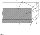
- the Figures 1 and 2 show schematic cross-sectional views through a composite material according to the invention. The cross-sectional areas are shown hatched.
- the composite material has an inner core layer 1 and two outer cover layers 2, 3.
- the inner core layer 1 consists of a palladium alloy with at least 30% by weight of palladium or of a platinum alloy with at least 30% by weight of platinum.
- Each of the two outer cover layers 2, 3 can consist of a precipitation-hardened and/or dispersion-hardened copper alloy with at least 90% by weight of copper or of a precipitation-hardened and/or dispersion-hardened silver alloy with at least 70% by weight of silver.
- the inner core layer 1 preferably consists of a palladium alloy as in the EP 3 960 890 A1 is described.
- the two outer cover layers 2, 3 preferably consist of a precipitation-hardened and/or dispersion-hardened copper alloy with at least 90% by weight of copper, particularly preferably of a precipitation-hardened copper alloy with at least 98% by weight of copper.
- the inner core layer 1 and the two outer cover layers 2, 3 can be firmly connected to one another and joined directly to one another by roll bonding strips of the respective material.
- the composite material has two opposing main surfaces 4, 5, which are formed by the outwardly facing surfaces of the cover layers 2, 3.
- the main surfaces 4, 5 can be arranged plane-parallel to one another.
- the composite material can form a flat cuboid, with the main surfaces 4, 5 preferably being larger than all other surfaces of the composite material combined.
- the inner core layer 1 and the two outer cover layers 2, 3 are joined together via interfaces 6, 7.
- the materials of the two outer cover layers 2, 3 and the inner core layer 1 can be mixed.
- a composite material according to the invention can be produced, for example, as follows: A sandwich made of three sheets with a precipitation-hardened and/or dispersion-hardened copper alloy and/or a precipitation-hardened and/or dispersion-hardened silver alloy at the top and bottom and a platinum alloy or a palladium alloy (in particular a palladium superlattice) in the middle is rolled together in a rolling pass with approx. 60-75% pass reduction, whereby these three sheets are cold welded and form a composite.
- the hardnesses of the materials are very similar, which is achieved by combining the precipitation-hardened and/or dispersion-hardened copper alloy and/or the precipitation-hardened and/or dispersion-hardened silver alloy in the hardened state with the palladium alloy or platinum alloy (in particular with a palladium superlattice alloy according to the EP 3 960 890 A1 ) is or will be rolled in the solution annealed state. After rolling to the desired thickness of 30-60 ⁇ m, the hardness and electrical conductivity of the platinum alloy or palladium alloy is adjusted by annealing at 380 ° C for 5 minutes (preferably under vacuum or under inert gas).
- the electrical conductivity and strength of the palladium alloy or platinum alloy increases significantly (see the palladium superlattice after EP 3 960 890 A1 ), without negatively affecting the mechanical and electrical properties of the copper alloy and/or silver alloy.
- the production of the palladium alloy can also be carried out analogously to that in EP 3 960 890 A1 described procedures.
- a sheet of a palladium alloy with the composition 36.5% by weight of copper, 10.5% by weight of silver, 1.5% by weight of ruthenium and the remainder palladium including less than 0.1% by weight of impurities was produced the EP 3 960 890 A1 and two sheets of precipitation-hardened copper alloy Wieland-K75 (C18070) rolled together with 0.3% by weight chromium, 0.1% by weight titanium, 0.02% by weight silicon and the rest copper. The composite was then rolled to a thickness of 54 ⁇ m.
- the in Figure 3 Composite material A shown therefore has an inner core layer 11 made of a palladium alloy with the composition 36.5% by weight of copper, 10.5% by weight of silver, 1.5% by weight of ruthenium and the balance of palladium including less than 0.1% by weight of impurities on.
- the core layer 11 is on both sides of two outer cover layers 12, 13 made of a precipitation-hardened copper alloy Wieland-K75 (C18070) with 0.3% by weight chromium, 0.1% by weight titanium, 0.02% by weight silicon and the rest Surrounded by copper.
- the two outer cover layers 12, 13 delimit the composite material A, each with a main surface 14, 15, which forms the largest part of the surface of the composite material A.
- the in Figure 4 Composite material B shown analogously has an inner core layer 21 made of a palladium alloy with the composition 36.5% by weight of copper, 10.5% by weight of silver, 1.5% by weight of ruthenium and the balance of palladium including less than 0.1% by weight of impurities on.
- the core layer 21 is on both sides of two outer cover layers 22, 23 made of a precipitation-hardened copper alloy Wieland-K75 (C18070) with 0.3% by weight chromium, 0.1% by weight titanium, 0.02% by weight silicon and the rest Surrounded by copper.
- the two outer cover layers 22, 23 delimit the composite material B, each with a main surface 24, 25, which forms the largest part of the surface of the composite material B.
- the inner core layer 21 and the two outer cover layers 22, 23 are joined together and firmly connected. There is no intermediate layer here either.
- the inner core layer 21 and the two outer cover layers 22, 23 are joined to one another via interfaces 26, 27. Mixing can occur in the area of the interfaces 26, 27 the materials of the two outer cover layers 22, 23 and the inner core layer 21 come.
- the electrical conductivity was then determined using a four-point measurement on one of the main surfaces 14, 15, 24, 25 of the composite materials A and B formed by the precipitation-hardened copper alloy.
- the four-point measurement method also known as four-point measurement or four-point measurement, is a method for determining the surface resistance, i.e. the electrical resistance of a surface or thin layer.
- four measuring tips are placed in a row on the surface of the main surface, with a known current flowing over the two outer measuring tips and the potential difference, that is, the electrical voltage between these two inner measuring tips, being measured with the two inner measuring tips. Since the method is based on the principle of four-wire measurement, it is largely independent of the contact resistance between the measuring tips and the surface (Thomson bridge principle). Adjacent measuring tips are each the same distance apart.
- the electrical conductivity results from the reciprocal of the specific resistance.
- a palladium-copper-silver alloy with the product name Hera 6321 with the composition 39% by weight of Pd, 31% by weight of Cu, 29% by weight of Ag, 0.9% by weight of Zn and 0.1% by weight of B was also examined .
- the measurements of the composite materials A and B were carried out on sheets with a thickness of 54 ⁇ m.
- the measurement of the Hera 6321 alloy was carried out on a sheet metal with a thickness of 54 ⁇ m.
- a strip made of a palladium alloy with at least 30% by weight of palladium and two strips of a precipitation-hardened and/or dispersion-hardened copper alloy with at least 90% by weight of copper can be provided or produced.
- the palladium alloy strip can be placed between the copper alloy strips.
- a third step 103 the strips can be joined together by roll cladding, the thickness of the strips being reduced during roll cladding.
- the thickness of the composite thus produced can be reduced to the target thickness (for example to 50 ⁇ m) by further rolling in one or more steps.
- the composite produced in this way can be annealed (for example at 380 ° C for 5 minutes) in order to set the desired hardness of the middle core layer 1 made of the palladium alloy.
- the composite material can be cut or punched into strips.
- test needles or bonding tapes can optionally be finalized.
- the core layers 1 of the strips can be worked out as tips of the test needles.
Abstract
Die Erfindung betrifft einen bandförmigen Sandwich-Verbundwerkstoff zur Herstellung von Prüfnadeln, wobei eine innere Kernschicht (1) zwischen zwei äußeren Deckschichten (2, 3) angeordnet ist, wobei die innere Kernschicht (1) aus einer Palladium-Legierung mit zumindest 30 Gew% Palladium oder aus einer Platin-Legierung mit zumindest 30 Gew% Platin besteht und wobei die zwei äußeren Deckschichten (2, 3) aus einer ausscheidungsgehärteten und/oder dispersionsgehärteten Kupfer-Legierung mit zumindest 90 Gew% Kupfer und/oder SilberLegierung mit zumindest 70 Gew% Silber bestehen.Die Erfindung betrifft auch eine Prüfnadel, ein Bondband, ein Prüfnadelarray sowie ein Verfahren zur Herstellung eines Verbundwerkstoffs.The invention relates to a strip-shaped sandwich composite material for producing test needles, an inner core layer (1) being arranged between two outer cover layers (2, 3), the inner core layer (1) being made of a palladium alloy with at least 30% by weight of palladium or consists of a platinum alloy with at least 30% by weight of platinum and wherein the two outer cover layers (2, 3) consist of a precipitation-hardened and/or dispersion-hardened copper alloy with at least 90% by weight of copper and/or a silver alloy with at least 70% by weight of silver The invention also relates to a test needle, a bonding tape, a test needle array and a method for producing a composite material.
Description
Die Erfindung betrifft einen bandförmigen, sandwichartig geschichteten Verbundwerkstoff, aus dem Prüfnadeln zur elektronischen Prüfung von Halbleiterelementen gestanzt oder geschnitten werden können sowie eine Prüfnadel, ein Bondband und ein Prüfnadelarray, das aus oder mit einem solchen bandförmigen, sandwichartig geschichteten Verbundwerkstoff hergestellt ist.The invention relates to a band-shaped, sandwich-like layered composite material from which test needles for electronic testing of semiconductor elements can be punched or cut, as well as a test needle, a bonding tape and a test needle array, which is made from or with such a band-shaped, sandwich-like layered composite material.
Die Erfindung betrifft auch ein Verfahren zur Herstellung eines solchen bandförmigen, sandwichartig geschichteten Verbundwerkstoffs aus zwei unterschiedlichen Materialien aus Bändern.The invention also relates to a method for producing such a band-shaped, sandwich-like layered composite material from two different materials from bands.
Aus dem Verbundwerkstoff können neben Prüfnadeln auch Bondbänder beziehungsweise Bonddrähte gefertigt werden, die von den gleichen physikalischen Eigenschaften profitieren, wie Prüfnadeln. Bondbänder sind bandförmige Bonddrähte.In addition to test needles, the composite material can also be used to make bonding tapes or bonding wires, which benefit from the same physical properties as test needles. Bonding tapes are tape-shaped bonding wires.
Während der Chipproduktion werden Wafer direkt nach der Prozessierung mit Prüfnadeln kontaktiert, um die Funktionsfähigkeit der von integrierten Schaltungen (IC) in ungesägtem Zustand zu testen. Ein Array von Prüfnadeln testet dabei nach der Strukturierung der einzelnen Chips den Halbleiterwafer auf Funktionalität. Die Prüfnadeln sind in einer Testkarte (probe card) fixiert, die auf das Design des Wafers abgestimmt ist. Beim Prüfprozess wird der Wafer auf die Prüfnadeln gepresst und eine Kontaktierung zwischen Prüfnadeln und den Pads der ICs hergestellt. Daraufhin werden verschiedene Parameter getestet, wie zum Beispiel die Kontaktierung, elektrische Kennwerte bei hoher Stromdichte und das elektrische Verhalten bei Temperaturwechseln.During chip production, wafers are contacted with test needles immediately after processing in order to test the functionality of the integrated circuits (IC) in the unsawed state. After structuring the individual chips, an array of test needles tests the functionality of the semiconductor wafer. The test needles are fixed in a test card (probe card) that is tailored to the design of the wafer. During the testing process, the wafer is pressed onto the test needles and contact is made between the test needles and the pads of the ICs. Various parameters are then tested, such as the contacting, electrical characteristics at high current densities and the electrical behavior during temperature changes.
Prüfnadeln werden also bei der Herstellung von Leistungselektronik, der Kontaktierung von Chips und anderen elektrischen Schaltungen zur Prüfung der Qualität von elektrischen Kontaktierungen eingesetzt (siehe hierzu beispielsweise die
Anwendungen wie Prüfnadeln oder Bondbänder in der Leistungselektronik erfordern neben einer hohen elektrischen Leitfähigkeit auch eine hohe mechanische Festigkeit und Härte. Zudem ist die Temperaturbeständigkeit beziehungsweise Warmfestigkeit von entscheidender Bedeutung.Applications such as test needles or bonding tapes in power electronics require not only high electrical conductivity but also high mechanical strength and hardness. In addition, temperature resistance or heat resistance is of crucial importance.
Die Schlüsselparamater einer guten Prüfnadel sind eine hohe elektrische Leitfähigkeit, da beim Prüfer der ICs für Leistungselektronik hohe elektrische Ströme übertragen werden müssen, sowie eine hohe Härte, um die Wartungsintervalle gering zu halten. Zudem profitieren Prüfnadeln und Bondbänder von einem geringem E-Modul (mE) und einer hohen Streckgrenze (Rp0,2), welche gute Federeigenschaften hervorrufen. Eine hohe thermische Leitfähigkeit bewirkt eine gute Abfuhr der Wärmeenergie und damit eine möglichst geringe zusätzliche thermische Erhöhung des elektrischen Widerstands. Geeignete Härte, E-Modul und Streckgrenze werden benötigt, um zum einen die Wartungsintervalle gering zu halten und zum anderen um gute Federeigenschaften der Prüfnadel zu realisieren.The key parameters of a good test needle are high electrical conductivity, since high electrical currents have to be transmitted when testing ICs for power electronics, as well as high hardness in order to keep maintenance intervals short. In addition, test needles and bonding tapes benefit from a low modulus of elasticity (m E ) and a high yield strength (Rp 0.2 ), which produce good spring properties. A high thermal conductivity ensures good dissipation of thermal energy and thus the lowest possible additional thermal increase in electrical resistance. Suitable hardness, modulus of elasticity and yield point are required in order to keep maintenance intervals short and to ensure good spring properties of the test needle.
Die elektrische Leitfähigkeit von reinem Kuper (100% IACS = 58,1 * 106 S/m) dient als Referenz zur Bestimmung der elektrischen Leitfähigkeit. Reines Kupfer (Cu) und reines Silber (Ag) können zu diesen Zwecken jedoch nicht eingesetzt werden, da sie deutlich zu duktil sind und sich die Prüfnadel beim Einsatz verformen würde.The electrical conductivity of pure copper (100% IACS = 58.1 * 10 6 S/m) serves as a reference for determining electrical conductivity. However, pure copper (Cu) and pure silver (Ag) cannot be used for these purposes because they are far too ductile and the test needle would deform when used.
Anwendungen wie Prüfnadeln ("Probe Needles") oder Bondbänder in der Leistungselektronik erfordern neben einer hohen elektrischen Leitfähigkeit auch eine hohe mechanische Festigkeit und Härte. Dabei ist auch die Temperaturbeständigkeit beziehungsweise die Warmfestigkeit von entscheidender Bedeutung.Applications such as probe needles or bonding tapes in power electronics require not only high electrical conductivity but also high mechanical strength and hardness. The temperature resistance or heat resistance is also of crucial importance.
Als Materialien für Prüfnadeln werden derzeit ausscheidungsgehärtete Kupfer-Legierungen, Rhodium-Legierungen (Rh-Legierungen) oder Palladium-Legierungen (Pd-Legierungen) verwendet, welche durch Kokillenguss, Lösungsglühen, Ausscheidungswärmebehandlung und Walzen zu dünnen Bändern mit einer Dicke von weniger als 55 µm verarbeitet werden.Precipitation-hardened copper alloys, rhodium alloys (Rh alloys) or palladium alloys (Pd alloys) are currently used as materials for test needles, which are formed into thin strips with a thickness of less than 55 µm by chill casting, solution annealing, precipitation heat treatment and rolling are processed.
Für die Anwendung auf Goldpads sind Palladium-Legierungen bekannt, wie beispielsweise Paliney® H3C der Firma Deringer Ney oder NewTec® der Firma Advanced Probing. Typische Materialien für Prüfnadeln sind ausscheidungsgehärtete Palladium-Silber-Legierungen, die 10 Gew% Gold und 10 Gew% Platin enthalten können und beispielsweise unter den Produktnamen Paliney® 7, Hera 6321 und Hera 648 vertrieben werden. Die
Für das Testen auf Aluminiumpads sind Prüfnadeln aus den Materialien Wolfram, Wolframcarbid, Palladium-Kupfer-Silber-Legierungen und Wolfram-Rhenium weit verbreitet. Diese sind besonders hart, wobei Aluminiumpads robuster als Goldpads sind und einer Prüfung mit harten Nadeln besser standhalten können als Goldpads. Diese Prüfnadeln haben auch keine sehr hohe elektrische Leitfähigkeit. Legierungen mit höherer elektrischer Leitfähigkeit wie CuAg7 sind weniger hart (ca. 320 HV1) und weniger warmfest als Palladium-Silber-Legierungen oder Palladium-Kupfer-Silber-Legierungen.Test needles made of tungsten, tungsten carbide, palladium-copper-silver alloys and tungsten-rhenium are widely used for testing on aluminum pads. These are particularly hard, with aluminum pads being more robust than gold pads and able to withstand testing with hard needles better than gold pads. These test needles also do not have a very high electrical conductivity. Alloys with higher electrical conductivity such as CuAg7 are less hard (approx. 320 HV1) and less heat-resistant than palladium-silver alloys or palladium-copper-silver alloys.
Weiterhin existieren PtNi30-Legierungen für Prüfnadeln im Markt. Aus der
Die
Bereits aus der
Als Materialien für Folien zur Herstellung von Prüfnadeln werden aber auch PtNi-Legierungen (Platin-Nickel-Legierungen) oder Rhodium (Rh) verwendet. Bei solchen Metallen oder Legierungen, die einen möglichst guten Kompromiss zwischen elektrischer Leitfähigkeit, thermischer Leitfähigkeit, Zugfestigkeit sowie Härte darstellen, beträgt die maximal mögliche elektrische Leitfähigkeit 5% bis 30% IACS und ist damit im Vergleich zu Kupfer eher gering.PtNi alloys (platinum-nickel alloys) or rhodium (Rh) are also used as materials for foils for the production of test needles. For metals or alloys that represent the best possible compromise between electrical conductivity, thermal conductivity, tensile strength and hardness, the maximum possible electrical conductivity is 5% to 30% IACS and is therefore rather low compared to copper.
Die
Die
Als Verbunddrähte zur Herstellung von Prüfnadeln oder Bonddrähten können beispielsweise rundumbeschichtete Drähte eingesetzt werden, die als sogenannte Manteldrähte oder Double-Drähte durch endlos Walzprozesse oder mit Hilfe von galvanischen Beschichtungen hergestellt werden können. Beispielsweise können diese im Inneren ein Unedel-Metall, beispielsweise aus einer Cu-Legierung wie CuBe2 aufweisen, ummantelt mit einer Edelmetall- Legierung (beispielsweise Hera238), um für kontakttechnische Anwendungen bei gleitenden Kontakten in Schleifringübertragern oder auch Schaltkontakten in Mikroschaltern eingesetzt werden zu können, so wie dies in der
Zur Verbesserung der elektrischen Leitfähigkeit der Prüfnadeln wird derzeit auch Rein-Kupfer galvanisch auf Palladium-Legierungen abgeschieden. Eine galvanische Beschichtung von Rhodium-Basislegierungen zur Herstellung eines Manteldrahts als Prüfnadel ist aus der
Nachteilig ist hieran, dass Rein-Kupfer nur eine geringe Härte, Warmfestigkeit und schlechte Federeigenschaften hat, wodurch die mechanischen Eigenschaften des so erzeugten Verbundwerkstoffs aus Palladium-Legierung und Kupfer negativ beeinflusst werden.The disadvantage of this is that pure copper has only low hardness, low temperature resistance and poor spring properties, which negatively influences the mechanical properties of the composite material produced in this way made of palladium alloy and copper.
Es wäre also wünschenswert, die galvanische beschichteten Palladium-Legierungen dahingehend zu verbessern, dass eine Verbesserung der elektrischen Leitfähigkeit ohne eine gleichzeitige Verschlechterung oder mit einer geringeren Verschlechterung der mechanischen Eigenschaften des Verbundwerkstoffs und der daraus hergestellten Prüfnadeln oder Bondbänder erzielt werden kann.It would therefore be desirable to improve the electroplated palladium alloys in such a way that an improvement in electrical conductivity can be achieved without a concomitant deterioration or with a lesser deterioration in the mechanical properties of the composite material and the test needles or bonding tapes made therefrom.
Die Aufgabe der Erfindung besteht also darin, die Nachteile des Stands der Technik zu überwinden. Insbesondere soll ein Verbundwerkstoff zur Herstellung von Prüfnadeln zur elektronischen Prüfung von Halbleiterelementen daraus (und zwar durch Stanzen oder Schneiden) sowie ein Verfahren zur Herstellung eines solchen Verbundwerkstoffs gefunden werden, bei dem der Verbundwerkstoff eine im Vergleich zu Palladium-Legierungen verbesserte elektrische Leitfähigkeit aufweist, ohne dass dabei die mechanischen Eigenschaften, insbesondere die Zugfestigkeit und die Warmzugfestigkeit und bevorzugt auch die Härte sich derart verschlechtert, wie das bei den galvanisch mit Rein-Kupfer beschichteten Palladium-Legierungen der Fall ist. Der Verbundwerkstoff und das Verfahren sollen einfach und kostengünstig zu realisieren sein und für die Massenproduktion tauglich sein. Aus dem Verbundwerkstoff sollen auf möglichst einfache und kostengünstige Weise Prüfnadeln und Bondbänder herstellbar sein, wobei die Spitze der Prüfnadel bevorzugt aus einer harten Palladium-Legierung oder Platin-Legierung bestehen soll. Ferner soll der Verbundwerkstoff eine möglichst mechanisch stabile Verbindung zwischen den Materialien des Verbundwerkstoffs aufweisen.The object of the invention is therefore to overcome the disadvantages of the prior art. In particular, a composite material for producing test needles for the electronic testing of semiconductor elements from it (by punching or cutting) and a method for producing such a composite material are to be found in which the composite material has improved electrical conductivity compared to palladium alloys, without the mechanical properties, in particular the tensile strength and the hot tensile strength and preferably also the hardness, deteriorating in the same way as those galvanically coated with pure copper Palladium alloys are the case. The composite material and the process should be simple and inexpensive to implement and suitable for mass production. Test needles and bonding tapes should be able to be produced from the composite material in the simplest and most cost-effective manner possible, with the tip of the test needle preferably consisting of a hard palladium alloy or platinum alloy. Furthermore, the composite material should have a connection that is as mechanically stable as possible between the materials of the composite material.
Die Aufgaben der Erfindung werden gelöst durch einen Verbundwerkstoff nach Anspruch 1, durch eine Prüfnadel oder ein Bondband nach Anspruch 9, durch ein Prüfnadelarray nach Anspruch 11, durch die Verwendung eines Verbunds, einer Prüfnadel oder eines Prüfnadelarrays nach Anspruch 12 sowie durch ein Verfahren nach Anspruch 13. Bevorzugte Ausführungen sind in den Unteransprüchen 2 bis 8, 10, 14 und 15 gezeigt.The objects of the invention are achieved by a composite material according to
Die Aufgaben der Erfindung werden gelöst durch einen Verbundwerkstoff zur Herstellung von Prüfnadeln zur elektronischen Prüfung von Halbleiterelementen, wobei der Verbundwerkstoff bandförmig ist und von zwei zueinander parallelen Hauptflächen begrenzt ist, wobei der Verbundwerkstoff senkrecht zu den parallelen Hauptflächen geschichtet ist und eine Sandwichbauweise mit einer inneren Kernschicht und zwei äußeren Deckschichten aufweist, wobei die innere Kernschicht zwischen den zwei äußeren Deckschichten angeordnet ist und die innere Kernschicht auf zwei gegenüberliegenden Seiten mit den zwei äußeren Deckschichten fest verbunden ist, wobei die zwei äußeren Deckschichten die parallelen Hauptflächen bilden, wobei die innere Kernschicht aus einer Palladium-Legierung mit zumindest 30 Gew% Palladium oder aus einer Platin-Legierung mit zumindest 30 Gew% Platin besteht und wobei die zwei äußeren Deckschichten aus einer ausscheidungsgehärteten und/oder dispersionsgehärteten Kupfer-Legierung mit zumindest 90 Gew% Kupfer oder aus einer ausscheidungsgehärteten und/oder dispersionsgehärteten Silber-Legierung mit zumindest 70 Gew% Silber oder aus einer ausscheidungsgehärteten und/oder dispersionsgehärteten Kupfer-Legierung mit zumindest 90 Gew% Kupfer und aus einer ausscheidungsgehärteten und/oder dispersionsgehärteten Silber-Legierung mit zumindest 70 Gew% Silber bestehen.The objects of the invention are achieved by a composite material for producing test needles for the electronic testing of semiconductor elements, the composite material being band-shaped and delimited by two mutually parallel main surfaces, the composite material being layered perpendicular to the parallel main surfaces and a sandwich construction with an inner core layer and has two outer cover layers, wherein the inner core layer is arranged between the two outer cover layers and the inner core layer is firmly connected to the two outer cover layers on two opposite sides, the two outer cover layers forming the parallel main surfaces, the inner core layer consisting of one Palladium alloy with at least 30% by weight of palladium or a platinum alloy with at least 30% by weight of platinum and the two outer cover layers made of a precipitation-hardened and / or dispersion-hardened copper alloy with at least 90% by weight of copper or of a precipitation-hardened and / or dispersion-hardened silver alloy with at least 70% by weight of silver or from a precipitation-hardened and/or dispersion-hardened copper alloy with at least 90% by weight of copper and from a precipitation-hardened and/or dispersion-hardened silver alloy with at least 70% by weight of silver.
Ausscheidungsgehärtete Kupfer-Legierungen und Silber-Legierungen bewirken eine hohe Härte und Zugfestigkeit.Precipitation-hardened copper alloys and silver alloys result in high hardness and tensile strength.
Dispersionsgehärtete Kupfer-Legierungen und Silber-Legierungen bewirken eine hohe Härte und Zugfestigkeit auch bei hohen Temperaturen.Dispersion-hardened copper alloys and silver alloys provide high hardness and tensile strength even at high temperatures.
Die ausscheidungsgehärtete und/oder dispersionsgehärtete Kupfer-Legierung und die ausscheidungsgehärtete und/oder dispersionsgehärtete Silber-Legierung können sowohl ausscheidungsgehärtet als auch dispersionsgehärtet sein.The precipitation hardened and/or dispersion hardened copper alloy and the precipitation hardened and/or dispersion hardened silver alloy can be both precipitation hardened and dispersion hardened.
Bei einer Ausscheidungshärtung einer Legierung entstehen durch eine Temperaturbehandlung Ausscheidungen in der Legierung. Bei einer Dispersionshärtung einer Legierung werden Dispersoide in der Legierung verteilt. Die Dispersoide können als Partikel in der Schmelze vor dem Erstarren verteilt sein. Solche Dispersoide sind häufig Oxide oder Boride, erfindungsgemäß bevorzugt Metall-Oxide.When an alloy is precipitation hardened, temperature treatment creates precipitates in the alloy. When an alloy is dispersion hardened, dispersoids are distributed throughout the alloy. The dispersoids can be distributed as particles in the melt before solidification. Such dispersoids are often oxides or borides, preferably metal oxides according to the invention.
Die parallelen Hauptflächen bilden die größte Oberfläche des bandförmigen Verbundwerkstoffs. Bevorzugt bilden die parallelen Hauptflächen zumindest 50% der Oberfläche des bandförmigen Verbundwerkstoffs, besonders bevorzugt bilden die parallelen Hauptflächen zumindest 90% der Oberfläche des bandförmigen Verbundwerkstoffs, ganz besonders bevorzugt bilden die parallelen Hauptflächen zumindest 99% der Oberfläche des bandförmigen Verbundwerkstoffs. Der bandförmige Verbundwerkstoff hat vorzugsweise in erster Näherung oder in guter Näherung die Form eines flachen Quaders.The parallel main surfaces form the largest surface area of the band-shaped composite material. The parallel main surfaces preferably form at least 50% of the surface of the band-shaped composite material, particularly preferably the parallel main surfaces form at least 90% of the surface of the band-shaped composite material, most preferably the parallel main surfaces form at least 99% of the surface of the band-shaped composite material. The band-shaped composite material preferably has the shape of a flat cuboid to a first approximation or to a good approximation.
Die zwei äußeren Deckschichten können aus unterschiedlichen Kupfer-Legierungen oder Silber-Legierungen bestehen. Es kann auch eine der zwei äußeren Deckschichten aus einer Kupfer-Legierung und die andere der zwei äußeren Deckschichten aus einer Silber-Legierung bestehen. Es wird jedoch erfindungsgemäß bevorzugt, dass die beiden äußeren Deckschichten aus der der gleichen Kupfer-Legierung oder Silber-Legierung bestehen, besonders bevorzugt aus der gleichen Kupfer-Legierung.The two outer cover layers can consist of different copper alloys or silver alloys. One of the two outer cover layers can also consist of a copper alloy and the other of the two outer cover layers can consist of a silver alloy. However, according to the invention, it is preferred that the two outer cover layers consist of the same copper alloy or silver alloy, particularly preferably the same copper alloy.
Die zueinander parallelen Hauptflächen müssen nicht im mathematischen Sinne vollkommen zueinander parallele oder planparallele Flächen bilden. Es reicht aus, wenn die zueinander parallelen Hauptflächen bis zu einem Winkel von maximal 5° gegeneinander geneigt sind. Bevorzugt sind die zueinander parallelen Hauptflächen mit einem Winkel von maximal 1° gegeneinander geneigt.The mutually parallel main surfaces do not have to form completely parallel or plane-parallel surfaces in the mathematical sense. It is sufficient if the main surfaces that are parallel to each other are inclined towards each other up to an angle of a maximum of 5°. The mutually parallel main surfaces are preferably inclined towards one another at an angle of a maximum of 1°.
Ebenfalls bevorzugt sind die zueinander parallelen Hauptflächen planparallel.The main surfaces that are parallel to one another are also preferably plane-parallel.
Bevorzugt sind die zueinander parallelen Hauptflächen ebene Flächen. Auch hier ist mit einer ebenen Fläche keine auf atomarem Bereich ebene Fläche gemeint, sondern eine ebene Fläche, wie sie beim Walzen entsteht.The main surfaces that are parallel to one another are preferably flat surfaces. Here, too, a flat surface does not mean a surface that is flat on an atomic level, but rather a flat surface such as that created during rolling.
Die Prüfnadeln und Bondbänder können aus dem bandförmigen Verbundwerkstoff hergestellt werden, indem Streifen des Verbundwerkstoffs senkrecht zu den parallelen Hauptflächen oder auch diagonal zu den parallelen Hauptflächen geschnitten werden. Zudem kann ein Ende der Nadel angespitzt werden und zwar bevorzugt in der Art, dass das Material der inneren Kernschicht eine Spitze der Prüfnadel bildet. Mit dieser Spitze kann dann eine Halbleiterstruktur hinsichtlich ihrer elektrischen Leitfähigkeit geprüft werden, indem die Spitze auf die zu untersuchende Halbleiteroberfläche gedrückt wird und die elektrische Leitfähigkeit über die Prüfnadel gemessen wird.The test needles and bonding tapes can be made from the tape-shaped composite material by cutting strips of the composite material perpendicular to the parallel main surfaces or diagonally to the parallel main surfaces. In addition, an end to the Needle are sharpened, preferably in such a way that the material of the inner core layer forms a tip of the test needle. This tip can then be used to test a semiconductor structure for its electrical conductivity by pressing the tip onto the semiconductor surface to be examined and measuring the electrical conductivity using the test needle.
Unter einer Verunreinigung ist vorliegend eine durch die Darstellung aller beteiligten Elemente bedingte Verunreinigung zu verstehen.In the present case, contamination is understood to mean contamination caused by the representation of all the elements involved.
Wenn das Material als Prüfnadel einsetzbar ist, dann ist es auch für den Einsatz als Bondband beziehungsweise Bonddraht geeignet.If the material can be used as a test needle, then it is also suitable for use as a bonding tape or bonding wire.
Bevorzugt sind die innere Kernschicht und die zwei äußeren Deckschichten metallisch. Ausscheidungsgehärtete und dispersionsgehärtete Kupfer-Legierungen und Silber-Legierungen bewirken eine hohe Härte und Zugfestigkeit des Verbundwerkstoffs auch bei hohen Temperaturen (etwa 300 °C).The inner core layer and the two outer cover layers are preferably metallic. Precipitation-hardened and dispersion-hardened copper alloys and silver alloys result in high hardness and tensile strength of the composite material even at high temperatures (around 300 °C).
Es kann bevorzugt vorgesehen sein, dass die innere Kernschicht mit den zwei äußeren Deckschichten gefügt ist, insbesondere durch walzplattieren gefügt ist.It can preferably be provided that the inner core layer is joined to the two outer cover layers, in particular joined by roll bonding.
Es kann vorgesehen sein, dass der bandförmige Verbundwerkstoff eine Stärke von maximal 300 µm hat, bevorzugt eine Stärke von maximal 100 µm hat.It can be provided that the band-shaped composite material has a thickness of a maximum of 300 μm, preferably a thickness of a maximum of 100 μm.
Die Stärke des Verbundwerkstoffs entspricht dem Abstand der beiden Hauptebenen, die von den äußeren Flächen der zwei äußeren Deckschichten gebildet werden.The thickness of the composite material corresponds to the distance between the two main planes formed by the outer surfaces of the two outer cover layers.
Dickere Verbundwerkstoffe sind ohne zusätzliches Walzen nicht ohne weiteres durch Schneiden oder Stanzen des Verbundwerkstoffs als Prüfnadeln einsetzbar.Thicker composite materials cannot easily be used as test needles by cutting or punching the composite material without additional rolling.
Ferner kann vorgesehen sein, dass die Dicke der inneren Kernschicht zumindest gleich dick ist wie die Dicke der beiden äußeren Deckschichten, bevorzugt zumindest doppelt so dick ist wie die Dicke der beiden äußeren Deckschichten.Furthermore, it can be provided that the thickness of the inner core layer is at least the same thickness as the thickness of the two outer cover layers, preferably at least twice as thick as the thickness of the two outer cover layers.
Auch kann vorgesehen sein, dass die Dicke der inneren Kernschicht maximal zehnmal so dick ist wie die Dicke der beiden äußeren Deckschichten, bevorzugt maximal fünfmal so dick ist wie die Dicke der beiden äußeren Deckschichten, besonders bevorzugt maximal dreimal so dick ist wie die Dicke der beiden äußeren Deckschichten.It can also be provided that the thickness of the inner core layer is a maximum of ten times as thick as the thickness of the two outer cover layers, preferably a maximum of five times as thick as the thickness of the two outer cover layers, particularly preferably a maximum of three times as thick as the thickness of the two outer covering layers.
Hierdurch wird sichergestellt, dass die physikalischen Eigenschaften des Verbunds von den Materialien der Deckschichten und der Kernschicht gemeinsam bestimmt werden.This ensures that the physical properties of the composite are jointly determined by the materials of the cover layers and the core layer.
Es kann vorgesehen sein, dass die innere Kernschicht unmittelbar mit den zwei äußeren Deckschichten verbunden ist.It can be provided that the inner core layer is connected directly to the two outer cover layers.
Das bedeutet, dass zwischen der inneren Kernschicht und den zwei äußeren Deckschichten keine weiteren Schichten, wie zum Beispiel eine Haftschicht und/oder eine Diffusionsschutzschicht angeordnet sind.This means that no further layers, such as an adhesive layer and/or a diffusion protection layer, are arranged between the inner core layer and the two outer cover layers.
Durch diese Maßnahme ist die Herstellung des Verbundwerkstoffs einfach und kostengünstig zu realisieren. Es hat sich gezeigt, dass bei der Herstellung des erfindungsgemäßen Verbundwerkstoffs mit einem erfindungsgemäßen Verfahren keine zusätzliche Zwischenschicht benötigt wird. Es kann beim Walzplattieren und bei einer nachfolgenden Wärmebehandlung eine Diffusionsschicht zwischen der inneren Kernschicht und den zwei äußeren Deckschichten entstehen. Diese wird nicht als eigene (weitere) Schicht im Sinne der vorliegenden Erfindung betrachtet, sondern als Verbindung im Bereich der Grenzfläche zwischen der inneren Kernschicht und den zwei äußeren Deckschichten.This measure makes it easy and cost-effective to produce the composite material. It has been shown that no additional intermediate layer is required when producing the composite material according to the invention using a method according to the invention. During roll cladding and subsequent heat treatment, a diffusion layer can arise between the inner core layer and the two outer cover layers. This is not viewed as a separate (additional) layer in the sense of the present invention, but rather as a connection in the area of the interface between the inner core layer and the two outer cover layers.
Des Weiteren kann vorgesehen sein, dass der Verbundwerkstoff aus der inneren Kernschicht und den äußeren Deckschichten besteht.Furthermore, it can be provided that the composite material consists of the inner core layer and the outer cover layers.
Hierdurch wird klargestellt, dass der Verbundwerkstoff keine weiteren Schichten oder Teile benötigt. Dadurch ist der Verbundwerkstoff kostengünstig in der Herstellung.This makes it clear that the composite material does not require any additional layers or parts. This makes the composite material cost-effective to produce.
Alternativ könnten beispielsweise die zwei äußeren Deckschichten an den Hauptflächen beschichtet sein oder es könnte an einer Kante des Verbundwerkstoffs ein Material zur elektrischen Kontaktierung der Prüfnadeln aufgetragen sein.Alternatively, for example, the two outer cover layers could be coated on the main surfaces or a material for electrical contacting of the test needles could be applied to one edge of the composite material.
Auch kann vorgesehen sein, dass die zwei äußeren Deckschichten aus einer ausscheidungsgehärteten und/oder dispersionsgehärteten Kupfer-Legierung mit zumindest 90 Gew% Kupfer bestehen, bevorzugt aus einer ausscheidungsgehärteten und/oder dispersionsgehärteten Kupfer-Legierung mit zumindest 97 Gew% Kupfer bestehen, besonders bevorzugt aus einer ausscheidungsgehärteten und/oder dispersionsgehärteten Kupfer-Legierung mit zumindest 99 Gew% Kupfer bestehen.It can also be provided that the two outer cover layers consist of a precipitation-hardened and/or dispersion-hardened copper alloy with at least 90% by weight of copper, preferably consist of a precipitation-hardened and/or dispersion-hardened copper alloy with at least 97% by weight of copper, particularly preferably a precipitation hardened and/or dispersion hardened copper alloy with at least 99% by weight of copper.
Ausscheidungsgehärtete und dispersionsgehärtete Kupfer-Legierungen mit hohem Kupferanteil sind besonders gut zur Herstellung von Prüfnadeln geeignet, da diese eine hohe elektrische Leitfähigkeit mit einer für Kupfer-Legierungen mit hohem Kupfer-Anteil relativ hohen Härte und Zugfestigkeit aufweisen.Precipitation-hardened and dispersion-hardened copper alloys with a high copper content are particularly suitable for the production of test needles because they have a high electrical conductivity with a hardness and tensile strength that are relatively high for copper alloys with a high copper content.
Bevorzugt kann auch vorgesehen sein, dass die innere Kernschicht aus einer Palladium-Legierung enthaltend zumindest 30 Gew% Palladium besteht, bevorzugt aus einer Palladium-Legierung enthaltend zumindest 35 Gew% Palladium besteht, besonders bevorzugt aus einer Palladium-Kupfer-Silber-Legierung nach der
Bevorzugt besteht die innere Kernschicht aus einer Palladium-Kupfer-Silber-Legierung enthaltend zumindest 35 Gew% Palladium, zumindest 20 Gew% Kupfer und zumindest 20The inner core layer preferably consists of a palladium-copper-silver alloy containing at least 35% by weight of palladium, at least 20% by weight of copper and at least 20% by weight
Gew% Silber, besonders bevorzugt aus einer Palladium-Kupfer-Silber-Legierung enthaltend 31 Gew% Kupfer und 29 Gew% Silber, bis zu 6 Gew% zumindest eines Elements, das ausgewählt ist aus der Gruppe, die aus Rhodium, Ruthenium und Rhenium besteht, und als Rest Palladium einschließlich Verunreinigungen besteht.% by weight of silver, particularly preferably from a palladium-copper-silver alloy containing 31% by weight of copper and 29% by weight of silver, up to 6% by weight of at least one element selected from the group consisting of rhodium, ruthenium and rhenium , and the remainder consists of palladium including impurities.
Besonders bevorzugt besteht die innere Kernschicht aus einer Palladium-Kupfer-Silber-Legierung nach der
Derartige Palladium-Legierungen bewirken eine besonders hohe Zugfestigkeit und Warmfestigkeit des Verbundwerkstoffs und der daraus hergestellten Prüfnadeln und Bondbänder.Such palladium alloys result in a particularly high tensile strength and high-temperature strength of the composite material and the test needles and bonding tapes made from it.
Es kann auch vorgesehen sein, dass der Verbundwerkstoff eine elektrische Leitfähigkeit gemessen mit einer Vierpunktmessmethode bei Raumtemperatur auf einer der zwei äußeren Deckschichten von zumindest 35% IACS (20,3 106 S/m) aufweist, bevorzugt von zumindest 40% IACS (23,2 106 S/m) aufweist, besonders bevorzugt von zumindest 45% IACS (26,1 106 S/m) aufweist.It can also be provided that the composite material has an electrical conductivity measured using a four-point measurement method at room temperature on one of the two outer cover layers of at least 35% IACS (20.3 10 6 S/m), preferably of at least 40% IACS (23, 2 106 S/m), particularly preferably of at least 45% IACS (26.1 10 6 S/m).
Des Weiteren kann vorgesehen sein, dass der Verbundwerkstoff eine Vickers-Härte HV0,05 bei Raumtemperatur in den zwei Deckschichten von zumindest 170 aufweist, bevorzugt von zumindest 190 aufweist, besonders bevorzugt von zumindest 196 aufweist.Furthermore, it can be provided that the composite material has a Vickers hardness HV0.05 at room temperature in the two cover layers of at least 170, preferably of at least 190, particularly preferably of at least 196.
Ferner kann vorgesehen sein, dass der Verbundwerkstoff eine Zugfestigkeit bei Raumtemperatur parallel zur Ebene der inneren Kernschicht von zumindest 1000 MPa aufweist, bevorzugt von zumindest 1100 MPa aufweist.Furthermore, it can be provided that the composite material has a tensile strength at room temperature parallel to the plane of the inner core layer of at least 1000 MPa, preferably of at least 1100 MPa.
Auch kann vorgesehen sein, dass der Verbundwerkstoff eine Streckgrenze bei Raumtemperatur parallel zur Ebene der inneren Kernschicht von zumindest 950 MPa aufweist, bevorzugt von zumindest 1050 MPa aufweist.It can also be provided that the composite material has a yield strength at room temperature parallel to the plane of the inner core layer of at least 950 MPa, preferably of at least 1050 MPa.
Diese physikalischen Eigenschaften des Verbundwerkstoffs können mit dem erfindungsgemäßen Verbundwerkstoff realisiert werden und bewirken vorteilhafte Materialeigenschaften für die daraus hergestellten Prüfnadeln und Bondbänder. Insbesondere bewirken die Kombinationen dieser physikalischen Eigenschaften sehr gute Eigenschaften für die Prüfnadeln und Bondbänder. Besonders die Kombination aus der hohen elektrischen Leitfähigkeit mit hoher Zugfestigkeit ist für Prüfnadeln und Bondbänder vorteilhaft.These physical properties of the composite material can be realized with the composite material according to the invention and bring about advantageous material properties for the test needles and bonding tapes made from it. In particular, the combinations of these physical properties result in very good properties for the test needles and bonding tapes. The combination of high electrical conductivity with high tensile strength is particularly advantageous for test needles and bonding tapes.
Die elektrische Leitfähigkeit kann mit einer 4-Pol Messung des Spannungsabfalls am Prüfling bei definierter Länge mit einem Burster Resistomat 2316 bestimmt werden. Die Messung erfolgt auf den Hauptflächen des Verbundwerkstoffs mit einer Fläche mit einer Kantenlänge von 5 mm oder mehr, einer Stärke von 55 µm und einem Messstrom von 10 mA.The electrical conductivity can be determined with a 4-pole measurement of the voltage drop on the test object at a defined length using a Burster Resistomat 2316. The measurement is carried out on the main surfaces of the composite material with a surface with an edge length of 5 mm or more, a thickness of 55 µm and a measuring current of 10 mA.
Ferner kann vorgesehen sein, dass der Verbundwerkstoff bei Raumtemperatur eine 0,2%-Dehngrenze Rp0,2 (Elastizitätsgrenze) von mindestens 1000 MPa aufweist, bevorzugt von mindestens 1150 MPa aufweist, besonders bevorzugt von 1300 MPa aufweist.Furthermore, it can be provided that the composite material has a 0.2% yield strength Rp 0.2 (elastic limit) of at least 1000 MPa at room temperature, preferably of at least 1150 MPa, particularly preferably of 1300 MPa.
Durch diese mechanischen und elektrischen Eigenschaften und insbesondere durch deren Kombination wird sichergestellt, dass der Verbundwerkstoff besonders gute elastische Eigenschaften und eine hohe elektrische Leitfähigkeit hat, um diesen als Prüfnadel oder Bondband einsetzen zu können.These mechanical and electrical properties and in particular their combination ensure that the composite material has particularly good elastic properties and high electrical conductivity in order to be able to use it as a test needle or bonding tape.
Die 0,2%-Dehngrenze Rp0,2 können mit einer Zwick Zugprüfmaschine Z250 bestimmt werden. Der Zugversuch kann an einem Verbundwerkstoff mit 50 µm Stärke und 13 mm Breite erfolgen und bezieht sich hierauf. Die Prüfgeschwindigkeit bezüglich der Streckgrenze Rp0,2 beträgt 1 mm/min.The 0.2% yield strength Rp 0.2 can be determined using a Zwick tensile testing machine Z250. The tensile test can be carried out on a composite material with a thickness of 50 µm and a width of 13 mm and refers to this. The test speed with regard to the yield strength Rp 0.2 is 1 mm/min.
Des Weiteren kann vorgesehen sein, dass die ausscheidungsgehärtete und/oder dispersionsgehärtete Kupfer-Legierung eine ausscheidungsgehärtete und/oder dispersionsgehärtete Kupfer-Chrom-Legierung mit zumindest 98 Gew% Kupfer ist, insbesondere eine ausscheidungsgehärtete und/oder dispersionsgehärtete CuCr1Zr-Legierung mit mindestens 0,5 Gew% und maximal 1,2 Gew% Chrom und mit mindestens 0,03 Gew% bis maximal 0,3 Gew% Zirkon und dem Rest Kupfer einschließlich Verunreinigungen ist.Furthermore, it can be provided that the precipitation-hardened and/or dispersion-hardened copper alloy is a precipitation-hardened and/or dispersion-hardened copper-chromium alloy with at least 98% by weight of copper, in particular a precipitation-hardened and/or dispersion-hardened CuCr1Zr alloy with at least 0.5 % by weight and a maximum of 1.2% by weight of chromium and with at least 0.03% by weight to a maximum of 0.3% by weight of zirconium and the rest is copper including impurities.
Auch kann vorgesehen sein, dass die ausscheidungsgehärtete und/oder dispersionsgehärtete Kupfer-Legierung eine ausscheidungsgehärtete Kupfer-Chrom-Titan-Legierung mit zumindest 99 Gew% Kupfer ist, insbesondere eine ausscheidungsgehärtete Kupfer-Chrom-Titan-Silizium-Legierung mit 0,3 Gew% Chrom, 0,1 Gew% Titan, 0,02 Gew% Si und dem Rest Kupfer einschließlich Verunreinigungen ist.It can also be provided that the precipitation-hardened and/or dispersion-hardened copper alloy is a precipitation-hardened copper-chromium-titanium alloy with at least 99% by weight of copper, in particular a precipitation-hardened copper-chromium-titanium-silicon alloy with 0.3% by weight. Chromium, 0.1% by weight titanium, 0.02% by weight Si and the balance is copper including impurities.
Ferner kann vorgesehen sein, dass die ausscheidungsgehärtete und/oder dispersionsgehärtete Kupfer-Legierung eine ausscheidungsgehärtete Kupfer-Chrom-Silber-Legierung mit zumindest 98 Gew% Kupfer ist, insbesondere eine ausscheidungsgehärtete Kupfer-Chrom-Silber-Eisen-Titan-Silizium-Legierung mit 0,5 Gew% Chrom, 0,2 Gew% Silber, 0,08 Gew% Eisen, 0,06 Gew% Titan, 0,03 Gew% Si und dem Rest Kupfer einschließlich Verunreinigungen ist.Furthermore, it can be provided that the precipitation-hardened and/or dispersion-hardened copper alloy is a precipitation-hardened copper-chromium-silver alloy with at least 98% by weight of copper, in particular a precipitation-hardened copper-chromium-silver-iron-titanium-silicon alloy with 0 .5% by weight of chromium, 0.2% by weight of silver, 0.08% by weight of iron, 0.06% by weight of titanium, 0.03% by weight of Si and the rest is copper including impurities.
Diese Kupfer-Legierungen werden erfindungsgemäß besonders bevorzugt.These copper alloys are particularly preferred according to the invention.
Des Weiteren kann vorgesehen sein, dass die ausscheidungsgehärtete und/oder dispersionsgehärtete Kupfer-Legierung eine ausscheidungsgehärtete und/oder dispersionsgehärtete Kupfer-Silber-Legierung mit zumindest 90 Gew% Kupfer ist, insbesondere eine ausscheidungsgehärtete und/oder dispersionsgehärtete Kupfer-Silber-Legierung mit mindestens 3 Gew% bis maximal 7 Gew% Silber und dem Rest Kupfer einschließlich Verunreinigungen oder dem Rest Kupfer einschließlich Verunreinigungen und einschließlich 0 Gew% bis maximal 2 Gew% oxidischen Dispersoiden ist.Furthermore, it can be provided that the precipitation-hardened and/or dispersion-hardened copper alloy is a precipitation-hardened and/or dispersion-hardened copper-silver alloy with at least 90% by weight of copper, in particular a precipitation-hardened and/or dispersion-hardened copper-silver alloy with at least 3 % by weight up to a maximum of 7% by weight of silver and the rest of copper including impurities or the rest of copper including impurities and including 0% by weight of up to a maximum of 2% by weight of oxidic dispersoids.
Eine solche Kupfer-Legierung mit 3 Gew% Silber (CuAg3) wird erfindungsgemäß besonders bevorzugt.Such a copper alloy with 3% by weight of silver (CuAg3) is particularly preferred according to the invention.
Ferner kann vorgesehen sein, dass die ausscheidungsgehärtete und/oder dispersionsgehärtete Silber-Legierung eine Silber-Kupfer-Legierung mit zumindest 70 Gew% Silber ist, bevorzugt eine Silber-Kupfer-Legierung mit mindestens 9 Gew% Kupfer und maximal 29 Gew% Kupfer und dem Rest Silber einschließlich Verunreinigungen ist, besonders bevorzugt eine Silber-Kupfer-Legierung mit 10 Gew% Kupfer und dem Rest Silber einschließlich Verunreinigungen ist oder eine Silber-Kupfer-Legierung mit 28 Gew% Kupfer und dem Rest Silber einschließlich Verunreinigungen ist.Furthermore, it can be provided that the precipitation-hardened and / or dispersion-hardened silver alloy is a silver-copper alloy with at least 70% by weight of silver, preferably a silver-copper alloy with at least 9% by weight of copper and a maximum of 29% by weight of copper and that The balance is silver including impurities, particularly preferably a silver-copper alloy with 10% by weight of copper and the remainder is silver including impurities or a silver-copper alloy with 28% by weight of copper and the remainder is silver including impurities.
Es kann auch vorgesehen sein, dass die Palladium-Legierung eine Palladium-Kupfer-Silber-Legierung mit Palladium als Hauptkomponente ist, wobei die Palladium-Kupfer-Silber-Legierung ein Gewichtsverhältnis von Palladium zu Kupfer von mindestens 1,05 und maximal 1,6 aufweist und ein Gewichtsverhältnis von Palladium zu Silber von mindestens 3 und maximal 6 aufweist und wobei die Palladium-Kupfer-Silber-Legierung mehr als 1 Gew% und bis maximal 6 Gew% Ruthenium, Rhodium oder Ruthenium und Rhodium und als Rest Palladium, Kupfer und Silber und maximal 1 Gew% andere metallische Elemente einschließlich Verunreinigungen enthält, bevorzugt weniger als 0,3 Gew% Iridium enthält.It can also be provided that the palladium alloy is a palladium-copper-silver alloy with palladium as the main component, the palladium-copper-silver alloy having a weight ratio of palladium to copper of at least 1.05 and a maximum of 1.6 and has a weight ratio of palladium to silver of at least 3 and a maximum of 6 and wherein the palladium-copper-silver alloy contains more than 1% by weight and up to a maximum of 6% by weight of ruthenium, rhodium or ruthenium and rhodium and the balance is palladium, copper and Silver and a maximum of 1% by weight of other metallic elements including impurities, preferably containing less than 0.3% by weight of iridium.
Diese Palladium-Kupfer-Silber-Legierung wird erfindungsgemäß besonders bevorzugt.This palladium-copper-silver alloy is particularly preferred according to the invention.
Ein Gewichtsverhältnis von Palladium zu Kupfer von mindestens 1,05 und maximal 1,6 bedeutet, dass das Palladium mit einem Gewicht von mindestens 105% und maximal 160% des Gewichts des in der Palladium-Kupfer-Silber-Legierung enthaltenen Kupfers in der Palladium-Kupfer-Silber-Legierung enthalten ist.A palladium to copper weight ratio of at least 1.05 and a maximum of 1.6 means that the palladium is present in the palladium with a weight of at least 105% and a maximum of 160% of the weight of the copper contained in the palladium-copper-silver alloy. Copper-silver alloy is included.
Dementsprechend bedeutet ein Gewichtsverhältnis von Palladium zu Silber von mindestens 3 und maximal 6, dass das Palladium mit einem Gewicht von mindestens dem dreifachen und maximal dem sechsfachen des Gewichts des in der Palladium-Kupfer-Silber-Legierung enthaltenen Silbers in der Palladium-Kupfer-Silber-Legierung enthalten ist.Accordingly, a weight ratio of palladium to silver of at least 3 and a maximum of 6 means that the palladium is present in the palladium-copper-silver with a weight of at least three times and a maximum of six times the weight of the silver contained in the palladium-copper-silver alloy -alloy is included.
Des Weiteren kann vorgesehen sein, dass die Palladium-Legierung eine Palladium-Silber-Kupfer-Platin-Legierung ist, insbesondere eine Palladium-Silber-Kupfer-Platin-Zink-Gold-Legierung mit 38 Gew% Silber, 15 Gew% Kupfer, 1,5 Gew% Platin, 1 Gew% Zink, 0,5 Gew% Gold und dem Rest Palladium einschließlich Verunreinigungen ist oder eine Palladium-Silber-Kupfer-Platin-Gold-Zink-Legierung mit 30 Gew% Silber, 14 Gew% Kupfer, 10 Gew% Platin, 10 Gew% Gold, 1 Gew% Zink und dem Rest Palladium einschließlich Verunreinigungen ist.Furthermore, it can be provided that the palladium alloy is a palladium-silver-copper-platinum alloy, in particular a palladium-silver-copper-platinum-zinc-gold alloy with 38% by weight of silver, 15% by weight of copper, 1 .5% by weight platinum, 1% by weight zinc, 0.5% by weight gold and the rest palladium including impurities or a palladium-silver-copper-platinum-gold-zinc alloy with 30% by weight silver, 14% by weight copper, 10% by weight platinum, 10% by weight gold, 1% by weight zinc and the rest palladium including impurities.
Auch kann vorgesehen sein, dass die Palladium-Legierung eine Palladium-Kupfer-Silber-Ruthenium-Legierung, insbesondere eine Palladium-Kupfer-Silber-Ruthenium-Legierung mit 36,5 Gew% Kupfer, 10,5 Gew% Silber, 1,5 Gew% Ruthenium und dem Rest Palladium einschließlich Verunreinigungen ist oder eine Palladium-Kupfer-Silber-Ruthenium-Rhenium-Legierung mit 36,5 Gew% Kupfer, 10,5 Gew% Silber, 1,1 Gew% Ruthenium, 0,4 Gew% Rhenium und dem Rest Palladium einschließlich Verunreinigungen ist.It can also be provided that the palladium alloy is a palladium-copper-silver-ruthenium alloy, in particular a palladium-copper-silver-ruthenium alloy with 36.5% by weight of copper, 10.5% by weight of silver, 1.5 Weight % ruthenium and the rest palladium including impurities or a palladium-copper-silver-ruthenium-rhenium alloy with 36.5% by weight copper, 10.5% by weight silver, 1.1% by weight ruthenium, 0.4% by weight rhenium and the rest palladium including impurities.
Des Weiteren kann vorgesehen sein, dass die Palladium-Legierung eine Palladium-Kupfer-Silber-Rhodium-Legierung ist, insbesondere eine Palladium-Kupfer-Silber-Rhodium-Legierung mit 36,5 Gew% Kupfer, 10,5 Gew% Silber, 1,5 Gew% Rhodium und dem Rest Palladium einschließlich Verunreinigungen ist.Furthermore, it can be provided that the palladium alloy is a palladium-copper-silver-rhodium alloy, in particular a palladium-copper-silver-rhodium alloy with 36.5% by weight of copper, 10.5% by weight of silver, 1 .5% by weight of rhodium and the rest is palladium including impurities.
Ferner kann vorgesehen sein, dass die Palladium-Legierung eine Palladium-Kupfer-Silber-Legierung ist, insbesondere eine Palladium-Kupfer-Silber-Legierung mit 31 Gew% Kupfer, 29 Gew% Silber und dem Rest Palladium einschließlich Verunreinigungen ist.Furthermore, it can be provided that the palladium alloy is a palladium-copper-silver alloy, in particular a palladium-copper-silver alloy with 31% by weight of copper, 29% by weight of silver and the rest is palladium including impurities.
Es kann des Weiteren vorgesehen sein, dass die Palladium-Legierung eine Palladium-Silber-Kupfer-Legierung ist, insbesondere eine Palladium-Silber-Kupfer-Legierung mit 38 Gew% Silber, 15 Gew% Kupfer und dem Rest Palladium einschließlich Verunreinigungen ist.It can further be provided that the palladium alloy is a palladium-silver-copper alloy, in particular a palladium-silver-copper alloy with 38% by weight of silver, 15% by weight of copper and the rest is palladium including impurities.
Auch kann vorgesehen sein, dass die Platin-Legierung eine Platin-Nickel-Legierung ist, bevorzugt eine Platin-Nickel-Legierung mit mindestens 3 Gew% und maximal 10 Gew% Nickel und dem Rest Platin einschließlich Verunreinigungen ist, besonders bevorzugt eine Platin-Nickel-Legierung mit 5 Gew% Nickel und dem Rest Platin einschließlich Verunreinigungen ist. Bei den vorgenannten Legierungen ist das Element mit dem höchsten Gewichtsanteil in der Legierung stets als erstes genannt. Bevorzugt ist das Element mit dem zweithöchsten Gewichtsanteil in der Legierung als zweites genannt. Besonders bevorzugt ist das Element mit dem dritthöchsten Gewichtsanteil in der Legierung als drittes genannt. Ganz besonders bevorzugt sind bei den genannten Legierungen die genannten Legierungsbestandteile in ihrer Reihenfolge nach ihrem Gewichtsanteil geordnet.It can also be provided that the platinum alloy is a platinum-nickel alloy, preferably a platinum-nickel alloy with at least 3% by weight and a maximum of 10% by weight of nickel and the rest is platinum including impurities, particularly preferably a platinum-nickel -Alloy with 5% nickel by weight and the rest platinum including impurities. In the aforementioned alloys, the element with the highest weight percentage in the alloy is always mentioned first. Preferably, the element with the second highest proportion by weight in the alloy is mentioned second. Particularly preferably, the element with the third highest proportion by weight in the alloy is named third. Very particularly preferably, in the alloys mentioned, the alloy components mentioned are arranged in their order according to their weight proportion.
Unter einer Hauptkomponente wird vorliegend das Element (in diesem Fall Palladium, Platin, Kupfer oder Silber) verstanden, das hauptsächlich, also mengenmäßig der größte Bestandteil ist, dass also beispielsweise mehr Palladium in einer Palladium-Kupfer-Silber-Legierung enthalten ist als Kupfer oder Silber.In the present case, a main component is understood to mean the element (in this case palladium, platinum, copper or silver) that is the main component, i.e. the largest component in terms of quantity, meaning that, for example, more palladium is contained in a palladium-copper-silver alloy than copper or Silver.
Diese Legierungen sind zur Herstellung des erfindungsgemäßen Verbundwerkstoffs besonders gut geeignet.These alloys are particularly suitable for producing the composite material according to the invention.
Es kann vorgesehen sein, dass die ausscheidungsgehärtete und/oder dispersionsgehärtete Kupfer-Legierung bis zu 2 Gew% Ausscheidungen und/oder Dispersoide aufweist oder aufweisen, bevorzugt bis zu 1 Gew% Ausscheidungen und/oder Dispersoide aufweist oder aufweisen, die Ausscheidungen und/oder Dispersoide zu zumindest 95 Gew% bestehend aus zumindest einem der Elemente ausgewählt aus der Liste, die aus Chrom, Titan, Silizium, Eisen, Sauerstoff, Zirkon und Silber besteht.It can be provided that the precipitation-hardened and/or dispersion-hardened copper alloy has or has up to 2% by weight of precipitates and/or dispersoids, preferably has or has up to 1% by weight of precipitates and/or dispersoids, the precipitates and/or dispersoids at least 95% by weight consisting of at least one of the elements selected from the list consisting of chromium, titanium, silicon, iron, oxygen, zirconium and silver.
Diese geringe Menge an Ausscheidungen und/oder Dispersoiden reicht aus, um die Härte der Kupfer-Legierung und gegebenenfalls auch der Silber-Legierung zu verbessern, ohne dass die elektrische Leitfähigkeit sehr stark reduziert würde.This small amount of precipitates and/or dispersoids is sufficient to improve the hardness of the copper alloy and possibly also the silver alloy without greatly reducing the electrical conductivity.
Der Anteil an Ausscheidungen und/oder Dispersoiden kann bestimmt werden, indem ein Querschliff der Kupfer-Legierung mittels Rasterelektronenmikroskopie oder auch Lichtmikroskopie hinsichtlich des Flächenverhältnisses von Ausscheidungen und/oder Dispersoiden zu der Gesamtfläche der Kupfer-Legierung ausgewertet wird, wobei hierzu die Dichte der Ausscheidungen und/oder Dispersoide und der sie umgebenden Matrix berücksichtigt werden muss. Die Dichte beispielsweise kann anhand einer Zusammensetzungsanalyse mittels Energiedispersiver oder Wellenlängendispersiver Röntgenanalyse (EDX oder WDX) oder mittels Röntgenfluoreszenz bestimmt werden.The proportion of precipitates and/or dispersoids can be determined by evaluating a cross-section of the copper alloy using scanning electron microscopy or light microscopy with regard to the area ratio of precipitates and/or dispersoids to the total area of the copper alloy, taking into account the density of the precipitates and /or dispersoids and the matrix surrounding them must be taken into account. The density, for example, can be determined using a composition analysis using energy-dispersive or wavelength-dispersive X-ray analysis (EDX or WDX) or using X-ray fluorescence.
Es kann vorgesehen sein, dass die ausscheidungsgehärtete und/oder dispersionsgehärtete Silber-Legierung bis zu 2 Gew% Ausscheidungen und/oder Dispersoide aufweist oder aufweisen, bevorzugt bis zu 1 Gew% Ausscheidungen und/oder Dispersoide aufweist oder aufweisen, die Ausscheidungen und/oder Dispersoide zu zumindest 95 Gew% bestehend aus zumindest einem der Elemente ausgewählt aus der Liste, die aus Chrom, Titan, Silizium, Eisen, Sauerstoff, Zirkon und Kupfer besteht.It can be provided that the precipitation-hardened and/or dispersion-hardened silver alloy has or has up to 2% by weight of precipitates and/or dispersoids, preferably has or has up to 1% by weight of precipitates and/or dispersoids, the precipitates and/or dispersoids at least 95% by weight consisting of at least one of the elements selected from the list consisting of chromium, titanium, silicon, iron, oxygen, zirconium and copper.
Ferner kann vorgesehen sein, dass die innere Kernschicht aus einer ausscheidungsgehärteten und/oder dispersionsgehärteten Palladium-Legierung oder aus einer ausscheidungsgehärteten und/oder dispersionsgehärteten Platin-Legierung besteht.Furthermore, it can be provided that the inner core layer consists of a precipitation-hardened and/or dispersion-hardened palladium alloy or of a precipitation-hardened and/or dispersion-hardened platinum alloy.
Hierdurch wird die Zugfestigkeit des Verbundwerkstoffs und die Standfestigkeit der Nadelspitze der daraus hergestellten Prüfnadeln verbessert. Bevorzugt besteht die innere Kernschicht aus einer ausscheidungsgehärteten und/oder dispersionsgehärteten Palladium-Legierung.This improves the tensile strength of the composite material and the stability of the needle tip of the test needles made from it. The inner core layer preferably consists of a precipitation-hardened and/or dispersion-hardened palladium alloy.
Die der vorliegenden Erfindung zugrundeliegenden Aufgaben werden auch gelöst durch eine Prüfnadel oder ein Bondband bestehend aus einem Streifen eines zuvor beschriebenen Verbundwerkstoffs.The tasks on which the present invention is based are also achieved by a test needle or a bonding tape consisting of a strip of a previously described composite material.
Die Prüfnadel und das Bondband profitieren von den vorteilhaften physikalischen Eigenschaften des Verbundwerkstoffs.The test needle and the bonding tape benefit from the advantageous physical properties of the composite material.
Dabei kann vorgesehen sein, dass die Prüfnadel eine Spitze aufweist, die aus dem Material der inneren Kernschicht besteht.It can be provided that the test needle has a tip which consists of the material of the inner core layer.
Hierdurch wird eine hohe Standfestigkeit der Prüfnadel erreicht. Die Prüfnadel mit dieser Spitze kann folglich sehr oft verwendet werden, ohne dass sie ausgetauscht oder sehr häufig aufbereitet werden muss.This ensures that the test needle has a high level of stability. The test needle with this tip can therefore be used very often without having to be replaced or reprocessed very frequently.
Die der vorliegenden Erfindung zugrundeliegenden Aufgaben werden ferner gelöst durch ein Prüfnadelarray aufweisend eine Mehrzahl von nebeneinander angeordneten vorgenannten Prüfnadeln.The tasks on which the present invention is based are further achieved by a test needle array having a plurality of the aforementioned test needles arranged next to one another.
Die der vorliegenden Erfindung zugrundeliegenden Aufgaben werden auch gelöst durch die Verwendung eines zuvor beschriebenen Verbundwerkstoffs oder einer zuvor beschriebenen Prüfnadel oder eines zuvor beschriebenen Prüfnadelarrays zum Prüfen von elektrischen Kontakten oder zur elektrischen Kontaktierung oder zur Herstellung eines Schleifkontakts.The objects on which the present invention is based are also achieved by using a previously described composite material or a previously described test needle or a previously described test needle array for testing electrical contacts or for electrical contacting or for producing a sliding contact.
Die der vorliegenden Erfindung zugrundeliegenden Aufgaben werden des Weiteren gelöst durch ein Verfahren zur Herstellung eines Verbundwerkstoffs aus zwei Metall-Legierungen, wobei der Verbundwerkstoff zur Herstellung von Prüfnadeln zur elektronischen Prüfung von Halbleiterelementen geeignet und vorgesehen ist und wobei das Verfahren durch die folgenden, chronologisch aufeinander folgenden Schritte gekennzeichnet ist:
- A) Bereitstellen eines ersten Bands aus einer Palladium-Legierung mit zumindest 30 Gew% Palladium oder aus einer Platin-Legierung mit zumindest 30 Gew% Platin und eines zweiten Bands aus einer ausscheidungsgehärteten und/oder dispersionsgehärteten Kupfer-Legierung mit zumindest 90 Gew% Kupfer oder aus einer ausscheidungsgehärteten und/oder dispersionsgehärteten Silber-Legierung mit zumindest 70 Gew% Silber und eines dritten Bands aus einer ausscheidungsgehärteten und/oder dispersionsgehärteten Kupfer-Legierung mit zumindest 90 Gew% Kupfer oder aus einer ausscheidungsgehärteten und/oder dispersionsgehärteten Silber-Legierung mit zumindest 70 Gew% Silber,
- B) Anordnen des ersten Bands zwischen das zweite Band und das dritte Band und Aneinanderlegen des ersten Bands an das zweite Band und an das dritte Band, und
- C) Verbinden des ersten Bands mit dem zweiten Band und dem dritten Band durch Walzplattieren der aneinander angelegten Bänder, wobei durch das Walzplattieren ein zusammenhängender bandförmiger Verbundwerkstoff aus den Materialien des ersten Bands, des zweiten Bands und der dritten Bands erzeugt wird.
- A) Providing a first strip made of a palladium alloy with at least 30% by weight of palladium or of a platinum alloy with at least 30% by weight of platinum and a second strip made of a precipitation-hardened and / or dispersion-hardened copper alloy with at least 90% by weight of copper or from a precipitation-hardened and/or dispersion-hardened silver alloy with at least 70% by weight of silver and a third strip made from a precipitation-hardened and/or dispersion-hardened copper alloy with at least 90% by weight of copper or from a precipitation-hardened and/or dispersion-hardened silver alloy with at least 70 wt% silver,
- B) placing the first band between the second band and the third band and abutting the first band on the second band and on the third band, and
- C) connecting the first band to the second band and the third band by roll bonding the bands placed against one another, the roll bonding producing a coherent band-shaped composite material from the materials of the first band, the second band and the third band.
Bevorzugt wird beim Walzplattieren die Dicke des ersten Bands, des zweiten Bands und des dritten Bands reduziert.During roll bonding, the thickness of the first band, the second band and the third band is preferably reduced.
Das Walzplattieren kann in mehreren Schritten durchgeführt werden, wobei die Dicke des Verbunds bei jedem Schritt reduziert wird.Roll cladding can be carried out in several steps, reducing the thickness of the composite at each step.
Bei erfindungsgemäßen Verfahren kann vorgesehen sein, dass nach Schritt C) ein Schritt D) erfolgt:
D) Temperaturbehandlung des in Schritt C) erzeugten Verbunds, wobei bei der Temperaturbehandlung das Material des ersten Bands ausscheidungsgehärtet und/oder dispersionsgehärtet wird.In the method according to the invention it can be provided that a step D) takes place after step C):
D) Temperature treatment of the composite produced in step C), wherein during the temperature treatment the material of the first strip is precipitation hardened and/or dispersion hardened.
Durch die nachgelagerte Temperaturbehandlung können die Bänder zuvor gut miteinander durch Walzen verbunden werden.Thanks to the subsequent temperature treatment, the strips can be well connected to each other by rolling.
Ferner kann vorgesehen sein, mit dem Verfahren ein zuvor beschriebener Verbundwerkstoff oder mit dem Verfahren durch Schneiden oder Stanzen des Verbundwerkstoffs zumindest eine zuvor beschriebene Prüfnadel oder zumindest ein zuvor beschriebenes Bondband hergestellt wird, bevorzugt mit dem Verfahren durch Schneiden oder Stanzen eine Vielzahl von zuvor beschriebenen Prüfnadeln oder Bondbändern hergestellt werden.Furthermore, it can be provided that with the method a previously described composite material or with the method by cutting or punching the composite material at least one previously described test needle or at least one previously described bonding tape is produced, preferably with the method by cutting or punching a plurality of previously described test needles or bond tapes.
Der Erfindung liegt die überraschende Erkenntnis zugrunde, dass eine Schicht aus einer festen und harten Palladium-Legierung oder Platin-Legierung auf beiden Seiten mit einer ausscheidungsgehärteten Kupfer-Legierung und/oder Silber-Legierung mit höherer elektrischer Leitfähigkeit beschichtet werden kann, um einen sandwichartige und bandförmigen Verbundwerkstoff zu erzeugen, dessen mechanische Eigenschaften im Vergleich zu einer mit Rein-Kupfer oder Rein-Silber beschichteten Palladium-Legierung oder Platin-Legierung bezüglich der Zugfestigkeit und Warmzugfestigkeit sowie der Härte verbessert sind, aber gleichzeitig eine deutliche Erhöhung der elektrischen Leitfähigkeit im Vergleich zu einer reinen harten Palladium-Legierung oder Platin-Legierung erreicht werden. Es wurde im Rahmen der vorliegenden Erfindung überraschend gefunden, dass sich eine derartige Beschichtung mit einer ausscheidungsgehärteten Kupfer-Legierung und/oder Silber-Legierung mit Hilfe von Walzplattier-Verfahren realisieren lässt, die mit einer galvanischen Beschichtung nicht zu fertigen wäre. Die vorliegende Erfindung beruht auch auf der Erkenntnis, dass sich die Kernschicht und die zwei äußeren Deckschichten bei ähnlicher Härte gut miteinander durch Walzplattieren fügen lassen.The invention is based on the surprising finding that a layer made of a solid and hard palladium alloy or platinum alloy can be coated on both sides with a precipitation-hardened copper alloy and / or silver alloy with higher electrical conductivity in order to create a sandwich-like and to produce a band-shaped composite material whose mechanical properties are improved compared to a palladium alloy or platinum alloy coated with pure copper or pure silver in terms of tensile strength and hot tensile strength as well as hardness, but at the same time a significant increase in electrical conductivity compared to a pure hard palladium alloy or platinum alloy can be achieved. In the context of the present invention, it was surprisingly found that such a coating with a precipitation-hardened copper alloy and/or silver alloy can be realized using roll cladding processes, which could not be produced with a galvanic coating. The present invention is also based on the knowledge that the core layer and the two outer cover layers can be easily joined to one another by roll bonding with similar hardness.
Der erfindungsgemäß bevorzugte Verbundwerkstoff aus einer Kupfer- und einer Palladium-Legierung für Leitungswerkstoffe oder Prüfnadeln kombiniert in vorteilhafter Weise die positiven Eigenschaften von Kupfer-Legierungen (hohe elektrische Leitfähigkeit) und Palladium-Legierungen (hohe Warmfestigkeit und gute Federeigenschaften). Damit erhält man einen Werkstoff der eine bessere Leitfähigkeit hat als die bestehenden Palladium-Legierungen (Hera 6321® oder Paliney H3C®) und eine bessere Warmfestigkeit und Gesamthärte als CuAg7. Die verwendeten Kupfer-Legierungen haben die vierfache Festigkeit von Rein-Kupfer bei ca. 80 % der elektrischen Leitfähigkeit von Rein-Kupfer und damit deutlich bessere Gesamteigenschaften. Diese beim Walzplattieren eingesetzten Legierungen können mit galvanischen Prozessen, die sich in der Regel auf Reinmetalle und wenige ausgewählte Legierungen beschränken, nicht abgeschieden werden.The preferred composite material according to the invention made of a copper and a palladium alloy for line materials or test needles advantageously combines the positive properties of copper alloys (high electrical conductivity) and palladium alloys (high heat resistance and good spring properties). This results in a material that has better conductivity than the existing palladium alloys (Hera 6321 ® or Paliney H3C ® ) and better high-temperature strength and overall hardness than CuAg7. The copper alloys used have four times the strength of pure copper with approx. 80% of the electrical conductivity of pure copper and therefore significantly better overall properties. These alloys used in roll cladding cannot be deposited using galvanic processes, which are usually limited to pure metals and a few selected alloys.
Galvanisch können auch mehrere verschiedene Schichten aus verschiedenen Metallen und Edelmetallen aufgebracht werden, um eine vorteilhafte Eigenschaftskombination zu erreichen.Several different layers made of different metals and precious metals can also be applied galvanically in order to achieve an advantageous combination of properties.
Allerdings können auf diese Weise keine ausscheidungshärtenden Legierungen abgeschieden werden und der Prozess wird auf diese Weise sehr aufwendig. Bei einer abschließenden Wärmebehandlung besteht zudem die Gefahr von Diffusion was sich aufgrund von Mischkristallbildung negativ auf die elektrische Leitfähigkeit auswirkt.However, no precipitation hardening alloys can be deposited in this way and the process becomes very complex. During a final heat treatment, there is also the risk of diffusion, which has a negative effect on the electrical conductivity due to the formation of mixed crystals.
Denkbar ist auch eine galvanisch mit Kupfer beschichtete Palladium-Legierung durch weiteres Walzen zu kaltverfestigen. Allerdings sind hier keine konsistenten Eigenschaften zu erwarten, da Kupfer- und Palladium-Legierungen deutlich verschiedene Härten aufweisen was eine ungleichmäßige Umformung zur Folge hat.It is also conceivable to work-harden a palladium alloy galvanically coated with copper by further rolling. However, consistent properties cannot be expected here, as copper and palladium alloys have significantly different hardnesses, which results in uneven forming.
Im Folgenden werden Ausführungsbeispiele der Erfindung anhand von vier schematisch dargestellten Figuren und einem Ablaufdiagramm erläutert, ohne jedoch dabei die Erfindung zu beschränken. Dabei zeigt:
-
Figur 1 : eine schematische Querschnittansicht durch einen Ausschnitt eines erfindungsgemäßen Verbundwerkstoffs; -
Figur 2 : eine schematische perspektivische Querschnittansicht durch einen Ausschnitt des erfindungsgemäßen Verbundwerkstoffs nachFigur 1 ; -
Figur 3 : eine lichtmikroskopische Aufnahme eines polierten Querschliffs eines erfindungsgemäßen Verbundwerkstoffs; -
Figur 4 : eine lichtmikroskopische Aufnahme eines polierten Querschliffs eines weiteren erfindungsgemäßen Verbundwerkstoffs; und -
Figur 5 : ein Ablaufdiagramm eines erfindungsgemäßen Verfahrens.
-
Figure 1 : a schematic cross-sectional view through a section of a composite material according to the invention; -
Figure 2 : a schematic perspective cross-sectional view through a section of the composite material according to the inventionFigure 1 ; -
Figure 3 : an optical micrograph of a polished cross section of a composite material according to the invention; -
Figure 4 : an optical micrograph of a polished cross section of another composite material according to the invention; and -
Figure 5 : a flowchart of a method according to the invention.
Die
Die innere Kernschicht 1 besteht aus einer Palladium-Legierung mit zumindest 30 Gew% Palladium oder aus einer Platin-Legierung mit zumindest 30 Gew% Platin. Jeder der zwei äußeren Deckschichten 2, 3 kann aus einer ausscheidungsgehärteten und/oder dispersionsgehärteten Kupfer-Legierung mit zumindest 90 Gew% Kupfer oder aus einer ausscheidungsgehärteten und/oder dispersionsgehärteten Silber-Legierung mit zumindest 70 Gew% Silber bestehen.The
Bevorzugt besteht die innere Kernschicht 1 aus einer Palladium-Legierung wie sie in der
Bevorzugt bestehen die zwei äußeren Deckschichten 2, 3 aus einer ausscheidungsgehärteten und/oder dispersionsgehärteten Kupfer-Legierung mit zumindest 90 Gew% Kupfer, besonders bevorzugt aus einer ausscheidungsgehärteten Kupfer-Legierung mit zumindest 98 Gew% Kupfer.The two
Die innere Kernschicht 1 und die zwei äußeren Deckschichten 2, 3 können durch Walzplattieren von Bändern des jeweiligen Materials fest miteinander verbunden und unmittelbar aneinander gefügt sein.The
Der Verbundwerkstoff weist zwei einander gegenüberliegende Hauptflächen 4, 5 auf, die durch die nach außen gerichteten Oberflächen der Deckschichten 2, 3 gebildet werden. Die Hauptflächen 4, 5 können planparallel zueinander angeordnet sein. Der Verbundwerkstoff kann in guter Näherung einen flachen Quader bilden, wobei die Hauptflächen 4, 5 vorzugsweise größer sind, als alle anderen Oberflächen des Verbundwerkstoffs zusammen.The composite material has two opposing
Die innere Kernschicht 1 und die zwei äußeren Deckschichten 2, 3 sind über Grenzflächen 6, 7 aneinander gefügt. Im Bereich der Grenzflächen 6, 7 kann es zu einer Durchmischung der Materialien der zwei äußeren Deckschichten 2, 3 und der inneren Kernschicht 1 kommen.The
Ein erfindungsgemäßer Verbundwerkstoff kann beispielsweise wie folgt hergestellt werden:
Ein Sandwich aus drei Blechen mit einer ausscheidungsgehärteten und/oder dispersionsgehärteten Kupfer-Legierung und/oder einer ausscheidungsgehärteten und/oder dispersionsgehärteten Silber-Legierung oben und unten sowie einer Platin-Legierung oder einer Palladium-Legierung (insbesondere einem Palladium-Superlattice) in der Mitte wird in einem Walzstich mit ca. 60-75 % Stichabnahme miteinander verwalzt, wobei diese drei Bleche kaltverschweißen und einen Verbund bilden. Die Härten der Werkstoffe sind dabei sehr ähnlich, was dadurch erreicht wird, dass die ausscheidungsgehärtete und/oder dispersionsgehärtete Kupfer-Legierung und/oder die ausscheidungsgehärtete und/oder dispersionsgehärtete Silber-Legierung im ausgehärteten Zustand mit der Palladium-Legierung oder Platin-Legierung (insbesondere mit einer Palladium-Superlattice-Legierung nach der
A sandwich made of three sheets with a precipitation-hardened and/or dispersion-hardened copper alloy and/or a precipitation-hardened and/or dispersion-hardened silver alloy at the top and bottom and a platinum alloy or a palladium alloy (in particular a palladium superlattice) in the middle is rolled together in a rolling pass with approx. 60-75% pass reduction, whereby these three sheets are cold welded and form a composite. The hardnesses of the materials are very similar, which is achieved by combining the precipitation-hardened and/or dispersion-hardened copper alloy and/or the precipitation-hardened and/or dispersion-hardened silver alloy in the hardened state with the palladium alloy or platinum alloy (in particular with a palladium superlattice alloy according to the
Zum Durchführen von Vergleichsmessungen wurden ein Blech einer Palladium-Legierung mit der Zusammensetzung 36,5 Gew% Kupfer, 10,5 Gew% Silber, 1,5 Gew% Ruthenium und dem Rest Palladium einschließlich weniger als 0,1 Gew% Verunreinigungen und hergestellt nach der
Zwei derartig hergestellte erfindungsgemäße Verbundwerkstoffe sind in den
Der in
Anschließend wurden die elektrische Leitfähigkeit mit einer Vierpunktmessung auf einer der durch die ausscheidungsgehärtete Kupfer-Legierung gebildeten Hauptflächen 14, 15, 24, 25 der Verbundwerkstoffe A und B bestimmt. Die Vierpunkt-Messmethode, auch Vierpunktmessung oder Vierspitzenmessung, ist ein Verfahren, um den Flächenwiderstand, also den elektrischen Widerstand einer Oberfläche oder dünnen Schicht, zu ermitteln. Bei dem Verfahren werden vier Messspitzen in einer Reihe auf die Oberfläche der Hauptfläche gebracht, wobei über die beiden äußeren Messspitzen ein bekannter Strom fließt und mit den beiden inneren Messspitzen der Potentialunterschied, das heißt, die elektrische Spannung zwischen diesen beiden inneren Messspitzen, gemessen wird. Da das Verfahren auf dem Prinzip der Vierleitermessung beruht, ist es weitgehend unabhängig vom Übergangswiderstand zwischen den Messspitzen und der Oberfläche (Prinzip Thomson-Brücke). Benachbarte Messspitzen haben jeweils den gleichen Abstand. Der Flächenwiderstand R ergibt sich aus der gemessenen Spannung U und dem Strom / nach der Formel: ![]()
![]()
Um aus dem Flächenwiderstand R den spezifischen Widerstand p des Schichtmaterials zu errechnen, multipliziert man ihn mit der Dicke d (Schichtdicke) der Folie: ![]()
![]()
Die elektrische Leitfähigkeit ergibt sich aus dem Kehrwert des spezifischen Widerstands.The electrical conductivity results from the reciprocal of the specific resistance.
Die Härte (HV0,05 - Vickers Härteprüfung nach DIN EN ISO 6507-1:2018 bis -4:2018 mit einer Prüfkraft von 0,4905 N (0,05 Kilopond)), die Festigkeit wurde mittels Zugversuchen untersucht. Die in den
Für den Vergleich wurde auch eine Palladium-Kupfer-Silber-Legierung mit dem Produktnamen Hera 6321 mit der Zusammensetzung 39 Gew% Pd, 31 Gew% Cu, 29 Gew% Ag, 0,9 Gew% Zn und 0,1 Gew% B untersucht.

Die Messungen der Verbundwerkstoffe A und B erfolgten an Blechen der Stärke 54 µm. Die Messung der Hera-6321-Legierung erfolgte an einem Blech der Stärke 54 µm.The measurements of the composite materials A and B were carried out on sheets with a thickness of 54 µm. The measurement of the Hera 6321 alloy was carried out on a sheet metal with a thickness of 54 µm.
Im Folgenden wird anhand von
In einem ersten Arbeitsschritt 101 können ein Band aus einer Palladium-Legierung mit zumindest 30 Gew% Palladium und zwei Bänder einer ausscheidungsgehärteten und/oder dispersionsgehärteten Kupfer-Legierung mit zumindest 90 Gew% Kupfer bereitgestellt oder hergestellt werden.In a first step 101, a strip made of a palladium alloy with at least 30% by weight of palladium and two strips of a precipitation-hardened and/or dispersion-hardened copper alloy with at least 90% by weight of copper can be provided or produced.
In einem zweiten Arbeitsschritt 102 kann das Band aus der Palladium-Legierung zwischen die Bänder aus der Kupfer-Legierung gelegt werden.In a second step 102, the palladium alloy strip can be placed between the copper alloy strips.
In einem dritten Arbeitsschritt 103 können die Bänder durch Walzplattieren miteinander gefügt werden, wobei die Stärke der Bänder beim Walzplattieren reduziert wird.In a third step 103, the strips can be joined together by roll cladding, the thickness of the strips being reduced during roll cladding.
In einem optionalen vierten Arbeitsschritt 104 kann die Stärke des so erzeugten Verbunds durch weiteres Walzen in einem oder in mehreren Schritten auf die Zielstärke (beispielsweise auf 50 µm) reduziert werden.In an optional fourth step 104, the thickness of the composite thus produced can be reduced to the target thickness (for example to 50 μm) by further rolling in one or more steps.
In einem fünften Arbeitsschritt 105 kann der so hergestellte Verbund ordnungsgeglüht werden (beispielsweise bei 380 °C für 5 Minuten), um die gewünschte Härte der mittleren Kernschicht 1 aus der Palladium-Legierung einzustellen.In a fifth step 105, the composite produced in this way can be annealed (for example at 380 ° C for 5 minutes) in order to set the desired hardness of the
In einem optionalen sechsten Arbeitsschritt 106 kann der Verbundwerkstoff in Streifen geschnitten oder gestanzt werden.In an optional
Anschließend kann optional in einem siebten Arbeitsschritt 107 eine Endfertigung von Prüfnadeln oder Bondbändern erfolgen. Hierzu können beispielsweise die Kernschichten 1 der Streifen als Spitzen der Prüfnadeln herausgearbeitet werden.Subsequently, in a seventh step 107, test needles or bonding tapes can optionally be finalized. For this purpose, for example, the core layers 1 of the strips can be worked out as tips of the test needles.
Die in der voranstehenden Beschreibung, sowie den Ansprüchen, Figuren und Ausführungsbeispielen offenbarten Merkmale der Erfindung können sowohl einzeln, als auch in jeder beliebigen Kombination für die Verwirklichung der Erfindung in ihren verschiedenen Ausführungsformen wesentlich sein.The features of the invention disclosed in the above description, as well as the claims, figures and exemplary embodiments can be essential for the implementation of the invention in its various embodiments both individually and in any combination.
- 1, 11, 211, 11, 21
- Innere KernschichtInner core layer
- 2, 12, 222, 12, 22
- Äußere DeckschichtOuter cover layer
- 3, 13, 233, 13, 23
- Äußere DeckschichtOuter cover layer
- 4, 14, 244, 14, 24
- Hauptflächemain area
- 5, 15, 255, 15, 25
- Hauptflächemain area
- 6, 16, 266, 16, 26
- Grenzflächeinterface
- 7, 17, 277, 17, 27
- Grenzflächeinterface
- 101101
- erster Arbeitsschrittfirst step of work
- 102102
- zweiter Arbeitsschrittsecond step
- 103103
- dritter Arbeitsschrittthird step
- 104104
- vierter Arbeitsschrittfourth step
- 105105
- fünfter Arbeitsschrittfifth step
- 106106
- sechster Arbeitsschrittsixth step
- 107107
- siebter Arbeitsschrittseventh step
Claims (15)
die zwei äußeren Deckschichten (2, 3, 12, 13, 22, 23) aus einer ausscheidungsgehärteten und/oder dispersionsgehärteten Kupfer-Legierung mit zumindest 90 Gew% Kupfer bestehen, bevorzugt aus einer ausscheidungsgehärteten und/oder dispersionsgehärteten Kupfer-Legierung mit zumindest 97 Gew% Kupfer bestehen, besonders bevorzugt aus einer ausscheidungsgehärteten und/oder dispersionsgehärteten Kupfer-Legierung mit zumindest 99 Gew% Kupfer bestehen.Composite material according to one of the preceding claims, characterized in that
the two outer cover layers (2, 3, 12, 13, 22, 23) consist of a precipitation-hardened and/or dispersion-hardened copper alloy with at least 90% by weight of copper, preferably of a precipitation-hardened and/or dispersion-hardened copper alloy with at least 97% by weight % copper, particularly preferably consisting of a precipitation-hardened and / or dispersion-hardened copper alloy with at least 99% by weight of copper.
die innere Kernschicht (1, 11, 21) aus einer Palladium-Legierung enthaltend zumindest 30 Gew% Palladium besteht, bevorzugt aus einer Palladium-Legierung enthaltend zumindest 35 Gew% Palladium besteht, besonders bevorzugt aus einer Palladium-Kupfer-Silber-Legierung nach der EP 3 960 890 A1.Composite material according to one of the preceding claims, characterized in that
the inner core layer (1, 11, 21) consists of a palladium alloy containing at least 30% by weight of palladium, preferably consists of a palladium alloy containing at least 35% by weight of palladium, particularly preferably of a palladium-copper-silver alloy according to EP 3 960 890 A1.
die ausscheidungsgehärtete und/oder dispersionsgehärtete Kupfer-Legierung bis zu 2 Gew% Ausscheidungen und/oder Dispersoide aufweist oder aufweisen, bevorzugt bis zu 1 Gew% Ausscheidungen und/oder Dispersoide aufweist oder aufweisen, die Ausscheidungen und/oder Dispersoide zu zumindest 95 Gew% bestehend aus zumindest einem der Elemente ausgewählt aus der Liste, die aus Chrom, Titan, Silizium, Eisen, Sauerstoff, Zirkon und Silber besteht.Composite material according to one of the preceding claims, characterized in that
the precipitation-hardened and/or dispersion-hardened copper alloy has or has up to 2% by weight of precipitates and/or dispersoids, preferably has or has up to 1% by weight of precipitates and/or dispersoids, the precipitates and/or dispersoids comprising at least 95% by weight at least one of the elements selected from the list consisting of chromium, titanium, silicon, iron, oxygen, zirconium and silver.
die innere Kernschicht (1, 11, 21) aus einer ausscheidungsgehärteten und/oder dispersionsgehärteten Palladium-Legierung oder aus einer ausscheidungsgehärteten und/oder dispersionsgehärteten Platin-Legierung besteht.Composite material according to one of the preceding claims, characterized in that
the inner core layer (1, 11, 21) consists of a precipitation-hardened and/or dispersion-hardened palladium alloy or of a precipitation-hardened and/or dispersion-hardened platinum alloy.
die Prüfnadel eine Spitze aufweist, die aus dem Material der inneren Kernschicht (1, 11, 21) besteht.Test needle according to claim 9, characterized in that
the test needle has a tip which consists of the material of the inner core layer (1, 11, 21).
nach Schritt C) ein Schritt D) erfolgt:
D) Temperaturbehandlung des in Schritt C) erzeugten Verbunds, wobei bei der Temperaturbehandlung das Material des ersten Bands ausscheidungsgehärtet und/oder dispersionsgehärtet wird.Method according to claim 13, characterized in that
after step C) a step D) takes place:
D) Temperature treatment of the composite produced in step C), wherein during the temperature treatment the material of the first strip is precipitation hardened and/or dispersion hardened.
mit dem Verfahren ein Verbundwerkstoff nach einem der Ansprüche 1 bis 8 oder mit dem Verfahren durch Schneiden oder Stanzen des Verbundwerkstoffs zumindest eine Prüfnadel oder zumindest ein Bondband nach einem der Ansprüche 9 oder 10 hergestellt wird, bevorzugt mit dem Verfahren durch Schneiden oder Stanzen eine Vielzahl von Prüfnadeln oder Bondbändern nach einem der Ansprüche 9 oder 10 hergestellt werden.Method according to claim 13 or 14, characterized in that
with the method a composite material according to one of claims 1 to 8 or with the method by cutting or punching the composite material at least one test needle or at least one bonding tape according to one of claims 9 or 10 is produced, preferably with the method by cutting or punching a plurality of Test needles or bonding tapes are produced according to one of claims 9 or 10.
Priority Applications (4)
| Application Number | Priority Date | Filing Date | Title |
|---|---|---|---|
| EP22190456.8A EP4325227A1 (en) | 2022-08-16 | 2022-08-16 | Tape-like composite material for test needles |
| JP2023114117A JP2024027093A (en) | 2022-08-16 | 2023-07-12 | Composite material in strip form for probe needles |
| KR1020230090771A KR20240024011A (en) | 2022-08-16 | 2023-07-13 | Strip-shaped composite material for probe needles |
| US18/447,683 US20240061016A1 (en) | 2022-08-16 | 2023-08-10 | Strip-shaped composite material for probe needles |
Applications Claiming Priority (1)
| Application Number | Priority Date | Filing Date | Title |
|---|---|---|---|
| EP22190456.8A EP4325227A1 (en) | 2022-08-16 | 2022-08-16 | Tape-like composite material for test needles |
Publications (1)
| Publication Number | Publication Date |
|---|---|
| EP4325227A1 true EP4325227A1 (en) | 2024-02-21 |
Family
ID=82940033
Family Applications (1)
| Application Number | Title | Priority Date | Filing Date |
|---|---|---|---|
| EP22190456.8A Pending EP4325227A1 (en) | 2022-08-16 | 2022-08-16 | Tape-like composite material for test needles |
Country Status (4)
| Country | Link |
|---|---|
| US (1) | US20240061016A1 (en) |
| EP (1) | EP4325227A1 (en) |
| JP (1) | JP2024027093A (en) |
| KR (1) | KR20240024011A (en) |
Citations (24)
| Publication number | Priority date | Publication date | Assignee | Title |
|---|---|---|---|---|
| GB354216A (en) | 1929-01-28 | 1931-07-28 | Int Nickel Co | Improvements in or relating to alloys of palladium, silver and copper |
| US5833774A (en) | 1997-04-10 | 1998-11-10 | The J. M. Ney Company | High strength silver palladium alloy |
| JP2006064511A (en) * | 2004-08-26 | 2006-03-09 | Sumitomo Electric Ind Ltd | Metallic structure |
| DE69635227T2 (en) * | 1995-05-26 | 2006-06-29 | Formfactor, Inc., Livermore | CONTACT SUPPORT FOR FITTING SUBSTRATES WITH SPRING CONTACTS |
| US20060197542A1 (en) | 2005-03-04 | 2006-09-07 | Tanaka Kikinzoku Kogyo K.K. | Material for probe pins |
| EP2060921A1 (en) | 2007-11-16 | 2009-05-20 | Technoprobe S.p.A | Contact probe for testing head having vertical probes and related testing head for testing microstructure electric performance |
| EP2139012A1 (en) * | 2007-03-27 | 2009-12-30 | The Furukawa Electric Co., Ltd. | Silver-coated material for movable contact component and method for manufacturing such silver-coated material |
| EP2159581A1 (en) * | 2007-06-06 | 2010-03-03 | Tanaka Kikinzoku Kogyo K.K. | Material for probe pin |
| US20100239453A1 (en) | 2008-02-27 | 2010-09-23 | Tomokazu Obata | Iridium alloy excellent in hardness, workability and anti-contamination properties |
| US20120286816A1 (en) | 2004-05-21 | 2012-11-15 | Microprobe, Inc. | Probes with high current carrying capability and laser machining methods |
| US20130099813A1 (en) | 2011-10-21 | 2013-04-25 | Tokyo Electron Limited | Contact terminal for a probe card, and the probe card |
| US20140176172A1 (en) | 2012-12-21 | 2014-06-26 | Kip Stevenson | Composite wire probe test assembly |
| US20140266278A1 (en) | 2013-03-18 | 2014-09-18 | Cheng Yun Technology Co., Ltd. | Probe needle |
| US20140377129A1 (en) | 2011-12-27 | 2014-12-25 | Tokuriki Honten Co., Ltd. | Palladium Alloy for Electric and Electronic Appliances |
| WO2016009293A1 (en) | 2014-07-14 | 2016-01-21 | Technoprobe S.P.A. | Contact probe for a testing head and corresponding manufacturing method |
| WO2016107729A1 (en) | 2014-12-30 | 2016-07-07 | Technoprobe S.P.A. | Contact probe for testing head |
| US20160252547A1 (en) | 2013-11-07 | 2016-09-01 | Heraeus Deutschland GmbH & Co. KG | Probe pin and method for producing a probe pin |
| US20190064215A1 (en) * | 2017-08-23 | 2019-02-28 | Leeno Industrial Inc. | Mems probe and test device using the same |
| US20190101569A1 (en) | 2017-09-29 | 2019-04-04 | Intel Corporation | Probes for wafer sorting |
| US10385424B2 (en) | 2016-01-29 | 2019-08-20 | Deringer-Ney, Inc. | Palladium-based alloys |
| DE102019130522A1 (en) | 2019-11-12 | 2021-05-12 | Heraeus Deutschland GmbH & Co. KG | Process for the production of composite wires |
| EP3878986A1 (en) * | 2020-03-12 | 2021-09-15 | Heraeus Deutschland GmbH & Co KG | Wire and ribbon with bornitride nanotubes for electrical contacts |
| EP3960890A1 (en) | 2020-09-01 | 2022-03-02 | Heraeus Deutschland GmbH & Co. KG | Palladium copper silver ruthenium alloy |
| EP3862759B1 (en) | 2020-02-04 | 2022-05-11 | Heraeus Deutschland GmbH & Co. KG | Sheathed wire and method for producing same |
-
2022
- 2022-08-16 EP EP22190456.8A patent/EP4325227A1/en active Pending
-
2023
- 2023-07-12 JP JP2023114117A patent/JP2024027093A/en active Pending
- 2023-07-13 KR KR1020230090771A patent/KR20240024011A/en unknown
- 2023-08-10 US US18/447,683 patent/US20240061016A1/en active Pending
Patent Citations (27)
| Publication number | Priority date | Publication date | Assignee | Title |
|---|---|---|---|---|
| GB354216A (en) | 1929-01-28 | 1931-07-28 | Int Nickel Co | Improvements in or relating to alloys of palladium, silver and copper |
| US1913423A (en) | 1929-01-28 | 1933-06-13 | Int Nickel Co | Precious metal alloy |
| DE69635227T2 (en) * | 1995-05-26 | 2006-06-29 | Formfactor, Inc., Livermore | CONTACT SUPPORT FOR FITTING SUBSTRATES WITH SPRING CONTACTS |
| US5833774A (en) | 1997-04-10 | 1998-11-10 | The J. M. Ney Company | High strength silver palladium alloy |
| US20120286816A1 (en) | 2004-05-21 | 2012-11-15 | Microprobe, Inc. | Probes with high current carrying capability and laser machining methods |
| JP2006064511A (en) * | 2004-08-26 | 2006-03-09 | Sumitomo Electric Ind Ltd | Metallic structure |
| US20060197542A1 (en) | 2005-03-04 | 2006-09-07 | Tanaka Kikinzoku Kogyo K.K. | Material for probe pins |
| EP2139012A1 (en) * | 2007-03-27 | 2009-12-30 | The Furukawa Electric Co., Ltd. | Silver-coated material for movable contact component and method for manufacturing such silver-coated material |
| EP2159581A1 (en) * | 2007-06-06 | 2010-03-03 | Tanaka Kikinzoku Kogyo K.K. | Material for probe pin |
| EP2060921A1 (en) | 2007-11-16 | 2009-05-20 | Technoprobe S.p.A | Contact probe for testing head having vertical probes and related testing head for testing microstructure electric performance |
| US20100239453A1 (en) | 2008-02-27 | 2010-09-23 | Tomokazu Obata | Iridium alloy excellent in hardness, workability and anti-contamination properties |
| EP2248920A1 (en) | 2008-02-27 | 2010-11-10 | Tanaka Kikinzoku Kogyo K.K. | Iridium alloy excellent in hardness, processability and stain proofness |
| US20130099813A1 (en) | 2011-10-21 | 2013-04-25 | Tokyo Electron Limited | Contact terminal for a probe card, and the probe card |
| US20140377129A1 (en) | 2011-12-27 | 2014-12-25 | Tokuriki Honten Co., Ltd. | Palladium Alloy for Electric and Electronic Appliances |
| US20140176172A1 (en) | 2012-12-21 | 2014-06-26 | Kip Stevenson | Composite wire probe test assembly |
| US20140266278A1 (en) | 2013-03-18 | 2014-09-18 | Cheng Yun Technology Co., Ltd. | Probe needle |
| US20160252547A1 (en) | 2013-11-07 | 2016-09-01 | Heraeus Deutschland GmbH & Co. KG | Probe pin and method for producing a probe pin |
| WO2016009293A1 (en) | 2014-07-14 | 2016-01-21 | Technoprobe S.P.A. | Contact probe for a testing head and corresponding manufacturing method |
| US20170307657A1 (en) | 2014-12-30 | 2017-10-26 | Technoprobe S.P.A. | Contact probe for testing head |
| WO2016107729A1 (en) | 2014-12-30 | 2016-07-07 | Technoprobe S.P.A. | Contact probe for testing head |
| US10385424B2 (en) | 2016-01-29 | 2019-08-20 | Deringer-Ney, Inc. | Palladium-based alloys |
| US20190064215A1 (en) * | 2017-08-23 | 2019-02-28 | Leeno Industrial Inc. | Mems probe and test device using the same |
| US20190101569A1 (en) | 2017-09-29 | 2019-04-04 | Intel Corporation | Probes for wafer sorting |
| DE102019130522A1 (en) | 2019-11-12 | 2021-05-12 | Heraeus Deutschland GmbH & Co. KG | Process for the production of composite wires |
| EP3862759B1 (en) | 2020-02-04 | 2022-05-11 | Heraeus Deutschland GmbH & Co. KG | Sheathed wire and method for producing same |
| EP3878986A1 (en) * | 2020-03-12 | 2021-09-15 | Heraeus Deutschland GmbH & Co KG | Wire and ribbon with bornitride nanotubes for electrical contacts |
| EP3960890A1 (en) | 2020-09-01 | 2022-03-02 | Heraeus Deutschland GmbH & Co. KG | Palladium copper silver ruthenium alloy |
Also Published As
| Publication number | Publication date |
|---|---|
| US20240061016A1 (en) | 2024-02-22 |
| JP2024027093A (en) | 2024-02-29 |
| KR20240024011A (en) | 2024-02-23 |
Similar Documents
| Publication | Publication Date | Title |
|---|---|---|
| DE3634495C2 (en) | Process for producing a copper-tin alloy and its use as a conductor material | |
| EP2193867B2 (en) | Method for manufacturing a wire electrode for electrical discharge cutting. | |
| EP2137330B1 (en) | Metal foil | |
| DE112010001811B4 (en) | Cu-Ni-Si-Mg alloy with improved conductivity and bendability | |
| DE60131763T2 (en) | MATERIALS FROM COPPER ALLOY FOR ELECTRONICS OR ELECTRONIC COMPONENTS | |
| DE10125586B4 (en) | Copper alloy for use in electrical and electronic parts | |
| EP3960890A1 (en) | Palladium copper silver ruthenium alloy | |
| DE102010012609A1 (en) | Sn-plated copper or Sn-plated copper alloy excellent in heat resistance and manufacturing method therefor | |
| DE112012006189T5 (en) | A cladded element, clad connector for a connector, a method of manufacturing a cladded element, and a method of making a clad connector for a connector | |
| DE10147968B4 (en) | Copper alloy of high mechanical strength | |
| DE3520407C2 (en) | Process for the thermomechanical treatment of copper-beryllium alloys containing cobalt | |
| EP3425665B1 (en) | Method for the production of a bonding wire | |
| EP2742161B1 (en) | Copper zinc alloy | |
| DE112017002557B4 (en) | Press-fit connection structure | |
| DE2924238C2 (en) | Electrical contact material and process for its manufacture | |
| DE112021002136T5 (en) | Alloy for a resistor and use of a resistor alloy in a resistor | |
| EP3529389B1 (en) | Copper-zinc alloy | |
| DE112005001271T5 (en) | Copper alloy for electrical and electronic devices | |
| EP3862759B1 (en) | Sheathed wire and method for producing same | |
| EP4325227A1 (en) | Tape-like composite material for test needles | |
| EP2662465B1 (en) | Rhodium alloy for manufacturing a wire for test needles | |
| WO2021180421A1 (en) | Wire and strip comprising boron nitride nanotubes for electrical contacts | |
| EP3680101B1 (en) | Layered cu/refractory metal film and method for producing the same | |
| DE102020003784A1 (en) | Electrical contact material, connector, connector, wiring harness and manufacturing method for an electrical contact material | |
| EP3680102A1 (en) | Layered ag/refractory metal film and method for producing the same |
Legal Events
| Date | Code | Title | Description |
|---|---|---|---|
| PUAI | Public reference made under article 153(3) epc to a published international application that has entered the european phase |
Free format text: ORIGINAL CODE: 0009012 |
|
| STAA | Information on the status of an ep patent application or granted ep patent |
Free format text: STATUS: REQUEST FOR EXAMINATION WAS MADE |
|
| 17P | Request for examination filed |
Effective date: 20220816 |
|
| AK | Designated contracting states |
Kind code of ref document: A1 Designated state(s): AL AT BE BG CH CY CZ DE DK EE ES FI FR GB GR HR HU IE IS IT LI LT LU LV MC MK MT NL NO PL PT RO RS SE SI SK SM TR |