EP4322229A2 - Method for manufacturing a uv-radiation detector device based on sic, and uv-radiation detector device based on sic - Google Patents
Method for manufacturing a uv-radiation detector device based on sic, and uv-radiation detector device based on sic Download PDFInfo
- Publication number
- EP4322229A2 EP4322229A2 EP23220528.6A EP23220528A EP4322229A2 EP 4322229 A2 EP4322229 A2 EP 4322229A2 EP 23220528 A EP23220528 A EP 23220528A EP 4322229 A2 EP4322229 A2 EP 4322229A2
- Authority
- EP
- European Patent Office
- Prior art keywords
- ohmic
- sic
- substrate
- carbon
- drift layer
- Prior art date
- Legal status (The legal status is an assumption and is not a legal conclusion. Google has not performed a legal analysis and makes no representation as to the accuracy of the status listed.)
- Pending
Links
Images



Classifications
-
- H—ELECTRICITY
- H10—SEMICONDUCTOR DEVICES; ELECTRIC SOLID-STATE DEVICES NOT OTHERWISE PROVIDED FOR
- H10D—INORGANIC ELECTRIC SEMICONDUCTOR DEVICES
- H10D64/00—Electrodes of devices having potential barriers
- H10D64/01—Manufacture or treatment
- H10D64/011—Manufacture or treatment of electrodes ohmically coupled to a semiconductor
- H10D64/0111—Manufacture or treatment of electrodes ohmically coupled to a semiconductor to Group IV semiconductors
- H10D64/0115—Manufacture or treatment of electrodes ohmically coupled to a semiconductor to Group IV semiconductors to silicon carbide
-
- H—ELECTRICITY
- H10—SEMICONDUCTOR DEVICES; ELECTRIC SOLID-STATE DEVICES NOT OTHERWISE PROVIDED FOR
- H10F—INORGANIC SEMICONDUCTOR DEVICES SENSITIVE TO INFRARED RADIATION, LIGHT, ELECTROMAGNETIC RADIATION OF SHORTER WAVELENGTH OR CORPUSCULAR RADIATION
- H10F30/00—Individual radiation-sensitive semiconductor devices in which radiation controls the flow of current through the devices, e.g. photodetectors
- H10F30/20—Individual radiation-sensitive semiconductor devices in which radiation controls the flow of current through the devices, e.g. photodetectors the devices having potential barriers, e.g. phototransistors
- H10F30/21—Individual radiation-sensitive semiconductor devices in which radiation controls the flow of current through the devices, e.g. photodetectors the devices having potential barriers, e.g. phototransistors the devices being sensitive to infrared, visible or ultraviolet radiation
- H10F30/289—Individual radiation-sensitive semiconductor devices in which radiation controls the flow of current through the devices, e.g. photodetectors the devices having potential barriers, e.g. phototransistors the devices being sensitive to infrared, visible or ultraviolet radiation the devices being transparent or semi-transparent devices
-
- H—ELECTRICITY
- H10—SEMICONDUCTOR DEVICES; ELECTRIC SOLID-STATE DEVICES NOT OTHERWISE PROVIDED FOR
- H10F—INORGANIC SEMICONDUCTOR DEVICES SENSITIVE TO INFRARED RADIATION, LIGHT, ELECTROMAGNETIC RADIATION OF SHORTER WAVELENGTH OR CORPUSCULAR RADIATION
- H10F30/00—Individual radiation-sensitive semiconductor devices in which radiation controls the flow of current through the devices, e.g. photodetectors
- H10F30/20—Individual radiation-sensitive semiconductor devices in which radiation controls the flow of current through the devices, e.g. photodetectors the devices having potential barriers, e.g. phototransistors
- H10F30/21—Individual radiation-sensitive semiconductor devices in which radiation controls the flow of current through the devices, e.g. photodetectors the devices having potential barriers, e.g. phototransistors the devices being sensitive to infrared, visible or ultraviolet radiation
-
- H—ELECTRICITY
- H10—SEMICONDUCTOR DEVICES; ELECTRIC SOLID-STATE DEVICES NOT OTHERWISE PROVIDED FOR
- H10F—INORGANIC SEMICONDUCTOR DEVICES SENSITIVE TO INFRARED RADIATION, LIGHT, ELECTROMAGNETIC RADIATION OF SHORTER WAVELENGTH OR CORPUSCULAR RADIATION
- H10F30/00—Individual radiation-sensitive semiconductor devices in which radiation controls the flow of current through the devices, e.g. photodetectors
- H10F30/20—Individual radiation-sensitive semiconductor devices in which radiation controls the flow of current through the devices, e.g. photodetectors the devices having potential barriers, e.g. phototransistors
- H10F30/21—Individual radiation-sensitive semiconductor devices in which radiation controls the flow of current through the devices, e.g. photodetectors the devices having potential barriers, e.g. phototransistors the devices being sensitive to infrared, visible or ultraviolet radiation
- H10F30/22—Individual radiation-sensitive semiconductor devices in which radiation controls the flow of current through the devices, e.g. photodetectors the devices having potential barriers, e.g. phototransistors the devices being sensitive to infrared, visible or ultraviolet radiation the devices having only one potential barrier, e.g. photodiodes
- H10F30/221—Individual radiation-sensitive semiconductor devices in which radiation controls the flow of current through the devices, e.g. photodetectors the devices having potential barriers, e.g. phototransistors the devices being sensitive to infrared, visible or ultraviolet radiation the devices having only one potential barrier, e.g. photodiodes the potential barrier being a PN homojunction
-
- H—ELECTRICITY
- H10—SEMICONDUCTOR DEVICES; ELECTRIC SOLID-STATE DEVICES NOT OTHERWISE PROVIDED FOR
- H10F—INORGANIC SEMICONDUCTOR DEVICES SENSITIVE TO INFRARED RADIATION, LIGHT, ELECTROMAGNETIC RADIATION OF SHORTER WAVELENGTH OR CORPUSCULAR RADIATION
- H10F30/00—Individual radiation-sensitive semiconductor devices in which radiation controls the flow of current through the devices, e.g. photodetectors
- H10F30/20—Individual radiation-sensitive semiconductor devices in which radiation controls the flow of current through the devices, e.g. photodetectors the devices having potential barriers, e.g. phototransistors
- H10F30/21—Individual radiation-sensitive semiconductor devices in which radiation controls the flow of current through the devices, e.g. photodetectors the devices having potential barriers, e.g. phototransistors the devices being sensitive to infrared, visible or ultraviolet radiation
- H10F30/22—Individual radiation-sensitive semiconductor devices in which radiation controls the flow of current through the devices, e.g. photodetectors the devices having potential barriers, e.g. phototransistors the devices being sensitive to infrared, visible or ultraviolet radiation the devices having only one potential barrier, e.g. photodiodes
- H10F30/223—Individual radiation-sensitive semiconductor devices in which radiation controls the flow of current through the devices, e.g. photodetectors the devices having potential barriers, e.g. phototransistors the devices being sensitive to infrared, visible or ultraviolet radiation the devices having only one potential barrier, e.g. photodiodes the potential barrier being a PIN barrier
-
- H—ELECTRICITY
- H10—SEMICONDUCTOR DEVICES; ELECTRIC SOLID-STATE DEVICES NOT OTHERWISE PROVIDED FOR
- H10F—INORGANIC SEMICONDUCTOR DEVICES SENSITIVE TO INFRARED RADIATION, LIGHT, ELECTROMAGNETIC RADIATION OF SHORTER WAVELENGTH OR CORPUSCULAR RADIATION
- H10F71/00—Manufacture or treatment of devices covered by this subclass
- H10F71/121—The active layers comprising only Group IV materials
-
- H—ELECTRICITY
- H10—SEMICONDUCTOR DEVICES; ELECTRIC SOLID-STATE DEVICES NOT OTHERWISE PROVIDED FOR
- H10F—INORGANIC SEMICONDUCTOR DEVICES SENSITIVE TO INFRARED RADIATION, LIGHT, ELECTROMAGNETIC RADIATION OF SHORTER WAVELENGTH OR CORPUSCULAR RADIATION
- H10F71/00—Manufacture or treatment of devices covered by this subclass
- H10F71/121—The active layers comprising only Group IV materials
- H10F71/1215—The active layers comprising only Group IV materials comprising at least two Group IV elements, e.g. SiGe
-
- H—ELECTRICITY
- H10—SEMICONDUCTOR DEVICES; ELECTRIC SOLID-STATE DEVICES NOT OTHERWISE PROVIDED FOR
- H10F—INORGANIC SEMICONDUCTOR DEVICES SENSITIVE TO INFRARED RADIATION, LIGHT, ELECTROMAGNETIC RADIATION OF SHORTER WAVELENGTH OR CORPUSCULAR RADIATION
- H10F71/00—Manufacture or treatment of devices covered by this subclass
- H10F71/128—Annealing
-
- H—ELECTRICITY
- H10—SEMICONDUCTOR DEVICES; ELECTRIC SOLID-STATE DEVICES NOT OTHERWISE PROVIDED FOR
- H10F—INORGANIC SEMICONDUCTOR DEVICES SENSITIVE TO INFRARED RADIATION, LIGHT, ELECTROMAGNETIC RADIATION OF SHORTER WAVELENGTH OR CORPUSCULAR RADIATION
- H10F71/00—Manufacture or treatment of devices covered by this subclass
- H10F71/138—Manufacture of transparent electrodes, e.g. transparent conductive oxides [TCO] or indium tin oxide [ITO] electrodes
-
- H—ELECTRICITY
- H10—SEMICONDUCTOR DEVICES; ELECTRIC SOLID-STATE DEVICES NOT OTHERWISE PROVIDED FOR
- H10F—INORGANIC SEMICONDUCTOR DEVICES SENSITIVE TO INFRARED RADIATION, LIGHT, ELECTROMAGNETIC RADIATION OF SHORTER WAVELENGTH OR CORPUSCULAR RADIATION
- H10F77/00—Constructional details of devices covered by this subclass
- H10F77/10—Semiconductor bodies
- H10F77/14—Shape of semiconductor bodies; Shapes, relative sizes or dispositions of semiconductor regions within semiconductor bodies
- H10F77/148—Shapes of potential barriers
-
- H—ELECTRICITY
- H10—SEMICONDUCTOR DEVICES; ELECTRIC SOLID-STATE DEVICES NOT OTHERWISE PROVIDED FOR
- H10F—INORGANIC SEMICONDUCTOR DEVICES SENSITIVE TO INFRARED RADIATION, LIGHT, ELECTROMAGNETIC RADIATION OF SHORTER WAVELENGTH OR CORPUSCULAR RADIATION
- H10F77/00—Constructional details of devices covered by this subclass
- H10F77/20—Electrodes
- H10F77/206—Electrodes for devices having potential barriers
-
- H—ELECTRICITY
- H10—SEMICONDUCTOR DEVICES; ELECTRIC SOLID-STATE DEVICES NOT OTHERWISE PROVIDED FOR
- H10F—INORGANIC SEMICONDUCTOR DEVICES SENSITIVE TO INFRARED RADIATION, LIGHT, ELECTROMAGNETIC RADIATION OF SHORTER WAVELENGTH OR CORPUSCULAR RADIATION
- H10F77/00—Constructional details of devices covered by this subclass
- H10F77/20—Electrodes
- H10F77/244—Electrodes made of transparent conductive layers, e.g. transparent conductive oxide [TCO] layers
-
- H—ELECTRICITY
- H10—SEMICONDUCTOR DEVICES; ELECTRIC SOLID-STATE DEVICES NOT OTHERWISE PROVIDED FOR
- H10F—INORGANIC SEMICONDUCTOR DEVICES SENSITIVE TO INFRARED RADIATION, LIGHT, ELECTROMAGNETIC RADIATION OF SHORTER WAVELENGTH OR CORPUSCULAR RADIATION
- H10F77/00—Constructional details of devices covered by this subclass
- H10F77/30—Coatings
- H10F77/306—Coatings for devices having potential barriers
-
- Y—GENERAL TAGGING OF NEW TECHNOLOGICAL DEVELOPMENTS; GENERAL TAGGING OF CROSS-SECTIONAL TECHNOLOGIES SPANNING OVER SEVERAL SECTIONS OF THE IPC; TECHNICAL SUBJECTS COVERED BY FORMER USPC CROSS-REFERENCE ART COLLECTIONS [XRACs] AND DIGESTS
- Y02—TECHNOLOGIES OR APPLICATIONS FOR MITIGATION OR ADAPTATION AGAINST CLIMATE CHANGE
- Y02P—CLIMATE CHANGE MITIGATION TECHNOLOGIES IN THE PRODUCTION OR PROCESSING OF GOODS
- Y02P70/00—Climate change mitigation technologies in the production process for final industrial or consumer products
- Y02P70/50—Manufacturing or production processes characterised by the final manufactured product
Definitions
- the present invention relates to a method for manufacturing a UV-radiation detector device and to a UV-radiation detector device.
- the present invention relates to a photodetector diode with anode terminal and/or cathode terminal that are transparent to the UV radiation to be detected.
- semiconductor materials that have a wide bandgap, in particular, an energy value Eg of the bandgap higher than 1.1 eV, low on-state resistance (R ON ), a high value of thermal conductivity, high operating frequency and high speed of saturation of the charge carriers are ideal for producing electronic components, such as diodes or transistors, in particular for power applications.
- a material having these characteristics, and designed for being used for manufacturing electronic components is silicon carbide (SiC).
- SiC silicon carbide
- silicon carbide in its different polytypes (for example, 3C-SiC, 4H-SiC, 6H-SiC), is preferable to silicon as regards the properties listed previously.
- Electronic devices provided on a silicon-carbide substrate as compared to similar devices provided on a silicon substrate, present numerous advantages, such as low output on-state resistance, low leakage current, high operating temperature and high operating frequencies.
- detection of ultraviolet (UV) radiation for example coming from the Sun, from astronomic objects, or from artificial sources (in the medical, military, environmental, and astronomical fields) has received a considerable attention in the last few years.
- the manufacture of arrays of high-sensitivity diodes therefore present particular interest.
- wide-band-gap materials are excellent candidates for the detection of UV radiation; silicon carbide is consequently particularly suited for the purpose.
- SiC polytypes 4H-SiC is preferable for detecting UV radiation, thanks to its wide band gap (approximately 3.3 eV).
- Schottky or PN photodiodes of a known type, for detection of UV radiation are manufactured on a 4H-SiC epitaxial layer grown on a heavily doped substrate.
- Schottky contacts are provided on the front of the photodiode by formation of metal regions that provide the Schottky contacts, while an ohmic contact is provided on the back of the photodiode, for example by formation of a nickel layer followed by a fast thermal annealing (at approximately 950-1000°C).
- the Schottky contacts on the front side are obtained by defining, by lithographic processes, structures of titanium or nickel-silicide that are typically combfingered.
- the geometry of Schottky contacts on the front side (front electrode) is chosen so as to enable direct exposure to the radiation to be detected and vertical-conduction electrical operation of the Schottky photodiode thus manufactured.
- the area of the single diode directly exposed to UV radiation and electro-optically active is limited by the presence of the front Schottky contacts, which reflect and/or absorb the UV radiation and therefore reduce the useful area effectively exposed.
- Figure 1 shows, in side cross-sectional view in a (triaxial) cartesian reference system of axes X, Y, Z, a vertical-conduction Schottky diode 1 of a known type.
- the Schottky diode 1 includes: a substrate 3 of heavily doped SiC of a N type (e.g., 1 ⁇ 10 20 atoms/cm 3 ), provided with a surface 3a opposite to a surface 3b; a drift layer 2 of SiC grown epitaxially on the surface 3a of the substrate 3, having a dopant concentration of an N type lower than the dopant concentration of the substrate 3; an ohmic-contact region 6 (for example of nickel silicide), which extends over the surface 3b of the substrate 3; a cathode metallization 16, which extends over the ohmic-contact region 6; and an anode metallization 8, which extends over a top surface 2a of the drift layer 2.
- a substrate 3 of heavily doped SiC of a N type e.g., 1 ⁇ 10 20 atoms/cm 3
- drift layer 2 of SiC grown epitaxially on the surface 3a of the substrate 3, having a dopant concentration of an N type lower than the
- Schottky contacts or junctions are consequently formed at the interface between the drift layer 2 and the anode metallization 8.
- Schottky junctions are formed by portions of the drift layer 2 in direct electrical contact with respective portions of the anode metallization 8.
- a disadvantage of this device is the reduction of the active area, i.e., of the area dedicated to generation of charge carriers following upon interaction with the UV radiation to be detected.
- the portions of the surface 2a coated by the anode metallization 8 do not participate in the detection of the UV radiation and subsequent generation of the charge carriers on account of absorption and/or reflection of the UV radiation itself to be detected by the anode metallization 8.
- the aim of the present invention is to provide a method for manufacturing a UV-radiation detector device, as well as a UV-radiation detector device that will be able to overcome the drawbacks of the prior art.
- a method for manufacturing a UV-radiation detector device and a UV-radiation detector device are provided as defined in the annexed claims.
- Figure 2 shows, in side cross-sectional view in a (triaxial) cartesian reference system of axes X, Y, Z, a device 50, in particular a device for detecting ultraviolet radiation (UV), in particular a PN diode, according to one aspect of the present invention.
- the device 50 is designed to detect radiation having a wavelength in the 200-nm to 380-nm range.
- the device 50 includes: a substrate 53, of SiC of an N type, having a first dopant concentration, provided with a surface 53a opposite to a surface 53b, and having a thickness comprised between 50 ⁇ m and 350 ⁇ m, for example equal to 180 ⁇ m; a drift layer (e.g., grown epitaxially) 52, of SiC of an N type, having a second dopant concentration lower than the first dopant concentration, which extends over the surface 53a of the substrate 53 and has a thickness comprised, for example, between 5 and 100 ⁇ m; an ohmic-contact region or layer 56 (for example, of nickel silicide), which extends over the surface 53b of the substrate 53; a cathode metallization 57, for example of Ti/NiV/Ag or Ti/NiV/Au, which extends over the ohmic-contact region 56; an implanted anode region 59, which extends in the drift layer 52, facing the top surface 52a of the drift layer
- the doping level of the substrate 53 is, for example, comprised between 1 ⁇ 10 19 and 1 ⁇ 10 22 atoms/cm 3 ; the doping level of the drift layer 52 is, for example, comprised between 1 ⁇ 10 13 and 5 ⁇ 10 16 atoms/cm 3 ; the doping level of the implanted anode region 59 is, for example, equal to or higher than to 1 ⁇ 10 18 atoms/cm 3 .
- the ohmic-contact layer 60 includes one or more carbon-rich layers, which comprise, for example, graphite layers, or graphene multi-layers. More in particular, the ohmic-contact layer 60 has, on the surface 52a, an Si/C amorphous layer in which the carbon atoms are preponderant (for example, at least twice as many, in particular from twice to 100 times as many) as compared to the silicon atoms, following upon a separation of phase between the silicon atoms and the carbon atoms of the SiC substrate.
- preponderant for example, at least twice as many, in particular from twice to 100 times as many
- said one or more carbon-rich layers can be identified with the following chemical formula: Si (1-x) C x wherein x is comprised between 0.8 and 1 (in particular 0.8 ⁇ x ⁇ 1).
- the ohmic-contact layer 60 may present a layer including carbon clusters (e.g., graphite layer), having a thickness greater than that of the amorphous layer. Formation of this ohmic-contact layer 60 is due to a thermal decomposition of silicon carbide, as a result of the manufacturing process illustrated in what follows.
- the ohmic-contact layer 60 is self-aligned, on the surface 52a, with the implanted region 59 (i.e., in top view in the plane XY, the ohmic-contact layer 60 has the same shape and extension as the implanted region 59).
- the ohmic-contact layer 60 does not extend, along Z, beyond the surface 52a; in other words, the ohmic-contact layer 60 has a top surface 60a coplanar (i.e., aligned along X) with the surface 52a, and extends in depth (along Z) in the implanted region 59 for a depth comprised between one nanometre and some tens of nanometres (e.g., between 1 and 20 nm) measured starting from the surface 52a.
- the shape in plan view, or "layout”, of the implanted region 59 (and therefore of the ohmic-contact layer 60) in the plane XY can be chosen according to the need, in the design stage.
- the implanted region 59 can extend continuously (in top view in the plane XY) over the entire active area of the device 50, or else only over a portion of the active area of the device 50, or else may be formed by a plurality of implanted sub-regions separated from one another by portions of the drift layer 52.
- an ohmic-contact layer 60 of the type described previously is transparent to UV radiation, in particular to radiation with a wavelength in the 200-nm to 380-nm range. Therefore, in use, even in the case where the ohmic-contact layer 60 were to cover the entire active area of the device 50, the UV radiation to be detected would traverse in any case the ohmic-contact layer 60, reaching the drift layer 52 and generating, in a per se known manner, the charge carriers.
- By appropriately polarizing the device 50 between the anode and the cathode e.g., by bonding wires) it is thus possible to collect and measure a current induced by the UV radiation, in a way in itself known that does not form part of the present invention.
- Steps of formation of the device 50 are described in what follows, only with reference to the steps of formation of the ohmic-contact layer 60 (the remaining steps are carried out according to the prior art).
- a wafer 100 is arranged, including the substrate 53 of SiC (in particular, 4H-SiC; however, other polytypes may be used such as, though not exclusively, 2H-SiC, 3C-SiC and 6H-SiC).
- SiC in particular, 4H-SiC; however, other polytypes may be used such as, though not exclusively, 2H-SiC, 3C-SiC and 6H-SiC).
- the substrate 53 has a first conductivity type (in this embodiment a doping of an N type) and is provided with the front surface 53a and the back surface 53b, which are opposite to one another along the axis Z.
- the substrate 53 has a dopant concentration comprised between 1 ⁇ 10 19 and 1 ⁇ 10 22 atoms/cm 3 .
- the front of the wafer 100 corresponds to the front surface 53a, and the back of the wafer 100 corresponds to the back surface 53b.
- the resistivity of the substrate 30 is, for example, comprised between 2 m ⁇ cm and 40 m ⁇ cm.
- the drift layer 52 Formed on the front surface 53a of the substrate 53, for example by epitaxial growth, is the drift layer 52 of silicon carbide having the first conductivity type (N) and having a dopant concentration lower than that of the substrate 53, for example comprised between 1 ⁇ 10 13 and 5 ⁇ 10 16 atoms/cm 3 .
- the drift layer 52 is of SiC, in particular 4H-SiC, but it is possible to use other SiC polytypes, such as 2H, 6H, 3C or 15R.
- the drift layer 52 has a thickness defined between a top side 52a and a bottom side 52b (the latter being in direct contact with the front surface 53a of the substrate 53) .
- an implantation is performed of dopant species (for example, boron or aluminium), which have the second conductivity type (here, a P conductivity).
- the implantation (indicated in the figures by arrows 72) can be carried out with or without implantation mask, according to the design requirements, as mentioned previously.
- an implanted region extends throughout the extension of the plane XY of a cartesian reference system, as indicated in the figures, of the drift layer 52 and along Z for a depth that depends upon the energy of the implantation itself; in the presence of implantation mask, one or more implanted regions extend where the implantation mask is transparent to the implantation.
- the implantation step of Figure 4 comprises one or more implantations of dopant species, which have the second conductivity type, with implantation energy comprised between 30 keV and 500 keV, and with doses of between 1 ⁇ 10 12 atoms/cm 2 and 1 ⁇ 10 15 atoms/cm 2 .
- a subsequent thermal annealing enables activation of the dopants thus implanted and form the implanted anode region 59 with a dopant concentration of higher than 1 ⁇ 10 18 atoms/cm 3 and depth, measured starting from the surface 52a, comprised between 0.3 ⁇ m and 1 ⁇ m.
- a thermal budget designed to favour generation, in the implanted region 59, of the aforementioned one or more carbon-rich layers (for example, graphene and/or graphite layers).
- a laser source 80 is used, configured to generate an appropriate beam 82.
- the laser 80 is, for example, a UV excimer laser. Other types of laser may be used, amongst which lasers with a wavelength in the region of the visible.
- the configuration and operating parameters of the laser 80 optimized for achieving the purpose of the present invention, i.e., for enabling formation of an ohmic contact in the implanted region 59, are the following:
- the area of the spot of the beam 82 at the level of the surface 52a is, for example, comprised between 0.7 and 1.5 cm 2 .
- one or more scans of the laser 80 are therefore performed in the plane XY (e.g., a plurality of scans parallel to one another and to the axis X and/or axis Y).
- a temperature of approximately 2000°C at the level of the surface 52a is sufficient to guarantee temperatures within the range identified above also at the maximum depth reached by the implanted region 59 (e.g., 1 ⁇ m) so as to guarantee activation of all the dopant without the need to carry out a dedicated thermal budget.
- This temperature is such as to favour generation of compounds of the carbon-rich ohmic contacts exclusively in the implanted region 59, and not at the surface 52a without the implanted region 59.
- This effect of a type in itself known, is described, for example, by Maxime G. Lemaitre, "Low-temperature, site selective graphitization of SiC via ion implantation and pulsed laser annealing", APPLIED PHYSICS LETTERS 100, 193105 (2012 ).
- transformation of part of the implanted region 59 into the ohmic-contact layer 60 is obtained by heating the entire wafer 100, appropriately moving the laser 80. With an energy density of the beam 82 comprised between 1.5 and 3 J/cm 2 , the localized and surface increase of the temperature causes formation of the ohmic-contact layer 60. Where the implanted region 59 is not present, this effect is not observed.
- transformation of the surface portion of the implanted region 59 into the ohmic-contact layer 60 is obtained by treating only a part of the wafer 100, which might not correspond to the entire extension of the implanted region 59 (for example, excluding possible portions that are not of interest during use of the device 50 as UV detector in so far as they do not take part in generation and transport of electric charge).
- a mask having one or more regions transparent to the beam 82 (i.e., the beam 82 traverses them) and regions opaque to the beam 82 (i.e., the beam 82 does not traverse them, or traverses them in attenuated form such as not to heat significantly the portions of the wafer 100 that extend underneath it).
- the transparent regions of the mask that are aligned to the implanted region 59 (or to respective implanted regions) enable formation of the respective ohmic-contact layer 60. Possible regions of the drift layer 52 without the P implantation are covered and protected by the mask.
- the energy density of the beam 82 can be increased up to 4.5 J/cm 2 or more.
- an energy density of the laser beam is required higher than the one required for generation of an ohmic contact in doped regions through the ion-implantation process (in particular, higher than approximately 3 J/cm 2 ).
- the step of thermal annealing for activation of the dopants of the implanted region 59 may, in one embodiment, coincide with the step of formation of the ohmic-contact layer 60 in so far as the temperature reached by the laser beam 82 is such as to activate the dopants.
- Transformation of the SiC of a P type into the ohmic contact occurs at temperatures comprised between 1200°C and 2600°C, more in particular temperatures higher than of 1600°C. These temperatures are reached in a surface portion (some nanometres, e.g., 1-20 nm) of the implanted region 59.
- the temperature drops to values such as not to cause any longer transformation of silicon carbide into carbon-rich layers (graphene and/or graphite layers).
- the ohmic-contact layer 60 does not extend throughout the thickness of the respective implanted region, but exclusively at the surface level thereof.
- the ohmic-contact layer 60 is formed within the implanted region 59 such that a top surface of the implanted region 59 is coplanar or otherwise coinciding with a top surface of the ohmic-contact layer 60.
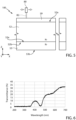
- Figure 6 illustrates, in this regard, experimental data of transmittance after formation of the ohmic-contact layer 60 and exposure of the device 50 to UV radiation at various wavelengths; the behaviour is as expected and is comparable with that of a traditional UV detector.
- Figure 7 illustrates a UV detector device 150 according to a further aspect of the present invention.
- the device 150 does not have the ohmic-contact layer 56 of nickel silicide and the cathode metallization 57. Instead, the device 150 includes an ohmic-contact layer 156, which extends over the surface 53b of the substrate 53.
- the ohmic-contact layer 156 is similar to the ohmic-contact layer 60 (in particular, it can include one or more carbon-rich layers, for example graphite layers or graphene multi-layers) and is transparent to the UV radiation to be detected (e.g., with a wavelength in the range from 200 nm to 380 nm).
- Formation of the ohmic-contact layer 156 includes a laser treatment (similar to what has been discussed previously for formation of the ohmic-contact layer 60).
- optimization of the ohmic properties of the contact 156 at the back of the substrate 53 requires an energy density of the beam 82 different from the energy required for optimization of the ohmic properties of the layer 60 in the implanted region (having a P doping).
- an energy density of the laser beam is required greater than that required for generation of an ohmic contact in a doped region P via the implantation process.
- the response of the detector is maximized thanks to the possibility of exploiting, by photodetection, all the surface available irrespective of the presence of the electrical contacts (which, according to the invention, as has been said, are transparent to the UV radiation to be detected).
- the present invention makes it possible to provide a UV detector designed to detect radiation that impinges upon both surfaces (front and back), which can be used, for example, to manufacture windows of space stations and/or buildings, spectacles, etc.
- the possibility is provided of modulating the shape and dimensions of the area that detects the UV radiation by directing the laser beam according to the need, i.e., without the use of photomasking techniques.
Landscapes
- Light Receiving Elements (AREA)
- Electrodes Of Semiconductors (AREA)
- Photometry And Measurement Of Optical Pulse Characteristics (AREA)
- Carbon And Carbon Compounds (AREA)
- Measurement Of Radiation (AREA)
Abstract
Description
- The present invention relates to a method for manufacturing a UV-radiation detector device and to a UV-radiation detector device. In particular, the present invention relates to a photodetector diode with anode terminal and/or cathode terminal that are transparent to the UV radiation to be detected.
- As is known, semiconductor materials that have a wide bandgap, in particular, an energy value Eg of the bandgap higher than 1.1 eV, low on-state resistance (RON), a high value of thermal conductivity, high operating frequency and high speed of saturation of the charge carriers are ideal for producing electronic components, such as diodes or transistors, in particular for power applications. A material having these characteristics, and designed for being used for manufacturing electronic components, is silicon carbide (SiC). In particular, silicon carbide, in its different polytypes (for example, 3C-SiC, 4H-SiC, 6H-SiC), is preferable to silicon as regards the properties listed previously.
- Electronic devices provided on a silicon-carbide substrate, as compared to similar devices provided on a silicon substrate, present numerous advantages, such as low output on-state resistance, low leakage current, high operating temperature and high operating frequencies. In particular, detection of ultraviolet (UV) radiation, for example coming from the Sun, from astronomic objects, or from artificial sources (in the medical, military, environmental, and astronomical fields) has received a considerable attention in the last few years. The manufacture of arrays of high-sensitivity diodes therefore present particular interest. In this context, wide-band-gap materials are excellent candidates for the detection of UV radiation; silicon carbide is consequently particularly suited for the purpose. Among SiC polytypes, 4H-SiC is preferable for detecting UV radiation, thanks to its wide band gap (approximately 3.3 eV).
- Schottky or PN photodiodes of a known type, for detection of UV radiation, are manufactured on a 4H-SiC epitaxial layer grown on a heavily doped substrate. Schottky contacts are provided on the front of the photodiode by formation of metal regions that provide the Schottky contacts, while an ohmic contact is provided on the back of the photodiode, for example by formation of a nickel layer followed by a fast thermal annealing (at approximately 950-1000°C). The Schottky contacts on the front side are obtained by defining, by lithographic processes, structures of titanium or nickel-silicide that are typically combfingered. The geometry of Schottky contacts on the front side (front electrode) is chosen so as to enable direct exposure to the radiation to be detected and vertical-conduction electrical operation of the Schottky photodiode thus manufactured.
- The area of the single diode directly exposed to UV radiation and electro-optically active is limited by the presence of the front Schottky contacts, which reflect and/or absorb the UV radiation and therefore reduce the useful area effectively exposed.
-
Figure 1 shows, in side cross-sectional view in a (triaxial) cartesian reference system of axes X, Y, Z, a vertical-conduction Schottkydiode 1 of a known type. - The Schottky
diode 1 includes: asubstrate 3 of heavily doped SiC of a N type (e.g., 1·1020 atoms/cm3), provided with asurface 3a opposite to asurface 3b; a drift layer 2 of SiC grown epitaxially on thesurface 3a of thesubstrate 3, having a dopant concentration of an N type lower than the dopant concentration of thesubstrate 3; an ohmic-contact region 6 (for example of nickel silicide), which extends over thesurface 3b of thesubstrate 3; acathode metallization 16, which extends over the ohmic-contact region 6; and ananode metallization 8, which extends over atop surface 2a of the drift layer 2. - Schottky contacts or junctions (of a semiconductor-metal type) are consequently formed at the interface between the drift layer 2 and the
anode metallization 8. In particular, Schottky junctions are formed by portions of the drift layer 2 in direct electrical contact with respective portions of theanode metallization 8. - As has been said, a disadvantage of this device is the reduction of the active area, i.e., of the area dedicated to generation of charge carriers following upon interaction with the UV radiation to be detected. In fact, the portions of the
surface 2a coated by theanode metallization 8 do not participate in the detection of the UV radiation and subsequent generation of the charge carriers on account of absorption and/or reflection of the UV radiation itself to be detected by theanode metallization 8. - The aim of the present invention is to provide a method for manufacturing a UV-radiation detector device, as well as a UV-radiation detector device that will be able to overcome the drawbacks of the prior art.
- According to the present invention a method for manufacturing a UV-radiation detector device and a UV-radiation detector device are provided as defined in the annexed claims.
- For a better understanding of the present invention, preferred embodiments thereof are now described purely to way of non-limiting example with reference to the attached drawings, wherein:
-
Figure 1 is a cross-sectional view of a Schottky photodiode according to a known embodiment; -
Figure 2 is a cross-sectional view of a UV-radiation detector device according to one embodiment of the present invention; -
Figures 3-5 show steps for manufacturing the device ofFigure 2 , according to one embodiment of the present invention; -
Figure 6 illustrates measurements of transmittance of the device manufactured according to the present invention; and -
Figure 7 is a cross-sectional view of a UV-radiation detector device according to a further embodiment of the present invention. -
Figure 2 shows, in side cross-sectional view in a (triaxial) cartesian reference system of axes X, Y, Z, adevice 50, in particular a device for detecting ultraviolet radiation (UV), in particular a PN diode, according to one aspect of the present invention. In this context, thedevice 50 is designed to detect radiation having a wavelength in the 200-nm to 380-nm range. - The
device 50 includes: asubstrate 53, of SiC of an N type, having a first dopant concentration, provided with asurface 53a opposite to asurface 53b, and having a thickness comprised between 50 µm and 350 µm, for example equal to 180 µm; a drift layer (e.g., grown epitaxially) 52, of SiC of an N type, having a second dopant concentration lower than the first dopant concentration, which extends over thesurface 53a of thesubstrate 53 and has a thickness comprised, for example, between 5 and 100 µm; an ohmic-contact region or layer 56 (for example, of nickel silicide), which extends over thesurface 53b of thesubstrate 53; acathode metallization 57, for example of Ti/NiV/Ag or Ti/NiV/Au, which extends over the ohmic-contact region 56; an implantedanode region 59, which extends in thedrift layer 52, facing thetop surface 52a of thedrift layer 52, of a P type; and an ohmic-contact layer 60, which extends in the implantedanode region 59 and faces thetop surface 52a of thedrift layer 52. - The doping level of the
substrate 53 is, for example, comprised between 1·1019 and 1·1022 atoms/cm3; the doping level of thedrift layer 52 is, for example, comprised between 1·1013 and 5·1016 atoms/cm3; the doping level of the implantedanode region 59 is, for example, equal to or higher than to 1·1018 atoms/cm3. - According to one aspect of the present invention, the ohmic-
contact layer 60 includes one or more carbon-rich layers, which comprise, for example, graphite layers, or graphene multi-layers. More in particular, the ohmic-contact layer 60 has, on thesurface 52a, an Si/C amorphous layer in which the carbon atoms are preponderant (for example, at least twice as many, in particular from twice to 100 times as many) as compared to the silicon atoms, following upon a separation of phase between the silicon atoms and the carbon atoms of the SiC substrate. - In particular, in one embodiment of the present invention, said one or more carbon-rich layers can be identified with the following chemical formula: Si(1-x)Cx wherein x is comprised between 0.8 and 1 (in particular 0.8<x≤1).
- Underneath this amorphous layer, the ohmic-
contact layer 60 may present a layer including carbon clusters (e.g., graphite layer), having a thickness greater than that of the amorphous layer. Formation of this ohmic-contact layer 60 is due to a thermal decomposition of silicon carbide, as a result of the manufacturing process illustrated in what follows. - According to a further aspect of the present invention, the ohmic-
contact layer 60 is self-aligned, on thesurface 52a, with the implanted region 59 (i.e., in top view in the plane XY, the ohmic-contact layer 60 has the same shape and extension as the implanted region 59). - In addition, according to a further aspect of the present invention, the ohmic-
contact layer 60 does not extend, along Z, beyond thesurface 52a; in other words, the ohmic-contact layer 60 has a top surface 60a coplanar (i.e., aligned along X) with thesurface 52a, and extends in depth (along Z) in the implantedregion 59 for a depth comprised between one nanometre and some tens of nanometres (e.g., between 1 and 20 nm) measured starting from thesurface 52a. - The shape in plan view, or "layout", of the implanted region 59 (and therefore of the ohmic-contact layer 60) in the plane XY can be chosen according to the need, in the design stage. In particular, the implanted
region 59 can extend continuously (in top view in the plane XY) over the entire active area of thedevice 50, or else only over a portion of the active area of thedevice 50, or else may be formed by a plurality of implanted sub-regions separated from one another by portions of thedrift layer 52. - The present applicant has found that an ohmic-
contact layer 60 of the type described previously is transparent to UV radiation, in particular to radiation with a wavelength in the 200-nm to 380-nm range. Therefore, in use, even in the case where the ohmic-contact layer 60 were to cover the entire active area of thedevice 50, the UV radiation to be detected would traverse in any case the ohmic-contact layer 60, reaching thedrift layer 52 and generating, in a per se known manner, the charge carriers. By appropriately polarizing thedevice 50 between the anode and the cathode (e.g., by bonding wires) it is thus possible to collect and measure a current induced by the UV radiation, in a way in itself known that does not form part of the present invention. - Steps of formation of the
device 50 are described in what follows, only with reference to the steps of formation of the ohmic-contact layer 60 (the remaining steps are carried out according to the prior art). - With reference to
Figure 3 , awafer 100 is arranged, including thesubstrate 53 of SiC (in particular, 4H-SiC; however, other polytypes may be used such as, though not exclusively, 2H-SiC, 3C-SiC and 6H-SiC). - As has been said, the
substrate 53 has a first conductivity type (in this embodiment a doping of an N type) and is provided with thefront surface 53a and theback surface 53b, which are opposite to one another along the axis Z. Thesubstrate 53 has a dopant concentration comprised between 1·1019 and 1·1022 atoms/cm3. - The front of the
wafer 100 corresponds to thefront surface 53a, and the back of thewafer 100 corresponds to theback surface 53b. The resistivity of the substrate 30 is, for example, comprised between 2 mΩ·cm and 40 mΩ·cm. - Formed on the
front surface 53a of thesubstrate 53, for example by epitaxial growth, is thedrift layer 52 of silicon carbide having the first conductivity type (N) and having a dopant concentration lower than that of thesubstrate 53, for example comprised between 1·1013 and 5·1016 atoms/cm3. Thedrift layer 52 is of SiC, in particular 4H-SiC, but it is possible to use other SiC polytypes, such as 2H, 6H, 3C or 15R. - The
drift layer 52 has a thickness defined between atop side 52a and abottom side 52b (the latter being in direct contact with thefront surface 53a of the substrate 53) . - Then (
Figure 4 ), an implantation is performed of dopant species (for example, boron or aluminium), which have the second conductivity type (here, a P conductivity). The implantation (indicated in the figures by arrows 72) can be carried out with or without implantation mask, according to the design requirements, as mentioned previously. In the absence of an implantation mask, an implanted region extends throughout the extension of the plane XY of a cartesian reference system, as indicated in the figures, of thedrift layer 52 and along Z for a depth that depends upon the energy of the implantation itself; in the presence of implantation mask, one or more implanted regions extend where the implantation mask is transparent to the implantation. - In an embodiment provided by way of example, the implantation step of
Figure 4 comprises one or more implantations of dopant species, which have the second conductivity type, with implantation energy comprised between 30 keV and 500 keV, and with doses of between 1·1012 atoms/cm2 and 1·1015 atoms/cm2. A subsequent thermal annealing enables activation of the dopants thus implanted and form the implantedanode region 59 with a dopant concentration of higher than 1·1018 atoms/cm3 and depth, measured starting from thesurface 52a, comprised between 0.3 µm and 1 µm. - Next (
Figure 5 ), generated on thesurface 52a is a thermal budget designed to favour generation, in the implantedregion 59, of the aforementioned one or more carbon-rich layers (for example, graphene and/or graphite layers). - For this purpose, a
laser source 80 is used, configured to generate anappropriate beam 82. - The
laser 80 is, for example, a UV excimer laser. Other types of laser may be used, amongst which lasers with a wavelength in the region of the visible. - The configuration and operating parameters of the
laser 80, optimized for achieving the purpose of the present invention, i.e., for enabling formation of an ohmic contact in the implantedregion 59, are the following: - wavelength: between 290 and 370 nm, in particular 310 nm;
- pulse duration: between 100 ns and 300 ns, in particular 160 ns;
- number of pulses (scans): between 1 and 5;
- energy density: between 1.5 J/cm2 and 4 J/cm2, in particular 3 J/cm2 (considered at the level of the
surface 52a); and - temperature: between 1400°C and 2600°C, in particular 1800°C (considered at the level of the
surface 52a). - The area of the spot of the
beam 82 at the level of thesurface 52a is, for example, comprised between 0.7 and 1.5 cm2. - In order to cover the
entire wafer 100, or the subregion of thewafer 100 to be heated, one or more scans of thelaser 80 are therefore performed in the plane XY (e.g., a plurality of scans parallel to one another and to the axis X and/or axis Y). - Given the depth of the implanted
region 59, a temperature of approximately 2000°C at the level of thesurface 52a is sufficient to guarantee temperatures within the range identified above also at the maximum depth reached by the implanted region 59 (e.g., 1 µm) so as to guarantee activation of all the dopant without the need to carry out a dedicated thermal budget. - This temperature is such as to favour generation of compounds of the carbon-rich ohmic contacts exclusively in the implanted
region 59, and not at thesurface 52a without the implantedregion 59. This effect, of a type in itself known, is described, for example, by Maxime G. Lemaitre, "Low-temperature, site selective graphitization of SiC via ion implantation and pulsed laser annealing", ). - In one embodiment, transformation of part of the implanted
region 59 into the ohmic-contact layer 60 is obtained by heating theentire wafer 100, appropriately moving thelaser 80. With an energy density of thebeam 82 comprised between 1.5 and 3 J/cm2, the localized and surface increase of the temperature causes formation of the ohmic-contact layer 60. Where the implantedregion 59 is not present, this effect is not observed. - In a different embodiment, transformation of the surface portion of the implanted
region 59 into the ohmic-contact layer 60 is obtained by treating only a part of thewafer 100, which might not correspond to the entire extension of the implanted region 59 (for example, excluding possible portions that are not of interest during use of thedevice 50 as UV detector in so far as they do not take part in generation and transport of electric charge). - In a further embodiment, it is possible to arrange on the
surface 52a (either in contact with thesurface 52a or at a distance therefrom) a mask having one or more regions transparent to the beam 82 (i.e., thebeam 82 traverses them) and regions opaque to the beam 82 (i.e., thebeam 82 does not traverse them, or traverses them in attenuated form such as not to heat significantly the portions of thewafer 100 that extend underneath it). The transparent regions of the mask that are aligned to the implanted region 59 (or to respective implanted regions) enable formation of the respective ohmic-contact layer 60. Possible regions of thedrift layer 52 without the P implantation are covered and protected by the mask. In this case, the energy density of thebeam 82 can be increased up to 4.5 J/cm2 or more. In fact, to generate an ohmic contact in doped regions during epitaxial growth, an energy density of the laser beam is required higher than the one required for generation of an ohmic contact in doped regions through the ion-implantation process (in particular, higher than approximately 3 J/cm2). - In this embodiment, since a mask is present that exposes only the implanted
regions 59, it is possible to use energy densities of higher than 3 J/cm2, without the risk of forming an ohmic contact on regions of an N type of thedrift layer 52. - The step of thermal annealing for activation of the dopants of the implanted
region 59 may, in one embodiment, coincide with the step of formation of the ohmic-contact layer 60 in so far as the temperature reached by thelaser beam 82 is such as to activate the dopants. Alternatively, it is in any case possible to carry out traditional thermal annealing prior to formation of the ohmic-contact layer 60. - Transformation of the SiC of a P type into the ohmic contact occurs at temperatures comprised between 1200°C and 2600°C, more in particular temperatures higher than of 1600°C. These temperatures are reached in a surface portion (some nanometres, e.g., 1-20 nm) of the implanted
region 59. - For greater depths, the temperature drops to values such as not to cause any longer transformation of silicon carbide into carbon-rich layers (graphene and/or graphite layers).
- Formation of the ohmic contact is therefore self-limited. Consequently, the ohmic-
contact layer 60 does not extend throughout the thickness of the respective implanted region, but exclusively at the surface level thereof. The ohmic-contact layer 60 is formed within the implantedregion 59 such that a top surface of the implantedregion 59 is coplanar or otherwise coinciding with a top surface of the ohmic-contact layer 60. - The present applicant has found that, with the parameters of laser configuration and operation identified previously, the desired electrical and optical behaviour for the
device 50 is obtained.Figure 6 illustrates, in this regard, experimental data of transmittance after formation of the ohmic-contact layer 60 and exposure of thedevice 50 to UV radiation at various wavelengths; the behaviour is as expected and is comparable with that of a traditional UV detector. -
Figure 7 illustrates aUV detector device 150 according to a further aspect of the present invention. - Elements of the
device 150 common to thedevice 50 ofFigure 2 are designated by the same reference numbers and are not described any further. - Unlike the
device 50, thedevice 150 does not have the ohmic-contact layer 56 of nickel silicide and thecathode metallization 57. Instead, thedevice 150 includes an ohmic-contact layer 156, which extends over thesurface 53b of thesubstrate 53. The ohmic-contact layer 156 is similar to the ohmic-contact layer 60 (in particular, it can include one or more carbon-rich layers, for example graphite layers or graphene multi-layers) and is transparent to the UV radiation to be detected (e.g., with a wavelength in the range from 200 nm to 380 nm). - Formation of the ohmic-
contact layer 156 includes a laser treatment (similar to what has been discussed previously for formation of the ohmic-contact layer 60). - Optimization of the ohmic properties of the
contact 156 at the back of the substrate 53 (having an N doping) requires an energy density of thebeam 82 different from the energy required for optimization of the ohmic properties of thelayer 60 in the implanted region (having a P doping). In fact, as has been said, to generate an ohmic contact on the substrate having an N doping an energy density of the laser beam is required greater than that required for generation of an ohmic contact in a doped region P via the implantation process. For this purpose, it is possible to regulate operating parameters of thelaser 80 to generate beams with different characteristics according to the ohmic-contact layer - It is consequently also possible to use the
laser 80, with the following configuration and operating parameters, to form theohmic contact 156 at the back 53b of thesubstrate 53, namely: - wavelength: between 290 and 370 nm, in particular 310 nm;
- pulse duration: between 100 ns and 300 ns, in particular 160 ns;
- number of pulses (scans): between 1 and 5;
- energy density: between 3 and 4.5 J/cm2, in particular between 3.2 J/cm2 and 4.5 J/cm2;
- temperature: between 1400°C and 2600°C, in particular higher than 1800°C (considered at the level of the
surface 53b) . - In this way a UV detector is obtained capable of receiving the UV radiation from both sides (front and back).
- From an examination of the characteristics of the invention provided according to the present disclosure the advantages that it affords are evident.
- In particular, the response of the detector is maximized thanks to the possibility of exploiting, by photodetection, all the surface available irrespective of the presence of the electrical contacts (which, according to the invention, as has been said, are transparent to the UV radiation to be detected).
- In addition, the manufacturing process flow is simplified as compared to the prior art.
- Moreover, the present invention makes it possible to provide a UV detector designed to detect radiation that impinges upon both surfaces (front and back), which can be used, for example, to manufacture windows of space stations and/or buildings, spectacles, etc.
- Furthermore, according to the present invention, the possibility is provided of modulating the shape and dimensions of the area that detects the UV radiation by directing the laser beam according to the need, i.e., without the use of photomasking techniques.
- Finally, it is clear that modifications and variations may be made to what has been described and illustrated herein, without with thereby departing from the scope of the present invention, as defined in the annexed claims.
Claims (12)
- A detector device (50; 150) for detecting UV radiation, comprising:- a SiC substrate (53) having a first conductivity (N) and a first concentration of dopant species, provided with a front side (53a) and a back side (53b) opposite to one another;- a SiC drift layer (52), which extends over the front side (53a) of the substrate (53), having the first conductivity (N) and a second concentration of dopant species lower than the first concentration;- a cathode terminal on the back side of the substrate (53); and- an anode terminal in the drift layer (52),characterized in that the anode terminal comprises:- a doped anode region (59) in the drift layer (52), including dopant species having a second conductivity (P) opposite to the first conductivity (N);- a first ohmic-contact region (60) including one or more carbon-rich layers, which extends in said doped anode region (59).
- The device according to claim 1, wherein the doped anode region (59) extends in depth in the drift layer (52) starting from a top surface (52a) of the drift layer (52),
and wherein said first ohmic-contact region (60) has a top surface thereof coinciding with said top surface (52a) of the drift layer (52). - The device according to claim 1 or claim 2, wherein the first ohmic-contact region (60) comprises said one or more carbon-rich layers exclusively within the doped anode region (59).
- The device according to anyone of claims 1 to 3, wherein said first ohmic-contact region (60) extends in the doped anode region (59) for a depth comprised between 1 nm and 20 nm.
- The device according to anyone of claims 1 to 3, wherein said substrate (53) is of 4H-SiC.
- The device according to anyone of claims 1 to 3, wherein the cathode terminal comprises a second ohmic-contact region (156) including one or more carbon-rich layers, in particular graphene and/or graphite layers, which extends in said doped anode region (59).
- The device according to claim 6, wherein the second ohmic-contact region (156) has a surface thereof coinciding with the back side (53b) of the substrate (53).
- The device according to anyone of claims 1 to 7, wherein said carbon-rich layers comprise graphene and/or graphite layers.
- The device according to anyone of claims 1 to 7, wherein said carbon-rich layers comprise graphite layers or graphene multi-layers.
- The device according to anyone of claims 1 to 9, wherein the first ohmic-contact region (60) has, at the top surface (52a), a Si/C amorphous layer in which the Carbon atoms are preponderant as compared to the Silicon atoms.
- The device according to claim 10, wherein the Carbon atoms are in a number ranging from twice to 100 times as Silicon atoms.
- The device according to anyone of claims 1 to 11, wherein said one or more carbon-rich layers are identified with the following chemical formula: Si(1-x)Cx, wherein x is comprised between 0.8 and 1, more in particular 0.8<x≤1.
Applications Claiming Priority (2)
| Application Number | Priority Date | Filing Date | Title |
|---|---|---|---|
| IT102020000015100A IT202000015100A1 (en) | 2020-06-23 | 2020-06-23 | METHOD OF MANUFACTURING SIC-BASED UV RADIATION DETECTOR AND SIC-BASED UV RADIATION DETECTOR |
| EP21180942.1A EP3930010B1 (en) | 2020-06-23 | 2021-06-22 | Method for manufacturing a uv-radiation detector device based on sic, and uv-radiation detector device based on sic |
Related Parent Applications (2)
| Application Number | Title | Priority Date | Filing Date |
|---|---|---|---|
| EP21180942.1A Division-Into EP3930010B1 (en) | 2020-06-23 | 2021-06-22 | Method for manufacturing a uv-radiation detector device based on sic, and uv-radiation detector device based on sic |
| EP21180942.1A Division EP3930010B1 (en) | 2020-06-23 | 2021-06-22 | Method for manufacturing a uv-radiation detector device based on sic, and uv-radiation detector device based on sic |
Publications (2)
| Publication Number | Publication Date |
|---|---|
| EP4322229A2 true EP4322229A2 (en) | 2024-02-14 |
| EP4322229A3 EP4322229A3 (en) | 2024-05-22 |
Family
ID=72473758
Family Applications (2)
| Application Number | Title | Priority Date | Filing Date |
|---|---|---|---|
| EP21180942.1A Active EP3930010B1 (en) | 2020-06-23 | 2021-06-22 | Method for manufacturing a uv-radiation detector device based on sic, and uv-radiation detector device based on sic |
| EP23220528.6A Pending EP4322229A3 (en) | 2020-06-23 | 2021-06-22 | Method for manufacturing a uv-radiation detector device based on sic, and uv-radiation detector device based on sic |
Family Applications Before (1)
| Application Number | Title | Priority Date | Filing Date |
|---|---|---|---|
| EP21180942.1A Active EP3930010B1 (en) | 2020-06-23 | 2021-06-22 | Method for manufacturing a uv-radiation detector device based on sic, and uv-radiation detector device based on sic |
Country Status (5)
| Country | Link |
|---|---|
| US (2) | US11605751B2 (en) |
| EP (2) | EP3930010B1 (en) |
| JP (1) | JP7782972B2 (en) |
| CN (2) | CN215680707U (en) |
| IT (1) | IT202000015100A1 (en) |
Families Citing this family (5)
| Publication number | Priority date | Publication date | Assignee | Title |
|---|---|---|---|---|
| IT202000004696A1 (en) | 2020-03-05 | 2021-09-05 | St Microelectronics Srl | MANUFACTURING METHOD OF AN ELECTRONIC DEVICE IN SiC WITH REDUCED HANDLING PHASES, AND ELECTRONIC DEVICE IN SiC |
| IT202000008179A1 (en) | 2020-04-17 | 2021-10-17 | St Microelectronics Srl | FORMATION OF OHMIC CONTACTS IN A SIC BASED ELECTRONIC DEVICE, AND ELECTRONIC DEVICE |
| IT202000008167A1 (en) | 2020-04-17 | 2021-10-17 | St Microelectronics Srl | DRUG ACTIVATION AND FORMATION OF OHMIC CONTACT IN AN ELECTRONIC DEVICE IN SIC, AND ELECTRONIC DEVICE IN SIC |
| IT202000015100A1 (en) * | 2020-06-23 | 2021-12-23 | St Microelectronics Srl | METHOD OF MANUFACTURING SIC-BASED UV RADIATION DETECTOR AND SIC-BASED UV RADIATION DETECTOR |
| US12593485B2 (en) * | 2022-03-18 | 2026-03-31 | Stmicroelectronics S.R.L. | Forming an electronic device, such as a JBS or MPS diode, based on 3C—SiC, and 3C—SiC electronic device |
Family Cites Families (40)
| Publication number | Priority date | Publication date | Assignee | Title |
|---|---|---|---|---|
| JP2001244496A (en) * | 2000-03-02 | 2001-09-07 | Matsushita Electric Ind Co Ltd | Photodetector |
| US6747291B1 (en) * | 2003-01-10 | 2004-06-08 | The United States Of America As Represented By The Secretary Of The Air Force | Ohmic contacts on p-type silicon carbide using carbon films |
| US20050104072A1 (en) * | 2003-08-14 | 2005-05-19 | Slater David B.Jr. | Localized annealing of metal-silicon carbide ohmic contacts and devices so formed |
| US6974720B2 (en) * | 2003-10-16 | 2005-12-13 | Cree, Inc. | Methods of forming power semiconductor devices using boule-grown silicon carbide drift layers and power semiconductor devices formed thereby |
| US7498633B2 (en) | 2005-01-21 | 2009-03-03 | Purdue Research Foundation | High-voltage power semiconductor device |
| WO2007035333A1 (en) | 2005-09-16 | 2007-03-29 | Cree, Inc. | Methods of processing semiconductor wafers having silicon carbide power devices thereon |
| DE102006050360B4 (en) | 2006-10-25 | 2014-05-15 | Infineon Technologies Austria Ag | Method for generating an electrical contact on SiC |
| US8232558B2 (en) | 2008-05-21 | 2012-07-31 | Cree, Inc. | Junction barrier Schottky diodes with current surge capability |
| JP5449786B2 (en) | 2009-01-15 | 2014-03-19 | 昭和電工株式会社 | Silicon carbide semiconductor device and method for manufacturing silicon carbide semiconductor device |
| JP2011071281A (en) | 2009-09-25 | 2011-04-07 | Toyota Central R&D Labs Inc | Semiconductor device and method of manufacturing the same |
| JP5175872B2 (en) | 2010-01-21 | 2013-04-03 | 株式会社東芝 | Semiconductor rectifier |
| JP5803934B2 (en) * | 2011-07-20 | 2015-11-04 | 住友電気工業株式会社 | Silicon carbide substrate, semiconductor device and manufacturing method thereof |
| US8664665B2 (en) | 2011-09-11 | 2014-03-04 | Cree, Inc. | Schottky diode employing recesses for elements of junction barrier array |
| JP2014063948A (en) | 2012-09-24 | 2014-04-10 | Sumitomo Electric Ind Ltd | Silicon carbide semiconductor device manufacturing method |
| US9425153B2 (en) | 2013-04-04 | 2016-08-23 | Monolith Semiconductor Inc. | Semiconductor devices comprising getter layers and methods of making and using the same |
| WO2014199510A1 (en) * | 2013-06-14 | 2014-12-18 | 新電元工業株式会社 | Method for manufacturing semiconductor device and semiconductor device |
| JP5846178B2 (en) | 2013-09-30 | 2016-01-20 | サンケン電気株式会社 | Semiconductor device and manufacturing method thereof |
| JP6135537B2 (en) | 2014-02-10 | 2017-05-31 | トヨタ自動車株式会社 | Semiconductor device using SiC substrate and method for manufacturing the same |
| US8962468B1 (en) | 2014-04-23 | 2015-02-24 | United Silicon Carbide, Inc. | Formation of ohmic contacts on wide band gap semiconductors |
| CN106463541B (en) | 2014-05-23 | 2019-05-21 | 松下知识产权经营株式会社 | Silicon carbide semiconductor device |
| CN204966510U (en) | 2014-06-20 | 2016-01-13 | 意法半导体股份有限公司 | Wide Bandgap High Density Semiconductor Switching Devices |
| EP3076422B1 (en) * | 2014-07-02 | 2018-10-31 | Fuji Electric Co., Ltd. | Silicon carbide semiconductor element production method |
| JP2016046449A (en) | 2014-08-26 | 2016-04-04 | 住友重機械工業株式会社 | Semiconductor element manufacturing method |
| US9966491B2 (en) * | 2015-02-20 | 2018-05-08 | University Of South Carolina | Optically switched graphene/4H-SiC junction bipolar transistor |
| CN107534054B (en) | 2015-04-22 | 2020-08-18 | 三菱电机株式会社 | Semiconductor device and method of manufacturing the same |
| US9917170B2 (en) * | 2016-04-22 | 2018-03-13 | Infineon Technologies Ag | Carbon based contact structure for silicon carbide device technical field |
| US20180019309A1 (en) | 2016-07-15 | 2018-01-18 | Global Power Technologies Group, Inc. | Semiconductor device based on wideband gap semiconductor materials |
| DE102016124973A1 (en) | 2016-12-20 | 2018-06-21 | Infineon Technologies Ag | Semiconductor devices and methods of forming semiconductor devices |
| DE102017100109A1 (en) | 2017-01-04 | 2018-07-05 | Infineon Technologies Ag | SEMICONDUCTOR DEVICE AND METHOD FOR MANUFACTURING THE SAME |
| JP6926869B2 (en) | 2017-09-13 | 2021-08-25 | 富士電機株式会社 | Semiconductor device |
| CN108257856B (en) * | 2017-12-21 | 2019-05-24 | 秦皇岛京河科学技术研究院有限公司 | Preparation method and structure of SiC MOSFET power device with high temperature resistance and low power consumption |
| US10629686B2 (en) | 2018-08-02 | 2020-04-21 | Semiconductor Components Industries, Llc | Carbon-controlled ohmic contact layer for backside ohmic contact on a silicon carbide power semiconductor device |
| CN109326657A (en) * | 2018-08-29 | 2019-02-12 | 北京时代民芯科技有限公司 | A kind of silicon carbide-based ultraviolet detector and preparation method thereof |
| CN109037041A (en) | 2018-09-21 | 2018-12-18 | 黄兴 | A kind of preparation method and device of the Ohmic contact of silicon carbide |
| JP7225873B2 (en) | 2019-02-07 | 2023-02-21 | 富士電機株式会社 | Semiconductor device and method for manufacturing semiconductor device |
| EP3712962B1 (en) | 2019-03-22 | 2023-06-07 | STMicroelectronics S.r.l. | Semiconductor mps diode with reduced current-crowding effect and manufacturing method thereof |
| IT202000004696A1 (en) | 2020-03-05 | 2021-09-05 | St Microelectronics Srl | MANUFACTURING METHOD OF AN ELECTRONIC DEVICE IN SiC WITH REDUCED HANDLING PHASES, AND ELECTRONIC DEVICE IN SiC |
| IT202000008179A1 (en) | 2020-04-17 | 2021-10-17 | St Microelectronics Srl | FORMATION OF OHMIC CONTACTS IN A SIC BASED ELECTRONIC DEVICE, AND ELECTRONIC DEVICE |
| IT202000008167A1 (en) | 2020-04-17 | 2021-10-17 | St Microelectronics Srl | DRUG ACTIVATION AND FORMATION OF OHMIC CONTACT IN AN ELECTRONIC DEVICE IN SIC, AND ELECTRONIC DEVICE IN SIC |
| IT202000015100A1 (en) * | 2020-06-23 | 2021-12-23 | St Microelectronics Srl | METHOD OF MANUFACTURING SIC-BASED UV RADIATION DETECTOR AND SIC-BASED UV RADIATION DETECTOR |
-
2020
- 2020-06-23 IT IT102020000015100A patent/IT202000015100A1/en unknown
-
2021
- 2021-06-10 US US17/344,558 patent/US11605751B2/en active Active
- 2021-06-21 JP JP2021102346A patent/JP7782972B2/en active Active
- 2021-06-22 EP EP21180942.1A patent/EP3930010B1/en active Active
- 2021-06-22 CN CN202121388481.XU patent/CN215680707U/en active Active
- 2021-06-22 CN CN202110693664.0A patent/CN113903825B/en active Active
- 2021-06-22 EP EP23220528.6A patent/EP4322229A3/en active Pending
-
2023
- 2023-03-09 US US18/181,409 patent/US12125933B2/en active Active
Non-Patent Citations (1)
| Title |
|---|
| MAXIME G. LEMAITRE: "Low-temperature, site selective graphitization of SiC via ion implantation and pulsed laser annealing", APPLIED PHYSICS LETTERS, vol. 100, 2012, pages 193105, XP012155967, DOI: 10.1063/1.4707383 |
Also Published As
| Publication number | Publication date |
|---|---|
| CN215680707U (en) | 2022-01-28 |
| US11605751B2 (en) | 2023-03-14 |
| CN113903825A (en) | 2022-01-07 |
| CN113903825B (en) | 2025-10-28 |
| IT202000015100A1 (en) | 2021-12-23 |
| EP3930010C0 (en) | 2024-02-21 |
| JP2022003685A (en) | 2022-01-11 |
| US20210399154A1 (en) | 2021-12-23 |
| EP3930010B1 (en) | 2024-02-21 |
| US12125933B2 (en) | 2024-10-22 |
| EP4322229A3 (en) | 2024-05-22 |
| US20230282757A1 (en) | 2023-09-07 |
| EP3930010A1 (en) | 2021-12-29 |
| JP7782972B2 (en) | 2025-12-09 |
Similar Documents
| Publication | Publication Date | Title |
|---|---|---|
| US11605751B2 (en) | Method for manufacturing a UV-radiation detector device based on SiC, and UV-radiation detector device based on SiC | |
| US12051725B2 (en) | Doping activation and ohmic contact formation in a SiC electronic device, and SiC electronic device | |
| EP3896720B1 (en) | Ohmic contact formation in a sic-based electronic device, and electronic device | |
| JP5104314B2 (en) | Semiconductor device and manufacturing method thereof | |
| US20180323261A1 (en) | Silicon carbide semiconductor device and method for producing same | |
| EP4095927A1 (en) | Method of manufacturing super junction, and super junction schottky diode using same | |
| US20110306188A1 (en) | Manufacturing method of silicon carbide semiconductor device | |
| WO2016091488A1 (en) | Method for manufacturing a wide bandgap junction barrier schottky diode | |
| JP2001156299A (en) | Semiconductor device and manufacturing method thereof | |
| IT202100002333A1 (en) | JBS DEVICE WITH IMPROVED ELECTRICAL PERFORMANCE, AND JBS DEVICE MANUFACTURING PROCESS | |
| RU174126U1 (en) | Diamond Schottky Barrier Diode | |
| CN112382670B (en) | Avalanche diode based on high-purity intrinsic monocrystalline diamond and preparation method | |
| Tian et al. | Laser direct write doping and metallization fabrication of silicon carbide PIN diodes | |
| JP5333241B2 (en) | Manufacturing method of semiconductor device | |
| RU160937U1 (en) | INTEGRATED SCHOTKI p-n DIODE | |
| TR202011952A2 (en) | HOT ELECTRON BASED LOGIC LIGHT EMITTING DEVICE PRODUCING SURFACE GRADIATION |
Legal Events
| Date | Code | Title | Description |
|---|---|---|---|
| PUAI | Public reference made under article 153(3) epc to a published international application that has entered the european phase |
Free format text: ORIGINAL CODE: 0009012 |
|
| STAA | Information on the status of an ep patent application or granted ep patent |
Free format text: STATUS: THE APPLICATION HAS BEEN PUBLISHED |
|
| AC | Divisional application: reference to earlier application |
Ref document number: 3930010 Country of ref document: EP Kind code of ref document: P |
|
| AK | Designated contracting states |
Kind code of ref document: A2 Designated state(s): AL AT BE BG CH CY CZ DE DK EE ES FI FR GB GR HR HU IE IS IT LI LT LU LV MC MK MT NL NO PL PT RO RS SE SI SK SM TR |
|
| REG | Reference to a national code |
Ref country code: DE Ref legal event code: R079 Free format text: PREVIOUS MAIN CLASS: H01L0031105000 Ipc: H01L0031022400 |
|
| PUAL | Search report despatched |
Free format text: ORIGINAL CODE: 0009013 |
|
| AK | Designated contracting states |
Kind code of ref document: A3 Designated state(s): AL AT BE BG CH CY CZ DE DK EE ES FI FR GB GR HR HU IE IS IT LI LT LU LV MC MK MT NL NO PL PT RO RS SE SI SK SM TR |
|
| RIC1 | Information provided on ipc code assigned before grant |
Ipc: H01L 31/18 20060101ALI20240416BHEP Ipc: H01L 31/105 20060101ALI20240416BHEP Ipc: H01L 31/0224 20060101AFI20240416BHEP |
|
| STAA | Information on the status of an ep patent application or granted ep patent |
Free format text: STATUS: REQUEST FOR EXAMINATION WAS MADE |
|
| 17P | Request for examination filed |
Effective date: 20241121 |
|
| RBV | Designated contracting states (corrected) |
Designated state(s): AL AT BE BG CH CY CZ DE DK EE ES FI FR GB GR HR HU IE IS IT LI LT LU LV MC MK MT NL NO PL PT RO RS SE SI SK SM TR |