EP4318953A1 - Complementary current-steering digital-to-analog converter - Google Patents
Complementary current-steering digital-to-analog converter Download PDFInfo
- Publication number
- EP4318953A1 EP4318953A1 EP23183733.7A EP23183733A EP4318953A1 EP 4318953 A1 EP4318953 A1 EP 4318953A1 EP 23183733 A EP23183733 A EP 23183733A EP 4318953 A1 EP4318953 A1 EP 4318953A1
- Authority
- EP
- European Patent Office
- Prior art keywords
- input terminal
- current sources
- type current
- digital
- tia
- Prior art date
- Legal status (The legal status is an assumption and is not a legal conclusion. Google has not performed a legal analysis and makes no representation as to the accuracy of the status listed.)
- Pending
Links
Images



Classifications
-
- H—ELECTRICITY
- H03—ELECTRONIC CIRCUITRY
- H03M—CODING; DECODING; CODE CONVERSION IN GENERAL
- H03M1/00—Analogue/digital conversion; Digital/analogue conversion
- H03M1/66—Digital/analogue converters
- H03M1/74—Simultaneous conversion
-
- H—ELECTRICITY
- H03—ELECTRONIC CIRCUITRY
- H03M—CODING; DECODING; CODE CONVERSION IN GENERAL
- H03M1/00—Analogue/digital conversion; Digital/analogue conversion
- H03M1/66—Digital/analogue converters
- H03M1/74—Simultaneous conversion
- H03M1/742—Simultaneous conversion using current sources as quantisation value generators
-
- H—ELECTRICITY
- H03—ELECTRONIC CIRCUITRY
- H03M—CODING; DECODING; CODE CONVERSION IN GENERAL
- H03M1/00—Analogue/digital conversion; Digital/analogue conversion
- H03M1/06—Continuously compensating for, or preventing, undesired influence of physical parameters
- H03M1/0617—Continuously compensating for, or preventing, undesired influence of physical parameters characterised by the use of methods or means not specific to a particular type of detrimental influence
- H03M1/0675—Continuously compensating for, or preventing, undesired influence of physical parameters characterised by the use of methods or means not specific to a particular type of detrimental influence using redundancy
- H03M1/0678—Continuously compensating for, or preventing, undesired influence of physical parameters characterised by the use of methods or means not specific to a particular type of detrimental influence using redundancy using additional components or elements, e.g. dummy components
- H03M1/068—Continuously compensating for, or preventing, undesired influence of physical parameters characterised by the use of methods or means not specific to a particular type of detrimental influence using redundancy using additional components or elements, e.g. dummy components the original and additional components or elements being complementary to each other, e.g. CMOS
Definitions
- the present invention relates to digital-to-analog converters (DACs), and, in particular, to a current-steering DAC.
- DACs digital-to-analog converters
- a low-noise DAC with a small circuit size and high power performance is called for.
- a complementary current-steering digital-to-analog converter (DAC) is introduced.
- a complementary current-steering DAC in accordance with an exemplary embodiment of the present invention includes a transimpedance amplifier (TIA), a p-type DAC, and an n-type DAC.
- the p-type DAC has a plurality of p-type current sources.
- the p-type current sources are coupled to a first input terminal or a second input terminal of the TIA according to the digital input of the complementary current-steering DAC.
- the n-type DAC has a plurality of n-type current sources.
- the n-type current sources are coupled to the first input terminal or the second input terminal of the TIA according to the digital input of the complementary current-steering DAC.
- one or more n-type current sources connected to the second input terminal of the TIA are switched so that they are connected to the first input terminal of the TIA.
- one or more p-type current sources connected to the first input terminal of the TIA are switched so that they are connected to the second input terminal of the TIA.
- one or more p-type current sources connected to the first input terminal of the TIA are switched so that they are connected to the second input terminal of the TIA, and one or more of the n-type current sources connected to the second input terminal of the TIA are switched so that they are connected to the first input terminal of the TIA.
- the digital input is N bits, wherein N is a number.
- the number of p-type current sources is 2 (N-1) -1.
- the number of n-type current sources is 2 (N-1) .
- the 2 (N-1) -1 p-type current sources are connected to the first input terminal of the TIA, and the 2 (N-1) n-type current sources are connected to the second input terminal of the TIA.
- the 2 (N-1) -1 p-type current sources are connected to the second input terminal of the TIA, and the 2 (N-1) n-type current sources are connected to the first input terminal of the TIA.
- the greater the digital input is the more n-type current sources are connected to the first input terminal of the TIA, and the 2 (N-1) -1 p-type current sources are kept connected to the first input terminal of the TIA.
- the greater the digital input is the more n-type current sources are connected to the first input terminal of the TIA, and the 2 (N-1) -1 p-type current sources are kept connected to the second input terminal of the TIA.
- the complementary current-steering DAC further has a binary weighted circuit coupled to the second input terminal of the TIA to provide a fixed current.
- the p-type current sources each output the fixed current
- the n-type current sources each output the fixed current.
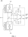
- FIG. 1 illustrates a complementary current-steering digital-to-analog converter (DAC) 100 in accordance with an exemplary embodiment of the present invention.
- the complementary current-steering DAC 100 has a transimpedance amplifier (abbreviated as TIA) 102, a p-type digital-to-analog converter (abbreviated as PDAC) 104, and an n-type digital-to-analog converter (abbreviated as NDAC) 106.
- the TIA 102 may be known as a low-pass filter.
- the PDAC 104 has a plurality of p-type current sources (e.g., implemented by PMOSs).
- the p-type current sources are coupled to a first input terminal n1 or a second input terminal n2 of the TIA 102 according to the digital input IN of the complementary current-steering DAC 100.
- the NDAC 106 has a plurality of n-type current sources (e.g., implemented by NMOSs).
- the n-type current sources are coupled to the first input terminal n1 or the second input terminal n2 of the TIA 102 according to the digital input IN of the complementary current-steering DAC 100.
- the NDAC 106 form the complementary current-steering structure with the PDAC 104.
- the fewer current sources are required and the circuit size is considerably reduced.
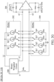
- FIGs 2A to 2H show how a 3-bit DAC 200 works in accordance with an exemplary embodiment of the present invention.
- the 3-bit DAC 200 has three (2 (3-1) -1) p-type current sources Ip1, Ip2 and Ip3 in the PDAC 202, and has four (2 (3-1) ) n-type current sources In1, In2, In3, and In4 in the NDAC 204. Switches are provided within the PDAC 202 and NDAC 204 to determine how to connect the p-type current sources Ip1 ⁇ Ip3 and the n-type current sources In1 ⁇ In4 to the first input terminal n1 or the second input terminal n2 of the TIA 206 according to the digital input IN of the 3-bit DAC 200.
- the 3-bit DAC 200 further has a binary weighted circuit 208, which has a first output terminal t1 coupled to the second input terminal n2 of the TIA 206, and a second output terminal t2 coupled to the first input terminal n1 of the TIA 206.
- the binary weighted circuit 208 uses the first output terminal t1 to output a fixed current (64x, multiple of a base current 1x). Furthermore, the p-type current sources each output the fixed current (64x), and the n-type current sources each output the fixed current (64x).
- the digital input IN is 3b' 000.
- the p-type current sources Ip1 ⁇ Ip3 are all connected to the first input terminal n1 of the TIA 206, and the n-type current sources In1 ⁇ In4 are all connected to the second input terminal n2 of the TIA 206.
- the current from the first node n1 to the output port of the TIA 206 is (64x) ⁇ 3.
- the current from the output port of the TIA 206 to the second node n2 is (64x) ⁇ 4 - 64x.
- the digital input IN is 3b' 001.
- the p-type current sources Ip1 ⁇ Ip3 are all connected to the first input terminal n1 of the TIA 206, the n-type current source In1 is connected to the first input terminal n1 of the TIA 206, and the n-type current sources In2 ⁇ In4 are connected to the second input terminal n2 of the TIA 206.
- the current from the first node n1 to the output port of the TIA 206 is (64x) ⁇ 2.
- the current from the output port of the TIA 206 to the second node n2 is (64x) ⁇ 3 - 64x.
- the digital input IN is 3b' 010.
- the p-type current sources Ip1 ⁇ Ip3 are all connected to the first input terminal n1 of the TIA 206
- the n-type current sources In1 and In2 are connected to the first input terminal n1 of the TIA 206
- the n-type current sources In3 and In4 are connected to the second input terminal n2 of the TIA 206.
- the current from the first node n1 to the output port of the TIA 206 is (64x) ⁇ 1.
- the current from the output port of the TIA 206 to the second node n2 is (64x) ⁇ 2 - 64x.
- the digital input IN is 3b' 011.
- the p-type current source Ip1 is connected to the second input terminal n2 of the TIA 206
- the p-type current sources Ip2 and Ip3 are connected to the first input terminal n1 of the TIA 206
- the n-type current sources In1 and In2 are connected to the first input terminal n1 of the TIA 206
- the n-type current sources In3 and In4 are connected to the second input terminal n2 of the TIA 206.
- the current from the first node n1 to the output port of the TIA 206 is (64x) ⁇ 0.
- the current from the output port of the TIA 206 to the second node n2 is (64x) ⁇ 1 - 64x.
- the digital input IN is 3b' 100.
- the p-type current sources Ip1 and Ip2 are connected to the second input terminal n2 of the TIA 206
- the p-type current source Ip3 is connected to the first input terminal n1 of the TIA 206
- the n-type current sources In1 and In2 are connected to the first input terminal n1 of the TIA 206
- the n-type current sources In3 and In4 are connected to the second input terminal n2 of the TIA 206.
- the current direction is changed in comparison with FIGs 2A-2D .
- the current from the output port of the TIA 206 to the first node n1 is (64x) ⁇ 1.
- the current from the second node n2 to the output port of the TIA 206 to is (64x) ⁇ 0 + 64x.
- the digital input IN is 3b' 101.
- the p-type current sources Ip1 ⁇ Ip3 are all connected to the second input terminal n2 of the TIA 206, the n-type current sources In1 and In2 are connected to the first input terminal n1 of the TIA 206, and the n-type current sources In3 and In4 are connected to the second input terminal n2 of the TIA 206.
- the current from the output port of the TIA 206 to the first node n1 is (64x) ⁇ 2.
- the current from the second node n2 to the output port of the TIA 206 to is (64x) ⁇ 1 + 64x.
- the digital input IN is 3b' 110.
- the p-type current sources Ip1 ⁇ Ip3 are all connected to the second input terminal n2 of the TIA 206, the n-type current sources In1 ⁇ In3 are connected to the first input terminal n1 of the TIA 206, and the n-type current source In4 is connected to the second input terminal n2 of the TIA 206.
- the current from the output port of the TIA 206 to the first node n1 is (64x) ⁇ 3.
- the current from the second node n2 to the output port of the TIA 206 to is (64x) ⁇ 2 + 64x.
- the digital input IN is 3b' 111.
- the p-type current sources Ip1 ⁇ Ip3 are all connected to the second input terminal n2 of the TIA 206, and the n-type current sources In1 ⁇ In4 are all connected to the first input terminal n1 of the TIA 206.
- the current from the output port of the TIA 206 to the first node n1 is (64x) ⁇ 4.
- the current from the second node n2 to the output port of the TIA 206 to is (64x) ⁇ 3 + 64x.
- one or more n-type current sources connected to the second input terminal n2 of the TIA 206 are switched so that they are connected to the first input terminal n1 of the TIA 206.
- n1 the first input terminal n1 of the TIA 206.
- FIG. 2C or from FIG. 2F to FIG. 2G , or from FIG. 2F to FIG. 2H , or from FIG. 2G to FIG. 2H follow the same principle.
- the connection of the p-type current sources Ip1 ⁇ Ip3 are kept.
- one or more p-type current sources connected to the first input terminal n1 of the TIA 206 are switched so that they are connected to the second input terminal n2 of the TIA 206. For example, when being changed from FIG. 2C to FIG. 2D , only the connection of Ip1 is changed. When being changed from FIG. 2C to FIG.
- one or more p-type current sources connected to the first input terminal n1 of the TIA 206 are switched so that they are connected to the second input terminal n2 of the TIA 206, and one or more of the n-type current sources connected to the second input terminal n2 of the TIA 206 are switched so that they are connected to the first input terminal n1 of the TIA 206.
- the connections of Ip1 ⁇ Ip3 and In1 ⁇ In3 are changed.
- the connections of Ip1 ⁇ Ip3 and In1 ⁇ In4 are all changed.
- one or more of the p-type current sources connected to the first input terminal n1 of the TIA 206 are switched so that they are connected to the second input terminal n2 of the TIA 206, and the connection of the n-type current sources In1 ⁇ In4 are kept.
- one or more of the p-type current sources connected to the first input terminal n1 of the TIA 206 are switched so that they are connected to the second input terminal n2 of the TIA 206, and the connection of the n-type current sources In1 ⁇ In4 are kept.
- one or more of the n-type current sources connected to the second input terminal n2 of the TIA 206 are switched so that they are connected to the first input terminal n1 of the TIA 206, and the connection of the p-type current sources Ip1 ⁇ Ip3 are kept.
- one or more of the n-type current sources connected to the second input terminal n2 of the TIA 206 are switched so that they are connected to the first input terminal n1 of the TIA 206, and the connection of the p-type current sources Ip1 ⁇ Ip3 are kept.
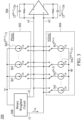
- FIG. 3 shows an N-bit DAC 300 in accordance with an exemplary embodiment of the present invention, which has a PDAC 302, an NDAC 304, a TIA 306, and a binary weighted circuit 308.
- the number of p-type current sources is 2 (N-1) -1 (referring to Ip1 ⁇ Ip(2 (N1) -1)).
- the number of n-type current sources is 2 (N-1) (referring to In1 ⁇ In2 (N-1) ).
- the fixed current is 1x.
- the 2 (N-1) -1 p-type current sources Ip1 ⁇ Ip(2 (N-1) -1) are all connected to the first input terminal n1 of the TIA 306, and the 2 (N-1) n-type current sources In1 ⁇ In2 (N-1) are all connected to the second input terminal n2 of the TIA 306.
- the current from the first node n1 to the output port of the TIA 306 is (2 (N-1) -1) ⁇ 1x.
- the current from the output port of the TIA 306 to the second node n2 is (2 (N-1) -1) ⁇ 1x.
- the 2 (N-1) -1 p-type current sources Ip1 ⁇ Ip(2 (N-1) -1) are all connected to the second input terminal n2 of the TIA 306, and the 2 (N-1) n-type current sources In1 ⁇ In2 (N-1) are all connected to the first input terminal n1 of the TIA 306.
Landscapes
- Engineering & Computer Science (AREA)
- Theoretical Computer Science (AREA)
- Analogue/Digital Conversion (AREA)
Abstract
Description
- The present invention relates to digital-to-analog converters (DACs), and, in particular, to a current-steering DAC.
- Technological progress (e.g., from WiFi 5 to WiFi 8) makes Error vector magnitude (EVM) requirements to be increased and Radio frequency (RF) impediments to be more obvious, meaning that digital calibration is more necessary. There is a trade-off between the DAC set point and DAC noise.
- A low-noise DAC with a small circuit size and high power performance is called for.
- A complementary current-steering digital-to-analog converter (DAC) is introduced.
- A complementary current-steering DAC in accordance with an exemplary embodiment of the present invention includes a transimpedance amplifier (TIA), a p-type DAC, and an n-type DAC. The p-type DAC has a plurality of p-type current sources. The p-type current sources are coupled to a first input terminal or a second input terminal of the TIA according to the digital input of the complementary current-steering DAC. The n-type DAC has a plurality of n-type current sources. The n-type current sources are coupled to the first input terminal or the second input terminal of the TIA according to the digital input of the complementary current-steering DAC. In response to the digital input changing from a first value to a second value that is greater than the first value, one or more n-type current sources connected to the second input terminal of the TIA are switched so that they are connected to the first input terminal of the TIA.
- In an exemplary embodiment, in response to the digital input changing from a third value to a fourth value that is greater than the third value, one or more p-type current sources connected to the first input terminal of the TIA are switched so that they are connected to the second input terminal of the TIA.
- In an exemplary embodiment, in response to the digital input changing from a fifth value to a sixth value that is greater than the fifth value, one or more p-type current sources connected to the first input terminal of the TIA are switched so that they are connected to the second input terminal of the TIA, and one or more of the n-type current sources connected to the second input terminal of the TIA are switched so that they are connected to the first input terminal of the TIA.
- In an exemplary embodiment, the digital input is N bits, wherein N is a number. The number of p-type current sources is 2(N-1)-1. The number of n-type current sources is 2(N-1).
- In an exemplary embodiment, in response to the digital input of 0, the 2(N-1)-1 p-type current sources are connected to the first input terminal of the TIA, and the 2(N-1) n-type current sources are connected to the second input terminal of the TIA.
- In an exemplary embodiment, in response to the digital input that is N bits of 1, the 2(N-1)-1 p-type current sources are connected to the second input terminal of the TIA, and the 2(N-1) n-type current sources are connected to the first input terminal of the TIA.
- In an exemplary embodiment, from 1 to 2(N-2), the greater the digital input is, the more n-type current sources are connected to the first input terminal of the TIA, and the 2(N-1)-1 p-type current sources are kept connected to the first input terminal of the TIA.
- In an exemplary embodiment, from 2(N-2)+1 to 2(N-2)+2(N1)-1, the greater the digital input is, the more p-type current sources are connected to the second input terminal of the TIA, and 2(N-2) n-type current sources are kept connected to the first input terminal of the TIA.
- In an exemplary embodiment, from 2(N-2)+2(N-1) to 2N-1, the greater the digital input is, the more n-type current sources are connected to the first input terminal of the TIA, and the 2(N-1)-1 p-type current sources are kept connected to the second input terminal of the TIA.
- In an exemplary embodiment, the complementary current-steering DAC further has a binary weighted circuit coupled to the second input terminal of the TIA to provide a fixed current. In an exemplary embodiment, the p-type current sources each output the fixed current, and the n-type current sources each output the fixed current.
- A detailed description is given in the following embodiments with reference to the accompanying drawings.
- The present invention can be more fully understood by reading the subsequent detailed description and examples with references made to the accompanying drawings, wherein:
-
FIG. 1 illustrates a complementary current-steering digital-to-analog converter (DAC) 100 in accordance with an exemplary embodiment of the present invention; -
FIGs 2A to 2H show how a 3-bit DAC 200 works in accordance with an exemplary embodiment of the present invention; and -
FIG. 3 shows an N-bit DAC 300 in accordance with an exemplary embodiment of the present invention. - The following description is made for the purpose of illustrating the general principles of the invention and should not be taken in a limiting sense. The scope of the invention is best determined by reference to the appended claims.
-
FIG. 1 illustrates a complementary current-steering digital-to-analog converter (DAC) 100 in accordance with an exemplary embodiment of the present invention. The complementary current-steering DAC 100 has a transimpedance amplifier (abbreviated as TIA) 102, a p-type digital-to-analog converter (abbreviated as PDAC) 104, and an n-type digital-to-analog converter (abbreviated as NDAC) 106. The TIA 102 may be known as a low-pass filter. - The PDAC 104 has a plurality of p-type current sources (e.g., implemented by PMOSs). The p-type current sources are coupled to a first input terminal n1 or a second input terminal n2 of the
TIA 102 according to the digital input IN of the complementary current-steering DAC 100. - The NDAC 106 has a plurality of n-type current sources (e.g., implemented by NMOSs). The n-type current sources are coupled to the first input terminal n1 or the second input terminal n2 of the
TIA 102 according to the digital input IN of the complementary current-steering DAC 100. - After the current-steering digital-to-analog conversion, an analog output is represented by the difference between VOP and VON.
- Different from a conventional current-steering DAC whose TIA has a first input terminal (n1) constantly connected to a n-type current source and a second input terminal (n2) constantly connected to another n-type current source, the
NDAC 106 form the complementary current-steering structure with thePDAC 104. With the flexibility of the bias current, the fewer current sources are required and the circuit size is considerably reduced. -
FIGs 2A to 2H show how a 3-bit DAC 200 works in accordance with an exemplary embodiment of the present invention. - The 3-
bit DAC 200 has three (2(3-1)-1) p-type current sources Ip1, Ip2 and Ip3 in thePDAC 202, and has four (2(3-1)) n-type current sources In1, In2, In3, and In4 in theNDAC 204. Switches are provided within thePDAC 202 and NDAC 204 to determine how to connect the p-type current sources Ip1∼Ip3 and the n-type current sources In1∼In4 to the first input terminal n1 or the second input terminal n2 of theTIA 206 according to the digital input IN of the 3-bit DAC 200. By controlling thePDAC 202 and NDAC 204 to change the bias current according to the digital input IN, an analog signal depending on the digital input IN is generated as the voltage difference at the output port of the TIA 206. The 3-bit DAC 200 further has a binary weightedcircuit 208, which has a first output terminal t1 coupled to the second input terminal n2 of the TIA 206, and a second output terminal t2 coupled to the first input terminal n1 of the TIA 206. The binaryweighted circuit 208 uses the first output terminal t1 to output a fixed current (64x, multiple of abase current 1x). Furthermore, the p-type current sources each output the fixed current (64x), and the n-type current sources each output the fixed current (64x). - In
FIG. 2A , the digital input IN is 3b' 000. The p-type current sources Ip1∼Ip3 are all connected to the first input terminal n1 of theTIA 206, and the n-type current sources In1∼In4 are all connected to the second input terminal n2 of theTIA 206. The current from the first node n1 to the output port of the TIA 206 is (64x)∗3. The current from the output port of the TIA 206 to the second node n2 is (64x)∗4 - 64x. - In
FIG. 2B , the digital input IN is 3b' 001. The p-type current sources Ip1∼Ip3 are all connected to the first input terminal n1 of the TIA 206, the n-type current source In1 is connected to the first input terminal n1 of theTIA 206, and the n-type current sources In2~In4 are connected to the second input terminal n2 of the TIA 206. The current from the first node n1 to the output port of the TIA 206 is (64x)∗2. The current from the output port of the TIA 206 to the second node n2 is (64x)∗3 - 64x. - In
FIG. 2C , the digital input IN is 3b' 010. The p-type current sources Ip1∼Ip3 are all connected to the first input terminal n1 of theTIA 206, the n-type current sources In1 and In2 are connected to the first input terminal n1 of theTIA 206, and the n-type current sources In3 and In4 are connected to the second input terminal n2 of the TIA 206. The current from the first node n1 to the output port of theTIA 206 is (64x)∗1. The current from the output port of theTIA 206 to the second node n2 is (64x)∗2 - 64x. - In
FIG. 2D , the digital input IN is 3b' 011. The p-type current source Ip1 is connected to the second input terminal n2 of theTIA 206, the p-type current sources Ip2 and Ip3 are connected to the first input terminal n1 of theTIA 206, the n-type current sources In1 and In2 are connected to the first input terminal n1 of theTIA 206, and the n-type current sources In3 and In4 are connected to the second input terminal n2 of theTIA 206. The current from the first node n1 to the output port of theTIA 206 is (64x)∗0. The current from the output port of theTIA 206 to the second node n2 is (64x)∗1 - 64x. - In
FIG. 2E , the digital input IN is 3b' 100. The p-type current sources Ip1 and Ip2 are connected to the second input terminal n2 of theTIA 206, the p-type current source Ip3 is connected to the first input terminal n1 of theTIA 206, the n-type current sources In1 and In2 are connected to the first input terminal n1 of theTIA 206, and the n-type current sources In3 and In4 are connected to the second input terminal n2 of theTIA 206. The current direction is changed in comparison withFIGs 2A-2D . The current from the output port of theTIA 206 to the first node n1 is (64x)∗1. The current from the second node n2 to the output port of theTIA 206 to is (64x)∗0 + 64x. - In
FIG. 2F , the digital input IN is 3b' 101. The p-type current sources Ip1 ∼ Ip3 are all connected to the second input terminal n2 of theTIA 206, the n-type current sources In1 and In2 are connected to the first input terminal n1 of theTIA 206, and the n-type current sources In3 and In4 are connected to the second input terminal n2 of theTIA 206. The current from the output port of theTIA 206 to the first node n1 is (64x)∗2. The current from the second node n2 to the output port of theTIA 206 to is (64x)∗1 + 64x. - In
FIG. 2G , the digital input IN is 3b' 110. The p-type current sources Ip1∼ Ip3 are all connected to the second input terminal n2 of theTIA 206, the n-type current sources In1∼In3 are connected to the first input terminal n1 of theTIA 206, and the n-type current source In4 is connected to the second input terminal n2 of theTIA 206. The current from the output port of theTIA 206 to the first node n1 is (64x)∗3. The current from the second node n2 to the output port of theTIA 206 to is (64x)∗2 + 64x. - In
FIG. 2H , the digital input IN is 3b' 111. The p-type current sources Ip1∼ Ip3 are all connected to the second input terminal n2 of theTIA 206, and the n-type current sources In1∼In4 are all connected to the first input terminal n1 of theTIA 206. The current from the output port of theTIA 206 to the first node n1 is (64x)∗4. The current from the second node n2 to the output port of theTIA 206 to is (64x)∗3 + 64x. - The control principles of the p-type current sources Ip1∼Ip3 and the n-type current sources In1∼In4 can be summarized in the following.
- Referring to
FIGs 2A-2C , in response to the digital input IN changing from a first value (3b' 000 ofFIG. 2A ) to a second value (3b' 001 ofFIG. 2B , or 3b' 010 ofFIG. 2C ) that is greater than the first value (3b' 000), one or more n-type current sources connected to the second input terminal n2 of theTIA 206 are switched so that they are connected to the first input terminal n1 of theTIA 206. For example, when being changed fromFIG. 2A to FIG. 2B , only the connection of In1 is changed. When being changed fromFIG. 2A to FIG. 2C , both In1 and In2 are changed in their connections. The connection change fromFIG. 2B to FIG. 2C , or fromFIG. 2F to FIG. 2G , or fromFIG. 2F to FIG. 2H , or fromFIG. 2G to FIG. 2H follow the same principle. In these examples, the connection of the p-type current sources Ip1∼Ip3 are kept. - Referring to
FIGs 2C-2F , in response to the digital input IN changing from a third value (3b' 010 ofFIG. 2C ) to a fourth value (3b' 011 ofFIG. 2D , or 3b' 100 ofFIG. 2E , or 3b' 101 ofFIG. 2F ) that is greater than the third value (3b' 010), one or more p-type current sources connected to the first input terminal n1 of theTIA 206 are switched so that they are connected to the second input terminal n2 of theTIA 206. For example, when being changed fromFIG. 2C to FIG. 2D , only the connection of Ip1 is changed. When being changed fromFIG. 2C to FIG. 2E , both Ip1 and Ip2 are changed in their connections. When being changed fromFIG. 2C to FIG. 2F , Ip1∼Ip3 are all changed in their connections. The connection change fromFIG. 2D to FIG. 2E , or fromFIG. 2D to FIG. 2F , or fromFIG. 2E to FIG. 2F follow the same principle. - Referring to
FIGs 2A ,2G , and2H , in response to the digital input IN changing from a fifth value (3b' 000 ofFIG. 2A ) to a sixth value (3b' 110 ofFIG. 2G , or 3b' 111 ofFIG. 2H ) that is greater than the fifth value (3b' 000), one or more p-type current sources connected to the first input terminal n1 of theTIA 206 are switched so that they are connected to the second input terminal n2 of theTIA 206, and one or more of the n-type current sources connected to the second input terminal n2 of theTIA 206 are switched so that they are connected to the first input terminal n1 of theTIA 206. For example, when being changed fromFIG. 2A to FIG. 2G , the connections of Ip1∼Ip3 and In1∼In3 are changed. When being changed fromFIG. 2A to FIG. 2H , the connections of Ip1∼Ip3 and In1∼In4 are all changed. - In another perspective, the control principles of the p-type current sources Ip1∼Ip3 and the n-type current sources In1∼In4 are summarized in the following.
- In response to the digital input IN changing from the second value (3b' 010 of
FIG. 2C ) to the seventh value (3b' 011 ofFIG. 2D , or 3b' 100 ofFIG. 2E , or 3b' 101 ofFIG. 2F ) that is greater than the second value (3b' 010), one or more of the p-type current sources connected to the first input terminal n1 of theTIA 206 are switched so that they are connected to the second input terminal n2 of theTIA 206, and the connection of the n-type current sources In1∼In4 are kept. - In response to the digital input IN changing from the seventh value (3b' 011 of
FIG. 2D ) to an eighth value (3b' 100 ofFIG. 2E , or 3b' 101 ofFIG. 2F ) that is greater than theseventh value 3b' 011, one or more of the p-type current sources connected to the first input terminal n1 of theTIA 206 are switched so that they are connected to the second input terminal n2 of theTIA 206, and the connection of the n-type current sources In1∼In4 are kept. - In response to the digital input IN changing from the eighth value (3b' 101 of
FIG. 2F ) to a ninth value (3b' 110 ofFIG. 2G , or 3b' 111 ofFIG. 2H ) that is greater than the eighth value (3b' 101), one or more of the n-type current sources connected to the second input terminal n2 of theTIA 206 are switched so that they are connected to the first input terminal n1 of theTIA 206, and the connection of the p-type current sources Ip1∼Ip3 are kept. - In response to the digital input IN changing from the ninth value (3b' 110 of
FIG. 2G ) to a tenth value (3b' 111 ofFIG. 2H ) that is greater than the ninth value (3b' 110), one or more of the n-type current sources connected to the second input terminal n2 of theTIA 206 are switched so that they are connected to the first input terminal n1 of theTIA 206, and the connection of the p-type current sources Ip1∼Ip3 are kept. -
FIG. 3 shows an N-bit DAC 300 in accordance with an exemplary embodiment of the present invention, which has aPDAC 302, anNDAC 304, aTIA 306, and a binaryweighted circuit 308. In thePDAC 302, the number of p-type current sources is 2(N-1)-1 (referring to Ip1∼Ip(2(N1)-1)). In theNDAC 304, the number of n-type current sources is 2(N-1) (referring to In1∼In2(N-1)). The fixed current is 1x. - In response to the digital input IN of 0, the 2(N-1)-1 p-type current sources Ip1∼Ip(2(N-1)-1) are all connected to the first input terminal n1 of the
TIA 306, and the 2(N-1) n-type current sources In1∼In2(N-1) are all connected to the second input terminal n2 of theTIA 306. The current from the first node n1 to the output port of theTIA 306 is (2(N-1)-1)∗1x. The current from the output port of theTIA 306 to the second node n2 is (2(N-1)-1)∗1x. - In response to the digital input IN that is N bits of 1, the 2(N-1)-1 p-type current sources Ip1∼Ip(2(N-1)-1) are all connected to the second input terminal n2 of the
TIA 306, and the 2(N-1) n-type current sources In1∼In2(N-1) are all connected to the first input terminal n1 of theTIA 306. - From 1 to 2(N-2), the greater the digital input IN is, the more n-type current sources are connected to the first input terminal n1 of the
TIA 306, and the 2(N-1)-1 p-type current sources Ip1∼Ip(2(N-1)-1) are kept connected to the first input terminal n1 of theTIA 306. - From 2(N-2)+1 to 2(N-2)+2(N-1)-1, the greater the digital input IN is, the more p-type current sources are connected to the second input terminal n2 of the
TIA 306, and the 2(N-2) n-type current sources In1∼In2(N-2) are kept connected to the first input terminal n1 of theTIA 306. - From 2(N-2)+2(N-1) to 2N-1, the greater the digital input IN is, the more n-type current sources are connected to the first input terminal n1 of the
TIA 306, and the 2(N-1)-1 p-type current sources Ip1∼Ip(2(N-1)-1) are kept connected to the second input terminal n2 of theTIA 306. - Any current-steering DAC with the aforementioned complementary bias design (PDAC and NDAC) should be considered within the scope of the present invention.
- While the invention has been described by way of example and in terms of the preferred embodiments, it should be understood that the invention is not limited to the disclosed embodiments. On the contrary, it is intended to cover various modifications and similar arrangements (as would be apparent to those skilled in the art). Therefore, the scope of the appended claims should be accorded the broadest interpretation so as to encompass all such modifications and similar arrangements.
Claims (15)
- A complementary current-steering digital-to-analog converter, comprising:a transimpedance amplifier;a p-type digital-to-analog converter, comprising a plurality of p-type current sources, wherein the p-type current sources are coupled to a first input terminal or a second input terminal of the transimpedance amplifier according to a digital input of the complementary current-steering digital-to-analog converter; andan n-type digital-to-analog converter, comprising a plurality of n-type current sources, wherein the n-type current sources are coupled to the first input terminal or the second input terminal of the transimpedance amplifier according to the digital input of the complementary current-steering digital-to-analog converter;wherein:
in response to the digital input changing from a first value to a second value that is greater than the first value, one or more n-type current sources connected to the second input terminal of the transimpedance amplifier are switched so that they are connected to the first input terminal of the transimpedance amplifier. - The complementary current-steering digital-to-analog converter as claimed in claim 1, wherein:
in response to the digital input changing from a third value to a fourth value that is greater than the third value, one or more p-type current sources connected to the first input terminal of the transimpedance amplifier are switched so that they are connected to the second input terminal of the transimpedance amplifier. - The complementary current-steering digital-to-analog converter as claimed in claim 1 or 2, wherein:
in response to the digital input changing from a fifth value to a sixth value that is greater than the fifth value, one or more p-type current sources connected to the first input terminal of the transimpedance amplifier are switched so that they are connected to the second input terminal of the transimpedance amplifier, and one or more n-type current sources connected to the second input terminal of the transimpedance amplifier are switched so that they are connected to the first input terminal of the transimpedance amplifier. - The complementary current-steering digital-to-analog converter as claimed in any one of the preceding claims, wherein:
in response to the digital input changing from the first value to the second value, the connection of the p-type current sources are kept. - The complementary current-steering digital-to-analog converter as claimed in claim 4, wherein:
in response to the digital input changing from the second value to a seventh value that is greater than the second value, one or more p-type current sources connected to the first input terminal of the transimpedance amplifier are switched so that they are connected to the second input terminal of the transimpedance amplifier, and the connection of the n-type current sources are kept. - The complementary current-steering digital-to-analog converter as claimed in claim 5, wherein:
in response to the digital input changing from the seventh value to an eighth value that is greater than the seventh value, one or more of the p-type current sources connected to the first input terminal of the transimpedance amplifier are switched so that they are connected to the second input terminal of the transimpedance amplifier, and the connection of the n-type current sources are kept. - The complementary current-steering digital-to-analog converter as claimed in claim 6, wherein:
in response to the digital input changing from the eighth value to a ninth value that is greater than the eighth value, one or more of the n-type current sources connected to the second input terminal of the transimpedance amplifier are switched so that they are connected to the first input terminal of the transimpedance amplifier, and the connection of the p-type current sources are kept. - The complementary current-steering digital-to-analog converter as claimed in claim 7, wherein:
in response to the digital input changing from the ninth value to a tenth value that is greater than the ninth value, one or more of the n-type current sources connected to the second input terminal of the transimpedance amplifier are switched so that they are connected to the first input terminal of the transimpedance amplifier, and the connection of the p-type current sources are kept. - The complementary current-steering digital-to-analog converter as claimed in any one of the preceding claims, wherein:the digital input is N bits, wherein N is a number;the number of p-type current sources is 2(N-1)-1; andthe number of n-type current sources is 2(N-1).
- The complementary current-steering digital-to-analog converter as claimed in claim 9, wherein:
in response to the digital input of 0, the 2(N-1)-1 p-type current sources are connected to the first input terminal of the transimpedance amplifier, and the 2(N-1) n-type current sources are connected to the second input terminal of the transimpedance amplifier. - The complementary current-steering digital-to-analog converter as claimed in claim 10, wherein:
in response to the digital input that is N bits of 1, the 2(N-1)-1 p-type current sources are connected to the second input terminal of the transimpedance amplifier, and the 2(N-1) n-type current sources are connected to the first input terminal of the transimpedance amplifier. - The complementary current-steering digital-to-analog converter as claimed in claim 11, wherein:
from 1 to 2(N-2), the greater the digital input is, the more n-type current sources are connected to the first input terminal of the transimpedance amplifier, and the 2(N-1)-1 p-type current sources are kept connected to the first input terminal of the transimpedance amplifier. - The complementary current-steering digital-to-analog converter as claimed in claim 12, wherein:
from 2(N-2)+1 to 2(N-2)+2(N-1)-1, the greater the digital input is, the more p-type current sources are connected to the second input terminal of the transimpedance amplifier, and 2(N-2) n-type current sources are kept connected to the first input terminal of the transimpedance amplifier. - The complementary current-steering digital-to-analog converter as claimed in claim 13, wherein:
from 2(N-2)+2(N-1) to 2N-1, the greater the digital input is, the more n-type current sources are connected to the first input terminal of the transimpedance amplifier, and the 2(N-1)-1 p-type current sources are kept connected to the second input terminal of the transimpedance amplifier. - The complementary current-steering digital-to-analog converter as claimed in any one of the preceding claims, further comprising:a binary weighted circuit, having a first output terminal coupled to the second input terminal of the transimpedance amplifier, and a second output terminal coupled to the first input terminal of the transimpedance amplifier, wherein the binary weighted circuit uses the first output terminal to output a fixed current;wherein it is preferred that:the p-type current sources each output the fixed current; andthe n-type current sources each output the fixed current.
Applications Claiming Priority (2)
| Application Number | Priority Date | Filing Date | Title |
|---|---|---|---|
| US202263370398P | 2022-08-04 | 2022-08-04 | |
| US18/325,035 US12355467B2 (en) | 2022-08-04 | 2023-05-29 | Complementary current-steering digital-to-analog converter |
Publications (1)
| Publication Number | Publication Date |
|---|---|
| EP4318953A1 true EP4318953A1 (en) | 2024-02-07 |
Family
ID=87158105
Family Applications (1)
| Application Number | Title | Priority Date | Filing Date |
|---|---|---|---|
| EP23183733.7A Pending EP4318953A1 (en) | 2022-08-04 | 2023-07-05 | Complementary current-steering digital-to-analog converter |
Country Status (2)
| Country | Link |
|---|---|
| US (1) | US12355467B2 (en) |
| EP (1) | EP4318953A1 (en) |
Citations (3)
| Publication number | Priority date | Publication date | Assignee | Title |
|---|---|---|---|---|
| JPH09238078A (en) * | 1996-01-26 | 1997-09-09 | Texas Instr Inc <Ti> | D/a converter |
| US9065463B2 (en) * | 2013-10-11 | 2015-06-23 | Analog Devices Global | Method and apparatus for reducing capacitor induced ISI in DACS |
| US10693489B2 (en) * | 2018-01-22 | 2020-06-23 | Samsung Electronics Co., Ltd. | Circuit and method for digital-to-analog conversion using three-level cells |
Family Cites Families (44)
| Publication number | Priority date | Publication date | Assignee | Title |
|---|---|---|---|---|
| SE518113C2 (en) * | 2000-03-06 | 2002-08-27 | Ericsson Telefon Ab L M | Method and apparatus for improving current-controlled D / A conversion |
| DE10038372C2 (en) * | 2000-08-07 | 2003-03-13 | Infineon Technologies Ag | Differential digital / analog converter |
| TW463466B (en) * | 2000-08-30 | 2001-11-11 | Silicon Integrated Sys Corp | Current A/D converter and the unit cell thereof |
| US6809673B2 (en) * | 2001-10-10 | 2004-10-26 | Analog Devices, Inc. | Multi-channel circuit with current steering digital to analogue converters with minimized crosstalk |
| US6741195B1 (en) * | 2002-12-11 | 2004-05-25 | Micron Technology, Inc. | Low glitch current steering digital to analog converter and method |
| US7019677B1 (en) * | 2004-09-08 | 2006-03-28 | Cirrus Logic, Inc. | Current steering digital to analog converters with self-calibration, and systems and methods using the same |
| US6967609B1 (en) * | 2004-11-12 | 2005-11-22 | Lsi Logic Corporation | Method and apparatus for dynamically biasing switching elements in current-steering DAC |
| US7023367B1 (en) * | 2005-03-10 | 2006-04-04 | National Semiconductor Corporation | Current steering digital to analog converter with improved dynamic linearity |
| JP4546539B2 (en) * | 2005-10-17 | 2010-09-15 | パナソニック株式会社 | Current addition type DAC |
| CN101501996B (en) * | 2006-08-07 | 2011-09-07 | 松下电器产业株式会社 | Multi-channel current summing DAC |
| US7348911B2 (en) * | 2006-08-08 | 2008-03-25 | Atmel Corporation | Common mode management between a current-steering DAC and transconductance filter in a transmission system |
| US7629910B2 (en) * | 2006-08-30 | 2009-12-08 | Texas Instruments Incorporated | Methods and apparatus to control current steering digital to analog converters |
| US7388531B1 (en) * | 2006-09-26 | 2008-06-17 | Marvell International Ltd. | Current steering DAC using thin oxide devices |
| US7557743B2 (en) * | 2006-12-08 | 2009-07-07 | Kabushiki Kaisha Toshiba | D/A converter |
| US7561979B2 (en) * | 2007-05-10 | 2009-07-14 | Mediatek Inc. | Device and method for calibrating data processing apparatus by tuning firmware trim value |
| EP2026467B1 (en) * | 2007-07-30 | 2011-07-13 | ST-Ericsson SA | Current steering digital-analog converter particularly insensitive to packaging stresses |
| TWI354449B (en) * | 2008-02-12 | 2011-12-11 | Faraday Tech Corp | Current steering dac and voltage booster for curre |
| US7576675B1 (en) * | 2008-03-25 | 2009-08-18 | Megawin Technology Co., Ltd. | Return-to-zero current-steering DAC with clock-to-output isolation |
| US7847717B2 (en) * | 2009-04-01 | 2010-12-07 | Texas Instruments Incorporated | Low noise current steering DAC |
| TWI454062B (en) * | 2009-05-15 | 2014-09-21 | Realtek Semiconductor Corp | Self-calibrated current source and dac using the same and operation method thereof |
| US7969340B2 (en) * | 2009-07-22 | 2011-06-28 | Mediatek Inc. | Noise-shaped segmented digital-to-analog converter |
| US8009074B2 (en) * | 2010-01-12 | 2011-08-30 | Mediatek Inc. | Digital-to-analog converter and code mapping method applied to the digital-to-analog converter |
| US8441382B2 (en) * | 2010-03-15 | 2013-05-14 | Stmicroelectronics Pvt. Ltd. | Current steering DAC with switched cascode output current source/sink |
| US8237497B2 (en) * | 2010-04-06 | 2012-08-07 | Mediatek Inc. | Amplifier for processing differential input using amplifier circuits with different driving capabilities and/or different frequency compensation characteristics |
| US8451150B2 (en) * | 2010-04-11 | 2013-05-28 | Mediatek Inc. | Transceiver and method for converting signals of the transceiver thereof |
| US8344922B2 (en) * | 2010-08-03 | 2013-01-01 | Crest Semiconductors, Inc. | Digital-to-analog converter with code independent output capacitance |
| US8456341B2 (en) * | 2011-06-03 | 2013-06-04 | Texas Instruments Incorporated | Three-level digital-to-analog converter |
| US8525586B2 (en) * | 2011-08-15 | 2013-09-03 | Mediatek Inc. | Gain stage with DC offset compensation and method thereof |
| US8653999B1 (en) * | 2012-09-05 | 2014-02-18 | Nxp B.V. | Current steering DAC, a video adapter including a current steering DAC, and a video circuit including a current steering DAC |
| US8842032B2 (en) * | 2012-11-30 | 2014-09-23 | Analog Devices, Inc. | Enhanced second order noise shaped segmentation and dynamic element matching technique |
| US9350372B2 (en) * | 2012-12-06 | 2016-05-24 | Taiwan Semiconductor Manufacturing Company Limited | Arrangement for digital-to-analog converter |
| US9148160B2 (en) * | 2013-08-14 | 2015-09-29 | Maxlinear, Inc. | Dynamic power switching in current-steering DACs |
| US9130587B2 (en) * | 2014-01-29 | 2015-09-08 | Broadcom Corporation | Frame adaptive digital to analog converter and methods for use therewith |
| US9112528B1 (en) * | 2014-01-29 | 2015-08-18 | Broadcom Corporation | Digital to analog converter with thermometer coding and methods for use therewith |
| US9136864B1 (en) * | 2014-02-26 | 2015-09-15 | Maxim Integrated Products, Inc. | Method for trimming segment currents in current steering DAC based on most back gate voltage modulation |
| US9231607B2 (en) * | 2014-02-26 | 2016-01-05 | Maxim Integrated Products, Inc. | Interconnect structures for minimizing clock and output timing skews in a high speed current steering DAC |
| US9509326B1 (en) * | 2015-06-10 | 2016-11-29 | Intel IP Corporation | Apparatus for correcting linearity of a digital-to-analog converter |
| US9991900B1 (en) * | 2017-08-02 | 2018-06-05 | Nxp Usa, Inc. | Digital to analog (DAC) converter with current calibration |
| US10069505B1 (en) * | 2017-09-13 | 2018-09-04 | Keysight Technologies, Inc. | Least significant bit dynamic element matching in a digital-to-analog converter |
| US10797720B2 (en) * | 2018-09-21 | 2020-10-06 | Qualcomm Incorporated | Apparatus and method for measuring current source mismatches in current-steering DAC by re-using R2R network |
| US10425099B1 (en) * | 2018-11-29 | 2019-09-24 | Ciena Corporation | Extremely-fine resolution sub-ranging current mode Digital-Analog-Converter using Sigma-Delta modulators |
| US11711090B2 (en) * | 2019-11-27 | 2023-07-25 | Vervesemi Microelectronics Private Limited | Current steering digital to analog converter (DAC) system to perform DAC static linearity calibration |
| US11043959B1 (en) * | 2019-12-06 | 2021-06-22 | Cirrus Logic, Inc. | Current digital-to-analog converter with warming of digital-to-analog converter elements |
| US11362668B1 (en) * | 2021-04-07 | 2022-06-14 | Infineon Technologies Ag | Leakage compensation for analog decoded thermometric digital-to-analog converter (DAC) |
-
2023
- 2023-05-29 US US18/325,035 patent/US12355467B2/en active Active
- 2023-07-05 EP EP23183733.7A patent/EP4318953A1/en active Pending
Patent Citations (3)
| Publication number | Priority date | Publication date | Assignee | Title |
|---|---|---|---|---|
| JPH09238078A (en) * | 1996-01-26 | 1997-09-09 | Texas Instr Inc <Ti> | D/a converter |
| US9065463B2 (en) * | 2013-10-11 | 2015-06-23 | Analog Devices Global | Method and apparatus for reducing capacitor induced ISI in DACS |
| US10693489B2 (en) * | 2018-01-22 | 2020-06-23 | Samsung Electronics Co., Ltd. | Circuit and method for digital-to-analog conversion using three-level cells |
Non-Patent Citations (1)
| Title |
|---|
| DE WIT P ET AL: "Complementary DAC topology for reduced output impedance dependency and improved dynamic performance", ELECTRONICS LETTERS, THE INSTITUTION OF ENGINEERING AND TECHNOLOGY, GB, vol. 48, no. 17, 16 August 2012 (2012-08-16), pages 1039 - 1041, XP006041138, ISSN: 0013-5194, DOI: 10.1049/EL.2012.1142 * |
Also Published As
| Publication number | Publication date |
|---|---|
| US12355467B2 (en) | 2025-07-08 |
| US20240048149A1 (en) | 2024-02-08 |
Similar Documents
| Publication | Publication Date | Title |
|---|---|---|
| CN101888248B (en) | Digital-to-analog converter | |
| US7068201B1 (en) | Digital-to-analog converter | |
| US5790060A (en) | Digital-to-analog converter having enhanced current steering and associated method | |
| US8493257B2 (en) | Current-switching cell and digital-to-analog converter | |
| US6977602B1 (en) | Wide band digital to analog converters and methods, including converters with selectable impulse response | |
| US5446455A (en) | Auto-calibrated current-mode digital-to-analog converter and method therefor | |
| US9094042B2 (en) | DAC current source matrix patterns with gradient error cancellation | |
| EP2156561A1 (en) | Pseudo-differential class-ab digital-to-analog converter with code dependent dc current | |
| CN106341134B (en) | Digital-to-analog converter with local interleaving and resampling | |
| US7030799B2 (en) | Current-steering digital-to-analog converter | |
| KR100384787B1 (en) | Digital-Analog Converter | |
| KR20000053011A (en) | A method and device to provide a high-performance digital-to-analog conversion architecture | |
| US9143156B1 (en) | High-resolution digital to analog converter | |
| JP3528958B2 (en) | Current addition type DA converter | |
| US12355467B2 (en) | Complementary current-steering digital-to-analog converter | |
| US9584152B1 (en) | Current steering digital to analog converter with dual current switch modules | |
| US20250337422A1 (en) | Complementary current-steering digital-to-analog converter | |
| Liu et al. | An 8-bit 10 MS/s folding and interpolating ADC using the continuous-time auto-zero technique | |
| US7403149B2 (en) | Folding and interpolating analog-to-digital converter and method of converting analog signal to digital signal | |
| CN117526950A (en) | Complementary Current Steering Digital-to-Analog Converter | |
| US11070219B2 (en) | Digital/analog converter | |
| US11750205B1 (en) | Current digital-to-analog converter with distributed reconstruction filtering | |
| US11728824B2 (en) | Analog circuit and comparator sharing method of analog circuit | |
| US20040041721A1 (en) | High-speed low-distortion analog-to digital converter | |
| KR20140128573A (en) | Split Hierarchical Symmetrical Switching Scheme of Digital Analog Convert for Static Linearity Improvement and Apparatus Therefor |
Legal Events
| Date | Code | Title | Description |
|---|---|---|---|
| PUAI | Public reference made under article 153(3) epc to a published international application that has entered the european phase |
Free format text: ORIGINAL CODE: 0009012 |
|
| STAA | Information on the status of an ep patent application or granted ep patent |
Free format text: STATUS: THE APPLICATION HAS BEEN PUBLISHED |
|
| AK | Designated contracting states |
Kind code of ref document: A1 Designated state(s): AL AT BE BG CH CY CZ DE DK EE ES FI FR GB GR HR HU IE IS IT LI LT LU LV MC ME MK MT NL NO PL PT RO RS SE SI SK SM TR |
|
| STAA | Information on the status of an ep patent application or granted ep patent |
Free format text: STATUS: REQUEST FOR EXAMINATION WAS MADE |
|
| 17P | Request for examination filed |
Effective date: 20240807 |
|
| RBV | Designated contracting states (corrected) |
Designated state(s): AL AT BE BG CH CY CZ DE DK EE ES FI FR GB GR HR HU IE IS IT LI LT LU LV MC ME MK MT NL NO PL PT RO RS SE SI SK SM TR |
|
| STAA | Information on the status of an ep patent application or granted ep patent |
Free format text: STATUS: EXAMINATION IS IN PROGRESS |
|
| 17Q | First examination report despatched |
Effective date: 20251110 |