EP4318565A1 - Semiconductor device and phase characteristic adjustment method therefor - Google Patents
Semiconductor device and phase characteristic adjustment method therefor Download PDFInfo
- Publication number
- EP4318565A1 EP4318565A1 EP22775118.7A EP22775118A EP4318565A1 EP 4318565 A1 EP4318565 A1 EP 4318565A1 EP 22775118 A EP22775118 A EP 22775118A EP 4318565 A1 EP4318565 A1 EP 4318565A1
- Authority
- EP
- European Patent Office
- Prior art keywords
- circuit board
- semiconductor device
- base
- wire
- wires
- Prior art date
- Legal status (The legal status is an assumption and is not a legal conclusion. Google has not performed a legal analysis and makes no representation as to the accuracy of the status listed.)
- Pending
Links
Images





Classifications
-
- H—ELECTRICITY
- H10—SEMICONDUCTOR DEVICES; ELECTRIC SOLID-STATE DEVICES NOT OTHERWISE PROVIDED FOR
- H10W—GENERIC PACKAGES, INTERCONNECTIONS, CONNECTORS OR OTHER CONSTRUCTIONAL DETAILS OF DEVICES COVERED BY CLASS H10
- H10W72/00—Interconnections or connectors in packages
- H10W72/50—Bond wires
-
- H—ELECTRICITY
- H01—ELECTRIC ELEMENTS
- H01P—WAVEGUIDES; RESONATORS, LINES, OR OTHER DEVICES OF THE WAVEGUIDE TYPE
- H01P1/00—Auxiliary devices
- H01P1/04—Fixed joints
- H01P1/047—Strip line joints
-
- H—ELECTRICITY
- H10—SEMICONDUCTOR DEVICES; ELECTRIC SOLID-STATE DEVICES NOT OTHERWISE PROVIDED FOR
- H10W—GENERIC PACKAGES, INTERCONNECTIONS, CONNECTORS OR OTHER CONSTRUCTIONAL DETAILS OF DEVICES COVERED BY CLASS H10
- H10W44/00—Electrical arrangements for controlling or matching impedance
- H10W44/20—Electrical arrangements for controlling or matching impedance at high-frequency [HF] or radio frequency [RF]
-
- H—ELECTRICITY
- H10—SEMICONDUCTOR DEVICES; ELECTRIC SOLID-STATE DEVICES NOT OTHERWISE PROVIDED FOR
- H10W—GENERIC PACKAGES, INTERCONNECTIONS, CONNECTORS OR OTHER CONSTRUCTIONAL DETAILS OF DEVICES COVERED BY CLASS H10
- H10W70/00—Package substrates; Interposers; Redistribution layers [RDL]
- H10W70/60—Insulating or insulated package substrates; Interposers; Redistribution layers
-
- H—ELECTRICITY
- H01—ELECTRIC ELEMENTS
- H01F—MAGNETS; INDUCTANCES; TRANSFORMERS; SELECTION OF MATERIALS FOR THEIR MAGNETIC PROPERTIES
- H01F3/00—Cores, Yokes, or armatures
- H01F3/08—Cores, Yokes, or armatures made from powder
-
- H—ELECTRICITY
- H10—SEMICONDUCTOR DEVICES; ELECTRIC SOLID-STATE DEVICES NOT OTHERWISE PROVIDED FOR
- H10W—GENERIC PACKAGES, INTERCONNECTIONS, CONNECTORS OR OTHER CONSTRUCTIONAL DETAILS OF DEVICES COVERED BY CLASS H10
- H10W44/00—Electrical arrangements for controlling or matching impedance
- H10W44/20—Electrical arrangements for controlling or matching impedance at high-frequency [HF] or radio frequency [RF]
- H10W44/203—Electrical connections
- H10W44/206—Wires
-
- H—ELECTRICITY
- H10—SEMICONDUCTOR DEVICES; ELECTRIC SOLID-STATE DEVICES NOT OTHERWISE PROVIDED FOR
- H10W—GENERIC PACKAGES, INTERCONNECTIONS, CONNECTORS OR OTHER CONSTRUCTIONAL DETAILS OF DEVICES COVERED BY CLASS H10
- H10W44/00—Electrical arrangements for controlling or matching impedance
- H10W44/20—Electrical arrangements for controlling or matching impedance at high-frequency [HF] or radio frequency [RF]
- H10W44/203—Electrical connections
- H10W44/216—Waveguides, e.g. strip lines
-
- H—ELECTRICITY
- H10—SEMICONDUCTOR DEVICES; ELECTRIC SOLID-STATE DEVICES NOT OTHERWISE PROVIDED FOR
- H10W—GENERIC PACKAGES, INTERCONNECTIONS, CONNECTORS OR OTHER CONSTRUCTIONAL DETAILS OF DEVICES COVERED BY CLASS H10
- H10W44/00—Electrical arrangements for controlling or matching impedance
- H10W44/20—Electrical arrangements for controlling or matching impedance at high-frequency [HF] or radio frequency [RF]
- H10W44/226—Electrical arrangements for controlling or matching impedance at high-frequency [HF] or radio frequency [RF] for HF amplifiers
- H10W44/234—Arrangements for impedance matching
-
- H—ELECTRICITY
- H10—SEMICONDUCTOR DEVICES; ELECTRIC SOLID-STATE DEVICES NOT OTHERWISE PROVIDED FOR
- H10W—GENERIC PACKAGES, INTERCONNECTIONS, CONNECTORS OR OTHER CONSTRUCTIONAL DETAILS OF DEVICES COVERED BY CLASS H10
- H10W72/00—Interconnections or connectors in packages
- H10W72/071—Connecting or disconnecting
- H10W72/075—Connecting or disconnecting of bond wires
- H10W72/07551—Connecting or disconnecting of bond wires characterised by changes in properties of the bond wires during the connecting
- H10W72/07552—Connecting or disconnecting of bond wires characterised by changes in properties of the bond wires during the connecting changes in structures or sizes
-
- H—ELECTRICITY
- H10—SEMICONDUCTOR DEVICES; ELECTRIC SOLID-STATE DEVICES NOT OTHERWISE PROVIDED FOR
- H10W—GENERIC PACKAGES, INTERCONNECTIONS, CONNECTORS OR OTHER CONSTRUCTIONAL DETAILS OF DEVICES COVERED BY CLASS H10
- H10W72/00—Interconnections or connectors in packages
- H10W72/50—Bond wires
- H10W72/521—Structures or relative sizes of bond wires
-
- H—ELECTRICITY
- H10—SEMICONDUCTOR DEVICES; ELECTRIC SOLID-STATE DEVICES NOT OTHERWISE PROVIDED FOR
- H10W—GENERIC PACKAGES, INTERCONNECTIONS, CONNECTORS OR OTHER CONSTRUCTIONAL DETAILS OF DEVICES COVERED BY CLASS H10
- H10W72/00—Interconnections or connectors in packages
- H10W72/50—Bond wires
- H10W72/541—Dispositions of bond wires
- H10W72/5445—Dispositions of bond wires being orthogonal to a side surface of the chip, e.g. parallel arrangements
-
- H—ELECTRICITY
- H10—SEMICONDUCTOR DEVICES; ELECTRIC SOLID-STATE DEVICES NOT OTHERWISE PROVIDED FOR
- H10W—GENERIC PACKAGES, INTERCONNECTIONS, CONNECTORS OR OTHER CONSTRUCTIONAL DETAILS OF DEVICES COVERED BY CLASS H10
- H10W90/00—Package configurations
- H10W90/701—Package configurations characterised by the relative positions of pads or connectors relative to package parts
- H10W90/751—Package configurations characterised by the relative positions of pads or connectors relative to package parts of bond wires
- H10W90/754—Package configurations characterised by the relative positions of pads or connectors relative to package parts of bond wires between a chip and a stacked insulating package substrate, interposer or RDL
Definitions
- Embodiments described herein relate generally to a semiconductor device and a method for adjusting phase characteristics thereof.
- a coupled-line conductor is formed on a surface of a semiconductor substrate.
- the semiconductor substrate has a storage hole for storing a ferrite sphere at a position away from a center portion.
- a ferrite single-crystal sphere in a magnetostatic mode is stored in the storage hole.
- a semiconductor device has a plurality of circuit boards therein, and each circuit board is connected by wires.
- it has become desirable to mount many devices on circuit boards to realize various functions. For this reason, it has become necessary to increase the size of the internal circuit boards in semiconductor devices.
- the size of the circuit board is increased, the distance between the circuit boards becomes narrower due to the limitation of the internal size of the semiconductor device, and, as a result, the length of the wires connecting the circuit boards also becomes shorter. If the wires become shorter, phase characteristics cannot be maintained, and the performance of the semiconductor device may deteriorate.
- the purpose of the embodiments is to provide, in a case where a plurality of circuit boards are arranged therein, a semiconductor device and a method for adjusting the phase characteristics thereof that can maintain the phase characteristics and prevent deterioration of the performance even if the wires connecting the circuit boards are shortened.
- a semiconductor device comprises a base, a first circuit board provided on the base, a second circuit board provided on the base at a certain interval from the first circuit board, a first connector provided with a first wire that is bridged between an upper surface of the first circuit board and an upper surface of the second circuit board to connect the two boards, and a first ferrite arranged on the base and directly below the first wire between the first circuit board and the second circuit board.
- a method for adjusting phase characteristics of a semiconductor device provides a first circuit board and a second circuit board at certain intervals on a base, bridges a first wire between an upper surface of the first circuit board and an upper surface of the second circuit board to connect the two boards, and arranges a first ferrite on the base and directly below the first wire between the first circuit board and the second circuit board to adjust phase characteristics of the first wire.
- FIG. 1 is a plan view showing a schematic configuration of a semiconductor device according to a first embodiment
- FIG. 2 is a cross-sectional view showing a cross-section of the semiconductor device shown in FIG. 1 along line A-A.
- a semiconductor device 1 comprises a base 10, one side of which is a mounting surface for electronic components and the other side of which is a heat dissipation surface.
- the upper surface of the base 10, i.e., the mounting surface for electronic components, is provided with a cover 11 formed into a box shape, for example, by a shielding material, so as to cover the entire surface.
- a first circuit board 12 and a second circuit board 13 of the same shape as the first circuit board 12 are placed at predetermined intervals.
- the first circuit board 12 and the second circuit board 13 are, for example, matching circuits that contain alumina (aluminum oxide: Al2O3) as a material and have a predetermined dielectric constant.
- an FET board 14 on which a field effect transistor (FFT) power amplification circuit is formed.
- the FET board 14 has a rectangular shape and is arranged in parallel between the first circuit board 12 and the second circuit board 13.
- a lead electrode part (first electrode part) 15 and a lead electrode part (second electrode part) 16 are provided so as to penetrate a part of a wall surface (top side and bottom side in FIG. 1 ) of the cover 11 that is in contact with the base 10.
- first wires configuring a first connector W1 are bridged between the upper surface of the first circuit board 12 and the upper surface of the FET board 14, and the boards are electrically connected by the first wires.
- One or more second wires configuring a second connector W2 are also bridged between the upper surface of the FET board 14 and the upper surface of the second circuit board 13, and the boards are electrically connected by the second wires. Both wires used for the first connector W1 and the second connector W2 are formed into an arch shape that, in the connected state, draws a semicircle on the upper side with respect to the base 10. Note that, in FIG.
- the connectors W1 and W2 are each configured by four wires (two pairs of two wires) is shown; however, the number of wires in the connectors W1 and W2 is not limited to this and can be determined arbitrarily, as long as there is at least one wire.
- One or more third wires configuring a third connector W3 are bridged between the upper surface of the first circuit board 12 and the upper surface of the lead electrode part (first electrode part) 15, and the boards are electrically connected by the third wires.
- One or more fourth wires configuring a fourth connector W4 are bridged between the upper surface of the second circuit board 13 and the upper surface of the lead electrode part (second electrode part) 16, and the boards are electrically connected by the fourth wires.
- the surfaces of the first circuit board 12, the second circuit board 13, and the FET board 14 are provided with electronic circuits by means of microstrip lines (not shown).
- a current input from the lead electrode part 15 is configured to pass through the third wire of the third connector W3, the microstrip line of the first circuit board 12, the first wire of the first connector W1, the microstrip line of the FET board 14, the second wire of the second connector W2, the microstrip line of the second circuit board 13, the fourth wire of the fourth connector W4, and the lead electrode part 16.
- a ferrite (first ferrite) F1 is arranged on the base 10 and directly below the arched first wire of the first connector W1
- a ferrite (second ferrite) F2 is arranged on the base 10 and directly below the arched second wire of the second connector W2.
- the ferrites F1 and F2 are rod-shaped members (rectangular shape) with a rectangular cross-section. In the present embodiment, a case in which the length of the ferrites F1 and F2 is approximately the same as the length of the first circuit board 12, the second circuit board 13, and the FET board 14 in the longitudinal direction is explained.
- ferrites F1 and F2 are magnetic materials (electronic materials) made by mixing and sintering cobalt, nickel, manganese, etc., with iron oxide as the main component, and are manufactured by baking and hardening powdered materials at a high temperature of 1,000 to 1,400°C.
- magnetic materials electrostatic materials
- nickel, manganese, etc. iron oxide as the main component
- baking and hardening powdered materials at a high temperature of 1,000 to 1,400°C.
- rectangular shaped ferrites F1 and F2 can be produced relatively easily because they are made by pressing and solidifying powders.
- the semiconductor device 1 in the present embodiment has the ferrites F1 and F2 arranged therein. Therefore, in a case where a current is applied to the semiconductor device 1, it is assumed that current characteristics are affected by a magnetic force generated by the ferrites F1 and F2.
- the following explains simulation results of three cases, such as a case in which ferrites are not arranged in a virtual model of the semiconductor device 1 (hereinafter referred to as case 1), the length of a wire is adjusted without arranging the ferrites in the virtual model of the semiconductor device 1 (hereinafter referred to as case 2), and a case in which ferrites are arranged in the virtual model of the semiconductor device 1 (hereafter referred to as case 3).
- the simulations conducted here examine the effect of ferrite arrangement in a case where two circuit boards are connected by a wire (one transmission line).
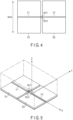
- FIG. 3 to FIG. 5 illustrate simulation conditions of case 1
- FIG. 3 is a cross-sectional view showing the simulation conditions in cross-section
- FIG. 4 is a plan view showing the simulation conditions in a plan state
- FIG. 5 is a perspective view showing the simulation conditions in perspective.
- FIG. 3 to FIG. 5 illustrate simulation conditions of case 1
- FIG. 3 is a cross-sectional view showing the simulation conditions in cross-section
- FIG. 4 is a plan view showing the simulation conditions in a plan state
- FIG. 5 is a perspective view showing the simulation conditions in perspective.
- D1 and D2 are dielectric substrates that are rectangular and of the same dimensions and thickness as each other, and are arranged at certain intervals on the same plane;
- L1 and L2 are microstrip lines formed on the upper surface of the dielectric substrates D1 and D2, respectively, in the same straight line;
- H1 and H2 are metal plates formed on the entire lower surface of the dielectric substrates D1 and D2, respectively, to serve as a grounding layer;
- W11 and W12 are a pair of wires connecting the ends of the microstrip lines L1 and L2, respectively.
- the upper side of the dielectric substrates D1 and D2 shall be a space formed by an air layer as a radiation boundary.
- the length of microstrip lines L1 and L2, which are wired to the upper surfaces of two dielectric substrates D1 and D2, respectively (length of the short side of the dielectric substrates D1 and D2), and the length consisting of the substrate interval of the dielectric substrates D1 and D2 (connection length of the wire W11 (W12)) are 8.9 mm; the height of the space from the upper surface of the dielectric substrates D1 and D2 is 3.5 mm; and the thickness of the dielectric substrates D1 and D2 is 0.1875 mm. Furthermore, as shown in FIG.
- the vertical width (length of a long side) of the two dielectric substrates D1 and D2 is 6.0 mm, and the simulation is performed under a condition that a resistance of 50 ⁇ is applied to reference surfaces R1 and R2 on the side surfaces of the dielectric substrates D1 and D2.
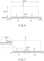
- FIG. 6 to FIG. 8 illustrate simulation conditions of case 2
- FIG. 6 is a cross-sectional view showing the simulation conditions in cross-section
- FIG. 5 is a plan view showing the simulation conditions in a plan state
- FIG. 8 is a characteristic diagram showing an example of a phase shift that occurs according to a wire length.
- case 2 The simulation conditions of case 2 are identical to those of case 1, except that the wire length (electrical length) is different.
- FIG. 6 shows a case of a simulation with wires W11a and W12a (not shown) having an electrical length 0.2 mm longer than the wires W11 and W12 of case 1
- FIG. 7 shows a case of a simulation with wires W11b and W12b (not shown) having an electrical length 1.0 mm longer than the wires W11 and W12 of case 1.
- the wires W11a and W12a and W11b and W12b extend in length in the form of a vertical extension from the connection end with the microstrip lines L1 and L2.
- case 2 describes a case where the electrical length of the wires is lengthened from case 1. If the electrical length of the wire can be lengthened, a physical length of the wire can be shortened.
- FIG. 8 is a characteristic diagram showing an example of a shift in phase characteristics caused in accordance with the length of the wire.
- a horizontal axis is the length of the wire ([mm]) and a vertical axis shows the phase (Phase [deg.]).
- Point P1 is a case for the condition of FIG. 3 (case 1) because the wire length is 0
- Point P2 is a case for the condition of FIG. 6 (case 2) because the wire length is 0.2 mm
- point P3 is a case for the condition of FIG. 7 (case 2) because the wire length is 1.0 mm.
- FIG. 8 shows that the phase is delayed as the wire length is lengthened. For example, at point P3 where the wire length is extended by 1.0 mm from the state shown in FIG. 3 , the phase is shown to be delayed by approximately 4 deg.
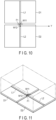
- FIG. 9 to FIG. 11 illustrate conditions for the simulation of case 3.
- the simulation of case 3 is identical to that of case 1, except that the ferrite F1 is arranged directly below the arches of the wires W11 and W12.
- the ferrite F1 is a rectangular body of 0.05 ⁇ 1.0 ⁇ 0.4 (mm) in the present simulation.
- the material constant (relative magnetic permeability) of the ferrite F1 is 640 of Ni-Zn system.
- FIG. 12 to FIG. 14 show results of S11 and S21 characteristics of an S parameter, comparing the simulation results for the case of case 1, the case of case 2 (wire length 1.0 mm), and the case of case 3.
- FIG. 12 shows an example of the simulation results of an S11 characteristic
- FIG. 13 shows an example of the simulation results of an S21 characteristic
- FIG. 14 shows an example of the simulation results of the phase characteristics.
- the S11 characteristic is, for example, a characteristic showing the amount of power input to port 1 (microstrip line L1) returning to port 1
- the S21 characteristic is, for example, a characteristic showing the amount of power input to port 1 that is reflected to port 2 (microstrip line L2).
- the S11 characteristic shown in FIG. 12 and the S21 characteristic shown in FIG. 13 are generally equal.
- the phase characteristics shown in FIG. 14 also show that the phase is delayed in case 3 compared to case 1. From this simulation result, it can be seen that the arrangement of the ferrite F1 does not change the S11 characteristic and the S21 characteristic, and the same phase delay can be obtained as in the case of lengthening the electric length.
- the semiconductor device 1 can shorten the length of each wire of the first connector W1 and the second connector W2 without affecting the phase characteristics.
- the semiconductor device 1 can shorten the length of each wire of the first connector W1 and the second connector W2 as already described, the size of the first circuit board 12, the second board circuit 13, and the FET board 14 can be increased inside the semiconductor device 1. Therefore, it is possible to increase the number of functions to be mounted on the first circuit board 12, the second circuit board 13, and the FET board 14.
- FIG. 15 shows an example of a configuration of a semiconductor device 100 of a second embodiment
- FIG. 16 is a cross-sectional view showing a cross-section along line B-B in FIG. 15 .
- the configuration of an FET board 14 is more detailed. Note that the same configurations as those of the semiconductor device 1 described above are denoted by the same symbols, and detailed description thereof is omitted. In addition, illustration of the microstrip lines is omitted.
- an electrode 12a is provided on a first circuit board 12, and an electrode 13a is provided on a second circuit board 13.
- the FET board 14 has a plurality of electrodes 14a provided on the first circuit board 12 side and an electrode 14b provided on the second circuit board 13 side.
- the plurality of electrodes 14a are lined up in one example in the longitudinal direction of the FET board 14 at equal intervals.
- the electrode 14b has a rectangular shape and is arranged parallel to the longitudinal direction of the FET board 14.
- the electrode 12a of the first circuit board 12 is configured to spread from a lead electrode part 15 side in a fan shape so as to correspond to the width of the plurality of electrodes 14a of the FET board 14.
- a plurality of fifth wires configuring a fifth connector W5 connect each of the plurality of electrodes 14a to the electrode 12a.
- the electrode 13a of the second circuit board 13 is configured to spread from a lead electrode part 16 side in a fan shape so as to correspond to the width of the electrode 14b of the FET board 14.
- a plurality of sixth wires configuring a sixth connector W6 connect the electrode 14b to the electrode 13a.
- a ferrite F1 is arranged between the first circuit board 12 and the FET board 14, on the base 10 and directly below the arched fifth wires of the fifth connector W5.
- the ferrite F1 is rectangular in shape, and both ends of the ferrite F1 in the longitudinal direction are configured to exceed the width of the plurality of fifth wires of the fifth connector W5 in the alignment direction.
- a ferrite F2 is arranged between the second circuit board 13 and the FET board 14, on the base 10 and directly below the arched sixth wires of the sixth connector W6.
- the ferrite F2 is rectangular in shape, and both ends of the ferrite F2 in the longitudinal direction are configured to exceed the width of the sixth connector W6 in the alignment direction.
- the same effects as those of the first embodiment can be achieved. More specifically, in the semiconductor device 100, by arranging the ferrite F1 on the base 10 and directly below the arched fifth wires of the fifth connector W5, the phase of the current from the first circuit board 12 to the FET board 14 can be adjusted, and the same effect as lengthening the electrical length can be obtained. In addition, by arranging the ferrite F2 on the base 10 and directly below the arched sixth wire of the sixth connector W6, the phase of the current from the FET board 14 to the second circuit board 14 can be adjusted, and the same effect as lengthening the electrical length can be obtained. Thus, since the same effect as lengthening the electrical length can be obtained, the semiconductor device 100 can shorten the length of each wire of the fifth connector W5 and the sixth connector W6 without affecting the phase characteristics.
- the semiconductor device 100 can shorten the length of each wire of the fifth connector W5 and the sixth connector W6 as already described, the size of the first circuit board 12, the second board circuit 13, and the FET board 14 can be increased inside the semiconductor device 100. Therefore, in the same manner as in the first embodiment, it becomes possible to increase the number of functions to be mounted on the first circuit board 12, the second circuit board 13, and the FET board 14.
- the ferrite F1 (or the ferrite F2) was arranged directly below the arched wires of the first connector W1 and the fifth connector W5 (or the second connector W2, the sixth connector W6) connecting the first circuit board 12 (or the second circuit board 13) and the FET board 14; however, the same effect can be achieved even in a case where the first circuit board 12 (or the second circuit board 13) is not connected to the FET board 14, if the ferrite is arranged directly below the wires connecting the circuit board to the circuit board.
- the above techniques can be applied as long as there are at least two circuit boards inside the semiconductor device 100, and it is a semiconductor device in which the two circuit boards are connected by wires.
- the shape of the cross-sections of the ferrites F1 and F2 is rectangular is described; however, it is not limited thereto.
- the shape of the cross-sections of the two ferrites may be circular, and the ferrites F1 and F2 with such a shape of cross-sections may be arranged on the base 10 and directly below the arched wires of the first connector W1 and the fifth connector W5 (or the second connector W2, the sixth connector W6) inside the semiconductor packages 1 and 100.
- the techniques of the above embodiments can be used not only in the case of increasing the size of the first circuit board 12, the second circuit board 13, and the FET board 14 inside the semiconductor devices 1 and 100, but also in the case of increasing the number of stages of circuit boards inside the semiconductor devices 1 and 100 since the distance between the circuit boards can be made smaller.
- the degree of freedom in designing the interior of the semiconductor devices 1 and 100 can be improved.
- the semiconductor devices 1 and 100 can achieve, for example, widening the S-band.
- the semiconductor devices 1 and 100 of each of the above embodiments are described as having a first circuit board 12, a second circuit board 13, and a FET board 14, having first connector W1 wires and second connector W2 wires, or fifth connector W5 wires and sixth connector W6 wires to connect them, and having ferrites F1 and F2; however, it is not limited thereto.
- the ferrites may be arranged on the base and directly below the arched wires that connect each circuit board, respectively.
Landscapes
- Shielding Devices Or Components To Electric Or Magnetic Fields (AREA)
- Coils Or Transformers For Communication (AREA)
Abstract
Description
- Embodiments described herein relate generally to a semiconductor device and a method for adjusting phase characteristics thereof.
- In a semiconductor device configuring a variable tuning filter, a coupled-line conductor is formed on a surface of a semiconductor substrate. The semiconductor substrate has a storage hole for storing a ferrite sphere at a position away from a center portion. A ferrite single-crystal sphere in a magnetostatic mode is stored in the storage hole.
-
- Patent Literature 1:
JP 2001-144506 A - Patent Literature 2:
JP 2010-166287 A - Patent Literature 3:
JP 2014-222836 A - Patent Literature 4:
JP H06-314945 A - By the way, a semiconductor device has a plurality of circuit boards therein, and each circuit board is connected by wires. In recent years, it has become desirable to mount many devices on circuit boards to realize various functions. For this reason, it has become necessary to increase the size of the internal circuit boards in semiconductor devices. On the other hand, when the size of the circuit board is increased, the distance between the circuit boards becomes narrower due to the limitation of the internal size of the semiconductor device, and, as a result, the length of the wires connecting the circuit boards also becomes shorter. If the wires become shorter, phase characteristics cannot be maintained, and the performance of the semiconductor device may deteriorate.
- The purpose of the embodiments is to provide, in a case where a plurality of circuit boards are arranged therein, a semiconductor device and a method for adjusting the phase characteristics thereof that can maintain the phase characteristics and prevent deterioration of the performance even if the wires connecting the circuit boards are shortened.
- According to one embodiment, a semiconductor device comprises a base, a first circuit board provided on the base, a second circuit board provided on the base at a certain interval from the first circuit board, a first connector provided with a first wire that is bridged between an upper surface of the first circuit board and an upper surface of the second circuit board to connect the two boards, and a first ferrite arranged on the base and directly below the first wire between the first circuit board and the second circuit board.
- Also, according to one embodiment, a method for adjusting phase characteristics of a semiconductor device provides a first circuit board and a second circuit board at certain intervals on a base, bridges a first wire between an upper surface of the first circuit board and an upper surface of the second circuit board to connect the two boards, and arranges a first ferrite on the base and directly below the first wire between the first circuit board and the second circuit board to adjust phase characteristics of the first wire.
-
-
FIG. 1 is a plan view showing a configuration of a semiconductor device according to a first embodiment. -
FIG. 2 is a cross-sectional view showing a cross-section of the semiconductor device shown inFIG. 1 along line A-A. -
FIG. 3 is a cross-sectional view showing simulation conditions ofcase 1 in cross-section in a virtual model of the semiconductor device according to the same embodiment. -
FIG. 4 is a plan view showing the simulation conditions ofcase 1 in a plan state in the virtual model of the semiconductor device according to the same embodiment. -
FIG. 5 is a perspective view showing the simulation conditions ofcase 1 in perspective in the virtual model of the semiconductor device according to the same embodiment. -
FIG. 6 is a cross-sectional view showing simulation conditions ofcase 2 in the virtual model of the semiconductor device according to the same embodiment. -
FIG. 7 is a cross-sectional view showing the simulation conditions ofcase 2 in the virtual model of the semiconductor device according to the same embodiment. -
FIG. 8 is a characteristic diagram showing an example of a phase shift that occurs in accordance with a wire length in the virtual model of the semiconductor device according to the same embodiment. -
FIG. 9 is a cross-sectional view showing simulation conditions ofcase 3 in the virtual model of the semiconductor device according to the same embodiment. -
FIG. 10 is a plan view showing the simulation conditions ofcase 3 in the virtual model of the semiconductor device according to the same embodiment. -
FIG. 11 is a perspective view showing the simulation conditions ofcase 3 in the virtual model of the semiconductor device according to the same embodiment. -
FIG. 12 is a characteristic diagram showing an example of simulation results of an S11 characteristic in the virtual model of the semiconductor device according to the same embodiment. -
FIG. 13 is a characteristic diagram showing an example of simulation results of an S21 characteristic in the virtual model of the semiconductor device according to the same embodiment. -
FIG. 14 is a characteristic diagram showing an example of simulation results of phase characteristics in the virtual model of the semiconductor device according to the same embodiment. -
FIG. 15 is a plan view showing a configuration of a semiconductor device in the semiconductor device according to a second embodiment. -
FIG. 16 is a cross-sectional view showing a cross-section of the semiconductor device shown inFIG. 15 along line B-B. - The following is a description of the embodiments with reference to the drawings. The disclosure is only an example, and the invention is not limited by the contents described in the following embodiments. Modifications readily conceivable by those skilled in the art are naturally included within the scope of the disclosure. For the sake of clarity of explanation, in some cases, the size, shape, etc., of each part in the drawings may be schematically represented by being changed with respect to the actual implementation. In some cases, the same reference numeral may be used for corresponding elements in multiple drawings, and detailed explanations may be omitted.
-
FIG. 1 is a plan view showing a schematic configuration of a semiconductor device according to a first embodiment, andFIG. 2 is a cross-sectional view showing a cross-section of the semiconductor device shown inFIG. 1 along line A-A. - As shown in
FIG. 1 , asemiconductor device 1 comprises abase 10, one side of which is a mounting surface for electronic components and the other side of which is a heat dissipation surface. The upper surface of thebase 10, i.e., the mounting surface for electronic components, is provided with acover 11 formed into a box shape, for example, by a shielding material, so as to cover the entire surface. - On the
base 10, afirst circuit board 12 and asecond circuit board 13 of the same shape as thefirst circuit board 12 are placed at predetermined intervals. Thefirst circuit board 12 and thesecond circuit board 13 are, for example, matching circuits that contain alumina (aluminum oxide: Al2O3) as a material and have a predetermined dielectric constant. Between thefirst circuit board 12 and thesecond circuit board 13 is disposed anFET board 14 on which a field effect transistor (FFT) power amplification circuit is formed. The FETboard 14 has a rectangular shape and is arranged in parallel between thefirst circuit board 12 and thesecond circuit board 13. On both sides of thebase 10 in the vertical direction in the drawing, a lead electrode part (first electrode part) 15 and a lead electrode part (second electrode part) 16 are provided so as to penetrate a part of a wall surface (top side and bottom side inFIG. 1 ) of thecover 11 that is in contact with thebase 10. - One or more first wires configuring a first connector W1 are bridged between the upper surface of the
first circuit board 12 and the upper surface of theFET board 14, and the boards are electrically connected by the first wires. One or more second wires configuring a second connector W2 are also bridged between the upper surface of theFET board 14 and the upper surface of thesecond circuit board 13, and the boards are electrically connected by the second wires. Both wires used for the first connector W1 and the second connector W2 are formed into an arch shape that, in the connected state, draws a semicircle on the upper side with respect to thebase 10. Note that, inFIG. 1 , a case in which the connectors W1 and W2 are each configured by four wires (two pairs of two wires) is shown; however, the number of wires in the connectors W1 and W2 is not limited to this and can be determined arbitrarily, as long as there is at least one wire. - One or more third wires configuring a third connector W3 are bridged between the upper surface of the
first circuit board 12 and the upper surface of the lead electrode part (first electrode part) 15, and the boards are electrically connected by the third wires. One or more fourth wires configuring a fourth connector W4 are bridged between the upper surface of thesecond circuit board 13 and the upper surface of the lead electrode part (second electrode part) 16, and the boards are electrically connected by the fourth wires. - The surfaces of the
first circuit board 12, thesecond circuit board 13, and theFET board 14 are provided with electronic circuits by means of microstrip lines (not shown). In thesemiconductor device 1 in which the microstrip lines are formed in this manner, a current input from thelead electrode part 15 is configured to pass through the third wire of the third connector W3, the microstrip line of thefirst circuit board 12, the first wire of the first connector W1, the microstrip line of theFET board 14, the second wire of the second connector W2, the microstrip line of thesecond circuit board 13, the fourth wire of the fourth connector W4, and thelead electrode part 16. - In the present embodiment, between the
first circuit board 12 and theFET board 14, a ferrite (first ferrite) F1 is arranged on thebase 10 and directly below the arched first wire of the first connector W1, and, between thesecond circuit board 13 and theFET board 14, a ferrite (second ferrite) F2 is arranged on thebase 10 and directly below the arched second wire of the second connector W2. The ferrites F1 and F2 are rod-shaped members (rectangular shape) with a rectangular cross-section. In the present embodiment, a case in which the length of the ferrites F1 and F2 is approximately the same as the length of thefirst circuit board 12, thesecond circuit board 13, and theFET board 14 in the longitudinal direction is explained. - One surface of the ferrites F1 and F2 (a surface with a shorter cross-sectional length, as shown in
FIG. 2 ) is bonded respectively on thebase 10 using solder, for example, to fix the ferrites F1 and F2 to thebase 10. Here, the ferrites F1 and F2 are magnetic materials (electronic materials) made by mixing and sintering cobalt, nickel, manganese, etc., with iron oxide as the main component, and are manufactured by baking and hardening powdered materials at a high temperature of 1,000 to 1,400°C. There are many types depending on the composition and blending of materials, but rectangular shaped ferrites F1 and F2 can be produced relatively easily because they are made by pressing and solidifying powders. - As already mentioned, the
semiconductor device 1 in the present embodiment has the ferrites F1 and F2 arranged therein. Therefore, in a case where a current is applied to thesemiconductor device 1, it is assumed that current characteristics are affected by a magnetic force generated by the ferrites F1 and F2. The following explains simulation results of three cases, such as a case in which ferrites are not arranged in a virtual model of the semiconductor device 1 (hereinafter referred to as case 1), the length of a wire is adjusted without arranging the ferrites in the virtual model of the semiconductor device 1 (hereinafter referred to as case 2), and a case in which ferrites are arranged in the virtual model of the semiconductor device 1 (hereafter referred to as case 3). The simulations conducted here examine the effect of ferrite arrangement in a case where two circuit boards are connected by a wire (one transmission line). - First, with reference to
FIG. 3 to FIG. 5 , the virtual model of thesemiconductor device 1 is explained forcase 1.FIG. 3 to FIG. 5 illustrate simulation conditions ofcase 1,FIG. 3 is a cross-sectional view showing the simulation conditions in cross-section,FIG. 4 is a plan view showing the simulation conditions in a plan state, andFIG. 5 is a perspective view showing the simulation conditions in perspective. Here, inFIG. 3 to FIG. 5 , D1 and D2 are dielectric substrates that are rectangular and of the same dimensions and thickness as each other, and are arranged at certain intervals on the same plane; L1 and L2 are microstrip lines formed on the upper surface of the dielectric substrates D1 and D2, respectively, in the same straight line; H1 and H2 are metal plates formed on the entire lower surface of the dielectric substrates D1 and D2, respectively, to serve as a grounding layer; and W11 and W12 are a pair of wires connecting the ends of the microstrip lines L1 and L2, respectively. The upper side of the dielectric substrates D1 and D2 shall be a space formed by an air layer as a radiation boundary. - As shown in
FIG. 3 , the length of microstrip lines L1 and L2, which are wired to the upper surfaces of two dielectric substrates D1 and D2, respectively (length of the short side of the dielectric substrates D1 and D2), and the length consisting of the substrate interval of the dielectric substrates D1 and D2 (connection length of the wire W11 (W12)) are 8.9 mm; the height of the space from the upper surface of the dielectric substrates D1 and D2 is 3.5 mm; and the thickness of the dielectric substrates D1 and D2 is 0.1875 mm. Furthermore, as shown inFIG. 4 , the vertical width (length of a long side) of the two dielectric substrates D1 and D2 is 6.0 mm, and the simulation is performed under a condition that a resistance of 50 Ω is applied to reference surfaces R1 and R2 on the side surfaces of the dielectric substrates D1 and D2. - Next, with reference to
FIG. 6 to FIG. 8 , the virtual model of thesemiconductor device 1 is explained forcase 2.FIG. 6 to FIG. 8 illustrate simulation conditions ofcase 2,FIG. 6 is a cross-sectional view showing the simulation conditions in cross-section,FIG. 5 is a plan view showing the simulation conditions in a plan state, andFIG. 8 is a characteristic diagram showing an example of a phase shift that occurs according to a wire length. - The simulation conditions of
case 2 are identical to those ofcase 1, except that the wire length (electrical length) is different.FIG. 6 shows a case of a simulation with wires W11a and W12a (not shown) having an electrical length 0.2 mm longer than the wires W11 and W12 ofcase 1, andFIG. 7 shows a case of a simulation with wires W11b and W12b (not shown) having an electrical length 1.0 mm longer than the wires W11 and W12 ofcase 1. Note that, as shown inFIG. 6 and FIG. 7 , the wires W11a and W12a and W11b and W12b extend in length in the form of a vertical extension from the connection end with the microstrip lines L1 and L2. Thus,case 2 describes a case where the electrical length of the wires is lengthened fromcase 1. If the electrical length of the wire can be lengthened, a physical length of the wire can be shortened. -
FIG. 8 is a characteristic diagram showing an example of a shift in phase characteristics caused in accordance with the length of the wire. InFIG. 8 , a horizontal axis is the length of the wire ([mm]) and a vertical axis shows the phase (Phase [deg.]). Point P1 is a case for the condition ofFIG. 3 (case 1) because the wire length is 0, Point P2 is a case for the condition ofFIG. 6 (case 2) because the wire length is 0.2 mm, and point P3 is a case for the condition ofFIG. 7 (case 2) because the wire length is 1.0 mm.FIG. 8 shows that the phase is delayed as the wire length is lengthened. For example, at point P3 where the wire length is extended by 1.0 mm from the state shown inFIG. 3 , the phase is shown to be delayed by approximately 4 deg. - Next,
case 3 is explained.FIG. 9 to FIG. 11 illustrate conditions for the simulation ofcase 3. The simulation ofcase 3 is identical to that ofcase 1, except that the ferrite F1 is arranged directly below the arches of the wires W11 and W12. The ferrite F1 is a rectangular body of 0.05 × 1.0 × 0.4 (mm) in the present simulation. Also, the material constant (relative magnetic permeability) of the ferrite F1 is 640 of Ni-Zn system. - Next, simulation results are explained.
FIG. 12 to FIG. 14 show results of S11 and S21 characteristics of an S parameter, comparing the simulation results for the case ofcase 1, the case of case 2 (wire length 1.0 mm), and the case ofcase 3.FIG. 12 shows an example of the simulation results of an S11 characteristic,FIG. 13 shows an example of the simulation results of an S21 characteristic, andFIG. 14 shows an example of the simulation results of the phase characteristics. Here, the S11 characteristic is, for example, a characteristic showing the amount of power input to port 1 (microstrip line L1) returning toport 1, and the S21 characteristic is, for example, a characteristic showing the amount of power input toport 1 that is reflected to port 2 (microstrip line L2). - It can be seen that the S11 characteristic shown in
FIG. 12 and the S21 characteristic shown inFIG. 13 are generally equal. The phase characteristics shown inFIG. 14 also show that the phase is delayed incase 3 compared tocase 1. From this simulation result, it can be seen that the arrangement of the ferrite F1 does not change the S11 characteristic and the S21 characteristic, and the same phase delay can be obtained as in the case of lengthening the electric length. - Therefore, from the above simulation results, by arranging the ferrite F1 on the
base 10 and directly below the first wire that configures the first connector W1 in thesemiconductor device 1, the phase of the current from thefirst circuit board 12 to theFET board 14 can be adjusted, and the same effect as lengthening the electrical length can be obtained. Also, by arranging the ferrite F2 on thebase 10 and directly below the second wire that configures the second connector W2, the phase of the current from theFET board 14 to thesecond circuit board 14 can be adjusted, and the same effect as lengthening the electrical length can be obtained. Since the same effect as lengthening the electrical length can be obtained, thesemiconductor device 1 can shorten the length of each wire of the first connector W1 and the second connector W2 without affecting the phase characteristics. - Also, because the
semiconductor device 1 can shorten the length of each wire of the first connector W1 and the second connector W2 as already described, the size of thefirst circuit board 12, thesecond board circuit 13, and theFET board 14 can be increased inside thesemiconductor device 1. Therefore, it is possible to increase the number of functions to be mounted on thefirst circuit board 12, thesecond circuit board 13, and theFET board 14. -
FIG. 15 shows an example of a configuration of asemiconductor device 100 of a second embodiment, andFIG. 16 is a cross-sectional view showing a cross-section along line B-B inFIG. 15 . Compared to thesemiconductor device 1 of the first embodiment, the configuration of anFET board 14 is more detailed. Note that the same configurations as those of thesemiconductor device 1 described above are denoted by the same symbols, and detailed description thereof is omitted. In addition, illustration of the microstrip lines is omitted. - As shown in
FIG. 15 andFIG. 16 , anelectrode 12a is provided on afirst circuit board 12, and anelectrode 13a is provided on asecond circuit board 13. In addition, theFET board 14 has a plurality ofelectrodes 14a provided on thefirst circuit board 12 side and anelectrode 14b provided on thesecond circuit board 13 side. The plurality ofelectrodes 14a are lined up in one example in the longitudinal direction of theFET board 14 at equal intervals. Theelectrode 14b has a rectangular shape and is arranged parallel to the longitudinal direction of theFET board 14. - The
electrode 12a of thefirst circuit board 12 is configured to spread from alead electrode part 15 side in a fan shape so as to correspond to the width of the plurality ofelectrodes 14a of theFET board 14. A plurality of fifth wires configuring a fifth connector W5 connect each of the plurality ofelectrodes 14a to theelectrode 12a. In addition, theelectrode 13a of thesecond circuit board 13 is configured to spread from alead electrode part 16 side in a fan shape so as to correspond to the width of theelectrode 14b of theFET board 14. A plurality of sixth wires configuring a sixth connector W6 connect theelectrode 14b to theelectrode 13a. - Furthermore, a ferrite F1 is arranged between the
first circuit board 12 and theFET board 14, on thebase 10 and directly below the arched fifth wires of the fifth connector W5. The ferrite F1 is rectangular in shape, and both ends of the ferrite F1 in the longitudinal direction are configured to exceed the width of the plurality of fifth wires of the fifth connector W5 in the alignment direction. Similarly, a ferrite F2 is arranged between thesecond circuit board 13 and theFET board 14, on thebase 10 and directly below the arched sixth wires of the sixth connector W6. In the same manner as the ferrite F1, the ferrite F2 is rectangular in shape, and both ends of the ferrite F2 in the longitudinal direction are configured to exceed the width of the sixth connector W6 in the alignment direction. - Also in the
semiconductor device 100 configured as described above, the same effects as those of the first embodiment can be achieved. More specifically, in thesemiconductor device 100, by arranging the ferrite F1 on thebase 10 and directly below the arched fifth wires of the fifth connector W5, the phase of the current from thefirst circuit board 12 to theFET board 14 can be adjusted, and the same effect as lengthening the electrical length can be obtained. In addition, by arranging the ferrite F2 on thebase 10 and directly below the arched sixth wire of the sixth connector W6, the phase of the current from theFET board 14 to thesecond circuit board 14 can be adjusted, and the same effect as lengthening the electrical length can be obtained. Thus, since the same effect as lengthening the electrical length can be obtained, thesemiconductor device 100 can shorten the length of each wire of the fifth connector W5 and the sixth connector W6 without affecting the phase characteristics. - Because the
semiconductor device 100 can shorten the length of each wire of the fifth connector W5 and the sixth connector W6 as already described, the size of thefirst circuit board 12, thesecond board circuit 13, and theFET board 14 can be increased inside thesemiconductor device 100. Therefore, in the same manner as in the first embodiment, it becomes possible to increase the number of functions to be mounted on thefirst circuit board 12, thesecond circuit board 13, and theFET board 14. - Furthermore, in the first and second embodiments above, the ferrite F1 (or the ferrite F2) was arranged directly below the arched wires of the first connector W1 and the fifth connector W5 (or the second connector W2, the sixth connector W6) connecting the first circuit board 12 (or the second circuit board 13) and the
FET board 14; however, the same effect can be achieved even in a case where the first circuit board 12 (or the second circuit board 13) is not connected to theFET board 14, if the ferrite is arranged directly below the wires connecting the circuit board to the circuit board. In addition, the above techniques can be applied as long as there are at least two circuit boards inside thesemiconductor device 100, and it is a semiconductor device in which the two circuit boards are connected by wires. - Furthermore, in each of the above embodiments, a case where the shape of the cross-sections of the ferrites F1 and F2 is rectangular is described; however, it is not limited thereto. For example, the shape of the cross-sections of the two ferrites may be circular, and the ferrites F1 and F2 with such a shape of cross-sections may be arranged on the
base 10 and directly below the arched wires of the first connector W1 and the fifth connector W5 (or the second connector W2, the sixth connector W6) inside thesemiconductor packages - Furthermore, the techniques of the above embodiments can be used not only in the case of increasing the size of the
first circuit board 12, thesecond circuit board 13, and theFET board 14 inside thesemiconductor devices semiconductor devices semiconductor devices semiconductor devices - Furthermore, the
semiconductor devices first circuit board 12, asecond circuit board 13, and aFET board 14, having first connector W1 wires and second connector W2 wires, or fifth connector W5 wires and sixth connector W6 wires to connect them, and having ferrites F1 and F2; however, it is not limited thereto. In a case where the semiconductor has four or more circuit boards, the ferrites may be arranged on the base and directly below the arched wires that connect each circuit board, respectively. - While certain embodiments have been described, these embodiments have been presented by way of example only, and are not intended to limit the scope of the inventions. Indeed, the novel embodiments described herein may be embodied in a variety of other forms; furthermore, various omissions, substitutions and changes in the form of the embodiments described herein may be made without departing from the spirit of the inventions. The accompanying claims and their equivalents are intended to cover such forms or modifications as would fall within the scope and spirit of the inventions.
- 1, 100...Semiconductor device, 10...Base, 11...Cover, 12...First circuit board, 13...Second circuit board, 14...FET board, 15, 16...Lead electrode part, D1, D2...Dielectric circuit, F1, F2... Ferrite, L1, L2... Microstrip line, H1, H2...Metal plate, W1, W2, W3, W4, W5, W6...Connector (Wire).
Claims (11)
- A semiconductor device comprising:a base;a first circuit board provided on the base;a second circuit board provided on the base at a certain interval from the first circuit board;a first connector provided with a first wire that is bridged between an upper surface of the first circuit board and an upper surface of the second circuit board to connect the two boards; anda first ferrite arranged on the base and directly below the first wire between the first circuit board and the second circuit board.
- The semiconductor device of claim 1, whereinthe first connector is provided with a plurality of the first wires that are bridged in parallel at a plurality of locations between the upper surface of the first circuit board and the upper surface of the second circuit board to connect the two boards, andthe first ferrite is a rectangular body with both side surfaces in a longitudinal direction facing side surfaces of the first circuit board and the second circuit board, respectively, and with both ends in the longitudinal direction having a length exceeding a width of an alignment direction of the plurality of first wires, and is arranged directly below all of the plurality of first wires.
- The semiconductor device of claim 1, whereinthe first circuit board is a matching circuit that adjusts a phase of a voltage, andthe second circuit board is a field effect transistor power amplifier circuit.
- The semiconductor device of claim 1, wherein the first wire is formed in an upwardly arched shape with respect to the base.
- The semiconductor device of claim 1, further comprising:a third circuit board provided on the base at a certain interval from the second circuit board;a second connector provided with a second wire that is bridged between an upper surface of the third circuit board and an upper surface of the second circuit board to connect the two boards; anda second ferrite arranged on the base and directly below the second wire between the third circuit board and the second circuit board.
- The semiconductor device of claim 5, whereinthe second connector is provided with a plurality of the second wires that are bridged in parallel at a plurality of locations between the third circuit board and the second circuit board to connect the two boards, andthe second ferrite is a rectangular body with both sides in a longitudinal direction facing side surfaces of the third circuit board and the second circuit board, respectively, and with both ends in the longitudinal direction having a length exceeding a width of an alignment direction of the plurality of second wires, and is arranged directly below all of the plurality of second wires.
- The semiconductor device of claim 5, wherein the second wires are formed in an upwardly arched shape with respect to the base.
- A method for adjusting phase characteristics of a semiconductor device, comprising:providing a first circuit board and a second circuit board at certain intervals on a base;bridging a first wire between an upper surface of the first circuit board and an upper surface of the second circuit board to connect the two boards; andarranging a first ferrite on the base and directly below the first wire between the first circuit board and the second circuit board to adjust phase characteristics of the first wire.
- The method for adjusting phase characteristics of the semiconductor device of claim 8, wherein the first wire is formed in an upwardly arched shape with respect to the base.
- The method for adjusting phase characteristics of the semiconductor device of claim 8, comprising:providing a third circuit board on the base at a certain interval from the second circuit board; bridging a second wire between an upper surface of the third circuit board and an upper surface of the second circuit board to connect the two boards; andarranging a ferrite on the base and directly below the second wire between the first circuit board and the second circuit board to adjust phase characteristics of the second wire.
- The method for adjusting phase characteristics of the semiconductor device of claim 10, wherein the second wire is formed in an upwardly arched shape with respect to the base.
Applications Claiming Priority (2)
| Application Number | Priority Date | Filing Date | Title |
|---|---|---|---|
| JP2021047036A JP7682658B2 (en) | 2021-03-22 | 2021-03-22 | Semiconductor Device |
| PCT/JP2022/010311 WO2022202326A1 (en) | 2021-03-22 | 2022-03-09 | Semiconductor device and phase characteristic adjustment method therefor |
Publications (2)
| Publication Number | Publication Date |
|---|---|
| EP4318565A1 true EP4318565A1 (en) | 2024-02-07 |
| EP4318565A4 EP4318565A4 (en) | 2025-03-19 |
Family
ID=83395708
Family Applications (1)
| Application Number | Title | Priority Date | Filing Date |
|---|---|---|---|
| EP22775118.7A Pending EP4318565A4 (en) | 2021-03-22 | 2022-03-09 | SEMICONDUCTOR DEVICE AND PHASE CHARACTERISTIC ADJUSTING METHOD THEREOF |
Country Status (4)
| Country | Link |
|---|---|
| US (1) | US20240014150A1 (en) |
| EP (1) | EP4318565A4 (en) |
| JP (1) | JP7682658B2 (en) |
| WO (1) | WO2022202326A1 (en) |
Family Cites Families (15)
| Publication number | Priority date | Publication date | Assignee | Title |
|---|---|---|---|---|
| JP2820264B2 (en) * | 1989-03-22 | 1998-11-05 | 株式会社タイセー | High frequency transformer and method of manufacturing the same |
| JPH06314945A (en) | 1993-04-30 | 1994-11-08 | Uniden Corp | Ultra-wideband constant phase difference power divider |
| JPH0730052A (en) * | 1993-06-23 | 1995-01-31 | Hitachi Ltd | Module board for computer |
| JP2001144506A (en) | 1999-11-12 | 2001-05-25 | Advantest Corp | Tuning frequency filter |
| DE10123232A1 (en) * | 2001-05-12 | 2002-11-21 | Infineon Technologies Ag | Semiconductor module used as a MOSFET, JFET or thyristor has a damping material having electromagnetically damping properties provided in a sealing composition arranged within a housing |
| JP4012840B2 (en) * | 2003-03-14 | 2007-11-21 | 三菱電機株式会社 | Semiconductor device |
| US8431973B2 (en) * | 2008-12-10 | 2013-04-30 | Kabushiki Kaisha Toshiba | High frequency semiconductor device |
| JP5131481B2 (en) | 2009-01-15 | 2013-01-30 | 株式会社村田製作所 | ANTENNA DEVICE AND RADIO COMMUNICATION DEVICE |
| JP5872801B2 (en) * | 2011-06-22 | 2016-03-01 | Necトーキン株式会社 | Interposer |
| JP2013074249A (en) * | 2011-09-29 | 2013-04-22 | Oki Electric Ind Co Ltd | Semiconductor package, and method for manufacturing semiconductor package |
| US20160029477A1 (en) * | 2013-02-27 | 2016-01-28 | Nec Corporation | Wiring substrate, semiconductor device, printed board, and method for producing wiring substrate |
| JP2014222836A (en) | 2013-05-14 | 2014-11-27 | 三菱電機株式会社 | Power amplifier |
| JP2017183629A (en) * | 2016-03-31 | 2017-10-05 | 東芝メモリ株式会社 | Semiconductor device and method of manufacturing the same |
| CN111033735B (en) * | 2017-09-04 | 2023-05-23 | 三菱电机株式会社 | Semiconductor module and power conversion device |
| CN112151545B (en) * | 2019-06-28 | 2024-05-14 | 西部数据技术公司 | Semiconductor device including magnetic clamping layer |
-
2021
- 2021-03-22 JP JP2021047036A patent/JP7682658B2/en active Active
-
2022
- 2022-03-09 WO PCT/JP2022/010311 patent/WO2022202326A1/en not_active Ceased
- 2022-03-09 EP EP22775118.7A patent/EP4318565A4/en active Pending
-
2023
- 2023-09-22 US US18/472,863 patent/US20240014150A1/en active Pending
Also Published As
| Publication number | Publication date |
|---|---|
| EP4318565A4 (en) | 2025-03-19 |
| JP7682658B2 (en) | 2025-05-26 |
| US20240014150A1 (en) | 2024-01-11 |
| WO2022202326A1 (en) | 2022-09-29 |
| JP2022146198A (en) | 2022-10-05 |
Similar Documents
| Publication | Publication Date | Title |
|---|---|---|
| US10790245B2 (en) | High-frequency ceramic board and high-frequency semiconductor element package | |
| US12224472B2 (en) | Digital phase shifter | |
| CN102790043B (en) | Power semiconductor | |
| EP3211669B1 (en) | Semiconductor package with isolation wall | |
| JP2007515794A (en) | Internally shielded energy regulator | |
| US10916938B2 (en) | ESD-protective surface-mount composite component | |
| CN104364897B (en) | Element storage packaging part and assembling structure | |
| JP7411882B2 (en) | connector | |
| US20100171574A1 (en) | Microstrip line | |
| JP6314591B2 (en) | Semiconductor device and manufacturing method of semiconductor device | |
| CN111697796A (en) | Drive circuit device | |
| CN105230136A (en) | Circuit board, package for housing electronic components, and electronic device | |
| US9564870B2 (en) | Structural body and wiring board | |
| KR20160007197A (en) | Tantalum capacitor | |
| US20240014150A1 (en) | Semiconductor device and method for adjusting phase characteristics thereof | |
| EP3098842B1 (en) | Package for an electronic element | |
| JPWO2007125633A1 (en) | High frequency semiconductor devices | |
| US10079415B2 (en) | Structure and wiring substrate | |
| CN105977592B (en) | Dielectric waveguide input/output structure and dielectric waveguide filter | |
| US8248190B2 (en) | Resonator and filter using the same | |
| US7265445B2 (en) | Integrated circuit package | |
| CN110914976B (en) | Circuit module | |
| JP4108099B2 (en) | Electronic component package | |
| WO2017033436A1 (en) | Millimeter wave semiconductor device | |
| JP5773416B2 (en) | Circuit board |
Legal Events
| Date | Code | Title | Description |
|---|---|---|---|
| STAA | Information on the status of an ep patent application or granted ep patent |
Free format text: STATUS: THE INTERNATIONAL PUBLICATION HAS BEEN MADE |
|
| PUAI | Public reference made under article 153(3) epc to a published international application that has entered the european phase |
Free format text: ORIGINAL CODE: 0009012 |
|
| STAA | Information on the status of an ep patent application or granted ep patent |
Free format text: STATUS: REQUEST FOR EXAMINATION WAS MADE |
|
| 17P | Request for examination filed |
Effective date: 20230922 |
|
| AK | Designated contracting states |
Kind code of ref document: A1 Designated state(s): AL AT BE BG CH CY CZ DE DK EE ES FI FR GB GR HR HU IE IS IT LI LT LU LV MC MK MT NL NO PL PT RO RS SE SI SK SM TR |
|
| DAV | Request for validation of the european patent (deleted) | ||
| DAX | Request for extension of the european patent (deleted) | ||
| REG | Reference to a national code |
Ref country code: DE Ref legal event code: R079 Free format text: PREVIOUS MAIN CLASS: H01L0023120000 Ipc: H01L0023660000 |
|
| A4 | Supplementary search report drawn up and despatched |
Effective date: 20250218 |
|
| RIC1 | Information provided on ipc code assigned before grant |
Ipc: H01F 3/08 20060101ALN20250212BHEP Ipc: H01P 1/04 20060101ALI20250212BHEP Ipc: H01L 23/00 20060101ALI20250212BHEP Ipc: H01L 23/12 20060101ALI20250212BHEP Ipc: H01L 23/66 20060101AFI20250212BHEP |
|
| RAP1 | Party data changed (applicant data changed or rights of an application transferred) |
Owner name: KABUSHIKI KAISHA TOSHIBA |