EP4317930A1 - Strain resistance film, pressure sensor, and layered body - Google Patents
Strain resistance film, pressure sensor, and layered body Download PDFInfo
- Publication number
- EP4317930A1 EP4317930A1 EP22774904.1A EP22774904A EP4317930A1 EP 4317930 A1 EP4317930 A1 EP 4317930A1 EP 22774904 A EP22774904 A EP 22774904A EP 4317930 A1 EP4317930 A1 EP 4317930A1
- Authority
- EP
- European Patent Office
- Prior art keywords
- resistance film
- distortion resistance
- film
- distortion
- pressure sensor
- Prior art date
- Legal status (The legal status is an assumption and is not a legal conclusion. Google has not performed a legal analysis and makes no representation as to the accuracy of the status listed.)
- Withdrawn
Links
Images


Classifications
-
- H—ELECTRICITY
- H01—ELECTRIC ELEMENTS
- H01C—RESISTORS
- H01C10/00—Adjustable resistors
- H01C10/10—Adjustable resistors adjustable by mechanical pressure or force
-
- G—PHYSICS
- G01—MEASURING; TESTING
- G01L—MEASURING FORCE, STRESS, TORQUE, WORK, MECHANICAL POWER, MECHANICAL EFFICIENCY, OR FLUID PRESSURE
- G01L19/00—Details of, or accessories for, apparatus for measuring steady or quasi-steady pressure of a fluent medium insofar as such details or accessories are not special to particular types of pressure gauges
- G01L19/04—Means for compensating for effects of changes of temperature, i.e. other than electric compensation
-
- C—CHEMISTRY; METALLURGY
- C22—METALLURGY; FERROUS OR NON-FERROUS ALLOYS; TREATMENT OF ALLOYS OR NON-FERROUS METALS
- C22C—ALLOYS
- C22C27/00—Alloys based on rhenium or a refractory metal not mentioned in groups C22C14/00 or C22C16/00
- C22C27/06—Alloys based on chromium
-
- C—CHEMISTRY; METALLURGY
- C23—COATING METALLIC MATERIAL; COATING MATERIAL WITH METALLIC MATERIAL; CHEMICAL SURFACE TREATMENT; DIFFUSION TREATMENT OF METALLIC MATERIAL; COATING BY VACUUM EVAPORATION, BY SPUTTERING, BY ION IMPLANTATION OR BY CHEMICAL VAPOUR DEPOSITION, IN GENERAL; INHIBITING CORROSION OF METALLIC MATERIAL OR INCRUSTATION IN GENERAL
- C23C—COATING METALLIC MATERIAL; COATING MATERIAL WITH METALLIC MATERIAL; SURFACE TREATMENT OF METALLIC MATERIAL BY DIFFUSION INTO THE SURFACE, BY CHEMICAL CONVERSION OR SUBSTITUTION; COATING BY VACUUM EVAPORATION, BY SPUTTERING, BY ION IMPLANTATION OR BY CHEMICAL VAPOUR DEPOSITION, IN GENERAL
- C23C14/00—Coating by vacuum evaporation, by sputtering or by ion implantation of the coating forming material
- C23C14/06—Coating by vacuum evaporation, by sputtering or by ion implantation of the coating forming material characterised by the coating material
- C23C14/0641—Nitrides
-
- C—CHEMISTRY; METALLURGY
- C23—COATING METALLIC MATERIAL; COATING MATERIAL WITH METALLIC MATERIAL; CHEMICAL SURFACE TREATMENT; DIFFUSION TREATMENT OF METALLIC MATERIAL; COATING BY VACUUM EVAPORATION, BY SPUTTERING, BY ION IMPLANTATION OR BY CHEMICAL VAPOUR DEPOSITION, IN GENERAL; INHIBITING CORROSION OF METALLIC MATERIAL OR INCRUSTATION IN GENERAL
- C23C—COATING METALLIC MATERIAL; COATING MATERIAL WITH METALLIC MATERIAL; SURFACE TREATMENT OF METALLIC MATERIAL BY DIFFUSION INTO THE SURFACE, BY CHEMICAL CONVERSION OR SUBSTITUTION; COATING BY VACUUM EVAPORATION, BY SPUTTERING, BY ION IMPLANTATION OR BY CHEMICAL VAPOUR DEPOSITION, IN GENERAL
- C23C14/00—Coating by vacuum evaporation, by sputtering or by ion implantation of the coating forming material
- C23C14/22—Coating by vacuum evaporation, by sputtering or by ion implantation of the coating forming material characterised by the process of coating
- C23C14/34—Sputtering
-
- G—PHYSICS
- G01—MEASURING; TESTING
- G01L—MEASURING FORCE, STRESS, TORQUE, WORK, MECHANICAL POWER, MECHANICAL EFFICIENCY, OR FLUID PRESSURE
- G01L19/00—Details of, or accessories for, apparatus for measuring steady or quasi-steady pressure of a fluent medium insofar as such details or accessories are not special to particular types of pressure gauges
- G01L19/06—Means for preventing overload or deleterious influence of the measured medium on the measuring device or vice versa
- G01L19/0681—Protection against excessive heat
-
- G—PHYSICS
- G01—MEASURING; TESTING
- G01L—MEASURING FORCE, STRESS, TORQUE, WORK, MECHANICAL POWER, MECHANICAL EFFICIENCY, OR FLUID PRESSURE
- G01L9/00—Measuring steady of quasi-steady pressure of fluid or fluent solid material by electric or magnetic pressure-sensitive elements; Transmitting or indicating the displacement of mechanical pressure-sensitive elements, used to measure the steady or quasi-steady pressure of a fluid or fluent solid material, by electric or magnetic means
- G01L9/02—Measuring steady of quasi-steady pressure of fluid or fluent solid material by electric or magnetic pressure-sensitive elements; Transmitting or indicating the displacement of mechanical pressure-sensitive elements, used to measure the steady or quasi-steady pressure of a fluid or fluent solid material, by electric or magnetic means by making use of variations in ohmic resistance, e.g. of potentiometers, electric circuits therefor, e.g. bridges, amplifiers or signal conditioning
- G01L9/04—Measuring steady of quasi-steady pressure of fluid or fluent solid material by electric or magnetic pressure-sensitive elements; Transmitting or indicating the displacement of mechanical pressure-sensitive elements, used to measure the steady or quasi-steady pressure of a fluid or fluent solid material, by electric or magnetic means by making use of variations in ohmic resistance, e.g. of potentiometers, electric circuits therefor, e.g. bridges, amplifiers or signal conditioning of resistance-strain gauges
-
- H—ELECTRICITY
- H01—ELECTRIC ELEMENTS
- H01C—RESISTORS
- H01C17/00—Apparatus or processes specially adapted for manufacturing resistors
- H01C17/06—Apparatus or processes specially adapted for manufacturing resistors adapted for coating resistive material on a base
- H01C17/065—Apparatus or processes specially adapted for manufacturing resistors adapted for coating resistive material on a base by thick film techniques, e.g. serigraphy
- H01C17/06506—Precursor compositions therefor, e.g. pastes, inks, glass frits or green body
- H01C17/06513—Precursor compositions therefor, e.g. pastes, inks, glass frits or green body characterised by the resistive component
- H01C17/06526—Precursor compositions therefor, e.g. pastes, inks, glass frits or green body characterised by the resistive component composed of metals
-
- H—ELECTRICITY
- H01—ELECTRIC ELEMENTS
- H01C—RESISTORS
- H01C17/00—Apparatus or processes specially adapted for manufacturing resistors
- H01C17/06—Apparatus or processes specially adapted for manufacturing resistors adapted for coating resistive material on a base
- H01C17/065—Apparatus or processes specially adapted for manufacturing resistors adapted for coating resistive material on a base by thick film techniques, e.g. serigraphy
- H01C17/06506—Precursor compositions therefor, e.g. pastes, inks, glass frits or green body
- H01C17/06513—Precursor compositions therefor, e.g. pastes, inks, glass frits or green body characterised by the resistive component
- H01C17/0656—Precursor compositions therefor, e.g. pastes, inks, glass frits or green body characterised by the resistive component composed of silicides
Definitions
- the present invention relates to a distortion resistance film whose resistance value changes according to distortion, and a pressure sensor using the same.
- Patent Literature 1 reports that when a composition range of Al is 4 at% or more and 25 at% or less, such a distortion resistance film can obtain a preferable property not only for the gauge factor but also for a temperature coefficient of sensitivity (TCS).
- TCS temperature coefficient of sensitivity
- the inventors of the present invention have found a distortion resistance film capable of preventing film peeling in a distortion resistance film containing Cr, Al, and N, and have completed the present invention.
- the present invention has been made in view of such actual circumstances, and an object of the present invention is to provide a distortion resistance film or the like that contains Cr, Al, and N and can prevent film peeling.
- a distortion resistance film according to the present invention includes an alloy material containing Cr, Al, N, and Si.
- a distortion resistance including an alloy material containing Cr, Al, N, and Si has a gauge factor capable of detecting resistance change due to distortion, and can prevent a problem of film peeling.
- the distortion resistance film according to the present invention wherein the ally material is represented by a formula Cr 100-x-y-z Al x N y Si z , wherein composition regions of x, y, and z satisfy 5 ⁇ x ⁇ 50, 1 ⁇ y ⁇ 20, and 0 ⁇ z, respectively.
- the distortion resistance film having such a composition range exhibits excellent distortion detection capability due to resistance change from a low temperature of -50°C in a high temperature region of 400°C.
- the distortion resistance film according to the present invention wherein the ally material may be represented by a formula Cr 100-x-y-z Al x N y Si z , wherein composition regions of x, y, and z may satisfy 5 ⁇ x ⁇ 50, 1 ⁇ y ⁇ 20, and 0.3 ⁇ z ⁇ 10, respectively.
- Such a distortion resistance film exhibits good distortion detection capability due to resistance change from a low temperature of -50°C in a high temperature region of 400°C, and can effectively prevent the problem of film peeling.
- O may be contained in an amount of 10 at% or less with respect to a total amount of Cr, Al, N, and O.
- the performance of the distortion resistance film can be improved, for example, in a temperature range of -50°C or more and 400°C or less.
- an absolute value of a temperature coefficient of sensitivity may be 2000 ppm/°C or less in a temperature range of -50°C or more and 400°C or less.
- Such a distortion resistance film has a sensitivity change per unit temperature change within a predetermined range, and thus can reduce a temperature correction error when used as, for example, a pressure sensor.
- an absolute value of a temperature coefficient of resistance may be 2000 ppm/°C or less in a temperature range of -50°C or more and 400°C or less.
- Such a distortion resistance film has a resistance value change per unit temperature change within a predetermined range, and thus can reduce a temperature correction error when used as, for example, a pressure sensor.
- a pressure sensor according to the present invention includes any one of the distortion resistance films described above, and an electrode portion electrically connected to the distortion resistance film.
- the pressure sensor according to the present invention has good durability because it is possible to perform good pressure detection by the distortion resistance film and to prevent the problem of film peeling.
- a layered body according to the present invention includes any one of the distortion resistance films described above, and a base insulating layer that is in contact with the distortion resistance film and contains Si.
- the layered body according to the present invention can suitably prevent the problem of film peeling between the distortion resistance film and the base insulating layer.
- Fig. 1 is a schematic cross-sectional view of a pressure sensor 10 using a distortion resistance film 32 and a layered body 31 including the same according to an embodiment of the present invention.
- the pressure sensor 10 includes a membrane 22 that deforms according to pressure.
- the membrane 22 is constituted by an end wall formed at one end of a hollow cylindrical stem 20, but may be constituted by a tabular Si substrate 122 (see Fig. 3 ) as in the embodiment.
- the other end of the stem 20 is an open end of a hollow portion, and the hollow portion of the stem 20 communicates with a flow path 12b of a connection member 12.
- a fluid introduced into the flow path 12b is guided from the hollow portion of the stem 20 to an inner surface 22a of the membrane 22, and a fluid pressure acts on the membrane 22.
- the stem 20 is made of metal such as stainless steel.
- the shape corresponding to the stem 20 may be configured by processing a silicon substrate by etching, or by bonding a tabular silicon substrate to another material.
- a flange portion 21 is formed around the open end of the stem 20 so as to protrude outward from an axis of the stem 20.
- the flange portion 21 is sandwiched between the connection member 12 and a pressing member 14 so that the flow path 12b leading to the inner surface 22a of the membrane 22 is sealed.
- connection member 12 includes a screw groove 12a for fixing the pressure sensor 10.
- the pressure sensor 10 is fixed via the screw groove 12a to a pressure chamber or the like in which a fluid to be measured is sealed.
- the flow path 12b formed inside the connection member 12 and the inner surface 22a of the membrane 22 in the stem 20 communicate airtightly with the pressure chamber in which the fluid to be measured exists.
- a circuit substrate 16 is attached to an upper surface of the pressing member 14.
- the circuit substrate 16 has a ring shape surrounding a periphery of the stem 20, but the shape of the circuit substrate 16 is not limited thereto.
- the circuit substrate 16 incorporates, for example, a circuit or the like to which a detection signal from the distortion resistance film 32 is transmitted.
- the distortion resistance film 32 and the like are provided on an outer surface 22b of the membrane 22.
- the distortion resistance film 32 and the circuit substrate 16 are electrically connected to each other through an intermediate wiring 72 formed by wire bonding or the like.
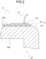
- Fig. 2 is a schematic cross-sectional view illustrating a part of the distortion resistance film 32 included in the pressure sensor 10 illustrated in Fig. 1 and its peripheral portion in an enlarged manner.
- the distortion resistance film 32 is provided on the outer surface 22b of the membrane 22 via a base insulating layer 52.
- the distortion resistance film 32 and the base insulating layer 52 in contact with the distortion resistance film constitute the layered body 31.
- the base insulating layer 52 is formed so as to cover substantially the entire outer surface 22b of the membrane 22, is made of, for example, silicon oxide such as SiO 2 , silicon nitride, silicon oxynitride, or the like, and contains Si.
- a thickness of the base insulating layer 52 is preferably 10 ⁇ m or less, and more preferably 1 to 5 ⁇ m.
- the base insulating layer 52 can be formed on the outer surface 22b of the membrane 22 by a vapor deposition method such as CVD.
- the distortion resistance film 32 may be formed directly on the outer surface 22b of the membrane 22 without forming the base insulating layer 52.
- the distortion resistance film 32 may be directly provided on the membrane 22.
- an electrode portion 36 is provided on the distortion resistance film 32.
- resistors constituting a wheatstone bridge circuit are formed in a predetermined pattern. Since a resistance value of the resistor formed in the distortion resistance film 32 changes according to deformation of the membrane 22, the distortion generated in the membrane 22 and the fluid pressure acting on the membrane 22 are detected from an output of the wheatstone bridge circuit.
- the distortion resistance film 32 including the resistor can be produced by microfabricating (patterning) a thin film formed to have a predetermined thickness.
- the distortion resistance film 32 is made of an alloy material containing Cr, Al, N, and Si.
- the distortion resistance film 32 is represented by a general formula Cr 100-x-y-z Al x N y Si z , and composition regions of x, y, and z are preferably 5 ⁇ x ⁇ 50, 1 ⁇ y ⁇ 20, and 0 ⁇ z, respectively.
- the distortion resistance film 32 exhibits a good distortion detection capability due to resistance change in a wide temperature region from a low temperature of -50°C to a high temperature region of 400°C by satisfying 5 ⁇ x ⁇ 50 for x indicating an Al amount, 1 ⁇ y ⁇ 20 for y indicating a N amount, and 0 ⁇ z for z indicating a Si amount in the general formula.
- the composition regions of x, y, and z satisfy 5 ⁇ x ⁇ 50, 1 ⁇ y ⁇ 20, and 0.3 ⁇ z ⁇ 10, respectively.
- the distortion resistance film 32 has such a composition, film peeling of the distortion resistance film 32 from the base insulating film 32 and the substrate can be suitably prevented. Furthermore, it is possible to achieve both the effect of preventing film peeling by containing Si and good TCR property at a high level.
- the distortion resistance film 32 may have an absolute value of a temperature coefficient of resistance (TCR) of2000 ppm/°C or less in a temperature range of -50°C or more and 400°C or less. Since such a distortion resistance film 32 has a small proportion of a resistance value change accompanying a temperature change in a wide range from a low temperature region to a high temperature region, the distortion resistance film is suitably used as the distortion resistance film 32 of the pressure sensor 10 used in a wide temperature range, and can reduce a temperature correction error and perform highly accurate detection.
- TCR temperature coefficient of resistance
- the distortion resistance film 32 may have an absolute value of a temperature coefficient of sensitivity (TCS) of2000 ppm/°C or less in a temperature range of -50°C or more and 400°C or less. Since such a distortion resistance film 32 has a small proportion of a sensitivity change accompanying a temperature change in a wide range from a low temperature region to a high temperature region, the distortion resistance film is suitably used as the distortion resistance film 32 of the pressure sensor 10 used in a wide temperature range, and can reduce a temperature correction error and perform highly accurate detection.
- TCS temperature coefficient of sensitivity
- the distortion resistance film 32 may contain O as an inevitable impurity in an amount of 10 at% or less with respect to a total amount of Cr, Al, N, and O.
- O as an inevitable impurity is 10 at% or less
- the distortion resistance film 32 can increase the gauge factor in a temperature range of, for example, -50°C or more and 400°C or less.
- the distortion resistance film 32 can be formed by a thin film method such as sputtering or vapor deposition by a DC sputtering device or an RC sputtering device.
- a thickness of the distortion resistance film 32 is not particularly limited, but can be, for example, 1 nm to 1000 nm, and is preferably about 50 nm to 500 nm.
- O and N contained in the distortion resistance film 32 may be those remaining without being removed from a reaction chamber when the distortion resistance film 32 is formed, and may be taken into the distortion resistance film 32. Furthermore, O and N contained in the distortion resistance film 32 may be introduced into the distortion resistance film 32 while intentionally controlling an introduction amount by being used as an atmospheric gas during film formation or annealing.
- the distortion resistance film 32 may contain a metal other than Cr, Al, and Si or a nonmetallic element in a small amount.
- metals other than Cr, Al, and Si, and non-metal elements contained in the distortion resistance film 32 include Ti, Nb, Ta, Ni, Zr, Hf, Ge, C, P, Se, Te, Zn, Cu, Bi, Fe, Mo, W, As, Sn, Sb, Pb, B, Ge, In, Tl, Ru, Rh, Re, Os, Ir, Pt, Pd, Ag, Au, Co, Be, Mg, Ca, Sr, Ba, Mn, and rare earth elements.
- property such as a gauge factor, a temperature coefficient of sensitivity, and a temperature coefficient of resistance may change depending on the presence or absence of these trace elements and a heat treatment condition such as annealing.
- a heat treatment temperature at the time of manufacturing the distortion resistance film 32 is not particularly limited, and may be, for example, 50°C to 550°C, and is preferably 350°C to 550°C.
- the electrode portion 36 is provided to overlap the distortion resistance film 32, and is electrically connected to the distortion resistance film 32. As illustrated in Fig. 2 , the electrode portion 36 is formed on a part of an upper surface of the distortion resistance film 32. An output of the wheatstone bridge circuit included in the distortion resistance film 32 is transmitted to the circuit substrate 16 illustrated in Fig. 1 via the electrode portion 36 and the intermediate wiring 72.
- the material of the electrode portion 36 include a conductive metal or alloy, and more specifically include Cr, Ti, Ni, Mo, a platinum group element, and the like.
- the electrode portion 36 may have a multilayer structure including layers of different materials.
- the base insulating layer 52 and the electrode portion 36 illustrated in Fig. 2 can also be formed by a thin film method such as sputtering or vapor deposition, similarly to the distortion resistance film 32.
- the base insulating layer 52 and the electrode portion 36 may be formed by a method other than the thin film method, and for example, the base insulating layer 52 made of a SiO 2 film may be provided on a Si substrate surface by heating the Si substrate surface to form a thermal oxide film.
- samples 1 to 8 eight samples having different amounts of each element were prepared for the distortion resistance film represented by Cr 100-x-y-z Al x N y Si z .
- composition analysis measurement of a gauge factor, measurement of a temperature coefficient of resistance (TCR), measurement of a temperature coefficient of sensitivity (TCS), a film peeling test, and measurement of an in-film stress were performed.
- Fig. 3 is a schematic diagram illustrating a structure of the samples (Samples 1 to 8) prepared in Examples.
- the Si substrate 122 was heated to form a SiO 2 film 152, which was a thermal oxide film, on a surface of the Si substrate 122, and then a distortion resistance film 132 was formed on a surface of the SiO 2 film 152 using a DC sputtering device.
- the distortion resistance film 132 after film formation was annealed (heat-treated) at 350°C, and then a resistor constituting a wheatstone bridge circuit was formed in the distortion resistance film 132 by microfabrication.
- an electrode layer was formed on a surface of the distortion resistance film 132 by electron vapor deposition to obtain a film measurement sample including the distortion resistance film 132 and a layered body 131 made of SiO 2 .
- the distortion resistance film 132 in each sample eight samples having different amounts of each element were prepared by changing the number of Cr targets, Al targets, and Si targets used in the DC sputtering device and a potential of each target.
- the sputtering was performed in an atmosphere of Ar gas and a small amount of N gas. Furthermore, a film thickness of the distortion resistance film 132 was 300 nm.
- the composition of the distortion resistance film 132 was analyzed by an XRF (fluorescent X-ray) method.
- TCR temperature coefficient of resistance
- a resistance value was measured while changing an environmental temperature from -50°C to 450°C, a relationship between the resistance value and the temperature for each sample was subjected to straight line approximation by a method of least squares to obtain a slope, and the TCR (ppm/°C) was calculated from the slope.
- a calculated reference temperature of the TCR is 25°C.
- the gauge factor (k-factor) was measured while changing the environmental temperature from -50°C to 450°C, a relationship between the gauge factor and the temperature for each sample was subjected to straight line approximation by the method of least squares to obtain a slope, and the TCS (ppm/°C) was calculated from the slope.
- a calculated reference temperature of TCS is 25°C. Note that the gauge factor shown in Table 1 is a measured value at 25°C as a reference temperature.
- the film stress of distortion resistance film 132 was measured for warpage due to the stress of the substrate by a step meter, and calculated from an amount of change in curvature radius.
- Samples 2 to 8 containing Si was relatively compared with each other, it was confirmed that Sample 2 to Sample 7 in which z indicating an amount of Si was 10 or less exhibited excellent detection sensitivity as the distortion resistance film 132 as compared with the case where the gauge factor was 4 or more and the gauge factor of Sample 8 in which z indicating the amount of Si exceeds 10 was 3. Furthermore, Samples 4 to 7 in which z indicating an amount of Si was 0.3 ⁇ z ⁇ 10 had a small absolute value of the TCR of 1500 or less as compared with Samples 2, 3, 7, and 8 in which z indicating the amount of Si was 0 ⁇ z ⁇ 0.3 or 10 ⁇ z, and exhibited good TCR property. Furthermore, in Samples 4 to 7 in which z indicating the amount of Si was 0.3 ⁇ z ⁇ 10, the absolute value of the TCS was also 100 or less, which was particularly favorable.
- the pressure sensor 10 and the distortion resistance films 32 and 132 according to the present invention have been described above with reference to the embodiment and examples, the present invention is not limited only to these embodiment and examples. It goes without saying that the present invention includes many other embodiments and modified examples in addition to the above-described embodiment and examples.
- the pressure sensor 10 is not limited to one having the stem 20 as illustrated in Fig. 1 , and may be one produced by etching a substrate, or one produced by joining, to another material, a tabular substrate on which the distortion resistance film 32 or 132 is formed.
- a material of the substrate may be any of a metal, a semiconductor, and an insulator, and specific examples thereof include alumina (Al 2 O 3 ) in addition to Si described in Examples.
Landscapes
- Engineering & Computer Science (AREA)
- Chemical & Material Sciences (AREA)
- Microelectronics & Electronic Packaging (AREA)
- Materials Engineering (AREA)
- Mechanical Engineering (AREA)
- Metallurgy (AREA)
- Organic Chemistry (AREA)
- Physics & Mathematics (AREA)
- General Physics & Mathematics (AREA)
- Chemical Kinetics & Catalysis (AREA)
- Manufacturing & Machinery (AREA)
- Pressure Sensors (AREA)
- Measuring Fluid Pressure (AREA)
- Adjustable Resistors (AREA)
- Non-Adjustable Resistors (AREA)
Abstract
Description
- The present invention relates to a distortion resistance film whose resistance value changes according to distortion, and a pressure sensor using the same.
- It has been reported that a material containing Cr, Al, and N exhibits a high gauge factor at -50°C to 300°C including a relatively high temperature region, and is promising as a distortion resistance film. In particular, Patent Literature 1 reports that when a composition range of Al is 4 at% or more and 25 at% or less, such a distortion resistance film can obtain a preferable property not only for the gauge factor but also for a temperature coefficient of sensitivity (TCS).
- On the other hand, in a case where a distortion resistance film containing Cr, Al, and N is applied to a pressure sensor or the like, for example, film peeling may occur from an insulating film used as a base film, which is a problem in applying the distortion resistance film containing Cr, Al, and N.
- PTL1 :
JP 2018-91848 A - Under such circumstances, the inventors of the present invention have found a distortion resistance film capable of preventing film peeling in a distortion resistance film containing Cr, Al, and N, and have completed the present invention.
- The present invention has been made in view of such actual circumstances, and an object of the present invention is to provide a distortion resistance film or the like that contains Cr, Al, and N and can prevent film peeling.
- A distortion resistance film according to the present invention includes an alloy material containing Cr, Al, N, and Si.
- A distortion resistance including an alloy material containing Cr, Al, N, and Si has a gauge factor capable of detecting resistance change due to distortion, and can prevent a problem of film peeling.
- Furthermore, for example, the distortion resistance film according to the present invention, wherein the ally material is represented by a formula Cr100-x-y-zAlxNySiz, wherein composition regions of x, y, and z satisfy 5 ≤ x ≤ 50, 1 ≤ y ≤ 20, and 0 < z, respectively.
- The distortion resistance film having such a composition range exhibits excellent distortion detection capability due to resistance change from a low temperature of -50°C in a high temperature region of 400°C.
- Furthermore, for example, the distortion resistance film according to the present invention, wherein the ally material may be represented by a formula Cr100-x-y-zAlxNySiz, wherein composition regions of x, y, and z may satisfy 5 ≤ x ≤ 50, 1 ≤ y ≤ 20, and 0.3 ≤ z ≤ 10, respectively.
- Such a distortion resistance film exhibits good distortion detection capability due to resistance change from a low temperature of -50°C in a high temperature region of 400°C, and can effectively prevent the problem of film peeling.
- Furthermore, for example, in the distortion resistance film according to the present invention, O may be contained in an amount of 10 at% or less with respect to a total amount of Cr, Al, N, and O.
- When O is 10 at% or less, the performance of the distortion resistance film can be improved, for example, in a temperature range of -50°C or more and 400°C or less.
- Furthermore, for example, in the distortion resistance film according to the present invention, an absolute value of a temperature coefficient of sensitivity (TCS) may be 2000 ppm/°C or less in a temperature range of -50°C or more and 400°C or less.
- Such a distortion resistance film has a sensitivity change per unit temperature change within a predetermined range, and thus can reduce a temperature correction error when used as, for example, a pressure sensor.
- Furthermore, for example, in the distortion resistance film according to the present invention, an absolute value of a temperature coefficient of resistance (TCR) may be 2000 ppm/°C or less in a temperature range of -50°C or more and 400°C or less.
- Such a distortion resistance film has a resistance value change per unit temperature change within a predetermined range, and thus can reduce a temperature correction error when used as, for example, a pressure sensor.
- A pressure sensor according to the present invention includes any one of the distortion resistance films described above, and an electrode portion electrically connected to the distortion resistance film.
- The pressure sensor according to the present invention has good durability because it is possible to perform good pressure detection by the distortion resistance film and to prevent the problem of film peeling.
- Furthermore, for example, a layered body according to the present invention includes any one of the distortion resistance films described above, and a base insulating layer that is in contact with the distortion resistance film and contains Si.
- The layered body according to the present invention can suitably prevent the problem of film peeling between the distortion resistance film and the base insulating layer.
-
-
Fig. 1 is a schematic cross-sectional view of a pressure sensor according to an embodiment of the present invention. -
Fig. 2 is an enlarged cross-sectional view of a portion indicated by II inFig. 1 . -
Fig. 3 is a conceptual diagram illustrating a distortion resistance film according to an example. - Hereinafter, the present invention will be described based on embodiments illustrated in the drawings.
-
Fig. 1 is a schematic cross-sectional view of apressure sensor 10 using adistortion resistance film 32 and alayered body 31 including the same according to an embodiment of the present invention. As illustrated inFig. 1 , thepressure sensor 10 includes amembrane 22 that deforms according to pressure. InFig. 1 , themembrane 22 is constituted by an end wall formed at one end of a hollowcylindrical stem 20, but may be constituted by a tabular Si substrate 122 (seeFig. 3 ) as in the embodiment. The other end of thestem 20 is an open end of a hollow portion, and the hollow portion of thestem 20 communicates with aflow path 12b of aconnection member 12. - In the
pressure sensor 10, a fluid introduced into theflow path 12b is guided from the hollow portion of thestem 20 to aninner surface 22a of themembrane 22, and a fluid pressure acts on themembrane 22. Thestem 20 is made of metal such as stainless steel. However, the shape corresponding to thestem 20 may be configured by processing a silicon substrate by etching, or by bonding a tabular silicon substrate to another material. - A
flange portion 21 is formed around the open end of thestem 20 so as to protrude outward from an axis of thestem 20. Theflange portion 21 is sandwiched between theconnection member 12 and apressing member 14 so that theflow path 12b leading to theinner surface 22a of themembrane 22 is sealed. - The
connection member 12 includes ascrew groove 12a for fixing thepressure sensor 10. Thepressure sensor 10 is fixed via thescrew groove 12a to a pressure chamber or the like in which a fluid to be measured is sealed. As a result, theflow path 12b formed inside theconnection member 12 and theinner surface 22a of themembrane 22 in thestem 20 communicate airtightly with the pressure chamber in which the fluid to be measured exists. - A
circuit substrate 16 is attached to an upper surface of thepressing member 14. Thecircuit substrate 16 has a ring shape surrounding a periphery of thestem 20, but the shape of thecircuit substrate 16 is not limited thereto. Thecircuit substrate 16 incorporates, for example, a circuit or the like to which a detection signal from thedistortion resistance film 32 is transmitted. - As illustrated in
Fig. 1 , thedistortion resistance film 32 and the like are provided on anouter surface 22b of themembrane 22. Thedistortion resistance film 32 and thecircuit substrate 16 are electrically connected to each other through anintermediate wiring 72 formed by wire bonding or the like. -
Fig. 2 is a schematic cross-sectional view illustrating a part of thedistortion resistance film 32 included in thepressure sensor 10 illustrated inFig. 1 and its peripheral portion in an enlarged manner. - As illustrated in
Fig. 2 , thedistortion resistance film 32 is provided on theouter surface 22b of themembrane 22 via a baseinsulating layer 52. Thedistortion resistance film 32 and thebase insulating layer 52 in contact with the distortion resistance film constitute thelayered body 31. - The
base insulating layer 52 is formed so as to cover substantially the entireouter surface 22b of themembrane 22, is made of, for example, silicon oxide such as SiO2, silicon nitride, silicon oxynitride, or the like, and contains Si. A thickness of thebase insulating layer 52 is preferably 10 µm or less, and more preferably 1 to 5 µm. Thebase insulating layer 52 can be formed on theouter surface 22b of themembrane 22 by a vapor deposition method such as CVD. - Note that, in a case where the
outer surface 22b of themembrane 22 has insulating properties, thedistortion resistance film 32 may be formed directly on theouter surface 22b of themembrane 22 without forming thebase insulating layer 52. For example, in a case where themembrane 22 is made of an insulating material such as alumina, thedistortion resistance film 32 may be directly provided on themembrane 22. - As illustrated in
Fig. 2 , anelectrode portion 36 is provided on thedistortion resistance film 32. Although not illustrated, in thedistortion resistance film 32, for example, resistors constituting a wheatstone bridge circuit are formed in a predetermined pattern. Since a resistance value of the resistor formed in thedistortion resistance film 32 changes according to deformation of themembrane 22, the distortion generated in themembrane 22 and the fluid pressure acting on themembrane 22 are detected from an output of the wheatstone bridge circuit. Thedistortion resistance film 32 including the resistor can be produced by microfabricating (patterning) a thin film formed to have a predetermined thickness. - Here, the
distortion resistance film 32 is made of an alloy material containing Cr, Al, N, and Si. In particular, thedistortion resistance film 32 is represented by a general formula Cr100-x-y-zAlxNySiz, and composition regions of x, y, and z are preferably 5 ≤ x ≤ 50, 1 ≤ y ≤ 20, and 0 < z, respectively. Thedistortion resistance film 32 exhibits a good distortion detection capability due to resistance change in a wide temperature region from a low temperature of -50°C to a high temperature region of 400°C by satisfying 5 ≤ x ≤ 50 for x indicating an Al amount, 1 ≤ y ≤ 20 for y indicating a N amount, and 0 < z for z indicating a Si amount in the general formula. - Furthermore, in the
distortion resistance film 32, in the general formula described above, it is more preferable that the composition regions of x, y, and z satisfy 5 ≤ x ≤ 50, 1 ≤ y ≤ 20, and 0.3 ≤ z ≤ 10, respectively. When thedistortion resistance film 32 has such a composition, film peeling of thedistortion resistance film 32 from thebase insulating film 32 and the substrate can be suitably prevented. Furthermore, it is possible to achieve both the effect of preventing film peeling by containing Si and good TCR property at a high level. - Furthermore, the
distortion resistance film 32 may have an absolute value of a temperature coefficient of resistance (TCR) of2000 ppm/°C or less in a temperature range of -50°C or more and 400°C or less. Since such adistortion resistance film 32 has a small proportion of a resistance value change accompanying a temperature change in a wide range from a low temperature region to a high temperature region, the distortion resistance film is suitably used as thedistortion resistance film 32 of thepressure sensor 10 used in a wide temperature range, and can reduce a temperature correction error and perform highly accurate detection. - Furthermore, the
distortion resistance film 32 may have an absolute value of a temperature coefficient of sensitivity (TCS) of2000 ppm/°C or less in a temperature range of -50°C or more and 400°C or less. Since such adistortion resistance film 32 has a small proportion of a sensitivity change accompanying a temperature change in a wide range from a low temperature region to a high temperature region, the distortion resistance film is suitably used as thedistortion resistance film 32 of thepressure sensor 10 used in a wide temperature range, and can reduce a temperature correction error and perform highly accurate detection. - Furthermore, the
distortion resistance film 32 may contain O as an inevitable impurity in an amount of 10 at% or less with respect to a total amount of Cr, Al, N, and O. When O as an inevitable impurity is 10 at% or less, thedistortion resistance film 32 can increase the gauge factor in a temperature range of, for example, -50°C or more and 400°C or less. - The
distortion resistance film 32 can be formed by a thin film method such as sputtering or vapor deposition by a DC sputtering device or an RC sputtering device. A thickness of thedistortion resistance film 32 is not particularly limited, but can be, for example, 1 nm to 1000 nm, and is preferably about 50 nm to 500 nm. O and N contained in thedistortion resistance film 32 may be those remaining without being removed from a reaction chamber when thedistortion resistance film 32 is formed, and may be taken into thedistortion resistance film 32. Furthermore, O and N contained in thedistortion resistance film 32 may be introduced into thedistortion resistance film 32 while intentionally controlling an introduction amount by being used as an atmospheric gas during film formation or annealing. - The
distortion resistance film 32 may contain a metal other than Cr, Al, and Si or a nonmetallic element in a small amount. Examples of metals other than Cr, Al, and Si, and non-metal elements contained in thedistortion resistance film 32 include Ti, Nb, Ta, Ni, Zr, Hf, Ge, C, P, Se, Te, Zn, Cu, Bi, Fe, Mo, W, As, Sn, Sb, Pb, B, Ge, In, Tl, Ru, Rh, Re, Os, Ir, Pt, Pd, Ag, Au, Co, Be, Mg, Ca, Sr, Ba, Mn, and rare earth elements. Note that, in thedistortion resistance film 32, property such as a gauge factor, a temperature coefficient of sensitivity, and a temperature coefficient of resistance may change depending on the presence or absence of these trace elements and a heat treatment condition such as annealing. - A heat treatment temperature at the time of manufacturing the
distortion resistance film 32 is not particularly limited, and may be, for example, 50°C to 550°C, and is preferably 350°C to 550°C. - As illustrated in
Fig. 2 , theelectrode portion 36 is provided to overlap thedistortion resistance film 32, and is electrically connected to thedistortion resistance film 32. As illustrated inFig. 2 , theelectrode portion 36 is formed on a part of an upper surface of thedistortion resistance film 32. An output of the wheatstone bridge circuit included in thedistortion resistance film 32 is transmitted to thecircuit substrate 16 illustrated inFig. 1 via theelectrode portion 36 and theintermediate wiring 72. Examples of the material of theelectrode portion 36 include a conductive metal or alloy, and more specifically include Cr, Ti, Ni, Mo, a platinum group element, and the like. Furthermore, theelectrode portion 36 may have a multilayer structure including layers of different materials. - The
base insulating layer 52 and theelectrode portion 36 illustrated inFig. 2 can also be formed by a thin film method such as sputtering or vapor deposition, similarly to thedistortion resistance film 32. However, thebase insulating layer 52 and theelectrode portion 36 may be formed by a method other than the thin film method, and for example, thebase insulating layer 52 made of a SiO2 film may be provided on a Si substrate surface by heating the Si substrate surface to form a thermal oxide film. - Hereinafter, the distortion resistance film and the pressure sensor according to the present invention will be described in more detail with reference to Examples, but the present invention is not limited to only these Examples.
- As examples, eight samples (Samples 1 to 8) having different amounts of each element were prepared for the distortion resistance film represented by Cr100-x-y-zAlxNySiz. For each of the prepared samples, composition analysis, measurement of a gauge factor, measurement of a temperature coefficient of resistance (TCR), measurement of a temperature coefficient of sensitivity (TCS), a film peeling test, and measurement of an in-film stress were performed.
-
Fig. 3 is a schematic diagram illustrating a structure of the samples (Samples 1 to 8) prepared in Examples. In Example 1, theSi substrate 122 was heated to form a SiO2 film 152, which was a thermal oxide film, on a surface of theSi substrate 122, and then adistortion resistance film 132 was formed on a surface of the SiO2 film 152 using a DC sputtering device. Moreover, thedistortion resistance film 132 after film formation was annealed (heat-treated) at 350°C, and then a resistor constituting a wheatstone bridge circuit was formed in thedistortion resistance film 132 by microfabrication. Finally, an electrode layer was formed on a surface of thedistortion resistance film 132 by electron vapor deposition to obtain a film measurement sample including thedistortion resistance film 132 and alayered body 131 made of SiO2. - In the film formation of the
distortion resistance film 132 in each sample, eight samples having different amounts of each element were prepared by changing the number of Cr targets, Al targets, and Si targets used in the DC sputtering device and a potential of each target. The sputtering was performed in an atmosphere of Ar gas and a small amount of N gas. Furthermore, a film thickness of thedistortion resistance film 132 was 300 nm. - For Samples 1 to 8, the composition of the
distortion resistance film 132 was analyzed by an XRF (fluorescent X-ray) method. - For each sample (Samples 1 to 8), a resistance value was measured while changing an environmental temperature from -50°C to 450°C, a relationship between the resistance value and the temperature for each sample was subjected to straight line approximation by a method of least squares to obtain a slope, and the TCR (ppm/°C) was calculated from the slope. A calculated reference temperature of the TCR is 25°C.
- For each sample (Samples 1 to 8), the gauge factor (k-factor) was measured while changing the environmental temperature from -50°C to 450°C, a relationship between the gauge factor and the temperature for each sample was subjected to straight line approximation by the method of least squares to obtain a slope, and the TCS (ppm/°C) was calculated from the slope. A calculated reference temperature of TCS is 25°C. Note that the gauge factor shown in Table 1 is a measured value at 25°C as a reference temperature.
- For each of Samples 1 to 8, 22 samples for measurement were prepared, and 100 cycles of a thermal shock test in which the sample was alternately moved between thermostatic baths at -50°C and 400°C were performed to evaluate the presence or absence of film peeling between the
distortion resistance film 132 and the SiO2 film 152 as a base insulating layer in each sample. - For Samples 1 to 8, the film stress of
distortion resistance film 132 was measured for warpage due to the stress of the substrate by a step meter, and calculated from an amount of change in curvature radius. - Results of the composition analysis, the measurement of the gauge factor, the measurement of the temperature coefficient of resistance (TCR), the measurement of the temperature coefficient of sensitivity (TCS), the film peeling test, and the measurement of the in-film stress of each sample are shown in Table 1.
-
Table 1 Composition Evaluation Sample No. General formula Cr 100-x-y-z Al X N Y Si Z Gauge factor TCR TCS Film peeling n/20 Stress (MPa) Sample 1 Cr80.7Al14.2N5.1Si0 80.7 14.2 5.1 0 8 -500 50 4 1506 Sample 2 Cr72.8Al26.1N1.0Si0.1 72.8 26.1 1 0.1 5 -1750 172 0 814 Sample 3 Cr60.3Al30.2N9.4Si0.2 60.3 30.2 9.4 0.2 8 -1760 -135 0 794 Sample 4 Cr80.7Al14N5.0Si0.3 80.7 14 5 0.3 7 -460 30 0 980 Sample 5 Cr55.5Al29.8N9.2Si5.5 55.5 29.8 9.2 5.5 5 -1200 -42 0 815 Sampled Cr64.3Al20.8N8.2Si6.7 64.3 20.8 8.2 6.7 6 -1400 24 0 431 Sample 7 Cr48.0Al44.5N6.3Si1.2 48 44.5 6.3 1.2 4 -1300 16 0 911 Sample 8 Cr60.7Al19.5N6.0Si13.8 60.7 19.5 6 13.8 3 -1700 -30 0 209 - As shown in Table 1, in Samples 2 to 8 in which the
distortion resistance film 132 contained Cr, Al, N, and Si, film peeling did not occur, and it was confirmed that the effect of preventing film peeling from the base insulating film was exhibited as compared with Sample 1 not containing Si. Furthermore, also from the measurement results of the film stress, it was confirmed from a stress state that in Samples 2 to 8 in which the distortion resistance film contained Cr, Al, N, and Si, a value of the stress was smaller than that in Sample 1 not containing Si, and the film peeling could be prevented. - Furthermore, when Samples 2 to 8 containing Si was relatively compared with each other, it was confirmed that Sample 2 to Sample 7 in which z indicating an amount of Si was 10 or less exhibited excellent detection sensitivity as the
distortion resistance film 132 as compared with the case where the gauge factor was 4 or more and the gauge factor of Sample 8 in which z indicating the amount of Si exceeds 10 was 3. Furthermore, Samples 4 to 7 in which z indicating an amount of Si was 0.3 ≤ z ≤ 10 had a small absolute value of the TCR of 1500 or less as compared with Samples 2, 3, 7, and 8 in which z indicating the amount of Si was 0 < z < 0.3 or 10 < z, and exhibited good TCR property. Furthermore, in Samples 4 to 7 in which z indicating the amount of Si was 0.3 ≤ z ≤ 10, the absolute value of the TCS was also 100 or less, which was particularly favorable. - Although the
pressure sensor 10 and thedistortion resistance films pressure sensor 10 is not limited to one having thestem 20 as illustrated inFig. 1 , and may be one produced by etching a substrate, or one produced by joining, to another material, a tabular substrate on which thedistortion resistance film -
- 10
- pressure sensor
- 12
- connection member
- 12a
- screw groove
- 12b
- flow path
- 14
- pressing member
- 16
- circuit substrate
- 20
- stem
- 21
- flange portion
- 22
- membrane
- 22a
- inner surface
- 22b
- outer surface
- 31, 131
- layered body
- 32, 132
- distortion resistance film
- 36
- electrode portion
- 52
- base insulating layer
- 72
- intermediate wiring
- 152
- SiO2 film
- 122
- Si substrate
Claims (8)
- A distortion resistance film comprising an alloy material containing Cr, Al, N, and Si.
- The distortion resistance film according to claim 1, wherein the ally material is represented by a formula Cr100-x-y-zAlxNySiz, wherein composition regions of x, y, and z satisfy 5 ≤ x ≤ 50, 1 ≤ y ≤ 20, and 0 < z, respectively.
- The distortion resistance film according to claim 1, wherein the ally material is represented by a formula Cr100-x-y-zAlxNySiz, wherein composition regions of x, y, and z respectively satisfy 5 ≤ x ≤ 50, 1 ≤ y ≤ 20, and 0.3 ≤ z ≤ 10.
- The distortion resistance film according to any one of claims 1 to 3, wherein O is contained in an amount of 10 at% or less with respect to a total amount of Cr, Al, N, and O.
- The distortion resistance film according to any one of claims 1 to 4, wherein an absolute value of a temperature coefficient of sensitivity (TCS) is 2000 ppm/°C or less in a temperature range of -50°C or more and 400°C or less.
- The distortion resistance film according to any one of claims 1 to 5, wherein an absolute value of a temperature coefficient of resistance (TCR) is 2000 ppm/°C or less in a temperature range of -50°C or more and 400°C or less.
- A pressure sensor comprising:the distortion resistance film according to any one of claims 1 to 6; andan electrode portion electrically connected to the distortion resistance film.
- A layered body comprising:the distortion resistance film according to any one of claims 1 to 6; anda base insulating layer that is in contact with the distortion resistance film and contains Si.
Applications Claiming Priority (2)
| Application Number | Priority Date | Filing Date | Title |
|---|---|---|---|
| JP2021053111A JP2022150486A (en) | 2021-03-26 | 2021-03-26 | Strain-resistive film, pressure sensor, and laminate |
| PCT/JP2022/008054 WO2022202106A1 (en) | 2021-03-26 | 2022-02-25 | Strain resistance film, pressure sensor, and layered body |
Publications (2)
| Publication Number | Publication Date |
|---|---|
| EP4317930A1 true EP4317930A1 (en) | 2024-02-07 |
| EP4317930A4 EP4317930A4 (en) | 2025-10-29 |
Family
ID=83395531
Family Applications (1)
| Application Number | Title | Priority Date | Filing Date |
|---|---|---|---|
| EP22774904.1A Withdrawn EP4317930A4 (en) | 2021-03-26 | 2022-02-25 | STRENGTH RESISTANCE FILM, PRESSURE SENSOR AND LAYERED BODY |
Country Status (5)
| Country | Link |
|---|---|
| US (1) | US20240170189A1 (en) |
| EP (1) | EP4317930A4 (en) |
| JP (1) | JP2022150486A (en) |
| CN (1) | CN117099172A (en) |
| WO (1) | WO2022202106A1 (en) |
Family Cites Families (11)
| Publication number | Priority date | Publication date | Assignee | Title |
|---|---|---|---|---|
| US5006421A (en) * | 1988-09-30 | 1991-04-09 | Siemens-Bendix Automotive Electronics, L.P. | Metalization systems for heater/sensor elements |
| JP2922989B2 (en) * | 1990-06-20 | 1999-07-26 | 財団法人電気磁気材料研究所 | Precision resistance alloy having high electric resistance and low temperature coefficient and method for producing the same |
| JPH06300649A (en) * | 1993-04-12 | 1994-10-28 | Sumitomo Electric Ind Ltd | Thin film strain resistance material, fabrication thereof and thin film strain sensor |
| JP3642449B2 (en) * | 1997-03-21 | 2005-04-27 | 財団法人電気磁気材料研究所 | Cr-N-based strain resistance film, manufacturing method thereof, and strain sensor |
| JP6159613B2 (en) * | 2013-08-05 | 2017-07-05 | 公益財団法人電磁材料研究所 | Strain sensor |
| JP6318915B2 (en) * | 2013-08-30 | 2018-05-09 | 三菱マテリアル株式会社 | Metal nitride material for thermistor, manufacturing method thereof, and film type thermistor sensor |
| JP2018091848A (en) * | 2016-12-02 | 2018-06-14 | 公益財団法人電磁材料研究所 | Strain resistance film and strain sensor, and manufacturing method of them |
| DE102017108582A1 (en) * | 2017-04-21 | 2018-10-25 | Epcos Ag | Sheet resistance and thin film sensor |
| JP7268333B2 (en) * | 2018-11-16 | 2023-05-08 | Tdk株式会社 | Strain sensing element and mechanical quantity sensor |
| CN110616400B (en) * | 2019-09-24 | 2021-08-24 | 中国科学院宁波材料技术与工程研究所 | A laminated protective coating with high temperature water vapor oxidation resistance and strong toughness, preparation method and application |
| JP7736429B2 (en) * | 2020-10-30 | 2025-09-09 | 日東電工株式会社 | Laminated film, method for manufacturing second laminated film, and method for manufacturing strain sensor |
-
2021
- 2021-03-26 JP JP2021053111A patent/JP2022150486A/en active Pending
-
2022
- 2022-02-25 CN CN202280024654.0A patent/CN117099172A/en active Pending
- 2022-02-25 WO PCT/JP2022/008054 patent/WO2022202106A1/en not_active Ceased
- 2022-02-25 EP EP22774904.1A patent/EP4317930A4/en not_active Withdrawn
- 2022-02-25 US US18/284,003 patent/US20240170189A1/en active Pending
Also Published As
| Publication number | Publication date |
|---|---|
| CN117099172A (en) | 2023-11-21 |
| EP4317930A4 (en) | 2025-10-29 |
| WO2022202106A1 (en) | 2022-09-29 |
| JP2022150486A (en) | 2022-10-07 |
| US20240170189A1 (en) | 2024-05-23 |
Similar Documents
| Publication | Publication Date | Title |
|---|---|---|
| US10564049B2 (en) | Copper thermal resistance thin film temperature sensor chip, and preparation method therefor | |
| JP3010166B2 (en) | Thick film piezoresistor detection structure | |
| EP4261494B1 (en) | Strain gauge | |
| EP4350313A1 (en) | Strain resistance film, physical quantity sensor, and method for manufacturing the strain resistance film | |
| WO1990003650A1 (en) | Metallization systems for heater/sensor elements | |
| US12085457B2 (en) | Sensor module and strain detecting device | |
| US5001454A (en) | Thin film resistor for strain gauge | |
| US20240170189A1 (en) | Distortion resistance film, pressure sensor, and layered body | |
| US20240264013A1 (en) | Temperature-sensitive and strain-sensitive composite sensor | |
| JP2022014344A (en) | Laminated electrodes, strain resistance membranes with electrodes and pressure sensors | |
| US20240255371A1 (en) | Multilayer electrode, strain resistance film with electrode, and pressure sensor | |
| US20240175773A1 (en) | Distortion resistance film and pressure sensor | |
| Morten et al. | Thick-film technology and sensors | |
| JP6977157B2 (en) | Sheet resistance and thin film sensor | |
| Arshak et al. | Characterisation of a thin-film/thick-film strain gauge sensor on stainless steel | |
| US12631511B2 (en) | Sensor member and physical quantity sensor | |
| JP2562610B2 (en) | Thin film resistor for strain gauge | |
| US20240068897A1 (en) | Sensor member and physical quantity sensor | |
| JP7849558B2 (en) | load cell | |
| US20230273083A1 (en) | Metal member with insulating film, physical quantity sensor, and pressure sensor | |
| JPH0684602A (en) | Thin film resistor material | |
| JP2023105433A (en) | strain gauge | |
| JP2023071473A (en) | strain gauge |
Legal Events
| Date | Code | Title | Description |
|---|---|---|---|
| STAA | Information on the status of an ep patent application or granted ep patent |
Free format text: STATUS: THE INTERNATIONAL PUBLICATION HAS BEEN MADE |
|
| PUAI | Public reference made under article 153(3) epc to a published international application that has entered the european phase |
Free format text: ORIGINAL CODE: 0009012 |
|
| STAA | Information on the status of an ep patent application or granted ep patent |
Free format text: STATUS: REQUEST FOR EXAMINATION WAS MADE |
|
| 17P | Request for examination filed |
Effective date: 20230921 |
|
| AK | Designated contracting states |
Kind code of ref document: A1 Designated state(s): AL AT BE BG CH CY CZ DE DK EE ES FI FR GB GR HR HU IE IS IT LI LT LU LV MC MK MT NL NO PL PT RO RS SE SI SK SM TR |
|
| DAV | Request for validation of the european patent (deleted) | ||
| DAX | Request for extension of the european patent (deleted) | ||
| A4 | Supplementary search report drawn up and despatched |
Effective date: 20250929 |
|
| RIC1 | Information provided on ipc code assigned before grant |
Ipc: G01L 9/06 20060101AFI20250923BHEP Ipc: H01C 10/10 20060101ALI20250923BHEP Ipc: H01C 7/00 20060101ALI20250923BHEP Ipc: C23C 14/06 20060101ALN20250923BHEP Ipc: C23C 14/34 20060101ALN20250923BHEP Ipc: G01L 19/04 20060101ALN20250923BHEP Ipc: G01L 19/06 20060101ALN20250923BHEP Ipc: H01C 17/065 20060101ALN20250923BHEP |
|
| STAA | Information on the status of an ep patent application or granted ep patent |
Free format text: STATUS: THE APPLICATION HAS BEEN WITHDRAWN |
|
| 18W | Application withdrawn |
Effective date: 20260227 |