EP4312367A1 - Capacitor weighted segmentation buffer - Google Patents

Capacitor weighted segmentation buffer Download PDF

Info

Publication number
EP4312367A1
EP4312367A1 EP23181176.1A EP23181176A EP4312367A1 EP 4312367 A1 EP4312367 A1 EP 4312367A1 EP 23181176 A EP23181176 A EP 23181176A EP 4312367 A1 EP4312367 A1 EP 4312367A1
Authority
EP
European Patent Office
Prior art keywords
capacitor
buffer
terminal
circuit
input signal
Prior art date
Legal status (The legal status is an assumption and is not a legal conclusion. Google has not performed a legal analysis and makes no representation as to the accuracy of the status listed.)
Pending
Application number
EP23181176.1A
Other languages
German (de)
French (fr)
Inventor
Sung-En HSIEH
Current Assignee (The listed assignees may be inaccurate. Google has not performed a legal analysis and makes no representation or warranty as to the accuracy of the list.)
MediaTek Inc
Original Assignee
MediaTek Inc
Priority date (The priority date is an assumption and is not a legal conclusion. Google has not performed a legal analysis and makes no representation as to the accuracy of the date listed.)
Filing date
Publication date
Application filed by MediaTek Inc filed Critical MediaTek Inc
Publication of EP4312367A1 publication Critical patent/EP4312367A1/en
Pending legal-status Critical Current

Links

Images

Classifications

    • HELECTRICITY
    • H03ELECTRONIC CIRCUITRY
    • H03MCODING; DECODING; CODE CONVERSION IN GENERAL
    • H03M1/00Analogue/digital conversion; Digital/analogue conversion
    • H03M1/002Provisions or arrangements for saving power, e.g. by allowing a sleep mode, using lower supply voltage for downstream stages, using multiple clock domains or by selectively turning on stages when needed
    • HELECTRICITY
    • H03ELECTRONIC CIRCUITRY
    • H03MCODING; DECODING; CODE CONVERSION IN GENERAL
    • H03M1/00Analogue/digital conversion; Digital/analogue conversion
    • H03M1/66Digital/analogue converters
    • H03M1/74Simultaneous conversion
    • H03M1/80Simultaneous conversion using weighted impedances
    • H03M1/802Simultaneous conversion using weighted impedances using capacitors, e.g. neuron-mos transistors, charge coupled devices
    • H03M1/804Simultaneous conversion using weighted impedances using capacitors, e.g. neuron-mos transistors, charge coupled devices with charge redistribution
    • HELECTRICITY
    • H03ELECTRONIC CIRCUITRY
    • H03FAMPLIFIERS
    • H03F3/00Amplifiers with only discharge tubes or only semiconductor devices as amplifying elements
    • H03F3/30Single-ended push-pull [SEPP] amplifiers; Phase-splitters therefor
    • H03F3/3001Single-ended push-pull [SEPP] amplifiers; Phase-splitters therefor with field-effect transistors
    • H03F3/301CMOS common drain output SEPP amplifiers
    • H03F3/3016CMOS common drain output SEPP amplifiers with symmetrical driving of the end stage
    • HELECTRICITY
    • H03ELECTRONIC CIRCUITRY
    • H03MCODING; DECODING; CODE CONVERSION IN GENERAL
    • H03M1/00Analogue/digital conversion; Digital/analogue conversion
    • H03M1/66Digital/analogue converters
    • H03M1/74Simultaneous conversion
    • H03M1/78Simultaneous conversion using ladder network
    • H03M1/785Simultaneous conversion using ladder network using resistors, i.e. R-2R ladders
    • HELECTRICITY
    • H03ELECTRONIC CIRCUITRY
    • H03FAMPLIFIERS
    • H03F2200/00Indexing scheme relating to amplifiers
    • H03F2200/42Indexing scheme relating to amplifiers the input to the amplifier being made by capacitive coupling means
    • HELECTRICITY
    • H03ELECTRONIC CIRCUITRY
    • H03FAMPLIFIERS
    • H03F2203/00Indexing scheme relating to amplifiers with only discharge tubes or only semiconductor devices as amplifying elements covered by H03F3/00
    • H03F2203/30Indexing scheme relating to single-ended push-pull [SEPP]; Phase-splitters therefor
    • H03F2203/30081Indexing scheme relating to single-ended push-pull [SEPP]; Phase-splitters therefor the pull transistor circuit comprising one or more capacitors
    • HELECTRICITY
    • H03ELECTRONIC CIRCUITRY
    • H03FAMPLIFIERS
    • H03F2203/00Indexing scheme relating to amplifiers with only discharge tubes or only semiconductor devices as amplifying elements covered by H03F3/00
    • H03F2203/30Indexing scheme relating to single-ended push-pull [SEPP]; Phase-splitters therefor
    • H03F2203/30114Indexing scheme relating to single-ended push-pull [SEPP]; Phase-splitters therefor the push transistor circuit comprising one or more capacitors

Definitions

  • the present invention relates to a buffer circuit design, and more particularly, to a capacitor weighted segmentation buffer with low power consumption, ultra-small area, and high accuracy.
  • a digital-to-analog converter is used for converting a digital input into an analog output.
  • a buffer is used to buffer or drive an analog input to generate and output an analog output to a following processing stage.
  • DACs and buffers are common components in a variety of circuits.
  • the buffers can be categorized into open-loop buffers and closed-loop buffers.
  • the open-loop buffers suffer from process, voltage, temperature (PVT) variations.
  • a typical circuit design generally uses a separate DAC to work with an open-loop buffer, which results in a large chip area due to lack of integration.
  • the closed-loop buffers achieve the wanted stability/phase margin performance at the expense of speed and energy.
  • DACs and buffers are common components in a variety of circuits.
  • a convolutional neural network (CNN) used by an artificial intelligence (AI) application is made up of neurons that have learnable weights. Each neuron receives AI inputs, and performs a dot product (i.e., a convolution operation) upon AI inputs and weights.
  • a central processing unit (CPU) to deal with the convolution operations, which is not a power-efficient solution.
  • Another conventional approach may employ a bit-wise current-based or time-based compute-in-memory (CIM) circuit to deal with the convolution operations, which is neither a power-efficient solution nor a high-accuracy solution.
  • CCM compute-in-memory
  • One of the objectives of the claimed invention is to provide a capacitor weighted segmentation buffer with low power consumption, ultra-small area, and high accuracy.
  • the capacitor weighted segmentation buffer may be integrated with a digital-to-analog converter.
  • the capacitor weighted segmentation buffer may be an analog compute-in-memory buffer.
  • an exemplary capacitor weighted segmentation buffer includes a push-pull buffer circuit and a plurality of capacitors.
  • the push-pull buffer circuit includes a first transistor having a control terminal, a first connection terminal, and a second connection terminal, and a second transistor having a control terminal, a first connection terminal, and a second connection terminal, wherein the second connection terminal of the first transistor and the second connection terminal of the second transistor are coupled to an output node of the capacitor weighted segmentation buffer.
  • the capacitors include a first capacitor having a first terminal coupled to the control terminal of the first transistor and a second terminal arranged to receive a first input signal of the capacitor weighted segmentation buffer; a second capacitor having a first terminal coupled to the control terminal of the second transistor and a second terminal arranged to receive the first input signal of the capacitor weighted segmentation buffer; a third capacitor having a first terminal coupled to the control terminal of the first transistor and a second terminal arranged to receive a second input signal of the capacitor weighted segmentation buffer; and a fourth capacitor having a first terminal coupled to the control terminal of the second transistor and a second terminal arranged to receive the second input signal of the capacitor weighted segmentation buffer.
  • Each of the first capacitor and the second capacitor has a first capacitance value
  • each of the third capacitor and the fourth capacitor has a second capacitance value different from the first capacitance value.
  • FIG. 1 is a diagram illustrating a capacitor weighted segmentation buffer according to an embodiment of the present invention.
  • the capacitor weighted segmentation buffer 100 includes a push-pull buffer circuit 102, a plurality of capacitors C 11 -C 1N and C 21 -C 2N ( N ⁇ 2), a switch circuit 104, and a replica bias circuit 106.
  • the push-pull buffer circuit 102 includes two transistors M1 and M2.
  • the transistor M2 may be implemented by a P-channel metal-oxide-semiconductor (PMOS) transistor
  • the transistor M1 may be implemented by an N-channel metal-oxide-semiconductor (NMOS) transistor.
  • PMOS P-channel metal-oxide-semiconductor
  • NMOS N-channel metal-oxide-semiconductor
  • the transistor (e.g., NMOS transistor) M1 has a control terminal (e.g., gate terminal) and two connection terminals (e.g., source terminal and drain terminal), where one connection terminal (e.g., drain terminal) is coupled to a reference voltage (e.g., supply voltage VDD), and the other connection terminal (e.g., source terminal) is coupled to an output node N_OUT of the capacitor weighted segmentation buffer 100.
  • a control terminal e.g., gate terminal
  • two connection terminals e.g., source terminal and drain terminal
  • one connection terminal e.g., drain terminal
  • VDD supply voltage
  • the other connection terminal e.g., source terminal
  • the transistor (e.g., PMOS transistor) M2 has a control terminal (e.g., gate terminal) and two connection terminals (e.g., source terminal and drain terminal), where one connection terminal (e.g., drain terminal) is coupled to another reference voltage (e.g., ground voltage GND), and the other connection terminal (e.g., source terminal) is coupled to the output node N_OUT of the capacitor weighted segmentation buffer 100.
  • the output node N_OUT of the capacitor weighted segmentation buffer 100 is coupled to a following processing stage.
  • the capacitor weighted segmentation buffer 100 may act as an output buffer or output driver for driving the following processing stage.
  • the following processing stage may be an ACIM circuit.
  • the capacitor C 11 has a first terminal (e.g., top plate) coupled to the control terminal of the transistor M1 and a second terminal (e.g., bottom plate) arranged to receive a first input signal V_IN1 of the capacitor weighted segmentation buffer 100.
  • the capacitor C 21 has a first terminal (e.g., bottom plate) coupled to the control terminal of the transistor M2 and a second terminal (e.g., top plate) arranged to receive the first input signal V_IN1 of the capacitor weighted segmentation buffer 100.
  • the capacitor C 12 has a first terminal (e.g., top plate) coupled to the control terminal of the transistor M1 and a second terminal (e.g., bottom plate) arranged to receive a second input signal V_IN2 of the capacitor weighted segmentation buffer 100.
  • the capacitor C 22 has a first terminal (e.g., bottom plate) coupled to the control terminal of the transistor M2 and a second terminal (e.g., top plate) arranged to receive the second input signal V_IN2 of the capacitor weighted segmentation buffer 100.
  • the capacitor C 1N has a first terminal (e.g., top plate) coupled to the control terminal of the transistor M1 and a second terminal (e.g., bottom plate) arranged to receive an N th input signal V_INN of the capacitor weighted segmentation buffer 100.
  • the capacitor C 2N has a first terminal (e.g., bottom plate) coupled to the control terminal of the transistor M2 and a second terminal (e.g., top plate) arranged to receive the N th input signal V_INN of the capacitor weighted segmentation buffer 100.
  • the capacitance values CV 1 -CV N include different capacitance values.
  • the capacitance value CV 1 is larger than each of the capacitance values CV 2 and CV N
  • the capacitance value CV 2 is larger than the capacitance value CV N .
  • the capacitors C 11 , C 12 , ..., C 1N form one binary weighted capacitor array
  • the capacitors C 21 , C 22 , ..., C 2N form another binary weighted capacitor array.
  • these are for illustrative purposes only, and are not meant to be limitations of the present invention.
  • settings of the capacitance values CV 1 -CV N can be adjusted, depending upon actual design considerations. Furthermore, the number of capacitors C 11 -C 1N and C 21 -C 2N ( N ⁇ 2 ) can be adjusted, depending upon actual design considerations.
  • the push-pull buffer circuit 102 operates as a discrete-time push-pull buffer.
  • the discrete-time operation of the push-pull buffer circuit 102 includes a first phase in which the push-pull buffer circuit 102 operates in a reset (RST) mode and a second phase in which the push-pull buffer circuit 102 operates in a buffer (BUF) mode.
  • the mode switching of the push-pull buffer circuit 102 is controlled by the switch circuit 104 that may be implemented using a plurality of switches.
  • the switch circuit 104 is arranged to support two configurations CFG_1 and CFG_2.
  • the push-pull buffer circuit 102 When the switch circuit 104 is controlled to have the configuration CFG_1 (which is defined by ON/OFF statues of switches in the switch circuit 104), the push-pull buffer circuit 102 operates in the RST mode. When the switch circuit 104 is controlled to have the configuration CFG_2 (which is defined by ON/OFF statues of switches in the switch circuit 104), the push-pull buffer circuit 102 operates in the BUF mode.
  • the switch circuit 104 is coupled between the replica bias circuit 106 and the control terminals of the transistors M1 and M2, and is further coupled between a plurality of input nodes N_IN1, N_IN2, ..., N_INN of the capacitor weighted segmentation buffer 100 and the capacitors C 11 -C 1N and C 21 -C 2N , where the input nodes N_IN1-N_INN are arranged to receive the input signals V_IN1-V_INN from a preceding processing stage, respectively.
  • the replica bias circuit 106 is arranged to generate one bias voltage Nbias for the transistor M1 (e.g., NMOS transistor), and generate another bias voltage for the transistor M2 (e.g., PMOS transistor).
  • FIG. 2 is a diagram illustrating a first phase (e.g., RST mode) of a discrete operation performed at the capacitor weighted segmentation buffer 100 according to an embodiment of the present invention.
  • FIG. 3 is a diagram illustrating a second phase (e.g., BUF mode) of the discrete operation performed at the capacitor weighted segmentation buffer 100 according to an embodiment of the present invention.
  • the weighted capacitors C 11 -C 1N ( N ⁇ 2 ) are collectively represented by one capacitor C top in FIGs. 2-3
  • the weighted capacitors C 21 -C 2N ( N ⁇ 2 ) are collectively represented by one capacitor C bot in FIGs.
  • the input signals V_IN1-V_INN are collectively represented by one input signal (which is an analog input) vi.
  • the replica bias circuit 106 When the push-pull buffer circuit 102 operates in the RST mode due to the switch circuit 104 with the configuration CFG_1, the replica bias circuit 106 generates and outputs the bias voltage Nbias to the control terminal of the transistor M1, and generates and outputs the bias voltage Pbias to the control terminal of the transistor M2.
  • the push-pull buffer circuit 102 operates in the BUF mode due to the switch circuit 104 with the configuration CFG_2, the replica bias circuit 106 is disconnected from the push-pull buffer circuit 102.
  • the replica bias circuit 106 is used to set the bias voltages Nbias and Pbias of the push-pull buffer circuit 102, the bias voltages Nbias and Pbias are stable across PVT variation, such that the gain of the push-pull buffer circuit 102 will not vary across PVT variation. In other words, with the help of the PVT tracking capability of the replica bias circuit 106, the push-pull buffer circuit 102 has a stable and strong buffering capability across all PVT variations.
  • the input node N_IN1 (particularly, input signal V_IN1 received by input node N_IN1) is disconnected from capacitors C 11 and C 21
  • the input node N_IN2 (particularly, input signal V_IN2 received by input node N_IN2) is disconnected from capacitors C 12 and C 22
  • the input node N_INN (particularly, input signal V_INN received by input node N_INN) is disconnected from capacitors C 1N and C 2N .
  • a common-mode voltage vcm that acts as a reset voltage is applied to bottom plates of all weighted capacitors C 11 -C 1N and top plates of all weighted capacitors C 21 -C 2N .
  • the input signal V_IN1 received by the input node N_IN1 is delivered to capacitors C 11 and C 21 (particularly, bottom plate of capacitor C 11 and top plate of capacitor C 21 )
  • the input signal V_IN2 received by the input node N_IN2 is delivered to capacitors C 12 and C 22 (particularly, bottom plate of capacitor C 12 and top plate of capacitor C 22 )
  • the input signal V_INN received by the input node N_INN is delivered to capacitors C 1N and C 2N (particularly, bottom plate of capacitor C 1N and top plate of capacitor C 2N ).
  • the capacitor weighted segmentation buffer 100 generates an output signal V_OUT (which is an analog output) at the output node N_OUT by combining the input signals V_IN1-V_INN (which are analog inputs) through charge redistribution among the weighted capacitor array C 11 -C 1N and the weighted capacitor array C 21 -C 2N .
  • the preceding processing stage (which provides the input signals V_IN1-V_INN) can leverage the capacitor weighted segmentation buffer 100 to achieve complexity reduction such as node (energy) reduction.
  • the push-pull driver circuit 102 is used as a discrete-time buffer rather than a continuous-time buffer, it allows integration of a digital-to-analog converter (DAC) and a buffer.
  • the capacitor weighted segmentation buffer 100 may be integrated with a DAC to achieve chip area reduction.
  • FIG. 4 is a diagram illustrating a first phase (e.g., RST mode) of a discrete operation performed at a first processing circuit with integration of a DAC and a buffer according to an embodiment of the present invention.
  • FIG. 5 is a diagram illustrating a second phase (e.g., BUF mode) of the discrete operation performed at the first processing circuit with integration of the DAC and the buffer according to an embodiment of the present invention.
  • RDAC resistor digital-to-analog converter
  • CDAC capacitor digital-to-analog converter
  • multiple processing circuits 400 may be used to provide multiple AI inputs to a following processing stage such as an ACIM circuit for analog computation of convolutions.
  • the RDAC 402 used by one processing circuit 400 may be shared by other processing circuits 400 for hardware and cost reduction.
  • this is for illustrative purposes only, and is not meant to be a limitation of the present invention.
  • a digital code DA_Vin of the DAC (which includes RDAC 402 and CDAC 404) has 8 bits.
  • the digital code DA_Vin ⁇ 7:0> may be one input data of a neural network used by an AI application.
  • the digital code DA_Vin ⁇ 7:0> is divided into two 4-bit (4b) segments, including a most significant bit (MSB) segment DA_Vin ⁇ 7:4> and a least significant bit (LSB) segment DA_Vin ⁇ 3:0>.
  • the RDAC 402 is implemented using a 4b RDAC that is arranged to provide a plurality of reference voltage levels V ⁇ 15:0>.
  • the CDAC 404 includes two 4b decoders 406 and 408.
  • segmentation design shown in FIG. 4 and FIG. 5 is for illustrative purposes only, and is not meant to be a limitation of the present invention. In practice, the segmentation design may be adjusted, depending upon actual design considerations.
  • FIG. 6 is a diagram illustrating a first phase (e.g., RST mode) of a discrete operation performed at a second processing circuit with integration of a DAC and a buffer according to an embodiment of the present invention.
  • FIG. 7 is a diagram illustrating a second phase (e.g., BUF mode) of the discrete operation performed at the second processing circuit with integration of the DAC and the buffer according to an embodiment of the present invention.
  • the bias voltage Nbias generated from the replica bias circuit 106 is applied to the control terminal of the transistor M1
  • the bias voltage Pbias generated from the replica bias circuit 106 is applied to the control terminal of the transistor M2
  • multiple processing circuits 600 may be used to provide multiple AI inputs to a following processing stage such as an ACIM circuit.
  • the RDAC 602 used by one processing circuit 600 may be shared by other processing circuits 600 for hardware and cost reduction.
  • this is for illustrative purposes only, and is not meant to be a limitation of the present invention.
  • a digital code DA_Vin of the DAC (which includes RDAC 402 and CDAC 404) has 6 bits.
  • the digital code DA_Vin ⁇ 5:0> may be one input data of a neural network used by an AI application.
  • the digital code DA_Vin ⁇ 5:0> is divided into three 2-bit (2b) segments, including an MSB segment DA_Vin ⁇ 5:4>, a center significant bit (CSB) segment DA_Vin ⁇ 3:2>, and an LSB segment DA_Vin ⁇ 1:0>.
  • the RDAC 602 is implemented using a 2b RDAC that is arranged to provide a plurality of reference voltage levels V ⁇ 3:0>.
  • the CDAC 604 includes three 2b decoders 606, 608, and 610.
  • the processing circuit 400/600 with integration of a DAC and a buffer uses the push-pull buffer circuit 102 biased by the replica bias circuit 106 that has a stable and strong buffering/driving capability across all PVT variations, uses accurate RDAC 402/602 and CDAC 404/604 that provide a high DAC resolution, and uses a proper segmentation for node (energy) reduction.
  • the DAC consisting of RDAC 402/602 and CDAC 406/606 requires a fewer number of nodes, and thus occupies a smaller chip area.
  • the capacitor weighted segmentation buffer 100 may be used as an ACIM buffer.
  • FIG. 8 is a diagram illustrating a first ACIM circuit using a capacitor weighted segmentation buffer as its output buffer according to an embodiment of the present invention.
  • an ACIM circuit is implemented using a memory array 802.
  • the ACIM circuit is a static random access memory (SRAM)-based CIM circuit that performs the multiplication and accumulation (MAC) operations in an analog manner.
  • the bias voltage Nbias generated from the replica bias circuit 106 is applied to the control terminal of the transistor M1
  • the bias voltage Pbias generated from the replica bias circuit 106 is applied to the control terminal of the transistor M2
  • the input voltages V_IN1 and V_IN2 are generated from the ACIM circuit implemented using the memory array 802.
  • the ACIM circuit is used for an AI application to deal with MAC operations.
  • each of the input voltages V_IN1 and V_IN2 corresponds to one input data of a neural network used by an AP application.
  • the AI input includes 64 8b input data IN 1 [7:0]-IN 64 [7:0], and are converted into analog inputs, for example, by 64 processing circuits 400/600, respectively.
  • the memory array 802 stores 64 8b weights W 1 [7:0]-W 64 [7:0], and receives the analog inputs representative of 8b input data IN 1 [7:0]-IN 64 [7:0]. It is difficult for an ACIM circuit to achieve multiplication and accumulation based on 8b input data and 8b weight.
  • each of the 8b weights W 2 [7:0]-W 64 [7:0] is divided into an MSB segment W[7:4] and an LSB segment W[3:0], and the ACIM circuit includes two processing circuits (e.g., SRAM-based CIM circuits) 804 and 806.
  • the processing circuit 804 is arranged to deal with a 4b weight (4bW) MSB bit line/word line (BL/WL) operation.
  • the processing circuit 804 generates and outputs the input signal V_IN1 to the capacitor weighted segmentation buffer (which acts as an ACIM buffer) 100 according to the analog inputs representative of 8b input data IN 1 [7:0]-IN 64 [7:0] and MSB segments W 1 [7:4]- We 4 [7:4] of stored 8b weights W 1 [7:0]- W 64 [7:0].
  • the processing circuit 806 is arranged to deal with a 4b weight (4bW) LSB BL/WL operation.
  • FIG. 9 is a diagram illustrating a second ACIM circuit using a capacitor weighted segmentation buffer as its output buffer according to an embodiment of the present invention.
  • an ACIM circuit is implemented using a memory array 902.
  • the ACIM circuit is an SRAM-based CIM circuit that performs the MAC operations in an analog manner.
  • the bias voltage Nbias generated from the replica bias circuit 106 is applied to the control terminal of the transistor M1
  • the bias voltage Pbias generated from the replica bias circuit 106 is applied to the control terminal of the transistor M2
  • the ACIM circuit is used for an AI application to deal with MAC operations.
  • each of the input voltages V_IN1, V_IN2, and V_IN3 corresponds to one input data of a neural network used by an AP application.
  • the AI input includes 64 8b input data IN 1 [7:0]-IN 64 [7:0], and are converted into analog inputs, for example, by 64 processing circuits 400/600, respectively.
  • the memory array 902 stores 64 6b weights W 1 [5:0]- We 4 [5:0], and receives the analog inputs representative of 8b input data IN 1 [7:0]-IN 64 [7:0].
  • each of the 6b weights W 1 [5:0]- W 64 [5:0] is divided into an MSB segment W[5:4], a CSB segment W[3:2], and an LSB segment W[1:0], and the ACIM circuit includes three processing circuits (e.g., SRAM-based CIM circuits) 904, 906, and 908.
  • the processing circuit 902 is arranged to deal with a 2b weight (2bW) MSB BL/WL operation.
  • the processing circuit 904 generates and outputs the input signal V_IN1 to the capacitor weighted segmentation buffer (which acts as an ACIM buffer) 100 according to the analog inputs representative of 8b input data IN 1 [7:0]-IN 64 [7:0] and MSB segments W 1 [5:4]- W 64 [5:4] of stored 6b weights W 1 [5:0]- W 64 [5:0].
  • the processing circuit 904 is arranged to deal with a 2b weight (2bW) CSB BL/WL operation.
  • the processing circuit 906 generates and outputs the input signal V_IN2 to the capacitor weighted segmentation buffer (which acts as an ACIM buffer) 100 according to the analog inputs representative of 8b input data IN 1 [7:0]-IN 64 [7:0] and CSB segments W 1 [3:2]- W 64 [3:2] of stored 6b weights W 1 [5:0]- W 64 [5:0].
  • the processing circuit 908 is arranged to deal with a 2b weight (2bW) LSB BL/WL operation.
  • the push-pull buffer circuit 102 biased by the replica bias circuit 106 can offer a stable and strong buffering/driving capability across all PVT variations, the weighted capacitors have accurate capacitance ratios for recombination of input signals, and a proper segmentation of weights leads to node (energy) reduction as well as chip area reduction.
  • the present invention may also be defined by the following numbered clauses.

Landscapes

  • Engineering & Computer Science (AREA)
  • Theoretical Computer Science (AREA)
  • Power Engineering (AREA)
  • Analogue/Digital Conversion (AREA)

Abstract

A capacitor weighted segmentation buffer includes a push-pull buffer circuit and a plurality of capacitors. The capacitors include a first capacitor having a first terminal coupled to a control terminal of the first transistor and a second terminal arranged to receive a first input signal; a second capacitor having a first terminal coupled to a control terminal of the second transistor and a second terminal arranged to receive the first input signal; a third capacitor having a first terminal coupled to the control terminal of the first transistor and a second terminal arranged to receive a second input signal; and a fourth capacitor having a first terminal coupled to the control terminal of the second transistor and a second terminal arranged to receive the second input signal.

Description

  • This application claims the benefit of U.S. Provisional Application No. 63/369,673, filed on July 28th, 2022 . Further, this application claims the benefit of U.S. Provisional Application No. 63/369,674, filed on July 28th, 2022 . Further, this application claims the benefit of U.S. Provisional Application No. 63/376,125, filed on September 19th, 2022 . The contents of these applications are incorporated herein by reference.
  • Background
  • The present invention relates to a buffer circuit design, and more particularly, to a capacitor weighted segmentation buffer with low power consumption, ultra-small area, and high accuracy.
  • A digital-to-analog converter (DAC) is used for converting a digital input into an analog output. A buffer is used to buffer or drive an analog input to generate and output an analog output to a following processing stage. DACs and buffers are common components in a variety of circuits. In general, the buffers can be categorized into open-loop buffers and closed-loop buffers. The open-loop buffers suffer from process, voltage, temperature (PVT) variations. In addition, a typical circuit design generally uses a separate DAC to work with an open-loop buffer, which results in a large chip area due to lack of integration. The closed-loop buffers achieve the wanted stability/phase margin performance at the expense of speed and energy. Thus, there is a need for an innovative buffer with low power consumption, ultra-small area, and high accuracy.
  • As mentioned above, DACs and buffers are common components in a variety of circuits. For example, a convolutional neural network (CNN) used by an artificial intelligence (AI) application is made up of neurons that have learnable weights. Each neuron receives AI inputs, and performs a dot product (i.e., a convolution operation) upon AI inputs and weights. One conventional approach may employ a central processing unit (CPU) to deal with the convolution operations, which is not a power-efficient solution. Another conventional approach may employ a bit-wise current-based or time-based compute-in-memory (CIM) circuit to deal with the convolution operations, which is neither a power-efficient solution nor a high-accuracy solution. Thus, there is a need for an innovative buffer with low power consumption, ultra-small area, and high accuracy that can meet the requirements of an ACIM circuit used by an AI application.
  • Summary
  • One of the objectives of the claimed invention is to provide a capacitor weighted segmentation buffer with low power consumption, ultra-small area, and high accuracy. For example, the capacitor weighted segmentation buffer may be integrated with a digital-to-analog converter. For another example, the capacitor weighted segmentation buffer may be an analog compute-in-memory buffer.
  • According to an aspect of the present invention, an exemplary capacitor weighted segmentation buffer is disclosed. The exemplary capacitor weighted segmentation buffer includes a push-pull buffer circuit and a plurality of capacitors. The push-pull buffer circuit includes a first transistor having a control terminal, a first connection terminal, and a second connection terminal, and a second transistor having a control terminal, a first connection terminal, and a second connection terminal, wherein the second connection terminal of the first transistor and the second connection terminal of the second transistor are coupled to an output node of the capacitor weighted segmentation buffer. The capacitors include a first capacitor having a first terminal coupled to the control terminal of the first transistor and a second terminal arranged to receive a first input signal of the capacitor weighted segmentation buffer; a second capacitor having a first terminal coupled to the control terminal of the second transistor and a second terminal arranged to receive the first input signal of the capacitor weighted segmentation buffer; a third capacitor having a first terminal coupled to the control terminal of the first transistor and a second terminal arranged to receive a second input signal of the capacitor weighted segmentation buffer; and a fourth capacitor having a first terminal coupled to the control terminal of the second transistor and a second terminal arranged to receive the second input signal of the capacitor weighted segmentation buffer. Each of the first capacitor and the second capacitor has a first capacitance value, and each of the third capacitor and the fourth capacitor has a second capacitance value different from the first capacitance value.
  • These and other objectives of the present invention will no doubt become obvious to those of ordinary skill in the art after reading the following detailed description of the preferred embodiment that is illustrated in the various figures and drawings.
  • Brief Description of the Drawings
    • FIG. 1 is a diagram illustrating a capacitor weighted segmentation buffer according to an embodiment of the present invention.
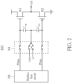
    • FIG. 2 is a diagram illustrating a first phase (e.g., RST mode) of a discrete operation performed at the capacitor weighted segmentation buffer shown in FIG. 1 according to an embodiment of the present invention.
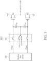
    • FIG. 3 is a diagram illustrating a second phase (e.g., BUFmode) of the discrete operation performed at the capacitor weighted segmentation buffer shown in FIG. 1 according to an embodiment of the present invention.
    • FIG. 4 is a diagram illustrating a first phase (e.g., RST mode) of a discrete operation performed by a first processing circuit with integration of a DAC and a buffer according to an embodiment of the present invention.
    • FIG. 5 is a diagram illustrating a second phase (e.g., BUFmode) of the discrete operation performed by the first processing circuit with integration of the DAC and the buffer according to an embodiment of the present invention.
    • FIG. 6 is a diagram illustrating a first phase (e.g., RST mode) of a discrete operation performed at a second processing circuit with integration of a DAC and a buffer according to an embodiment of the present invention.
    • FIG. 7 is a diagram illustrating a second phase (e.g., BUF mode) of the discrete operation performed at the second processing circuit with integration of the DAC and the buffer according to an embodiment of the present invention.
    • FIG. 8 is a diagram illustrating a first ACIM circuit using a capacitor weighted segmentation buffer as its output buffer according to an embodiment of the present invention.
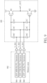
    • FIG. 9 is a diagram illustrating a second ACIM circuit using a capacitor weighted segmentation buffer as its output buffer according to an embodiment of the present invention.
    Detailed Description
  • Certain terms are used throughout the following description and claims, which refer to particular components. As one skilled in the art will appreciate, electronic equipment manufacturers may refer to a component by different names. This document does not intend to distinguish between components that differ in name but not in function. In the following description and in the claims, the terms "include" and "comprise" are used in an open-ended fashion, and thus should be interpreted to mean "include, but not limited to ...". Also, the term "couple" is intended to mean either an indirect or direct electrical connection. Accordingly, if one device is coupled to another device, that connection may be through a direct electrical connection, or through an indirect electrical connection via other devices and connections.
  • FIG. 1 is a diagram illustrating a capacitor weighted segmentation buffer according to an embodiment of the present invention. The capacitor weighted segmentation buffer 100 includes a push-pull buffer circuit 102, a plurality of capacitors C11-C1N and C21-C2N (N ≥ 2), a switch circuit 104, and a replica bias circuit 106. The push-pull buffer circuit 102 includes two transistors M1 and M2. For example, the transistor M2 may be implemented by a P-channel metal-oxide-semiconductor (PMOS) transistor, and the transistor M1 may be implemented by an N-channel metal-oxide-semiconductor (NMOS) transistor. As shown in FIG. 1, the transistor (e.g., NMOS transistor) M1 has a control terminal (e.g., gate terminal) and two connection terminals (e.g., source terminal and drain terminal), where one connection terminal (e.g., drain terminal) is coupled to a reference voltage (e.g., supply voltage VDD), and the other connection terminal (e.g., source terminal) is coupled to an output node N_OUT of the capacitor weighted segmentation buffer 100. In addition, the transistor (e.g., PMOS transistor) M2 has a control terminal (e.g., gate terminal) and two connection terminals (e.g., source terminal and drain terminal), where one connection terminal (e.g., drain terminal) is coupled to another reference voltage (e.g., ground voltage GND), and the other connection terminal (e.g., source terminal) is coupled to the output node N_OUT of the capacitor weighted segmentation buffer 100. In some embodiments of the present invention, the output node N_OUT of the capacitor weighted segmentation buffer 100 is coupled to a following processing stage. In other words, the capacitor weighted segmentation buffer 100 may act as an output buffer or output driver for driving the following processing stage. For example, the following processing stage may be an ACIM circuit.
  • The capacitor C11 has a first terminal (e.g., top plate) coupled to the control terminal of the transistor M1 and a second terminal (e.g., bottom plate) arranged to receive a first input signal V_IN1 of the capacitor weighted segmentation buffer 100. The capacitor C21 has a first terminal (e.g., bottom plate) coupled to the control terminal of the transistor M2 and a second terminal (e.g., top plate) arranged to receive the first input signal V_IN1 of the capacitor weighted segmentation buffer 100. The capacitor C12 has a first terminal (e.g., top plate) coupled to the control terminal of the transistor M1 and a second terminal (e.g., bottom plate) arranged to receive a second input signal V_IN2 of the capacitor weighted segmentation buffer 100. The capacitor C22 has a first terminal (e.g., bottom plate) coupled to the control terminal of the transistor M2 and a second terminal (e.g., top plate) arranged to receive the second input signal V_IN2 of the capacitor weighted segmentation buffer 100. The capacitor C1N has a first terminal (e.g., top plate) coupled to the control terminal of the transistor M1 and a second terminal (e.g., bottom plate) arranged to receive an Nth input signal V_INN of the capacitor weighted segmentation buffer 100. The capacitor C2N has a first terminal (e.g., bottom plate) coupled to the control terminal of the transistor M2 and a second terminal (e.g., top plate) arranged to receive the Nth input signal V_INN of the capacitor weighted segmentation buffer 100.
  • Both of the capacitors C1i and C2i have the same capacitance value CVi, where i = 11, 2, ..., N} . In addition, the capacitance values CV1-CVN include different capacitance values. For example, the capacitance value CV1 is larger than each of the capacitance values CV2 and CVN, and the capacitance value CV2 is larger than the capacitance value CVN. For another example, the capacitors C11, C12, ..., C1N form one binary weighted capacitor array, and the capacitors C21, C22, ..., C2N form another binary weighted capacitor array. However, these are for illustrative purposes only, and are not meant to be limitations of the present invention. In practice, settings of the capacitance values CV1-CVN can be adjusted, depending upon actual design considerations. Furthermore, the number of capacitors C11-C1N and C21-C2N ( N ≥ 2) can be adjusted, depending upon actual design considerations.
  • In this embodiment, the push-pull buffer circuit 102 operates as a discrete-time push-pull buffer. Specifically, the discrete-time operation of the push-pull buffer circuit 102 includes a first phase in which the push-pull buffer circuit 102 operates in a reset (RST) mode and a second phase in which the push-pull buffer circuit 102 operates in a buffer (BUF) mode. The mode switching of the push-pull buffer circuit 102 is controlled by the switch circuit 104 that may be implemented using a plurality of switches. Specifically, the switch circuit 104 is arranged to support two configurations CFG_1 and CFG_2. When the switch circuit 104 is controlled to have the configuration CFG_1 (which is defined by ON/OFF statues of switches in the switch circuit 104), the push-pull buffer circuit 102 operates in the RST mode. When the switch circuit 104 is controlled to have the configuration CFG_2 (which is defined by ON/OFF statues of switches in the switch circuit 104), the push-pull buffer circuit 102 operates in the BUF mode.
  • As shown in FIG. 1, the switch circuit 104 is coupled between the replica bias circuit 106 and the control terminals of the transistors M1 and M2, and is further coupled between a plurality of input nodes N_IN1, N_IN2, ..., N_INN of the capacitor weighted segmentation buffer 100 and the capacitors C11-C1N and C21-C2N, where the input nodes N_IN1-N_INN are arranged to receive the input signals V_IN1-V_INN from a preceding processing stage, respectively. The replica bias circuit 106 is arranged to generate one bias voltage Nbias for the transistor M1 (e.g., NMOS transistor), and generate another bias voltage for the transistor M2 (e.g., PMOS transistor). Please refer to FIG. 2 and FIG. 3. FIG. 2 is a diagram illustrating a first phase (e.g., RST mode) of a discrete operation performed at the capacitor weighted segmentation buffer 100 according to an embodiment of the present invention. FIG. 3 is a diagram illustrating a second phase (e.g., BUF mode) of the discrete operation performed at the capacitor weighted segmentation buffer 100 according to an embodiment of the present invention. For brevity and simplicity, the weighted capacitors C11-C1N ( N ≥ 2) are collectively represented by one capacitor Ctop in FIGs. 2-3, the weighted capacitors C21-C2N ( N ≥ 2) are collectively represented by one capacitor Cbot in FIGs. 2-3, and the input signals V_IN1-V_INN are collectively represented by one input signal (which is an analog input) vi. When the push-pull buffer circuit 102 operates in the RST mode due to the switch circuit 104 with the configuration CFG_1, the replica bias circuit 106 generates and outputs the bias voltage Nbias to the control terminal of the transistor M1, and generates and outputs the bias voltage Pbias to the control terminal of the transistor M2. When the push-pull buffer circuit 102 operates in the BUF mode due to the switch circuit 104 with the configuration CFG_2, the replica bias circuit 106 is disconnected from the push-pull buffer circuit 102. Since the replica bias circuit 106 is used to set the bias voltages Nbias and Pbias of the push-pull buffer circuit 102, the bias voltages Nbias and Pbias are stable across PVT variation, such that the gain of the push-pull buffer circuit 102 will not vary across PVT variation. In other words, with the help of the PVT tracking capability of the replica bias circuit 106, the push-pull buffer circuit 102 has a stable and strong buffering capability across all PVT variations.
  • Furthermore, when the push-pull buffer circuit 102 operates in the RST mode due to the switch circuit 104 with the configuration CFG_1, the input node N_IN1 (particularly, input signal V_IN1 received by input node N_IN1) is disconnected from capacitors C11 and C21, the input node N_IN2 (particularly, input signal V_IN2 received by input node N_IN2) is disconnected from capacitors C12 and C22, and the input node N_INN (particularly, input signal V_INN received by input node N_INN) is disconnected from capacitors C1N and C2N. In addition, a common-mode voltage vcm that acts as a reset voltage is applied to bottom plates of all weighted capacitors C11-C1N and top plates of all weighted capacitors C21-C2N. When the push-pull buffer circuit 102 operates in the BUF mode due to the switch circuit 104 with the configuration CFG_2, the input signal V_IN1 received by the input node N_IN1 is delivered to capacitors C11 and C21 (particularly, bottom plate of capacitor C11 and top plate of capacitor C21), the input signal V_IN2 received by the input node N_IN2 is delivered to capacitors C12 and C22 (particularly, bottom plate of capacitor C12 and top plate of capacitor C22), and the input signal V_INN received by the input node N_INN is delivered to capacitors C1N and C2N (particularly, bottom plate of capacitor C1N and top plate of capacitor C2N).
  • The capacitor weighted segmentation buffer 100 generates an output signal V_OUT (which is an analog output) at the output node N_OUT by combining the input signals V_IN1-V_INN (which are analog inputs) through charge redistribution among the weighted capacitor array C11-C1N and the weighted capacitor array C21-C2N. Hence, the preceding processing stage (which provides the input signals V_IN1-V_INN) can leverage the capacitor weighted segmentation buffer 100 to achieve complexity reduction such as node (energy) reduction. Furthermore, since the push-pull driver circuit 102 is used as a discrete-time buffer rather than a continuous-time buffer, it allows integration of a digital-to-analog converter (DAC) and a buffer. In one exemplary implementation, the capacitor weighted segmentation buffer 100 may be integrated with a DAC to achieve chip area reduction.
  • Please refer to FIG. 4 and FIG. 5. FIG. 4 is a diagram illustrating a first phase (e.g., RST mode) of a discrete operation performed at a first processing circuit with integration of a DAC and a buffer according to an embodiment of the present invention. FIG. 5 is a diagram illustrating a second phase (e.g., BUF mode) of the discrete operation performed at the first processing circuit with integration of the DAC and the buffer according to an embodiment of the present invention. In this embodiment, the processing circuit 400 includes the capacitor weighted segmentation buffer 100 with four capacitors C11=16C, C1N=1C (N=2), C21=16C, and C2N=1C (N=2) . As shown in FIG. 4, when the push-pull buffer circuit 102 operates in the RST mode due to the switch circuit 104 with the configuration CFG_1, the bias voltage Nbias generated from the replica bias circuit 106 is applied to the control terminal of the transistor M1, the bias voltage Pbias generated from the replica bias circuit 106 is applied to the control terminal of the transistor M2, and the common-mode voltage vcm set by V<0> is applied to all capacitors C11=16C, C1N=1C (N=2), C21=16C, and C2N=1C (N=2).
  • The processing circuit 400 employs DAC and buffer integration, and thus further includes a DAC that shares the capacitors C11=16C, C1N=1C (N=2), C21=16C, and C2N=1C (N=2) used by the capacitor weighted segmentation buffer 100. In this embodiment, the DAC includes a resistor digital-to-analog converter (RDAC) 402 and a capacitor digital-to-analog converter (CDAC) 404, where the capacitors C11=16C, C1N=1C (N=2), C21=16C, and C2N=1C (N=2) are used by the CDAC 404. For a particular application such as an artificial intelligence (AI) application, multiple processing circuits 400 may be used to provide multiple AI inputs to a following processing stage such as an ACIM circuit for analog computation of convolutions. In some embodiments of the present invention, the RDAC 402 used by one processing circuit 400 may be shared by other processing circuits 400 for hardware and cost reduction. However, this is for illustrative purposes only, and is not meant to be a limitation of the present invention.
  • As shown in FIG. 5, when the push-pull buffer circuit 102 operates in the BUF mode due to the switch circuit 104 with the configuration CFG_2, the input signals V_IN1 and V_IN2 (i.e., V_INN with N=2) generated by the DAC (which includes RDAC 402 and CDAC 404) are delivered to the capacitors C11=16C, C1N=1C (N=2), C21=16C, and C2N=1C (N=2). Suppose that a digital code DA_Vin of the DAC (which includes RDAC 402 and CDAC 404) has 8 bits. For example, the digital code DA_Vin<7:0> may be one input data of a neural network used by an AI application. In this embodiment, the digital code DA_Vin<7:0> is divided into two 4-bit (4b) segments, including a most significant bit (MSB) segment DA_Vin<7:4> and a least significant bit (LSB) segment DA_Vin<3:0>. Hence, the RDAC 402 is implemented using a 4b RDAC that is arranged to provide a plurality of reference voltage levels V<15:0>. The CDAC 404 includes two 4b decoders 406 and 408. The 4b decoder 406 acts as a multiplexer, and is arranged to select and output one of the reference voltage levels V<15:0> as the input signal V_IN1 according to the MSB segment DA_Vin<7:4>, where the input signal V_IN1 is applied to the bottom plate of the capacitor C11=16C and the top plate of the capacitor C21=16C. The 4b decoder 408 acts as a multiplexer, and is arranged to select and output one of the reference voltage levels V<15:0> as the input signal V_IN2 (i.e., V_INN with N=2) according to the LSB segment DA_Vin<3:0>, where the input signal V_IN2 (i.e., V_INN with N=2) is applied to the bottom plate of the capacitor C1N=1C (N=2) and the top plate of the capacitor C2N=1C (N=2).
  • The segmentation design shown in FIG. 4 and FIG. 5 is for illustrative purposes only, and is not meant to be a limitation of the present invention. In practice, the segmentation design may be adjusted, depending upon actual design considerations.
  • Please refer to FIG. 6 and FIG. 7. FIG. 6 is a diagram illustrating a first phase (e.g., RST mode) of a discrete operation performed at a second processing circuit with integration of a DAC and a buffer according to an embodiment of the present invention. FIG. 7 is a diagram illustrating a second phase (e.g., BUF mode) of the discrete operation performed at the second processing circuit with integration of the DAC and the buffer according to an embodiment of the present invention. In this embodiment, the processing circuit 600 includes the capacitor weighted segmentation buffer 100 with six capacitors C11=16C, C12=4C, C1N=1C (N=3), C21=16C, C22=4C, and C2N=1C (N=3). As shown in FIG. 6, when the push-pull buffer circuit 102 operates in the RST mode due to the switch circuit 104 with the configuration CFG_1, the bias voltage Nbias generated from the replica bias circuit 106 is applied to the control terminal of the transistor M1, the bias voltage Pbias generated from the replica bias circuit 106 is applied to the control terminal of the transistor M2, and the common-mode voltage vcm set by V<0> is applied to capacitors C11=16C, C12=4C, C1N=1C (N=3), C21=16C, C22=4C, and C2N=1C (N=3).
  • The processing circuit 600 employs DAC and buffer integration, and thus further includes a DAC that shares the capacitors C11=16C, C12=4C, C1N=1C (N=3), C21=16C, C22=4C, and C2N=1C (N=3) used by the capacitor weighted segmentation buffer 100. In this embodiment, the DAC includes an RDAC 602 and a CDAC 604, where the capacitors C11=16C, C12=4C, C1N=1C (N=3), C21=16C, C22=4C, and C2N=1C (N=3) are used by the CDAC 604. For a particular application such as an AI application, multiple processing circuits 600 may be used to provide multiple AI inputs to a following processing stage such as an ACIM circuit. Hence, the RDAC 602 used by one processing circuit 600 may be shared by other processing circuits 600 for hardware and cost reduction. However, this is for illustrative purposes only, and is not meant to be a limitation of the present invention.
  • As shown in FIG. 7, when the push-pull buffer circuit 102 operates in the BUF mode due to the switch circuit 104 with the configuration CFG_2, the input signals V_IN1, V_IN2, and V_IN3 (i.e., V_INN with N=3) generated by the DAC (which includes RDAC 602 and CDAC 604) are delivered to the capacitors C11=16C, C12=4C, C1N=1C (N=3), C21=16C, C22=4C, and C2N=1C (N=3) . Suppose that a digital code DA_Vin of the DAC (which includes RDAC 402 and CDAC 404) has 6 bits. For example, the digital code DA_Vin<5:0> may be one input data of a neural network used by an AI application. In this embodiment, the digital code DA_Vin<5:0> is divided into three 2-bit (2b) segments, including an MSB segment DA_Vin<5:4>, a center significant bit (CSB) segment DA_Vin<3:2>, and an LSB segment DA_Vin<1:0>. Hence, the RDAC 602 is implemented using a 2b RDAC that is arranged to provide a plurality of reference voltage levels V<3:0>. The CDAC 604 includes three 2b decoders 606, 608, and 610. The 2b decoder 606 acts as a multiplexer, and is arranged to select and output one of the reference voltage levels V<3:0> as the input signal V_IN1 according to the MSB segment DA_Vin<5:4>, where the input signal V_IN1 is applied to the bottom plate of the capacitor C11=16C and the top plate of the capacitor C21=16C. The 4b decoder 608 acts as a multiplexer, and is arranged to select and output one of the reference voltage levels V<3:0> as the input signal V_IN2 according to the CSB segment DA_Vin<3:2>, where the input signal V_IN2 is applied to the bottom plate of the capacitor C12=4C and the top plate of the capacitor C22=4C. The 4b decoder 410 acts as a multiplexer, and is arranged to select and output one of the reference voltage levels V<3:0> as the input signal V_IN3 (i.e., V_INN with N=3) according to the LSB segment DA_Vin<1:0>, where the input signal V_IN3 (i.e., V_INN with N=3) is applied to the bottom plate of the capacitor C1N=1C (N=3) and the top plate of the capacitor C2N=1C (N=3).
  • In summary, the processing circuit 400/600 with integration of a DAC and a buffer uses the push-pull buffer circuit 102 biased by the replica bias circuit 106 that has a stable and strong buffering/driving capability across all PVT variations, uses accurate RDAC 402/602 and CDAC 404/604 that provide a high DAC resolution, and uses a proper segmentation for node (energy) reduction. Compared to a conventional DAC that requires 28 nodes to provide 28 voltage levels for selection, the DAC consisting of RDAC 402/602 and CDAC 406/606 requires a fewer number of nodes, and thus occupies a smaller chip area.
  • In another exemplary implementation, the capacitor weighted segmentation buffer 100 may be used as an ACIM buffer. FIG. 8 is a diagram illustrating a first ACIM circuit using a capacitor weighted segmentation buffer as its output buffer according to an embodiment of the present invention. In this embodiment, an ACIM circuit is implemented using a memory array 802. For example, the ACIM circuit is a static random access memory (SRAM)-based CIM circuit that performs the multiplication and accumulation (MAC) operations in an analog manner. In this embodiment, the capacitor weighted segmentation buffer 100 has four capacitors C11=16C, C1N=1C (N=2), C21=16C, and C2N=1C (N=2). When the push-pull buffer circuit 102 operates in the RST mode due to the switch circuit 104 with the configuration CFG_1, the bias voltage Nbias generated from the replica bias circuit 106 is applied to the control terminal of the transistor M1, the bias voltage Pbias generated from the replica bias circuit 106 is applied to the control terminal of the transistor M2, and the common-mode voltage vcm is applied to capacitors C11=16C, C1N=1C (N=2), C21=16C, and C2N=1C (N=2).
  • When the push-pull buffer circuit 102 operates in the BUF mode due to the switch circuit 104 with the configuration CFG_2, the input voltages V_IN1 and V_IN2 (i.e., V_INN with N=2) are delivered to the capacitors C11=16C, C1N=1C (N=2), C21=16C, and C2N=1C (N=2) . As shown in FIG. 8, the input voltages V_IN1 and V_IN2 (i.e., V_INN with N=2) are generated from the ACIM circuit implemented using the memory array 802. Suppose that the ACIM circuit is used for an AI application to deal with MAC operations. Hence, each of the input voltages V_IN1 and V_IN2 (i.e., V_INN with N=2) corresponds to one input data of a neural network used by an AP application. For example, the AI input includes 64 8b input data IN1[7:0]-IN64[7:0], and are converted into analog inputs, for example, by 64 processing circuits 400/600, respectively. The memory array 802 stores 64 8b weights W1[7:0]-W64[7:0], and receives the analog inputs representative of 8b input data IN1[7:0]-IN64[7:0]. It is difficult for an ACIM circuit to achieve multiplication and accumulation based on 8b input data and 8b weight. To reduce the complexity, each of the 8b weights W2[7:0]-W64[7:0] is divided into an MSB segment W[7:4] and an LSB segment W[3:0], and the ACIM circuit includes two processing circuits (e.g., SRAM-based CIM circuits) 804 and 806. The processing circuit 804 is arranged to deal with a 4b weight (4bW) MSB bit line/word line (BL/WL) operation. Hence, the processing circuit 804 generates and outputs the input signal V_IN1 to the capacitor weighted segmentation buffer (which acts as an ACIM buffer) 100 according to the analog inputs representative of 8b input data IN1[7:0]-IN64[7:0] and MSB segments W1[7:4]- We4[7:4] of stored 8b weights W1[7:0]- W64[7:0]. The processing circuit 806 is arranged to deal with a 4b weight (4bW) LSB BL/WL operation. Hence, the processing circuit 806 generates and outputs the input signal V_IN2 (i.e., V_INN with N=2) to the capacitor weighted segmentation buffer (which acts as an ACIM buffer) 100 according to the analog inputs representative of 8b input data IN1[7:0]-IN64[7:0] and LSB segments W1[3:0]- W64[3:0] of stored 8b weights W1[7:0]- W64[7:0]. The generation of the input signals V_IN1 and V_IN2 (i.e., V_INN with N=2) can be simply expressed using the following formulas. V _ IN 1 = k = 1 64 IN k 7 : 0 W k 7 : 4
    Figure imgb0001
    V _ IN 2 = k = 1 64 IN k 7 : 0 W k 3 : 0
    Figure imgb0002
  • The capacitor weighted segmentation buffer 100 generates the output signal V_OUT (which is an analog output of k = 1 64 IN k 7 : 0 W k 7 : 0
    Figure imgb0003
    ) by combining the input signals V_IN1 and V_IN2 (i.e., V_INN with N=2) through charge redistribution among the weighted capacitor array C11=16C, C1N=1C (N=2) and the weighted capacitor array C21=16C, C2N=1C (N=2) .
  • The segmentation design shown in FIG. 8 is for illustrative purposes only, and is not meant to be a limitation of the present invention. In practice, the segmentation design may be adjusted, depending upon actual design considerations. FIG. 9 is a diagram illustrating a second ACIM circuit using a capacitor weighted segmentation buffer as its output buffer according to an embodiment of the present invention. In this embodiment, an ACIM circuit is implemented using a memory array 902. For example, the ACIM circuit is an SRAM-based CIM circuit that performs the MAC operations in an analog manner. In this embodiment, the capacitor weighted segmentation buffer 100 has six capacitors C11=16C, C12=4C, C1N=1C (N=3), C21=16C, C22=4C, and C2N=1C (N=3) . When the push-pull buffer circuit 102 operates in the RST mode due to the switch circuit 104 with the configuration CFG_1, the bias voltage Nbias generated from the replica bias circuit 106 is applied to the control terminal of the transistor M1, the bias voltage Pbias generated from the replica bias circuit 106 is applied to the control terminal of the transistor M2, and the common-mode voltage vcm is applied to capacitors C11=16C, C12=4C, C1N=1C (N=3), C21=16C, C22=4C, and C2N=1C (N=3).
  • When the push-pull buffer circuit 102 operates in the BUF mode due to the switch circuit 104 with the configuration CFG_2, the input voltages V_IN1, V_IN2 and V_IN3 (i.e., V_INN with N=3) are delivered to the capacitors C11=16C, C12=4C, C1N=1C (N=3), C21=16C, C22=4C, and C2N=1C (N=3). As shown in FIG. 9, the input voltages V_IN1, V_IN2, and V_IN3 (i.e., V_INN with N=3) are generated from the ACIM circuit implemented using the memory array 902. Suppose that the ACIM circuit is used for an AI application to deal with MAC operations. Hence, each of the input voltages V_IN1, V_IN2, and V_IN3 (i.e., V_INN with N=3) corresponds to one input data of a neural network used by an AP application. For example, the AI input includes 64 8b input data IN1[7:0]-IN64[7:0], and are converted into analog inputs, for example, by 64 processing circuits 400/600, respectively. The memory array 902 stores 64 6b weights W1[5:0]- We4[5:0], and receives the analog inputs representative of 8b input data IN1[7:0]-IN64[7:0]. To reduce the complexity, each of the 6b weights W1[5:0]- W64[5:0] is divided into an MSB segment W[5:4], a CSB segment W[3:2], and an LSB segment W[1:0], and the ACIM circuit includes three processing circuits (e.g., SRAM-based CIM circuits) 904, 906, and 908. The processing circuit 902 is arranged to deal with a 2b weight (2bW) MSB BL/WL operation. Hence, the processing circuit 904 generates and outputs the input signal V_IN1 to the capacitor weighted segmentation buffer (which acts as an ACIM buffer) 100 according to the analog inputs representative of 8b input data IN1[7:0]-IN64[7:0] and MSB segments W1[5:4]- W64[5:4] of stored 6b weights W1[5:0]- W64[5:0]. The processing circuit 904 is arranged to deal with a 2b weight (2bW) CSB BL/WL operation. Hence, the processing circuit 906 generates and outputs the input signal V_IN2 to the capacitor weighted segmentation buffer (which acts as an ACIM buffer) 100 according to the analog inputs representative of 8b input data IN1[7:0]-IN64[7:0] and CSB segments W1[3:2]- W64[3:2] of stored 6b weights W1[5:0]- W64[5:0]. The processing circuit 908 is arranged to deal with a 2b weight (2bW) LSB BL/WL operation. Hence, the processing circuit 908 generates and outputs the input signal V_IN3 (i.e., V_INN with N=3) to the capacitor weighted segmentation buffer (which acts as an ACIM buffer) 100 according to the analog inputs representative of 8b input data IN1[7:0]-IN64[7:0] and LSB segments W1[1:0]- W64[1:0] of stored 6b weights W1[5:0]- W64[5:0]. The generation of the input signals V_IN1, V_IN2, and V_IN3 (i.e., V_INN with N=3) can be simply expressed using the following formulas. V _ IN 1 = k = 1 64 IN k 7 : 0 W k 5 : 4
    Figure imgb0004
    V _ IN 2 = k = 1 64 IN k 7 : 0 W k 3 : 2
    Figure imgb0005
    V _ IN 3 = k = 1 64 IN k 7 : 0 W k 1 : 0
    Figure imgb0006
  • The capacitor weighted segmentation buffer 100 generates the output signal V_OUT (which is an analog output of k = 1 64 IN k 7 : 0 W k 5 : 0
    Figure imgb0007
    ) by combining the input signals V_IN1, V_IN2, and V_IN3 (i.e., V_INN with N=3) through charge redistribution among the weighted capacitor array C11=16C, C12=4C, C1N=1C (N=3) and the weighted capacitor array C21=16C, C22=4C, and C2N=1C (N=3).
  • In summary, regarding an ACM circuit using the capacitor weighted segmentation buffer 100 as its output buffer, the push-pull buffer circuit 102 biased by the replica bias circuit 106 can offer a stable and strong buffering/driving capability across all PVT variations, the weighted capacitors have accurate capacitance ratios for recombination of input signals, and a proper segmentation of weights leads to node (energy) reduction as well as chip area reduction.
  • Those skilled in the art will readily observe that numerous modifications and alterations of the device and method may be made while retaining the teachings of the invention. Accordingly, the above disclosure should be construed as limited only by the metes and bounds of the appended claims.
  • The present invention may also be defined by the following numbered clauses.
    1. 1. A capacitor weighted segmentation buffer comprising:
      • a push-pull buffer circuit, comprising:
        • a first transistor, having a control terminal, a first connection terminal, and a second connection terminal; and
        • a second transistor, having a control terminal, a first connection terminal, and a second connection terminal, wherein the second connection terminal of the first transistor and the second connection terminal of the second transistor are coupled to an output node of the capacitor weighted segmentation buffer; and
      • a plurality of capacitors, comprising:
        • a first capacitor, having a first terminal coupled to the control terminal of the first transistor, and a second terminal arranged to receive a first input signal of the capacitor weighted segmentation buffer;
        • a second capacitor, having a first terminal coupled to the control terminal of the second transistor, and a second terminal arranged to receive the first input signal of the capacitor weighted segmentation buffer;
        • a third capacitor, having a first terminal coupled to the control terminal of the first transistor, and a second terminal arranged to receive a second input signal of the capacitor weighted segmentation buffer; and
        • a fourth capacitor, having a first terminal coupled to the control terminal of the second transistor, and a second terminal arranged to receive the second input signal of the capacitor weighted segmentation buffer;
      • wherein each of the first capacitor and the second capacitor has a first capacitance value, and each of the third capacitor and the fourth capacitor has a second capacitance value different from the first capacitance value.
    2. 2. The capacitor weighted segmentation buffer of clause 1, wherein the plurality of capacitors further comprise:
      • a fifth capacitor, having a first terminal coupled to the control terminal of the first transistor, and a second terminal arranged to receive a third input signal of the capacitor weighted segmentation buffer; and
      • a sixth capacitor, having a first terminal coupled to the control terminal of the second transistor, and a second terminal arranged to receive the third input signal of the capacitor weighted segmentation buffer;
      • wherein each of the fifth capacitor and the sixth capacitor has a third capacitance value different from any of the first capacitance value and the second capacitance value.
    3. 3. The capacitor weighted segmentation buffer of clause 1, further comprising:
      a switch circuit, arranged to support a first configuration and a second configuration, wherein the push-pull buffer circuit operates in a reset mode when the switch circuit has the first configuration, and operates in a buffer mode when the switch circuit has the second configuration.
    4. 4. The capacitor weighted segmentation buffer of clause 3, further comprising:
      a replica bias circuit, arranged to generate and output a first bias voltage to the control terminal of the first transistor and generate and output a second bias voltage to the control terminal of the second transistor when the push-pull buffer circuit operates in the reset mode.
    5. 5. The capacitor weighted segmentation buffer of clause 4, wherein the replica bias circuit is disconnected from the push-pull buffer circuit when the push-pull buffer circuit operates in the buffer mode.
    6. 6. The capacitor weighted segmentation buffer of clause 3, wherein the first input signal is delivered to the second terminal of the first capacitor and the second terminal of the third capacitor when the push-pull buffer circuit operates in the buffer mode; and the second input signal is delivered to the second terminal of the second capacitor and the second terminal of the fourth capacitor when the push-pull buffer circuit operates in the buffer mode.
    7. 7. The capacitor weighted segmentation buffer of clause 6, wherein the first input signal is disconnected from the first capacitor and the third capacitor and the second input signal is disconnected from the second capacitor and the fourth capacitor when the push-pull buffer circuit operates in the reset mode.
    8. 8. The capacitor weighted segmentation buffer of clause 3, wherein a common-mode voltage is delivered to the second terminal of the first capacitor, the second terminal of the second capacitor, the second terminal of the third capacitor and the second terminal of the fourth capacitor when the push-pull buffer circuit operates in the reset mode.
    9. 9. The capacitor weighted segmentation buffer of clause 1, wherein the capacitor weighted segmentation buffer is integrated with a digital-to-analog converter (DAC).
    10. 10. The capacitor weighted segmentation buffer of clause 9, wherein the DAC comprises:
      • a resistor digital-to-analog converter (RDAC), arranged to provide a plurality of reference voltage levels; and
      • a capacitor digital-to-analog converter (CDAC), wherein the plurality of capacitors are used by the CDAC, and the plurality of reference voltage levels are provided to the CDAC.
    11. 11. The capacitor weighted segmentation buffer of clause 10, wherein the CDAC comprises:
      • the first capacitor;
      • the third capacitor;
      • the second capacitor;
      • the fourth capacitor;
      • a first decoder, arranged to select and output one of the plurality of reference voltage levels as the first input signal according to a first segment of a digital code of the DAC; and
      • a second decoder, arranged to select and output one of the plurality of reference voltage levels as the second input signal according to a second segment of the digital code of the DAC.
    12. 12. The capacitor weighted segmentation buffer of clause 11, wherein the digital code is one input data of a neural network.
    13. 13. The capacitor weighted segmentation buffer of clause 9, wherein the output node of the capacitor weighted segmentation buffer is coupled to an analog compute-in-memory (ACIM) circuit.
    14. 14. The capacitor weighted segmentation buffer of clause 1, wherein the capacitor weighted segmentation buffer is an analog compute-in-memory (ACIM) buffer.
    15. 15. The capacitor weighted segmentation buffer of clause 14, wherein each of the first input signal and the second input signal is generated from an ACIM circuit, and the ACIM circuit comprises:
      a plurality of processing circuits, comprising:
      • a first processing circuit, arranged to generate and output the first input signal according to a plurality of analog inputs and first segments of a plurality of stored data; and
      • a second processing circuit, arranged to generate and output the second input signal according to the plurality of analog inputs and second segments of the plurality of stored data.
    16. 16. The capacitor weighted segmentation buffer of clause 15, wherein each of the plurality of processing circuits is a multiply-accumulate (MAC) circuit.
    17. 17. The capacitor weighted segmentation buffer of clause 15, wherein each of the analog inputs corresponds to one input data of a neural network.

Claims (15)

  1. A capacitor weighted segmentation buffer (100) comprising:
    a push-pull buffer circuit (102), comprising:
    a first transistor, having a control terminal, a first connection terminal, and a second connection terminal; and
    a second transistor, having a control terminal, a first connection terminal, and a second connection terminal, wherein the second connection terminal of the first transistor and the second connection terminal of the second transistor are coupled to an output node of the capacitor weighted segmentation buffer (100); and
    a plurality of capacitors, comprising:
    a first capacitor, having a first terminal coupled to the control terminal of the first transistor, and a second terminal arranged to receive a first input signal of the capacitor weighted segmentation buffer (100);
    a second capacitor, having a first terminal coupled to the control terminal of the second transistor, and a second terminal arranged to receive the first input signal of the capacitor weighted segmentation buffer (100);
    a third capacitor, having a first terminal coupled to the control terminal of the first transistor, and a second terminal arranged to receive a second input signal of the capacitor weighted segmentation buffer (100); and
    a fourth capacitor, having a first terminal coupled to the control terminal of the second transistor, and a second terminal arranged to receive the second input signal of the capacitor weighted segmentation buffer (100);
    wherein each of the first capacitor and the second capacitor has a first capacitance value, and each of the third capacitor and the fourth capacitor has a second capacitance value different from the first capacitance value.
  2. The capacitor weighted segmentation buffer (100) of claim 1, wherein the plurality of capacitors further comprise:
    a fifth capacitor, having a first terminal coupled to the control terminal of the first transistor, and a second terminal arranged to receive a third input signal of the capacitor weighted segmentation buffer (100); and
    a sixth capacitor, having a first terminal coupled to the control terminal of the second transistor, and a second terminal arranged to receive the third input signal of the capacitor weighted segmentation buffer (100);
    wherein each of the fifth capacitor and the sixth capacitor has a third capacitance value different from any of the first capacitance value and the second capacitance value.
  3. The capacitor weighted segmentation buffer (100) of claim 1, further comprising:
    a switch circuit (104), arranged to support a first configuration and a second configuration, wherein the push-pull buffer circuit (102) operates in a reset mode when the switch circuit (104) has the first configuration, and operates in a buffer mode when the switch circuit (104) has the second configuration.
  4. The capacitor weighted segmentation buffer (100) of claim 3, further comprising:
    a replica bias circuit (106), arranged to generate and output a first bias voltage to the control terminal of the first transistor and generate and output a second bias voltage to the control terminal of the second transistor when the push-pull buffer circuit (102) operates in the reset mode.
  5. The capacitor weighted segmentation buffer (100) of claim 4, wherein the replica bias circuit (106) is disconnected from the push-pull buffer circuit (102) when the push-pull buffer circuit (102) operates in the buffer mode.
  6. The capacitor weighted segmentation buffer (100) of claim 3, wherein the first input signal is delivered to the second terminal of the first capacitor and the second terminal of the third capacitor when the push-pull buffer circuit (102) operates in the buffer mode; and the second input signal is delivered to the second terminal of the second capacitor and the second terminal of the fourth capacitor when the push-pull buffer circuit (102) operates in the buffer mode.
  7. The capacitor weighted segmentation buffer (100) of claim 6, wherein the first input signal is disconnected from the first capacitor and the third capacitor and the second input signal is disconnected from the second capacitor and the fourth capacitor when the push-pull buffer circuit (102) operates in the reset mode.
  8. The capacitor weighted segmentation buffer (100) of claim 3, wherein a common-mode voltage is delivered to the second terminal of the first capacitor, the second terminal of the second capacitor, the second terminal of the third capacitor and the second terminal of the fourth capacitor when the push-pull buffer circuit (102) operates in the reset mode.
  9. The capacitor weighted segmentation buffer (100) of claim 1, wherein the capacitor weighted segmentation buffer (100) is integrated with a digital-to-analog converter, DAC.
  10. The capacitor weighted segmentation buffer (100) of claim 9, wherein the DAC comprises:
    a resistor digital-to-analog converter, RDAC, (402, 602), arranged to provide a plurality of reference voltage levels; and
    a capacitor digital-to-analog converter, CDAC, (404, 604), wherein the plurality of capacitors are used by the CDAC (404, 604), and the plurality of reference voltage levels are provided to the CDAC (404, 604).
  11. The capacitor weighted segmentation buffer (100) of claim 10, wherein the CDAC (404, 604) comprises:
    the first capacitor;
    the third capacitor;
    the second capacitor;
    the fourth capacitor;
    a first decoder (406, 408, 410, 606, 608), arranged to select and output one of the plurality of reference voltage levels as the first input signal according to a first segment of a digital code of the DAC; and
    a second decoder (406, 408, 410, 606, 608), arranged to select and output one of the plurality of reference voltage levels as the second input signal according to a second segment of the digital code of the DAC.
  12. The capacitor weighted segmentation buffer (100) of claim 9, wherein the output node of the capacitor weighted segmentation buffer (100) is coupled to an analog compute-in-memory, ACIM, circuit.
  13. The capacitor weighted segmentation buffer (100) of claim 1, wherein each of the first input signal and the second input signal is generated from an ACIM circuit, and the ACIM circuit comprises:
    a plurality of processing circuits (400, 600, 804, 806, 904, 908), comprising:
    a first processing circuit (400, 600, 804, 806, 904, 908), arranged to generate and output the first input signal according to a plurality of analog inputs and first segments of a plurality of stored data; and
    a second processing circuit (400, 600, 804, 806, 904, 908), arranged to generate and output the second input signal according to the plurality of analog inputs and second segments of the plurality of stored data.
  14. The capacitor weighted segmentation buffer (100) of claim 13, wherein each of the plurality of processing circuits (400, 600, 804, 806, 904, 908) is a multiply-accumulate, MAC, circuit.
  15. The capacitor weighted segmentation buffer (100) of claim 13, wherein each of the analog inputs corresponds to one input data of a neural network.
EP23181176.1A 2022-07-28 2023-06-23 Capacitor weighted segmentation buffer Pending EP4312367A1 (en)

Applications Claiming Priority (4)

Application Number Priority Date Filing Date Title
US202263369674P 2022-07-28 2022-07-28
US202263369673P 2022-07-28 2022-07-28
US202263376125P 2022-09-19 2022-09-19
US18/208,878 US12418297B2 (en) 2022-07-28 2023-06-12 Capacitor weighted segmentation buffer

Publications (1)

Publication Number Publication Date
EP4312367A1 true EP4312367A1 (en) 2024-01-31

Family

ID=87047740

Family Applications (1)

Application Number Title Priority Date Filing Date
EP23181176.1A Pending EP4312367A1 (en) 2022-07-28 2023-06-23 Capacitor weighted segmentation buffer

Country Status (2)

Country Link
US (1) US12418297B2 (en)
EP (1) EP4312367A1 (en)

Citations (2)

* Cited by examiner, † Cited by third party
Publication number Priority date Publication date Assignee Title
US20090185406A1 (en) * 2008-01-22 2009-07-23 Masayuki Uno Switched-Capacitor Circuit Having Two Feedback Capacitors
US20210295905A1 (en) * 2018-06-18 2021-09-23 The Trustees Of Princeton University Efficient reset and evaluation operation of multiplying bit-cells for in-memory computing

Family Cites Families (16)

* Cited by examiner, † Cited by third party
Publication number Priority date Publication date Assignee Title
JPS60100807A (en) * 1983-11-08 1985-06-04 Nec Corp Operational amplifier
US6144331A (en) * 1998-04-08 2000-11-07 Texas Instruments Incorporated Analog to digital converter with a differential output resistor-digital-to-analog-converter for improved noise reduction
US7221921B2 (en) * 1998-05-29 2007-05-22 Silicon Laboratories Partitioning of radio-frequency apparatus
US6778009B1 (en) * 2002-10-31 2004-08-17 National Semiconductor Corporation High gain and wide bandwidth switched capacitor amplifier having a dynamically loaded amplifier output
US6958651B2 (en) * 2002-12-03 2005-10-25 Semiconductor Energy Laboratory Co., Ltd. Analog circuit and display device using the same
KR101368785B1 (en) * 2007-12-29 2014-03-04 삼성전자주식회사 Dual data rate Common Mode Feed-Back circuit and Programmable gain amplifier and Image sensor having the same
US8130133B2 (en) * 2010-07-27 2012-03-06 Linear Technology Corporation A/D converter using isolation switches
EP3576301B1 (en) * 2013-03-15 2024-02-28 Hae-Seung Lee Buffer amplifier circuit
US9455731B1 (en) * 2015-08-05 2016-09-27 Analog Devices Global Digital-to-analog converter with digital charge sharing components
CN110557118B (en) * 2018-05-31 2022-12-27 华为技术有限公司 Phase locking device and phase locking method
US10833685B1 (en) * 2019-06-19 2020-11-10 International Business Machines Corporation Linearized wide tuning range oscillator using magnetic balun/transformer
CN115461712A (en) 2020-02-05 2022-12-09 普林斯顿大学理事会 Scalable array architecture for in-memory computation
US11043948B1 (en) * 2020-02-27 2021-06-22 Qualcomm Incorporated Bandwidth enhanced amplifier for high frequency CML to CMOS conversion
US12242949B2 (en) * 2021-03-29 2025-03-04 Infineon Technologies LLC Compute-in-memory devices, systems and methods of operation thereof
US11705171B2 (en) 2021-09-23 2023-07-18 Intel Corporation Switched capacitor multiplier for compute in-memory applications
US12602200B2 (en) 2021-09-24 2026-04-14 Intel Corporation Analog multiply-accumulate unit for multibit in-memory cell computing

Patent Citations (2)

* Cited by examiner, † Cited by third party
Publication number Priority date Publication date Assignee Title
US20090185406A1 (en) * 2008-01-22 2009-07-23 Masayuki Uno Switched-Capacitor Circuit Having Two Feedback Capacitors
US20210295905A1 (en) * 2018-06-18 2021-09-23 The Trustees Of Princeton University Efficient reset and evaluation operation of multiplying bit-cells for in-memory computing

Non-Patent Citations (2)

* Cited by examiner, † Cited by third party
Title
HSIEH SUNG-EN ET AL: "7.6 A 70.85-86.27TOPS/W PVT-Insensitive 8b Word-Wise ACIM with Post-Processing Relaxation", 2023 IEEE INTERNATIONAL SOLID- STATE CIRCUITS CONFERENCE (ISSCC), IEEE, 19 February 2023 (2023-02-19), pages 136 - 138, XP034314958, DOI: 10.1109/ISSCC42615.2023.10067335 *
JIA HONGYANG ET AL: "Scalable and Programmable Neural Network Inference Accelerator Based on In-Memory Computing", IEEE JOURNAL OF SOLID-STATE CIRCUITS, vol. 57, no. 1, 1 January 2022 (2022-01-01), USA, pages 198 - 211, XP093051677, ISSN: 0018-9200, Retrieved from the Internet <URL:https://ieeexplore.ieee.org/stampPDF/getPDF.jsp?tp=&arnumber=9580448&ref=> DOI: 10.1109/JSSC.2021.3119018 *

Also Published As

Publication number Publication date
US20240039546A1 (en) 2024-02-01
US12418297B2 (en) 2025-09-16

Similar Documents

Publication Publication Date Title
CN103518327B (en) The digital to analog converter of self-timing
EP0537304B1 (en) Analog to digital converter
US8692582B1 (en) Latched comparator circuitry
US7511465B2 (en) Digital pulse width modulated power supply with variable LSB
US5404143A (en) Network swappers and circuits constructed from same
WO2010050293A1 (en) Successive approximation type a/d converter circuit
US6876318B2 (en) Method for increasing rate at which a comparator in a metastable condition transitions to a steady state
US7061421B1 (en) Flash ADC with variable LSB
US20080143391A1 (en) High Speed Latch Comparators
CN107104669B (en) Integrated circuit, method and system for sampling voltage
EP4312217A1 (en) Compute-in-memory circuit with charge-domain passive summation and associated method
US12418297B2 (en) Capacitor weighted segmentation buffer
US6738001B2 (en) Semiconductor integrated circuit
CN117478144A (en) Capacitor Weighted Segmented Buffer
CN108471312A (en) Digital-to-analog converter
US10411726B2 (en) Quantizer including capacitors and operating method of quantizer
JP2004260263A (en) AD converter
US6037885A (en) Digital/analog converter using a floating gate MOS neuron transistor with capacitive coupling
CN117476060A (en) Storage and calculation integrated circuit with charge domain passive summation circuit and related methods
CN116594279B (en) High-speed time-to-digital converter based on nested time amplification and automatic calibration technology
US10886935B2 (en) SAR-DAC device and method for operating an SAR-DAC device
JP2024174731A (en) Semiconductor integrated circuit equipped with MOS switch
JP4687951B2 (en) Programmable delay generator
JP2025064448A (en) Semiconductor Device
CN114301462A (en) Successive approximation type analog-to-digital converter and switch control method

Legal Events

Date Code Title Description
PUAI Public reference made under article 153(3) epc to a published international application that has entered the european phase

Free format text: ORIGINAL CODE: 0009012

STAA Information on the status of an ep patent application or granted ep patent

Free format text: STATUS: THE APPLICATION HAS BEEN PUBLISHED

AK Designated contracting states

Kind code of ref document: A1

Designated state(s): AL AT BE BG CH CY CZ DE DK EE ES FI FR GB GR HR HU IE IS IT LI LT LU LV MC ME MK MT NL NO PL PT RO RS SE SI SK SM TR

STAA Information on the status of an ep patent application or granted ep patent

Free format text: STATUS: REQUEST FOR EXAMINATION WAS MADE

17P Request for examination filed

Effective date: 20240726

RBV Designated contracting states (corrected)

Designated state(s): AL AT BE BG CH CY CZ DE DK EE ES FI FR GB GR HR HU IE IS IT LI LT LU LV MC ME MK MT NL NO PL PT RO RS SE SI SK SM TR