EP4312358A1 - Monitoring device for a power converter, associated monitoring system, power supply system and method - Google Patents
Monitoring device for a power converter, associated monitoring system, power supply system and method Download PDFInfo
- Publication number
- EP4312358A1 EP4312358A1 EP22187270.8A EP22187270A EP4312358A1 EP 4312358 A1 EP4312358 A1 EP 4312358A1 EP 22187270 A EP22187270 A EP 22187270A EP 4312358 A1 EP4312358 A1 EP 4312358A1
- Authority
- EP
- European Patent Office
- Prior art keywords
- signal
- control signal
- variable
- control
- power converter
- Prior art date
- Legal status (The legal status is an assumption and is not a legal conclusion. Google has not performed a legal analysis and makes no representation as to the accuracy of the status listed.)
- Pending
Links
- 238000012806 monitoring device Methods 0.000 title claims abstract description 63
- 238000012544 monitoring process Methods 0.000 title claims abstract description 61
- 238000000034 method Methods 0.000 title claims description 13
- 230000005540 biological transmission Effects 0.000 claims abstract description 19
- 238000005070 sampling Methods 0.000 claims description 2
- 239000013307 optical fiber Substances 0.000 description 2
- 230000006399 behavior Effects 0.000 description 1
- 230000015556 catabolic process Effects 0.000 description 1
- 230000003111 delayed effect Effects 0.000 description 1
- 230000005669 field effect Effects 0.000 description 1
- 229910044991 metal oxide Inorganic materials 0.000 description 1
- 150000004706 metal oxides Chemical class 0.000 description 1
- 230000003287 optical effect Effects 0.000 description 1
- 239000004065 semiconductor Substances 0.000 description 1
Images


Classifications
-
- H—ELECTRICITY
- H02—GENERATION; CONVERSION OR DISTRIBUTION OF ELECTRIC POWER
- H02M—APPARATUS FOR CONVERSION BETWEEN AC AND AC, BETWEEN AC AND DC, OR BETWEEN DC AND DC, AND FOR USE WITH MAINS OR SIMILAR POWER SUPPLY SYSTEMS; CONVERSION OF DC OR AC INPUT POWER INTO SURGE OUTPUT POWER; CONTROL OR REGULATION THEREOF
- H02M1/00—Details of apparatus for conversion
- H02M1/0003—Details of control, feedback or regulation circuits
- H02M1/0041—Control circuits in which a clock signal is selectively enabled or disabled
-
- H—ELECTRICITY
- H02—GENERATION; CONVERSION OR DISTRIBUTION OF ELECTRIC POWER
- H02M—APPARATUS FOR CONVERSION BETWEEN AC AND AC, BETWEEN AC AND DC, OR BETWEEN DC AND DC, AND FOR USE WITH MAINS OR SIMILAR POWER SUPPLY SYSTEMS; CONVERSION OF DC OR AC INPUT POWER INTO SURGE OUTPUT POWER; CONTROL OR REGULATION THEREOF
- H02M7/00—Conversion of ac power input into dc power output; Conversion of dc power input into ac power output
- H02M7/42—Conversion of dc power input into ac power output without possibility of reversal
- H02M7/44—Conversion of dc power input into ac power output without possibility of reversal by static converters
- H02M7/48—Conversion of dc power input into ac power output without possibility of reversal by static converters using discharge tubes with control electrode or semiconductor devices with control electrode
- H02M7/53—Conversion of dc power input into ac power output without possibility of reversal by static converters using discharge tubes with control electrode or semiconductor devices with control electrode using devices of a triode or transistor type requiring continuous application of a control signal
- H02M7/537—Conversion of dc power input into ac power output without possibility of reversal by static converters using discharge tubes with control electrode or semiconductor devices with control electrode using devices of a triode or transistor type requiring continuous application of a control signal using semiconductor devices only, e.g. single switched pulse inverters
- H02M7/5387—Conversion of dc power input into ac power output without possibility of reversal by static converters using discharge tubes with control electrode or semiconductor devices with control electrode using devices of a triode or transistor type requiring continuous application of a control signal using semiconductor devices only, e.g. single switched pulse inverters in a bridge configuration
- H02M7/53871—Conversion of dc power input into ac power output without possibility of reversal by static converters using discharge tubes with control electrode or semiconductor devices with control electrode using devices of a triode or transistor type requiring continuous application of a control signal using semiconductor devices only, e.g. single switched pulse inverters in a bridge configuration with automatic control of output voltage or current
-
- H—ELECTRICITY
- H02—GENERATION; CONVERSION OR DISTRIBUTION OF ELECTRIC POWER
- H02M—APPARATUS FOR CONVERSION BETWEEN AC AND AC, BETWEEN AC AND DC, OR BETWEEN DC AND DC, AND FOR USE WITH MAINS OR SIMILAR POWER SUPPLY SYSTEMS; CONVERSION OF DC OR AC INPUT POWER INTO SURGE OUTPUT POWER; CONTROL OR REGULATION THEREOF
- H02M1/00—Details of apparatus for conversion
- H02M1/08—Circuits specially adapted for the generation of control voltages for semiconductor devices incorporated in static converters
-
- H—ELECTRICITY
- H02—GENERATION; CONVERSION OR DISTRIBUTION OF ELECTRIC POWER
- H02M—APPARATUS FOR CONVERSION BETWEEN AC AND AC, BETWEEN AC AND DC, OR BETWEEN DC AND DC, AND FOR USE WITH MAINS OR SIMILAR POWER SUPPLY SYSTEMS; CONVERSION OF DC OR AC INPUT POWER INTO SURGE OUTPUT POWER; CONTROL OR REGULATION THEREOF
- H02M1/00—Details of apparatus for conversion
- H02M1/32—Means for protecting converters other than automatic disconnection
-
- H—ELECTRICITY
- H02—GENERATION; CONVERSION OR DISTRIBUTION OF ELECTRIC POWER
- H02M—APPARATUS FOR CONVERSION BETWEEN AC AND AC, BETWEEN AC AND DC, OR BETWEEN DC AND DC, AND FOR USE WITH MAINS OR SIMILAR POWER SUPPLY SYSTEMS; CONVERSION OF DC OR AC INPUT POWER INTO SURGE OUTPUT POWER; CONTROL OR REGULATION THEREOF
- H02M1/00—Details of apparatus for conversion
- H02M1/36—Means for starting or stopping converters
-
- H—ELECTRICITY
- H02—GENERATION; CONVERSION OR DISTRIBUTION OF ELECTRIC POWER
- H02M—APPARATUS FOR CONVERSION BETWEEN AC AND AC, BETWEEN AC AND DC, OR BETWEEN DC AND DC, AND FOR USE WITH MAINS OR SIMILAR POWER SUPPLY SYSTEMS; CONVERSION OF DC OR AC INPUT POWER INTO SURGE OUTPUT POWER; CONTROL OR REGULATION THEREOF
- H02M7/00—Conversion of ac power input into dc power output; Conversion of dc power input into ac power output
- H02M7/42—Conversion of dc power input into ac power output without possibility of reversal
- H02M7/44—Conversion of dc power input into ac power output without possibility of reversal by static converters
- H02M7/48—Conversion of dc power input into ac power output without possibility of reversal by static converters using discharge tubes with control electrode or semiconductor devices with control electrode
- H02M7/53—Conversion of dc power input into ac power output without possibility of reversal by static converters using discharge tubes with control electrode or semiconductor devices with control electrode using devices of a triode or transistor type requiring continuous application of a control signal
- H02M7/537—Conversion of dc power input into ac power output without possibility of reversal by static converters using discharge tubes with control electrode or semiconductor devices with control electrode using devices of a triode or transistor type requiring continuous application of a control signal using semiconductor devices only, e.g. single switched pulse inverters
- H02M7/539—Conversion of dc power input into ac power output without possibility of reversal by static converters using discharge tubes with control electrode or semiconductor devices with control electrode using devices of a triode or transistor type requiring continuous application of a control signal using semiconductor devices only, e.g. single switched pulse inverters with automatic control of output wave form or frequency
- H02M7/5395—Conversion of dc power input into ac power output without possibility of reversal by static converters using discharge tubes with control electrode or semiconductor devices with control electrode using devices of a triode or transistor type requiring continuous application of a control signal using semiconductor devices only, e.g. single switched pulse inverters with automatic control of output wave form or frequency by pulse-width modulation
-
- H—ELECTRICITY
- H03—ELECTRONIC CIRCUITRY
- H03K—PULSE TECHNIQUE
- H03K17/00—Electronic switching or gating, i.e. not by contact-making and –breaking
- H03K17/08—Modifications for protecting switching circuit against overcurrent or overvoltage
- H03K17/081—Modifications for protecting switching circuit against overcurrent or overvoltage without feedback from the output circuit to the control circuit
- H03K17/0812—Modifications for protecting switching circuit against overcurrent or overvoltage without feedback from the output circuit to the control circuit by measures taken in the control circuit
-
- H—ELECTRICITY
- H03—ELECTRONIC CIRCUITRY
- H03K—PULSE TECHNIQUE
- H03K19/00—Logic circuits, i.e. having at least two inputs acting on one output; Inverting circuits
- H03K19/20—Logic circuits, i.e. having at least two inputs acting on one output; Inverting circuits characterised by logic function, e.g. AND, OR, NOR, NOT circuits
- H03K19/21—EXCLUSIVE-OR circuits, i.e. giving output if input signal exists at only one input; COINCIDENCE circuits, i.e. giving output only if all input signals are identical
Definitions
- the present invention concerns power converts and relates more particularly to the monitoring of signals received by power converters to control the switches of the power converters.
- the present invention also relates to a method and a system for monitoring a control signal received by a power converter.
- a power converter is generally controlled by a controlling unit comprising an interface board connected by a wired connection to an interface board of the power converter.
- the wired connection may comprise fibres, the wired connection being an optical connection.
- the controlling unit generates control signals to control switches of the power controller so that the controller delivers for example a sinusoidal power signal from a continuous power source to supply an electrical load.
- the switches may comprise power transistors.
- the interface board of the power converter is connected to gate drivers of the power converter controlling the power transistors.
- the control signals may be PWM control signals "Pulse Width Modulation" varying between a high logical state and a low logical state.
- the low logical state may be a null voltage and is generally indicative of an off state of the power transistors.
- the power converter When the interface board of the power converter receives a low logical state, the power converter is not able to determine if the null logical state is generated by the controlling unit or is the result of for example a breakdown of the wired connection, a failure of an interface board or a bad connection of the wired connection and an interface board.
- a misinterpretation of the low logical state by the gate drives may generate an overcurrent in the power controller causing a failure of the power converter.
- the invention proposes a method for monitoring a control signal received by a power converter, the control signal controlling switches of the power converter to supply an electrical load.
- the method comprising:
- merging the first variable signal and the clock signal comprises combining the first variable signal and the clock signal by XOR logical operator to obtain the control signal.
- the method further comprises:
- decoding the control signal comprises:
- the method further comprises:
- the power converter is still controlled by the second variable control signal as long as the second control signal is transmitted to the power controller.
- Another object of the invention relates to a monitoring device for monitoring a control signal received by a power converter, the control signal controlling switches of the power converter to supply an electrical load.
- the monitoring device comprises:
- the monitoring device further comprises:
- Another object of the invention relates to a monitoring system for monitoring a control signal received by a power converter comprising:
- the monitoring system further comprises a second monitoring device as defined above, a second wired connection connecting the receiving circuit of the second monitoring device to the control unit, and a selection circuit
- the control unit further comprising:
- the selection circuit is further configured to still transmit the second variable control signal if the transmission of the control signal to the power converter is transmitted again as long as the second control signal is transmitted to the power controller.
- Another object of the invention relates to a power supply system comprising a converter including gate drivers driving the switches of the power converter, and a monitoring system as defined above, each monitoring device being coupled to the gate drivers.
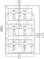
- Figure 1 illustrates schematically an example of a power supply system comprising a power converter 1, an electrical load 2 supplied by the power converter 1, an electrical supply network 3 connected to the power converter 2, and a control unit 4 connected to the power converter 2 with a wired connection 5.
- the electrical load 2 may be a three-phase motor 2a.
- the wired connection 5 may be an optical fibre.
- the power converter 1 comprises three identical switching arms 6a, 6b, 6c comprising each a first end 7 and a second end 8 connected to the electrical supply network 3 supplying the switching arms 6 and delivering for example a continuous voltage.
- Each switching arm 6a, 6b, 6c comprises a first switch 9 comprising a first end 10 connected to first end 7 of the switching arm 6a, 6b, 6c, a second end 11, and a control input 12 connected to a monitoring device 13 of the power converter.
- the monitoring device 13 may be disposed in the power converter 1.
- Each switching arms 6a, 6b, 6c further comprises a second switch 14 comprising a first end 15 connected to the second end 11 of the first switch 9, a second end 16 connected to the second end 8 of the switching arm 6a, 6b, 6c, and a control input 17 connected to the monitoring device 13.
- Each first and second switches 9, 14 comprise a transistor 18, a diode 19 and a gate driver 20.
- the diode 19 may be the internal diode of the transistor 19.
- the transistor 18 may be a MOSEFET "metal-oxide semiconductor field-effect transistor” transistor or an IGBT transistor "Insulated Gate Bipolar Transistor".
- the drain of the transistor 18 is connected to the first end 10, 15 and to the cathode of the diode 19 of the said switch 9, 14.
- the source of the transistor 18 is connected to the second end 11, 16 and to the anode of the diode 19 of the said switch 9, 14.
- the gate of the transistor 18 is connected to the gate driver 20.
- Each switching arm 6a, 6b, 6c comprises a power connection 20a, 20b, 20c between the first and second ends 15, 11 of the second and first switches 14, 9.
- Each power connection 20a, 20b, 20c is connected to a different phase of the load 2.
- the control unit 4 controls the gate drivers 20 so that the arms 6a, 6b, 6c supply the motor 2a with a balanced three-phase supply system generated from the network 3, the motor 2a generating a torque.
- control unit 4 controls the gate drivers 20 so that the motor 2a generates electric power from a torque applied on a rotor shaft of the motor 2a, the electric power being injected in the network 3 by the power converter 1.
- the power supply system further comprises a monitoring system for monitoring a control signal generated by the control unit 4 and received by the monitoring device 13 through the wired connection 5, the control signal controlling the switches 9, 14.
- the monitoring system comprises the control unit 4 and the monitoring device 13 connected with the control unit 4 through the wired connection 5.
- Figure 2 illustrates an example of the monitoring system.
- the control unit 4 comprises a clock 21 generating a clock signal Sclock at a predetermined frequency Fc, a control module 22, a merging circuit 23, a transmitter, and a processing unit 25.
- the control module 22 comprises an algorithm ALGO and generates a first variable signal S1 comprising instructions to control the switches 9, 14 of the power converter 1.
- the algorithm ALGO comprises for example a PWM control algorithm "Pulse Width Modulation".
- the merging circuit 23 comprises a XOR logical operator to merge the clock signal Sclock and the first variable signal S1, and delivers a first control signal Sc to the transmitter 24.
- the transmitter 24 delivers the first control signal Sc on the wired connection 5.
- the processing unit 25 implements the clock 21, the control module 22, the merging circuit 23 and the transmitter 24.
- the monitoring device 13 comprises a receiving circuit 26 for receiving the first control signal Sc from the wired connection 5 connected to a determining circuit 27 and a decoding circuit 28, a monitoring circuit 29 connected to the determining circuit 27 and the control unit 4 through a feed-back wired connection 30, and a control circuit 31 connected to the decoding circuit 28 and the gate drives of the first and second switches 9, 14.
- the determining circuit 27 determines if a change of state of the control signal Sc occurs during each period Tclock associated to the predetermined frequency Fclock.
- the monitoring circuit 29 sends a message to the control unit 4 through the feed-back wired connection 30 so that the processing unit 25 stops the transmission of the control signal Sc to the power converter 1.
- the power converter 1 stops to supply the electrical load according to the instructions of the control signal Sc.
- control signal Sc comprises the clock signal Sclock
- the state of the control signal Sc changes at least one time every period Tclock.
- the determining circuit 27 detects the change of the state of the control signal Sc.
- the monitoring circuit 29 concludes that the transmission of the control signal Sc from the control unit 4 to the monitoring device 13 is interrupted and warns the control unit 4.
- the decoding circuit 28 decodes the control signal Sc to extract the first variable signal S1 and sends the extracted first variable signal S1 to the control circuit 31 for controlling the gate drivers 20.
- the control circuit 31 conditions the signal S1 to control the gate drivers 20 and delivers a variable control signal S31 driving the gate drivers 20.
- Figure 3 illustrates schematically an example of the decoding circuit 28.
- the decoding circuit 28 comprises a NOT logical operator 32 receiving the control signal Sc.
- the decoding circuit 28 comprises a switch 33 comprising a first input 34 receiving the control signal Sc, a second input 35 connected to an output of the NOT logical operator 32, and a control input 36.
- the decoding circuit 28 further comprises a phase-locked loop 37 connected to an output of the switch 33.
- the decoding circuit 28 further comprises a first clock signal generator 38 and a second clock signal generator 39, both connected to an output of the phase-locked loop 37.
- the decoding circuit 28 further comprises a XOR logical operator 40 comprising a first input 41 receiving the control signal Sc and a second input 42 connected to an output of the first clock signal generator 38, and a gated D latch 50 comprising a data input 51 connected to an output of the XOR logical operator 40, a clock input 52 connected to an output of the second clock signal generator 39, and a reset input 53 connected to a second input 55 of the decoding circuit 28.
- a XOR logical operator 40 comprising a first input 41 receiving the control signal Sc and a second input 42 connected to an output of the first clock signal generator 38
- a gated D latch 50 comprising a data input 51 connected to an output of the XOR logical operator 40, a clock input 52 connected to an output of the second clock signal generator 39, and a reset input 53 connected to a second input 55 of the decoding circuit 28.
- the second input 55 is connected to a mass of the monitoring device 13.
- the gated D latch 50 comprises an output 54 connected to the control input 36 and to the control circuit 31.
- the phase-locked loop 37 tracks the frequency and the phase of a signal outputted by the switch 33.
- the switch 33 is controlled so that the phase of the signal at the input of the phase-locked loop 37 is not inverted to avoid that the phase-locked loop 37 is defaulting during an inversion of the phase of the inputted signal.
- the first input 34 is connected to the output of the switch 33, and when the output 54 of the gated D latch 50 delivers a high state, for example a "1" in Boolean algebra, the second input 35 is connected to the output of the switch 33.
- the first clock generator 38 delivers a first intermediate signal S38 of the clock signal Sclock, the frequency of the first intermediate signal S38 being equal to determined frequency by the phase-locked loop 37, and the phase of the first intermediate signal S38 being equal to the determined phase so that the first intermediate signal S38 is an estimation of the clock signal Sclock.
- the second clock generator 39 delivers a second intermediate signal S39, the frequency of second intermediate signal being equal to twice the determined frequency and the phase of the second intermediate S39 signal being shifted so that the raising edge of the second intermediate signal S39 is centred on the middle of the high state of the first intermediate signal S38.
- the XOR logical operator 40 delivers an intermediate control signal S40 indicative of the first variable signal S1.
- the accuracy of the signal S40 depends on the accuracy of the clock estimation signal S38 delivers by the first clock generator 38.
- the clock estimation signal S38 presents small shift phase compared to the clock signal Sclock generated by the clock 21 involving unexpected behaviour on the intermediate control signal S40 resulting from the XOR logical operator 40.
- the intermediate control signal S40 is sampled by the gated D latch 50 using the second intermediate signal S39.
- the output 54 of the gated D latch 50 delivers a signal S11 equal to the first variable signal S1 within a predetermined value chosen so that the converter 1 supplies the load 3 as expected.
- Figure 4 illustrates schematically an example of the determining circuit 27.
- the determining circuit 27 comprises a self-timer 60 receiving the first control signal Sc and outputting the first control signal Sc delayed from one period Tclock, an AND logical operator 61 comprising a first input receiving the first control signal Sc and a second input connected to the output of the self-timer 60.
- the determining circuit 27 further comprises a switch 62 comprising a first input 63 connected to a mass delivering a "0" in Boolean algebra, a second input 64 and a control input 65 connected to an output of the AND logical operator 61.
- An output of the switch 62 is connected to a first input of an adder 66.
- a memory 67 delivers the value of the period Tclock on a second input of the adder 66.
- An output of the adder 66 delivers the sum of the signals received on his first and second inputs to the second input 64 of the switch 62 and to an input of a comparator 68.
- the comparator 68 compares the received value to the value of the period Tclock.
- the output of the comparator 68 is connected to the feed-back wired connection 30.
- the determining circuit 27 further comprises a second output 69 connected to the output of the AND logical operator 61.
- the second output 69 is used when the monitoring system comprises two monitoring devices as described in the following.
- the AND logical operator 61 delivers a logical "1" so that the switch 62 connects the second input 64 with the output of the switch 62.
- the output of the adder 66 delivers at period Tn the sum of the output of the adder at period Tn-1 and the value of the period Tclock delivers by the memory 67.
- the comparator 68 delivers a logical "0" to the monitoring circuit 29 so that the monitoring circuit 29 does not send a message to stop the transmission of the first control signal Sc.
- the AND logical operator 61 delivers a logical "0" so that the switch 62 connects the first input 63 with the output of the switch 62.
- the output of the adder 66 delivers at period Tn the sum of the output of the adder at period Tn-1 and "0".
- the comparator 68 delivers a logical "1" to the monitoring circuit 29 so that the monitoring circuit 29 sends a message to stop the transmission of the first control signal Sc.
- FIG. 5 illustrates schematically another example of the monitoring system.
- the monitoring comprises the control unit 4, the monitoring device 13, a second monitoring device 70 different from the monitoring device 13 in that it does not comprise the monitoring circuit 29, and a selection circuit 71.
- the control unit 4 further comprises a second clock 210 generating a second clock signal Sclock2 at the predetermined frequency Fc, a second merging circuit 230, and a second transmitter 240.
- the second merging circuit 230 comprises a XOR logical operator to merge the second clock signal Sclock2 and the first variable signal S1, and delivers a second control signal Sc2 to the second transmitter 240.
- the second transmitter 240 delivers the second control signal Sc2 on a second wired connection 720, for example an optical fibre.
- the second control signal Sc2 is received by the receiving circuit 26 of the second monitoring device 70 through the second wired connection 720.
- the processing unit 25 further implements the second clock 210, the second merging circuit 230 and the second transmitter 240.
- the second monitoring device 70 delivers a variable control signal S32 to control the gate drivers 20.
- the signals S31, S32 delivered by the control circuits 31 of the monitoring devices 13, 70 are identical.
- the monitoring device 13 is connected to the control unit 4 through the wired connection 5 and the feed-back wired connection 30 as described above.
- the selection circuit 71 comprises eight inputs 72, 73, 74, 75, 76, 77, 78, 79 and one output 80.
- a first input 72 and a fifth input 76 are connected to the output of the control circuit 31 respectively of the monitoring device 13 and the second monitoring device 70.
- a second input 73 and a sixth input 77 are connected to the second output 55 of the decoding circuit 28 respectively of the monitoring device 13 and the second monitoring device 70.
- a third input 74 and a seventh input 78 are connected to the output of the determining circuit 27 respectively of the monitoring device 13 and the second monitoring device 70.
- a fourth input 75 and an eighth input 79 are connected to the second output 69 of the determining circuit 27 respectively of the monitoring device 13 and the second monitoring device 70.
- the output 80 is connected to the gate drivers 20.
- the selection circuit 71 determines which one of the monitoring devices 13 and the second monitoring device 70 is first ready for controlling the gates 20 of the power converter, and connects the control circuit 31 of the first ready monitoring device with the gates drivers 20.
- the selection circuit 71 connects the control circuit 31 of the functional monitoring device 13, 70 to the gate drivers 20 so that the load 2 is still supplied by the power converter 1, and the monitoring circuit 29 sends a message to the control unit 4 to stop the transmission of the control signal by the transmitter connected to the monitoring device detecting the fault.
- the power converter is still controlled by the other decoded variable signal S31, S32 as long as the other control signal S31, S32 is transmitted to the power controller.
- the monitoring devices 13, 70 and the selection circuit 71 provide a redundancy so that the power controller 1 is still control to supply the load 2 when one monitoring device 13, 70 detects a fault.
- Figure 6 illustrates schematically an example of the selection circuit 71.
- the selection circuit 71 comprises two identical monitoring units 81, 82 and a switching circuit 83.
- Each monitoring unit 81, 82 comprises a first input 84, a second input 85, a third input 86, a fourth input 87.
- a first monitoring unit 81 further comprises an output 881 and the second monitoring unit 82 further comprises an output 882.
- the first input 84 of the first monitoring unit 81 and the first input 84 of the second monitoring unit 82 are respectively connected to the first and the fifth inputs 72, 76 of the selection circuit 71.
- the second input 85 of the first monitoring unit 81 and the second input 85 of the second monitoring unit 82 are respectively connected to the second and sixth inputs 73, 77 of the selection circuit 71.
- the third input 86 of the first monitoring unit 81 and the third input 86 of the second monitoring unit 82 are respectively connected to the fourth input 75 and an eighth input 79 of the selection circuit 71.
- the fourth input 87 of a first monitoring unit 81 and the fourth input 87 of the second monitoring unit 82 are respectively connected to the third input 74 and a seventh input 78 of the selection circuit 71.
- the switching circuit 83 comprises six inputs 88, 89, 90, 91, 92, 93 and one output 94.
- a first input 88 and a fourth input 91 are respectively connected to the first and fifth inputs 72, 76 of the selection circuit 71.
- a second input 89 and a fifth input 92 are respectively connected to the outputs 881, 882 of the monitoring unit 81, 82.
- a third input 90 and a sixth input 93 are respectively connected to the third input 74 and a seventh input 78 of the selection circuit 71.
- the output 94 of the switching circuit 83 is connected to the output 80 of the selection circuit 71.
- figure 7 illustrates schematically an example of the monitoring unit 81.
- the monitoring unit 81 comprises a switch 95 comprising a first input 96 connected to a mass delivering a "0" in Boolean algebra, a second input 97, and a control input 98 connected to the third input 86 of the first monitoring unit 81.
- the second input 97 is connected with the output 99.
- the third input 86 delivers a "0" in Boolean algebra
- the first input 96 is connected with the output 99.
- An output of the switch 99 is connected to a first input of an adder 100.
- a memory 101 delivers a value of an initialisation value Tinit on a second input of the adder 100.
- the initialisation value Tinit is equal or greater than the starting time of the control unit 4 and is for example equal to 1 second.
- An output of the adder 100 delivers the sum of the signals received on his first and second inputs to the second input 97 of the switch 95 and to an input of a comparator 102.
- the comparator 102 compares the received value to the value of the initialisation value Tinit.
- the comparator 102 If the received value is greater than the initialisation value Tinit, the comparator 102 generates an "1" in Boolean algebra on a set input 104 of a latch 103, and "0" otherwise.
- the RS latch 103 is a set-reset latch.
- An output 105 of the RS latch 103 is connected to the second input 85 of the first monitoring unit 81 and a first input 106 of a AND logical operator 107.
- the reset input 108 of the RS latch 103 is connected to a reset input 109 of a second RS latch 108 and the output 881.
- a set input 110 of the second RS latch 108 is connected to an output 111 of the AND logical operator 107.
- An output 112 of the second RS latch 108 is connected to a control input 113 of a second switch 114.
- the second switch 114 further comprises a first input 115 connected to a mass delivering a "0" in Boolean algebra, a second input 116 and an output 117.
- the second input 116 is connected with the output 117.
- the first input 115 is connected with the output 117.
- the output 117 of the second switch 114 is connected to a first input of a second adder 118.
- the memory 101 delivers a value of an initialisation delay Tinit on a second input of the second adder 118.
- An output of the second adder 118 delivers the sum of the signals received on his first and second inputs to an input of a second comparator 119.
- the comparator 119 compares the received value to the value of the initialisation value Tinit.
- the second comparator 119 If the received value is smaller than the initialisation value Tinit, the second comparator 119 generates an "1" in Boolean algebra on the output 881 and "0" otherwise.
- a first input of a OR logical operator 120 is connected to the first input 72, and a second input of the OR logical operator 120 is connected to the third input 74.
- An output of the OR logical operator 120 is connected to the input of a NOT logical operator 121.
- An output 112 of the NOT logical operator 121 is connected to a control input 122 of a third switch 123.
- the third switch 123 further comprises a first input 124 connected to a mass delivering a "0" in Boolean algebra, and comprises a second input 125 and an output 126.
- the second input 125 is connected with the output 126.
- the first input 124 is connected with the output 126.
- the output 126 of the third switch 123 is connected to a first input of a third adder 127.
- the memory 101 delivers a value of an initialisation delay Tinit on a second input of the second adder 127.
- An output of the third adder 127 delivers the sum of the signals received on his first and second inputs to an input of a third comparator 128.
- the third comparator 128 compares the received value to the value of the initialisation value Tinit.
- the third comparator 128 If the received value is greater than the initialisation value Tinit, the third comparator 128 generates an "1" in Boolean algebra on a second input 129 of the AND logical operator 107 and "0" otherwise.
- the first and second monitoring units 81, 82 determine respectively when the first and the second monitoring devices 70, 13 are ready to deliver the signals S31, S32 to drive the gate drivers 20.
- the transmitters are ready if the monitoring unit 81, 82 received the clock signal Sclock, Sclock2 during at least the duration Tinit.
- Figure 8 illustrates schematically an example of the switching circuit 83.
- the switching circuit 83 comprises a first latch 130 and a second latch 136, the first and second latches 130, 136 being set-reset latches.
- the first latch 130 comprises a set input 131 connected to the second input 89 of the switching circuit 83, a reset input 132 connected to the third input 90 of the switching circuit 83, and an output 133 connected to an input of a logical NOT operator 134 and to a first input of a logical XOR operator 135.
- the second latch 136 comprises a set input 137 connected to the fifth input 92 of the switching circuit 83, a reset input 138 connected to the sixth input 93 of the switching circuit 83, and an output 139 connected to a first input of a logical AND operator 140 and to a second input of the logical XOR operator 135.
- An output of the logical AND operator 140 is connected to a data input 1400 of a gated D latch 141.
- the gated D latch 141 comprises a clock input 142 connected to an output of logical XOR operator 135, and an output 143 connected to a control input 144 of a switch 145.
- the switch 145 further comprises a first input 146 connected to the first input 88, a second input 147 connected to the fourth input 91, and an output 148 connected to the output 94.
- the monitoring unit 81 detects that the monitoring device 13 is first ready to drive the gate drivers 20, the first input 146 of the switch 145 is connected to the output 148.
- the second monitoring unit 82 detects that the second monitoring device 70 is first ready to drive the gate drivers 20, the second input 147 of the switch 145 is connected to the output 148.
Abstract
A monitoring device (13) for monitoring a control signal (Sc) received by a power converter (1), the control signal controlling switches (9, 14) to supply an electrical load (2) is proposed.The monitoring device comprising:- a receiving circuit (26) for receiving the control signal (Sc) comprising a merging of a first variable signal (S1) and a clock signal (Sclock) having a predetermined frequency greater than the first variable signal,- a determining circuit (27) for determining if a change of state of the control signal (Sc) occurs during each period associated to the predetermined frequency, and- a monitoring circuit (29) for stopping the transmission of the control signal to the power converter so that the power converter stops to supply the electrical load according to the instructions of the first variable signal if a change of state of the control signal does not occur during one period.
Description
- The present invention concerns power converts and relates more particularly to the monitoring of signals received by power converters to control the switches of the power converters.
- The present invention also relates to a method and a system for monitoring a control signal received by a power converter.
- A power converter is generally controlled by a controlling unit comprising an interface board connected by a wired connection to an interface board of the power converter.
- The wired connection may comprise fibres, the wired connection being an optical connection.
- The controlling unit generates control signals to control switches of the power controller so that the controller delivers for example a sinusoidal power signal from a continuous power source to supply an electrical load.
- The switches may comprise power transistors.
- The interface board of the power converter is connected to gate drivers of the power converter controlling the power transistors.
- The control signals may be PWM control signals "Pulse Width Modulation" varying between a high logical state and a low logical state.
- The low logical state may be a null voltage and is generally indicative of an off state of the power transistors.
- When the interface board of the power converter receives a low logical state, the power converter is not able to determine if the null logical state is generated by the controlling unit or is the result of for example a breakdown of the wired connection, a failure of an interface board or a bad connection of the wired connection and an interface board.
- A misinterpretation of the low logical state by the gate drives may generate an overcurrent in the power controller causing a failure of the power converter.
- It is therefore proposed to remedy the disadvantage related to the transmission of control signals, and more particularly to determine if the low logical state is generated to control the power controller or results from a failure.
- In view of the foregoing the invention proposes a method for monitoring a control signal received by a power converter, the control signal controlling switches of the power converter to supply an electrical load.
- The method comprising:
- receiving by the power converter a control signal comprising a merging of a first variable signal and a clock signal having a predetermined frequency greater than the first variable signal, the first variable signal comprising instructions to control the switches,
- determining if a change of state of the control signal occurs during each period associated to the predetermined frequency, and
- if a change of state of the control signal does not occur during one period, stopping the transmission of the control signal to the power converter so that the power converter stops to supply the electrical load according to the instructions of the first variable signal.
- Preferably, merging the first variable signal and the clock signal comprises combining the first variable signal and the clock signal by XOR logical operator to obtain the control signal.
- Advantageously, when a change of state of the control signal occurs during each period, the method further comprises:
- decoding the control signal by a decoding circuit of the power control to extract the first variable signal,
- controlling the power converter according to the decoded first variable signal.
- Preferably, decoding the control signal comprises:
- determining the frequency and the phase of the clock signal from the control signal,
- providing two intermediate signals from the determined frequency and phase,
the frequency of a first intermediate signal being equal to the determined frequency and the phase of the first intermediate signal being equal to the determined phase so that the first intermediate signal is an estimation of the clock signal, and the frequency of second intermediate signal being equal to twice the determined frequency and the phase of the second intermediate signal being shifted so that the raising edge of the second intermediate signal is centred on the middle of the high state of the first intermediate signal - combining the control signal and first intermediate signal by XOR logical operator to obtain an intermediate control signal, and
- sampling the intermediate control signal with the raising edge of the second intermediate signal to generate a first variable control signal within a predetermine value, the first variable control signal being configured to control the switches.
- Advantageously, the method further comprises:
- determining if a change of state of a second control signal occurs during each period associated to the predetermined frequency, the second control signal comprising the variable signal comprising instructions to control the switches merged with a second clock signal having the predetermined frequency,
- if a change of state of a second control signal occurs during each period associated to the predetermined frequency, decoding the second control signal to extract a second variable control signal, and
- if the transmission of the control signal to the power converter is stopped, controlling the power converter according to the second variable signal.
- Preferably, if the transmission of the control signal to the power converter is transmitted again, the power converter is still controlled by the second variable control signal as long as the second control signal is transmitted to the power controller.
- Another object of the invention relates to a monitoring device for monitoring a control signal received by a power converter, the control signal controlling switches of the power converter to supply an electrical load.
- The monitoring device comprises:
- a receiving circuit for receiving the control signal comprising a merging of a first variable signal and a clock signal having a predetermined frequency greater than the first variable signal, the first variable signal comprising instructions to control the switches,
- a determining circuit for determining if a change of state of the control signal occurs during each period associated to the predetermined frequency, and
- a monitoring circuit for stopping the transmission of the control signal to the power converter so that the power converter stops to supply the electrical load according to the instructions of the first variable signal if a change of state of the control signal does not occur during one period.
- Advantageously, the monitoring device further comprises:
- a decoding circuit for decoding the control signal to extract a first variable control signal, and
- a control circuit for controlling the power converter according to the first variable control signal,
- determine the frequency and the phase of the clock signal from the control signal,
- provide two intermediate signals from the determined frequency and phase,
the frequency of a first intermediate signal being equal to the determined frequency and the phase of the first intermediate signal being equal to the determined phase so that the first intermediate signal is an estimation of the clock signal, and the frequency of second intermediate signal being equal to twice the determined frequency and the phase of the second intermediate signal being shifted so that the raising edge of the second intermediate signal is centred on the middle of the high state of the first intermediate signal, - combine the control signal and first intermediate signal by XOR logical operator to obtain an intermediate control signal, and
- sample the intermediate control signal with the raising edge of the second intermediate signal to generate the first variable control signal within a predetermined value when a change of state of the control signal occurs at each period.
- Another object of the invention relates to a monitoring system for monitoring a control signal received by a power converter comprising:
- at least one monitoring device as defined above, and
- a control unit connected to the receiving circuit of the monitoring device with a first wired connection,
the control unit comprising a merging circuit to merge the first variable signal and the clock signal by a XOR logical operator to obtain the control signal and a transmitter to transmit the control signal to the monitoring device through the first wired connection. - Advantageously, the monitoring system further comprises a second monitoring device as defined above, a second wired connection connecting the receiving circuit of the second monitoring device to the control unit, and a selection circuit, the control unit further comprising:
- a second merging circuit to merge the first variable signal with a second clock signal having the predetermined frequency to obtain a second control variable signal,
- a second transmitter transmitting the second control signal to the second monitoring device through the second wired connection,
the selection circuit being configured to transmit the extracted second variable control signal to control the switches of the power converter to supply the electrical load according to the instructions of the extracted second variable signal if a change of state of the second control signal occurs during each period associated to the predetermined frequency and if the transmission of the control signal to the power converter is stopped. - Preferably, the selection circuit is further configured to still transmit the second variable control signal if the transmission of the control signal to the power converter is transmitted again as long as the second control signal is transmitted to the power controller.
- Another object of the invention relates to a power supply system comprising a converter including gate drivers driving the switches of the power converter, and a monitoring system as defined above, each monitoring device being coupled to the gate drivers.
- Other characteristics and advantages of the invention will emerge on reading the following description of embodiments of the invention, provided solely by way of non-limiting examples and with reference to the drawings in which:
-
Figure 1 illustrates an example of a power supply system according to the invention, -
Figure 2 illustrates an example of the monitoring system according to the invention, -
Figure 3 illustrates an example of the decoding circuit according to the invention, -
Figure 4 illustrates an example of the determining circuit according to the invention, -
Figure 5 illustrates another example of the monitoring system according to the invention, -
Figure 6 illustrates an example of the selection circuit according to the invention, -
Figure 7 illustrates an example of a monitoring unit according to the invention, and -
Figure 8 illustrates an example of switching circuit according to the invention, -
Figure 1 illustrates schematically an example of a power supply system comprising apower converter 1, anelectrical load 2 supplied by thepower converter 1, anelectrical supply network 3 connected to thepower converter 2, and acontrol unit 4 connected to thepower converter 2 with awired connection 5. - The
electrical load 2 may be a three-phase motor 2a. - The
wired connection 5 may be an optical fibre. - The
power converter 1 comprises three identical switchingarms first end 7 and asecond end 8 connected to theelectrical supply network 3 supplying the switching arms 6 and delivering for example a continuous voltage. - Each switching
arm first switch 9 comprising afirst end 10 connected tofirst end 7 of theswitching arm second end 11, and acontrol input 12 connected to amonitoring device 13 of the power converter. - The
monitoring device 13 may be disposed in thepower converter 1. - Each switching
arms second switch 14 comprising afirst end 15 connected to thesecond end 11 of thefirst switch 9, asecond end 16 connected to thesecond end 8 of theswitching arm control input 17 connected to themonitoring device 13. - Each first and
second switches transistor 18, adiode 19 and agate driver 20. - The
diode 19 may be the internal diode of thetransistor 19. - The
transistor 18 may be a MOSEFET "metal-oxide semiconductor field-effect transistor" transistor or an IGBT transistor "Insulated Gate Bipolar Transistor". - The drain of the
transistor 18 is connected to thefirst end diode 19 of the saidswitch - The source of the
transistor 18 is connected to thesecond end diode 19 of the saidswitch - The gate of the
transistor 18 is connected to thegate driver 20. - Each switching
arm power connexion first switches - Each
power connexion load 2. - The
control unit 4 controls thegate drivers 20 so that thearms motor 2a with a balanced three-phase supply system generated from thenetwork 3, themotor 2a generating a torque. - In another embodiment, the
control unit 4 controls thegate drivers 20 so that themotor 2a generates electric power from a torque applied on a rotor shaft of themotor 2a, the electric power being injected in thenetwork 3 by thepower converter 1. - The power supply system further comprises a monitoring system for monitoring a control signal generated by the
control unit 4 and received by themonitoring device 13 through thewired connection 5, the control signal controlling theswitches - The monitoring system comprises the
control unit 4 and themonitoring device 13 connected with thecontrol unit 4 through thewired connection 5. -
Figure 2 illustrates an example of the monitoring system. - The
control unit 4 comprises aclock 21 generating a clock signal Sclock at a predetermined frequency Fc, acontrol module 22, a mergingcircuit 23, a transmitter, and aprocessing unit 25. - The
control module 22 comprises an algorithm ALGO and generates a first variable signal S1 comprising instructions to control theswitches power converter 1. - The algorithm ALGO comprises for example a PWM control algorithm "Pulse Width Modulation".
- The merging
circuit 23 comprises a XOR logical operator to merge the clock signal Sclock and the first variable signal S1, and delivers a first control signal Sc to thetransmitter 24. - The
transmitter 24 delivers the first control signal Sc on thewired connection 5. - The
processing unit 25 implements theclock 21, thecontrol module 22, the mergingcircuit 23 and thetransmitter 24. - The
monitoring device 13 comprises a receivingcircuit 26 for receiving the first control signal Sc from thewired connection 5 connected to a determiningcircuit 27 and adecoding circuit 28, amonitoring circuit 29 connected to the determiningcircuit 27 and thecontrol unit 4 through a feed-backwired connection 30, and acontrol circuit 31 connected to thedecoding circuit 28 and the gate drives of the first andsecond switches - The determining
circuit 27 determines if a change of state of the control signal Sc occurs during each period Tclock associated to the predetermined frequency Fclock. The period Tclock is equal to:
- If during a period Tclock the determining
circuit 27 determines that no change of state of the control signal Sc occurs during at least one period Tclock, themonitoring circuit 29 sends a message to thecontrol unit 4 through the feed-backwired connection 30 so that theprocessing unit 25 stops the transmission of the control signal Sc to thepower converter 1. - The
power converter 1 stops to supply the electrical load according to the instructions of the control signal Sc. - As the control signal Sc comprises the clock signal Sclock, the state of the control signal Sc changes at least one time every period Tclock.
- As long as the
monitoring device 13 receives the control signal Sc, the determiningcircuit 27 detects the change of the state of the control signal Sc. - When the determining
circuit 27 does not detect the change of the state of the control signal Sc, themonitoring circuit 29 concludes that the transmission of the control signal Sc from thecontrol unit 4 to themonitoring device 13 is interrupted and warns thecontrol unit 4. - As long as the determining
circuit 27 detects a change of the state of the control signal Sc during the period Tclock, thedecoding circuit 28 decodes the control signal Sc to extract the first variable signal S1 and sends the extracted first variable signal S1 to thecontrol circuit 31 for controlling thegate drivers 20. - The
control circuit 31 conditions the signal S1 to control thegate drivers 20 and delivers a variable control signal S31 driving thegate drivers 20. -
Figure 3 illustrates schematically an example of thedecoding circuit 28. - The
decoding circuit 28 comprises a NOTlogical operator 32 receiving the control signal Sc. - The
decoding circuit 28 comprises aswitch 33 comprising afirst input 34 receiving the control signal Sc, asecond input 35 connected to an output of the NOTlogical operator 32, and acontrol input 36. - The
decoding circuit 28 further comprises a phase-lockedloop 37 connected to an output of theswitch 33. - The
decoding circuit 28 further comprises a firstclock signal generator 38 and a secondclock signal generator 39, both connected to an output of the phase-lockedloop 37. - The
decoding circuit 28 further comprises a XORlogical operator 40 comprising afirst input 41 receiving the control signal Sc and asecond input 42 connected to an output of the firstclock signal generator 38, and agated D latch 50 comprising adata input 51 connected to an output of the XORlogical operator 40, aclock input 52 connected to an output of the secondclock signal generator 39, and a reset input 53 connected to asecond input 55 of thedecoding circuit 28. - The
second input 55 is connected to a mass of themonitoring device 13. - The
gated D latch 50 comprises anoutput 54 connected to thecontrol input 36 and to thecontrol circuit 31. - The phase-locked
loop 37 tracks the frequency and the phase of a signal outputted by theswitch 33. - The
switch 33 is controlled so that the phase of the signal at the input of the phase-lockedloop 37 is not inverted to avoid that the phase-lockedloop 37 is defaulting during an inversion of the phase of the inputted signal. - When the
output 54 of thegated D latch 50 delivers a low state, for example a "0" in Boolean algebra, thefirst input 34 is connected to the output of theswitch 33, and when theoutput 54 of thegated D latch 50 delivers a high state, for example a "1" in Boolean algebra, thesecond input 35 is connected to the output of theswitch 33. - The
first clock generator 38 delivers a first intermediate signal S38 of the clock signal Sclock, the frequency of the first intermediate signal S38 being equal to determined frequency by the phase-lockedloop 37, and the phase of the first intermediate signal S38 being equal to the determined phase so that the first intermediate signal S38 is an estimation of the clock signal Sclock. - The
second clock generator 39 delivers a second intermediate signal S39, the frequency of second intermediate signal being equal to twice the determined frequency and the phase of the second intermediate S39 signal being shifted so that the raising edge of the second intermediate signal S39 is centred on the middle of the high state of the first intermediate signal S38. - The XOR
logical operator 40 delivers an intermediate control signal S40 indicative of the first variable signal S1. - The accuracy of the signal S40 depends on the accuracy of the clock estimation signal S38 delivers by the
first clock generator 38. - The clock estimation signal S38 presents small shift phase compared to the clock signal Sclock generated by the
clock 21 involving unexpected behaviour on the intermediate control signal S40 resulting from the XORlogical operator 40. - To enhance the accuracy of the estimated first variable signal S1 by the
monitoring device 13, the intermediate control signal S40 is sampled by thegated D latch 50 using the second intermediate signal S39. - The
output 54 of thegated D latch 50 delivers a signal S11 equal to the first variable signal S1 within a predetermined value chosen so that theconverter 1 supplies theload 3 as expected. -
Figure 4 illustrates schematically an example of the determiningcircuit 27. - The determining
circuit 27 comprises a self-timer 60 receiving the first control signal Sc and outputting the first control signal Sc delayed from one period Tclock, an ANDlogical operator 61 comprising a first input receiving the first control signal Sc and a second input connected to the output of the self-timer 60. - The determining
circuit 27 further comprises aswitch 62 comprising afirst input 63 connected to a mass delivering a "0" in Boolean algebra, asecond input 64 and acontrol input 65 connected to an output of the ANDlogical operator 61. - An output of the
switch 62 is connected to a first input of anadder 66. - A
memory 67 delivers the value of the period Tclock on a second input of theadder 66. - An output of the
adder 66 delivers the sum of the signals received on his first and second inputs to thesecond input 64 of theswitch 62 and to an input of acomparator 68. - The
comparator 68 compares the received value to the value of the period Tclock. - The output of the
comparator 68 is connected to the feed-backwired connection 30. - The determining
circuit 27 further comprises asecond output 69 connected to the output of the ANDlogical operator 61. - The
second output 69 is used when the monitoring system comprises two monitoring devices as described in the following. - It is assumed that at a period Tn-1, n being an integer greater than one, a change of state of the control signal Sc is detected, Tn being the current period so that the output of the
adder 66 is greater than or equal to the period Tclock. - As long as the state of the control signal Sc changes during each period Tclock, the AND
logical operator 61 delivers a logical "1" so that theswitch 62 connects thesecond input 64 with the output of theswitch 62. - The output of the
adder 66 delivers at period Tn the sum of the output of the adder at period Tn-1 and the value of the period Tclock delivers by thememory 67. - As the value of the value received by the
comparator 68 is greater than the period Tclock, thecomparator 68 delivers a logical "0" to themonitoring circuit 29 so that themonitoring circuit 29 does not send a message to stop the transmission of the first control signal Sc. - As soon as the state of the control signal Sc does not change during one period Tclock, the AND
logical operator 61 delivers a logical "0" so that theswitch 62 connects thefirst input 63 with the output of theswitch 62. - The output of the
adder 66 delivers at period Tn the sum of the output of the adder at period Tn-1 and "0". - As the value of the value received by the
comparator 68 is equal to the period Tclock, thecomparator 68 delivers a logical "1" to themonitoring circuit 29 so that themonitoring circuit 29 sends a message to stop the transmission of the first control signal Sc. -
Figure 5 illustrates schematically another example of the monitoring system. - The monitoring comprises the
control unit 4, themonitoring device 13, asecond monitoring device 70 different from themonitoring device 13 in that it does not comprise themonitoring circuit 29, and aselection circuit 71. - The
control unit 4 further comprises asecond clock 210 generating a second clock signal Sclock2 at the predetermined frequency Fc, asecond merging circuit 230, and asecond transmitter 240. - The
second merging circuit 230 comprises a XOR logical operator to merge the second clock signal Sclock2 and the first variable signal S1, and delivers a second control signal Sc2 to thesecond transmitter 240. - The
second transmitter 240 delivers the second control signal Sc2 on a secondwired connection 720, for example an optical fibre. - The second control signal Sc2 is received by the receiving
circuit 26 of thesecond monitoring device 70 through the secondwired connection 720. - The
processing unit 25 further implements thesecond clock 210, thesecond merging circuit 230 and thesecond transmitter 240. - The
second monitoring device 70 delivers a variable control signal S32 to control thegate drivers 20. - Generally, the signals S31, S32 delivered by the
control circuits 31 of themonitoring devices - The
monitoring device 13 is connected to thecontrol unit 4 through thewired connection 5 and the feed-backwired connection 30 as described above. - The
selection circuit 71 comprises eightinputs output 80. - A
first input 72 and afifth input 76 are connected to the output of thecontrol circuit 31 respectively of themonitoring device 13 and thesecond monitoring device 70. - A
second input 73 and asixth input 77 are connected to thesecond output 55 of thedecoding circuit 28 respectively of themonitoring device 13 and thesecond monitoring device 70. - A
third input 74 and aseventh input 78 are connected to the output of the determiningcircuit 27 respectively of themonitoring device 13 and thesecond monitoring device 70. - A
fourth input 75 and aneighth input 79 are connected to thesecond output 69 of the determiningcircuit 27 respectively of themonitoring device 13 and thesecond monitoring device 70. - The
output 80 is connected to thegate drivers 20. - At the start-up of the power supply system, the
selection circuit 71 determines which one of themonitoring devices 13 and thesecond monitoring device 70 is first ready for controlling thegates 20 of the power converter, and connects thecontrol circuit 31 of the first ready monitoring device with thegates drivers 20. - Further, when the present monitoring device controlling the
gates 20 detects a fault and the other monitoring device is ready to deliver the signal S31, S32, theselection circuit 71 connects thecontrol circuit 31 of thefunctional monitoring device gate drivers 20 so that theload 2 is still supplied by thepower converter 1, and themonitoring circuit 29 sends a message to thecontrol unit 4 to stop the transmission of the control signal by the transmitter connected to the monitoring device detecting the fault. - If the transmission of the control signal to the power converter is transmitted again by the monitoring device detecting the fault after repairing, the power converter is still controlled by the other decoded variable signal S31, S32 as long as the other control signal S31, S32 is transmitted to the power controller.
- The
monitoring devices selection circuit 71 provide a redundancy so that thepower controller 1 is still control to supply theload 2 when onemonitoring device -
Figure 6 illustrates schematically an example of theselection circuit 71. - The
selection circuit 71 comprises twoidentical monitoring units switching circuit 83. - Each
monitoring unit first input 84, asecond input 85, athird input 86, afourth input 87. - A
first monitoring unit 81 further comprises anoutput 881 and thesecond monitoring unit 82 further comprises anoutput 882. - The
first input 84 of thefirst monitoring unit 81 and thefirst input 84 of thesecond monitoring unit 82 are respectively connected to the first and thefifth inputs selection circuit 71. - The
second input 85 of thefirst monitoring unit 81 and thesecond input 85 of thesecond monitoring unit 82 are respectively connected to the second andsixth inputs selection circuit 71. - The
third input 86 of thefirst monitoring unit 81 and thethird input 86 of thesecond monitoring unit 82 are respectively connected to thefourth input 75 and aneighth input 79 of theselection circuit 71. - The
fourth input 87 of afirst monitoring unit 81 and thefourth input 87 of thesecond monitoring unit 82 are respectively connected to thethird input 74 and aseventh input 78 of theselection circuit 71. - The switching
circuit 83 comprises sixinputs output 94. - A
first input 88 and afourth input 91 are respectively connected to the first andfifth inputs selection circuit 71. - A
second input 89 and afifth input 92 are respectively connected to theoutputs monitoring unit - A
third input 90 and asixth input 93 are respectively connected to thethird input 74 and aseventh input 78 of theselection circuit 71. - The
output 94 of the switchingcircuit 83 is connected to theoutput 80 of theselection circuit 71. - As the
monitoring units figure 7 illustrates schematically an example of themonitoring unit 81. - The
monitoring unit 81 comprises aswitch 95 comprising afirst input 96 connected to a mass delivering a "0" in Boolean algebra, asecond input 97, and acontrol input 98 connected to thethird input 86 of thefirst monitoring unit 81. - When the
third input 86 delivers a "1" in Boolean algebra, thesecond input 97 is connected with theoutput 99. - When the
third input 86 delivers a "0" in Boolean algebra, thefirst input 96 is connected with theoutput 99. - An output of the
switch 99 is connected to a first input of anadder 100. - A
memory 101 delivers a value of an initialisation value Tinit on a second input of theadder 100. - The initialisation value Tinit is equal or greater than the starting time of the
control unit 4 and is for example equal to 1 second. - An output of the
adder 100 delivers the sum of the signals received on his first and second inputs to thesecond input 97 of theswitch 95 and to an input of acomparator 102. - The
comparator 102 compares the received value to the value of the initialisation value Tinit. - If the received value is greater than the initialisation value Tinit, the
comparator 102 generates an "1" in Boolean algebra on aset input 104 of alatch 103, and "0" otherwise. - The
RS latch 103 is a set-reset latch. - An
output 105 of theRS latch 103 is connected to thesecond input 85 of thefirst monitoring unit 81 and afirst input 106 of a ANDlogical operator 107. - The
reset input 108 of theRS latch 103 is connected to areset input 109 of asecond RS latch 108 and theoutput 881. - A
set input 110 of thesecond RS latch 108 is connected to anoutput 111 of the ANDlogical operator 107. - An
output 112 of thesecond RS latch 108 is connected to acontrol input 113 of asecond switch 114. - The
second switch 114 further comprises afirst input 115 connected to a mass delivering a "0" in Boolean algebra, asecond input 116 and anoutput 117. - When the
output 112 of thesecond RS latch 108 delivers a "1" in Boolean algebra, thesecond input 116 is connected with theoutput 117. - When the
output 112 of thesecond RS latch 108 delivers a "0" in Boolean algebra, thefirst input 115 is connected with theoutput 117. - The
output 117 of thesecond switch 114 is connected to a first input of asecond adder 118. - The
memory 101 delivers a value of an initialisation delay Tinit on a second input of thesecond adder 118. - An output of the
second adder 118 delivers the sum of the signals received on his first and second inputs to an input of asecond comparator 119. - The
comparator 119 compares the received value to the value of the initialisation value Tinit. - If the received value is smaller than the initialisation value Tinit, the
second comparator 119 generates an "1" in Boolean algebra on theoutput 881 and "0" otherwise. - A first input of a OR
logical operator 120 is connected to thefirst input 72, and a second input of the ORlogical operator 120 is connected to thethird input 74. - An output of the OR
logical operator 120 is connected to the input of a NOTlogical operator 121. - An
output 112 of the NOTlogical operator 121 is connected to acontrol input 122 of athird switch 123. - The
third switch 123 further comprises afirst input 124 connected to a mass delivering a "0" in Boolean algebra, and comprises asecond input 125 and anoutput 126. - When the output of the NOT
logical operator 121 delivers a "1" in Boolean algebra, thesecond input 125 is connected with theoutput 126. - When the output of the NOT
logical operator 121 delivers a "0" in Boolean algebra, thefirst input 124 is connected with theoutput 126. - The
output 126 of thethird switch 123 is connected to a first input of athird adder 127. - The
memory 101 delivers a value of an initialisation delay Tinit on a second input of thesecond adder 127. - An output of the
third adder 127 delivers the sum of the signals received on his first and second inputs to an input of athird comparator 128. - The
third comparator 128 compares the received value to the value of the initialisation value Tinit. - If the received value is greater than the initialisation value Tinit, the
third comparator 128 generates an "1" in Boolean algebra on asecond input 129 of the ANDlogical operator 107 and "0" otherwise. - The first and
second monitoring units second monitoring devices gate drivers 20. - The sequence to detect if the
transmitters - Only the clock signal Sclock, Sclock2 is received by the
monitoring device - Then a reset of the outputs of the
control unit 4 is set during the duration Tinit. - It is assumed that the transmitters are ready if the
monitoring unit -
Figure 8 illustrates schematically an example of the switchingcircuit 83. - The switching
circuit 83 comprises afirst latch 130 and asecond latch 136, the first andsecond latches - The
first latch 130 comprises a setinput 131 connected to thesecond input 89 of the switchingcircuit 83, areset input 132 connected to thethird input 90 of the switchingcircuit 83, and anoutput 133 connected to an input of alogical NOT operator 134 and to a first input of alogical XOR operator 135. - The
second latch 136 comprises a setinput 137 connected to thefifth input 92 of the switchingcircuit 83, areset input 138 connected to thesixth input 93 of the switchingcircuit 83, and anoutput 139 connected to a first input of a logical ANDoperator 140 and to a second input of thelogical XOR operator 135. - An output of the logical AND
operator 140 is connected to adata input 1400 of agated D latch 141. - The
gated D latch 141 comprises aclock input 142 connected to an output oflogical XOR operator 135, and anoutput 143 connected to acontrol input 144 of aswitch 145. - The
switch 145 further comprises afirst input 146 connected to thefirst input 88, asecond input 147 connected to thefourth input 91, and anoutput 148 connected to theoutput 94. - At the starting of the power supply system, if the
monitoring unit 81 detects that themonitoring device 13 is first ready to drive thegate drivers 20, thefirst input 146 of theswitch 145 is connected to theoutput 148. - If the
second monitoring unit 82 detects that thesecond monitoring device 70 is first ready to drive thegate drivers 20, thesecond input 147 of theswitch 145 is connected to theoutput 148.
Claims (12)
- Method for monitoring a control signal (Sc) received by a power converter (1), the control signal controlling switches (9, 14) of the power converter to supply an electrical load (2), characterized in that the method comprises:- receiving by the power converter the control signal comprising a merging of a first variable signal (S1) and a clock signal (Sclock) having a predetermined frequency greater than the first variable signal, the first variable signal comprising instructions to control the switches,- determining if a change of state of the control signal occurs during each period associated to the predetermined frequency, and- if a change of state of the control signal does not occur during one period, stopping the transmission of the control signal to the power converter so that the power converter stops to supply the electrical load according to the instructions of the first variable signal.
- Method according to claim 1, wherein merging the first variable signal (S1) and the clock signal (Sclock) comprises combining the first variable signal and the clock signal by XOR logical operator (23) to obtain the control signal (Sc).
- Method according to claims 1 or 2, further comprising when a change of state of the control signal occurs during each period:- decoding the control signal (Sc) by a decoding circuit (28) of the power control (1) to extract the first variable signal (S1),- controlling the power converter according to the decoded first variable signal.
- Method according to claim 3, wherein decoding the control signal comprises:- determining the frequency and the phase of the clock signal (Sclock) from the control signal (Sc),- providing two intermediate signals (S38, S39) from the determined frequency and phase,the frequency of a first intermediate signal (S38) being equal to the determined frequency and the phase of the first intermediate signal being equal to the determined phase so that the first intermediate signal is an estimation of the clock signal (Sclock), and the frequency of second intermediate (S39) signal being equal to twice the determined frequency and the phase of the second intermediate signal being shifted so that the raising edge of the second intermediate signal is centred on the middle of the high state of the first intermediate signal- combining the control signal (Sc) and first intermediate signal (S38) by XOR logical operator (40) to obtain an intermediate control signal (S40), and- sampling the intermediate control signal with the raising edge of the second intermediate signal to generate a first variable control signal (S31) b within a predetermine value, the first variable control signal being configured to control the switches (9, 14).
- Method according to any one of claims 1 to 4, further comprising:- determining if a change of state of a second control signal (Sc2) occurs during each period associated to the predetermined frequency, the second control signal comprising the variable signal (S1) comprising instructions to control the switches merged with a second clock signal (Sclock2) having the predetermined frequency,- if a change of state of a second control signal occurs during each period associated to the predetermined frequency, decoding the second control signal (Sc2) to extract a second variable control signal (S32), and- if the transmission of the control signal to the power converter (1) is stopped, controlling the power converter according to the second variable control signal (S32).
- Method according to claim 5, wherein if the control signal (Sc) to the power converter is transmitted again, the power converter (1) is still controlled by the second variable control signal (S32) as long as the second control signal is transmitted to the power controller.
- Monitoring device (13) for monitoring a control signal (Sc) received by a power converter (1), the control signal controlling switches (9, 14) of the power converter to supply an electrical load (2), characterized in that the monitoring device comprising:- a receiving circuit (26) for receiving the control signal (Sc) comprising a merging of a first variable signal (S1) and a clock signal (Sclock) having a predetermined frequency greater than the first variable signal, the first variable signal comprising instructions to control the switches,- a determining circuit (27) for determining if a change of state of the control signal (Sc) occurs during each period associated to the predetermined frequency, and- a monitoring circuit (29) for stopping the transmission of the control signal to the power converter so that the power converter stops to supply the electrical load according to the instructions of the first variable signal if a change of state of the control signal does not occur during one period.
- Monitoring device according to claim 7, further comprising- a decoding circuit (28) for decoding the control signal (Sc) to extract a first variable control signal (S31), and- a control circuit (31) for controlling the power converter according to the first variable control signal,the decoding circuit being configured to:- determine the frequency and the phase of the clock signal from the control signal (Sc),- provide two intermediate signals (S38, S39) from the determined frequency and phase,
the frequency of a first intermediate signal being equal to the determined frequency and the phase of the first intermediate signal being equal to the determined phase so that the first intermediate signal is an estimation of the clock signal, and the frequency of second intermediate signal being equal to twice the determined frequency and the phase of the second intermediate signal being shifted so that the raising edge of the second intermediate signal is centred on the middle of the high state of the first intermediate signal,- combine the control signal and first intermediate signal by XOR logical operator (40) to obtain an intermediate control signal (S40), and- sample the intermediate control signal with the raising edge of the second intermediate signal to generate the first variable control signal (S31) within a predetermined value when a change of state of the control signal occurs at each period. - Monitoring system for monitoring a control signal received by a power converter (1) comprising:- at least one monitoring device (13) according to claims 7 or 8, and- a control unit (4) connected to the receiving circuit (26) of the monitoring device with a first wired connection (5),
the control unit comprising a merging circuit (23) to merge the first variable signal (S1) and the clock signal (Sclock) by a XOR logical operator (23) to obtain the control signal (Sc) and a transmitter (24) to transmit the control signal to the monitoring device (13) through the first wired connection. - Monitoring system according to claim 9, further comprising a second monitoring device (70) according to claim 7 to 8, a second wired connection (720) connecting the receiving circuit of the second monitoring device to the control unit, and a selection circuit (71), the control unit further comprising:- a second merging circuit (230) to merge the first variable signal with a second clock signal (Sclock2) having the predetermined frequency to obtain a second control variable signal (Sc2),- a second transmitter (240) transmitting the second control variable signal (Sc2) to the second monitoring device through the second wired connection (720),the selection circuit (71) being configured to transmit the extracted second variable control signal (S32) to control the switches (9, 14) of the power converter to supply the electrical load according to the instructions of the second variable control signal if a change of state of the second control signal (Sc2) occurs during each period associated to the predetermined frequency and if the transmission of the control signal (Sc) to the power converter is stopped.
- Monitoring system according to claim 10, wherein the selection circuit (71) is further configured to still transmit the second variable control signal (S31) if the transmission of the control signal (Sc) to the power converter is transmitted again as long as the second control signal is transmitted to the power controller.
- Power supply system comprising a converter including gate drivers (20) driving the switches of the power converter (1), and a monitoring system according to claims 9 to 11, each monitoring device being coupled to the gate drivers.
Priority Applications (2)
| Application Number | Priority Date | Filing Date | Title |
|---|---|---|---|
| EP22187270.8A EP4312358A1 (en) | 2022-07-27 | 2022-07-27 | Monitoring device for a power converter, associated monitoring system, power supply system and method |
| US18/356,869 US20240039386A1 (en) | 2022-07-27 | 2023-07-21 | Monitoring device for a power converter, associated monitoring system, power supply system and method |
Applications Claiming Priority (1)
| Application Number | Priority Date | Filing Date | Title |
|---|---|---|---|
| EP22187270.8A EP4312358A1 (en) | 2022-07-27 | 2022-07-27 | Monitoring device for a power converter, associated monitoring system, power supply system and method |
Publications (1)
| Publication Number | Publication Date |
|---|---|
| EP4312358A1 true EP4312358A1 (en) | 2024-01-31 |
Family
ID=82748183
Family Applications (1)
| Application Number | Title | Priority Date | Filing Date |
|---|---|---|---|
| EP22187270.8A Pending EP4312358A1 (en) | 2022-07-27 | 2022-07-27 | Monitoring device for a power converter, associated monitoring system, power supply system and method |
Country Status (2)
| Country | Link |
|---|---|
| US (1) | US20240039386A1 (en) |
| EP (1) | EP4312358A1 (en) |
Citations (2)
| Publication number | Priority date | Publication date | Assignee | Title |
|---|---|---|---|---|
| JP2013138389A (en) * | 2011-12-28 | 2013-07-11 | Hitachi Ltd | Communication system, semiconductor drive device, and power conversion device |
| US20160197560A1 (en) * | 2013-06-25 | 2016-07-07 | Maschinenfabrik Reinhausen Gmbh | Low-skew communication system |
-
2022
- 2022-07-27 EP EP22187270.8A patent/EP4312358A1/en active Pending
-
2023
- 2023-07-21 US US18/356,869 patent/US20240039386A1/en active Pending
Patent Citations (2)
| Publication number | Priority date | Publication date | Assignee | Title |
|---|---|---|---|---|
| JP2013138389A (en) * | 2011-12-28 | 2013-07-11 | Hitachi Ltd | Communication system, semiconductor drive device, and power conversion device |
| US20160197560A1 (en) * | 2013-06-25 | 2016-07-07 | Maschinenfabrik Reinhausen Gmbh | Low-skew communication system |
Also Published As
| Publication number | Publication date |
|---|---|
| US20240039386A1 (en) | 2024-02-01 |
Similar Documents
| Publication | Publication Date | Title |
|---|---|---|
| US11876197B2 (en) | Vehicle and power battery heating apparatus and method thereof | |
| KR100616735B1 (en) | Steering control apparatus | |
| CN109804539B (en) | Transistor drive circuit and motor drive control device | |
| CN105827136B (en) | Power converter with selective dead time insertion | |
| US7548070B2 (en) | Method and circuit arrangement for detecting a wire break | |
| EP2801146B1 (en) | Converter controller with half bridge adaptive dead time circuit and method | |
| CN110120773B (en) | Driving device for switch | |
| EP2485390A2 (en) | Driving apparatus of sensorless brushless motor | |
| EP1352458B1 (en) | System and method to eliminate the dead time influence in a pwm-driven system | |
| EP1983643A2 (en) | Sensorless speed detection of a pm brushless motor with phase terminals shorted | |
| US20210221428A1 (en) | Control for electric power steering | |
| CN102739141B (en) | Motor driving device | |
| JP3301283B2 (en) | Switching signal line abnormality detection device | |
| EP2950444A1 (en) | Motor control system | |
| EP4312358A1 (en) | Monitoring device for a power converter, associated monitoring system, power supply system and method | |
| KR920007515B1 (en) | Method and apparatus for controlling amplitude and direction of current through a winding | |
| US7075271B2 (en) | Power controlling apparatus with power converting circuit | |
| EP2073370A1 (en) | Motor control device | |
| JP2003111479A (en) | Motor control method and its device | |
| US20040189241A1 (en) | Regulating system having a simple hardware unit for regulating an electric machine optionally in PWM operation or block operation | |
| KR20100035848A (en) | Apparatus for inputting dual pulse width modulation signal and method therefor | |
| US10075123B2 (en) | Semiconductor device, motor control system, and control method for semiconductor device | |
| US20190267989A1 (en) | Drive circuit for object switch | |
| JP2024041675A (en) | Control device and control method | |
| CN115211022A (en) | Motor driving device |
Legal Events
| Date | Code | Title | Description |
|---|---|---|---|
| PUAI | Public reference made under article 153(3) epc to a published international application that has entered the european phase |
Free format text: ORIGINAL CODE: 0009012 |
|
| STAA | Information on the status of an ep patent application or granted ep patent |
Free format text: STATUS: THE APPLICATION HAS BEEN PUBLISHED |
|
| AK | Designated contracting states |
Kind code of ref document: A1 Designated state(s): AL AT BE BG CH CY CZ DE DK EE ES FI FR GB GR HR HU IE IS IT LI LT LU LV MC MK MT NL NO PL PT RO RS SE SI SK SM TR |
|
| STAA | Information on the status of an ep patent application or granted ep patent |
Free format text: STATUS: REQUEST FOR EXAMINATION WAS MADE |