EP4312280A1 - Method for improving alignment between selective emitter and metal printing - Google Patents
Method for improving alignment between selective emitter and metal printing Download PDFInfo
- Publication number
- EP4312280A1 EP4312280A1 EP22201297.3A EP22201297A EP4312280A1 EP 4312280 A1 EP4312280 A1 EP 4312280A1 EP 22201297 A EP22201297 A EP 22201297A EP 4312280 A1 EP4312280 A1 EP 4312280A1
- Authority
- EP
- European Patent Office
- Prior art keywords
- spot
- edge
- laser spots
- midline
- sub
- Prior art date
- Legal status (The legal status is an assumption and is not a legal conclusion. Google has not performed a legal analysis and makes no representation as to the accuracy of the status listed.)
- Granted
Links
Images

Classifications
-
- H—ELECTRICITY
- H10—SEMICONDUCTOR DEVICES; ELECTRIC SOLID-STATE DEVICES NOT OTHERWISE PROVIDED FOR
- H10F—INORGANIC SEMICONDUCTOR DEVICES SENSITIVE TO INFRARED RADIATION, LIGHT, ELECTROMAGNETIC RADIATION OF SHORTER WAVELENGTH OR CORPUSCULAR RADIATION
- H10F10/00—Individual photovoltaic cells, e.g. solar cells
- H10F10/10—Individual photovoltaic cells, e.g. solar cells having potential barriers
- H10F10/14—Photovoltaic cells having only PN homojunction potential barriers
-
- H—ELECTRICITY
- H10—SEMICONDUCTOR DEVICES; ELECTRIC SOLID-STATE DEVICES NOT OTHERWISE PROVIDED FOR
- H10F—INORGANIC SEMICONDUCTOR DEVICES SENSITIVE TO INFRARED RADIATION, LIGHT, ELECTROMAGNETIC RADIATION OF SHORTER WAVELENGTH OR CORPUSCULAR RADIATION
- H10F71/00—Manufacture or treatment of devices covered by this subclass
-
- H—ELECTRICITY
- H10—SEMICONDUCTOR DEVICES; ELECTRIC SOLID-STATE DEVICES NOT OTHERWISE PROVIDED FOR
- H10F—INORGANIC SEMICONDUCTOR DEVICES SENSITIVE TO INFRARED RADIATION, LIGHT, ELECTROMAGNETIC RADIATION OF SHORTER WAVELENGTH OR CORPUSCULAR RADIATION
- H10F10/00—Individual photovoltaic cells, e.g. solar cells
-
- H—ELECTRICITY
- H10—SEMICONDUCTOR DEVICES; ELECTRIC SOLID-STATE DEVICES NOT OTHERWISE PROVIDED FOR
- H10F—INORGANIC SEMICONDUCTOR DEVICES SENSITIVE TO INFRARED RADIATION, LIGHT, ELECTROMAGNETIC RADIATION OF SHORTER WAVELENGTH OR CORPUSCULAR RADIATION
- H10F10/00—Individual photovoltaic cells, e.g. solar cells
- H10F10/10—Individual photovoltaic cells, e.g. solar cells having potential barriers
-
- H—ELECTRICITY
- H10—SEMICONDUCTOR DEVICES; ELECTRIC SOLID-STATE DEVICES NOT OTHERWISE PROVIDED FOR
- H10F—INORGANIC SEMICONDUCTOR DEVICES SENSITIVE TO INFRARED RADIATION, LIGHT, ELECTROMAGNETIC RADIATION OF SHORTER WAVELENGTH OR CORPUSCULAR RADIATION
- H10F71/00—Manufacture or treatment of devices covered by this subclass
- H10F71/121—The active layers comprising only Group IV materials
-
- H—ELECTRICITY
- H10—SEMICONDUCTOR DEVICES; ELECTRIC SOLID-STATE DEVICES NOT OTHERWISE PROVIDED FOR
- H10F—INORGANIC SEMICONDUCTOR DEVICES SENSITIVE TO INFRARED RADIATION, LIGHT, ELECTROMAGNETIC RADIATION OF SHORTER WAVELENGTH OR CORPUSCULAR RADIATION
- H10F77/00—Constructional details of devices covered by this subclass
- H10F77/20—Electrodes
- H10F77/206—Electrodes for devices having potential barriers
- H10F77/211—Electrodes for devices having potential barriers for photovoltaic cells
-
- H—ELECTRICITY
- H10—SEMICONDUCTOR DEVICES; ELECTRIC SOLID-STATE DEVICES NOT OTHERWISE PROVIDED FOR
- H10F—INORGANIC SEMICONDUCTOR DEVICES SENSITIVE TO INFRARED RADIATION, LIGHT, ELECTROMAGNETIC RADIATION OF SHORTER WAVELENGTH OR CORPUSCULAR RADIATION
- H10F77/00—Constructional details of devices covered by this subclass
- H10F77/70—Surface textures, e.g. pyramid structures
- H10F77/703—Surface textures, e.g. pyramid structures of the semiconductor bodies, e.g. textured active layers
-
- Y—GENERAL TAGGING OF NEW TECHNOLOGICAL DEVELOPMENTS; GENERAL TAGGING OF CROSS-SECTIONAL TECHNOLOGIES SPANNING OVER SEVERAL SECTIONS OF THE IPC; TECHNICAL SUBJECTS COVERED BY FORMER USPC CROSS-REFERENCE ART COLLECTIONS [XRACs] AND DIGESTS
- Y02—TECHNOLOGIES OR APPLICATIONS FOR MITIGATION OR ADAPTATION AGAINST CLIMATE CHANGE
- Y02P—CLIMATE CHANGE MITIGATION TECHNOLOGIES IN THE PRODUCTION OR PROCESSING OF GOODS
- Y02P70/00—Climate change mitigation technologies in the production process for final industrial or consumer products
- Y02P70/50—Manufacturing or production processes characterised by the final manufactured product
Definitions
- the present disclosure relates to the technical field of solar cells, and in particular, to a method for improving alignment between a selective emitter (SE) and metal printing.
- SE selective emitter
- An SE cell has a structure featured with heavy doping in a screen metal electrode contact region and light doping in a screen metal electrode non-contact region by using lasers.
- the structure can reduce diffusion layer coincidence, improve a shortwave effect of optical fibers, and increase a short-circuit current and an open-circuit voltage.
- the laser spots are larger, the heavily doped region is larger, so it is easier to align the metal electrodes with the light spots.
- excessively large laser spots may affect the open-circuit voltage of the SE cell and reduce power generation efficiency of the SE cell. If the laser spots are smaller, higher precision of the alignment between the metal electrodes and the laser spots is required.
- the present disclosure provides a method for improving alignment between an SE and metal printing, including: providing a silicon wafer including a first edge and a midline, the midline is parallel to the first edge; texturing and diffusing a surface of the silicon wafer; and illuminating the surface of the silicon wafer by laser spots to form the SE.
- a plurality of the laser spots are arranged along a first direction between the first edge and the midline to form spot rows, extension directions of the spot rows are parallel to an extension direction of the first edge, M spot rows are arranged along a second direction intersecting with the first direction, and M is a positive integer and M>1.
- the M spot rows include N sub-spot regions arranged along the second direction, N is a positive integer and 1 ⁇ N ⁇ M, the sub-spot regions include at least one of the spot rows, and areas of the laser spots in each of the sub-spot regions are equal.
- the areas of the laser spots in different sub-spot regions along a direction from the midline pointing to the first edge gradually increases.
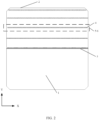
- FIG. 1 shows a pattern of laser spots of an SE according to one or more embodiments of the present disclosure
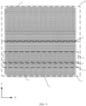
- FIG. 2 shows a pattern of laser spots of another SE according to one or more embodiments of the present disclosure, to describe a method for improving alignment between an SE and metal printing.
- the method includes: providing a silicon wafer 1, the silicon wafer 1 includes a first edge 2 and a midline 3, the midline 3 is parallel to the first edge 2; texturing and diffusing a surface of the silicon wafer 1; illuminating the surface of the silicon wafer 1 by laser spots 4 to form the selected emitter, between the first edge 2 and the midline 3, a plurality of the laser spots 4 is arranged along a first direction X to form spot rows 5, extension directions of the spot rows 5 are parallel to an extension direction of the first edge 2, M spot rows 5 are arranged along a second direction Y, M is a positive integer and M>1, the second direction Y intersects with the first direction X; the M spot rows 5 includes N sub-spot regions 6 arranged along the second direction, N is a positive integer and 1 ⁇ N ⁇ M, the sub-spot regions 6 includes at least one of the spot rows 5, and areas of the laser spots 4 in each of the sub-spot regions 6 are equal; and gradually increasing the areas of the laser spots 4 in different sub-spot
- the midline 3 herein is not an actual line on the silicon wafer 1.
- the midline 3 is a dummy line.
- a silicon wafer 1 is provided, and the silicon wafer 1 may be monocrystalline silicon, polycrystalline silicon, or amorphous silicon. In some embodiments, monocrystalline silicon is adopted.
- the surface of the silicon wafer 1 is textured and diffused. Prior to the texturing, the surface of the silicon wafer 1 is cleaned to remove impurities from the surface of the silicon wafer 1.
- a pyramid structure is formed on the surface of the silicon wafer 1 during the texturing, so as to reduce reflectivity of the surface of the silicon wafer 1.
- the textured silicon wafer 1 is diffused to form a PN junction.
- the diffused silicon wafer 1 is heavily doped by using laser spots 4. Areas of the laser spots 4 determine the size of the SE.
- FIG. 1 and FIG. 2 illustrate only a pattern of laser spots 4 between the first edge 2 and the midline 3.
- each sub-spot region 6 includes at least two spot rows 5, and FIG. 2 only illustrates that each sub-spot region 6 includes only one spot row 5, which is not limited thereto.
- the number of the sub-spot region 6, the number of the spot row 5 included in the sub-spot region 6, the number of the laser spots 4 included in the spot row 5, an interval between two adjacent laser spots 4, a spacing between two adjacent spot rows 5, and a spacing between two adjacent sub-spot regions 6 in FIG. 1 and FIG. 2 are merely illustrative, and are not limited thereto.
- one part of the sub-spot regions 6 include only one spot row 5, while the other part of the sub-spot regions 6 include at least two spot rows 5, which is not limited in the present disclosure, provided that the areas of the laser spots 4 in different sub-spot regions 6 are gradually increased along the direction from the midline 3 pointing to the first edge 2. The closer to the edge position of the silicon wafer 1, the larger the area of the laser spot 4, which is helpful to realize accurate alignment between the metal electrode and the SE when the metal electrode deviates greatly.
- the method for improving alignment between an SE and metal printing according to the present disclosure has at least the following advantages.
- a plurality of the laser spots 4 are arranged along a first direction X to form spot rows 5, extension directions of the spot rows 5 are parallel to an extension direction of the first edge 2, M spot rows 5 are arranged along a second direction Y, where M is a positive integer and M>1, and the second direction Y intersects with the first direction X.
- the M spot rows 5 include N sub-spot regions 6 arranged along the second direction Y, where N is a positive integer and 1 ⁇ N ⁇ M.
- the sub-spot regions 6 include at least one of the spot rows 5, and areas of the laser spots 4 in each of the sub-spot regions 6 are equal.
- the areas of the laser spots 4 in different sub-spot regions 6 are gradually increased along a direction in which the midline 3 points to the first edge 2.
- the metal electrode is generally printed by a screen. Due to bonding of hot melt adhesive at edges of the screen and prolonging of the service life, the metal electrode at an edge position may deviate. That is, the position of the metal electrode at the edge changes greatly, while the position of the metal electrode in the middle changes little. Therefore, by designing the area of the laser spot 4 at a middle position to be small and the area of the laser spot 4 at an edge position to be large, contact resistance of contact between the silicon wafer 1 and the SE at the middle position can be reduced, a fill factor can be increased, and efficiency of a solar cell can be improved. Besides, when the service life of the screen is prolonged, the metal electrode at the edge position and the SE at the edge position are accurately aligned.
- each sub-spot region 6 includes only one spot row 5.
- each sub-spot region 6 includes only one spot row 5, areas of the laser spots 4 in each sub-spot region 6 are equal, and the areas of the laser spots 4 in different sub-spot regions 6 are gradually increased along a direction from the midline 3 pointing to the first edge 2. That is, the areas of the laser spots 4 of each spot row 5 are gradually increased along the direction from the midline 3 pointing to the first edge 2.
- the gradient areas of the laser spots 4 can further adapt to gradual deviation of the metal electrode and ensure accuracy of the alignment between the metal electrode and the SE, and can also ensure reduction of the contact resistance of the contact between the silicon wafer 1 and the SE at the middle position, increase of the fill factor, and thereby improving the efficiency of the solar cell.
- each sub-spot region 6 includes at least two spot rows 5.
- each sub-spot region 6 includes at least two spot rows 5, areas of the laser spots 4 in each sub-spot region 6 are equal, and the areas of the laser spots 4 in different sub-spot regions 6 are gradually increased along the direction from the midline 3 pointing to the first edge 2. That is, sizes of the laser spots 4 are designed regionally along the direction from the midline 3 pointing to the first edge 2, so as to more adapt to deviation of the metal electrode only at the edge position, which can ensure minimum contact resistance between the silicon wafer 1 and the SE at the middle position, thereby improving the efficiency of the solar cell.
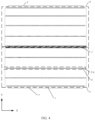
- FIG. 3 shows a pattern of laser spots of yet another SE according to one or more embodiments of the present disclosure
- FIG. 4 shows a pattern of laser spots of still another SE according to one or more embodiments of the present disclosure
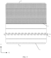
- FIG. 5 shows a pattern of laser spots of a further SE according to one or more embodiments of the present disclosure.
- the silicon wafer 1 further includes a second edge 7. The second edge 7 is arranged opposite to the first edge 2 along the second direction Y
- the plurality of laser spots 4 are arranged along the first direction X to form spot rows 5, and P spot rows 5 are arranged along the second direction Y, where P is a positive integer and P>1.
- the P spot rows 5 include Q sub-spot regions 6 arranged along the second direction Y, where Q is a positive integer and 1 ⁇ Q ⁇ P, the sub-spot regions 6 include at least one of the spot rows 5, and areas of the laser spots 4 in each of the sub-spot regions 6 are equal.
- the areas of the laser spots 4 in the sub-spot regions 6 are gradually increased along a direction from the midline 3 pointing to the second edge 7.
- FIG. 3 only illustrates that each sub-spot region 6 includes at least two spot rows 5 between the second edge 7 and the midline 3
- FIG. 4 and FIG. 5 only illustrate that each sub-spot region includes only one spot row 5 between the second edge 7 and the midline 3. That is, a pattern of the laser spots 4 between the first edge 2 and the midline 3 is different from a pattern of the laser spots 4 between the second edge 7 and the midline 3, which is not limited thereto.
- one part of the sub-spot regions 6 include only one spot row 5, while the other part of the sub-spot regions 6 include at least two spot rows 5, which is not limited in the present disclosure.
- the areas of the laser spots 4 in the sub-spot regions 6 are gradually increased along the direction from the midline 3 pointing to the first edge 2, and the areas of the laser spots 4 in the sub-spot regions 6 are gradually increased along the direction from the midline 3 pointing to the second edge 7.
- the metal electrodes at the first edge 2 and the second edge 7 both deviate, the metal electrodes at the first edge 2 and the second edge 7 can accurately contact the SE, while the center of the silicon wafer 1 maintains small contact resistance with the SE.
- the laser spots 4 between the midline 3 and the first edge 2 form a first spot region 8
- the laser spots 4 between the midline 3 and the second edge 7 form a second spot region 9
- the first spot region 8 and the second spot region 9 are symmetric along the midline 3.
- the silicon wafer 1 is symmetric along the midline 3
- the symmetry of the first spot region 8 and the second spot region 9 along the midline 3 is more reasonable, brings a better alignment effect, and achieves higher efficiency of the solar cell.
- the laser spots 4 are circular.
- orthographic projections of the laser spots 4 on the silicon wafer 1 are circular, and the areas of the laser spots 4 can be changed by changing diameters of the laser spots 4.
- the laser spots 4 may also be rectangular, equilaterally polygonal, or the like.
- lengths and widths of the laser spots 4 can be increased simultaneously to increase the areas of the laser spots 4.
- the lengths and the widths of the laser spots 4 have a linear relationship.
- printing speeds of lasers on the silicon wafer 1, laser power, laser frequencies, and focal lengths of a lens through which the lasers are emitted are adjusted to adjust the diameters of the laser spots 4.
- the sizes of the laser spots 4 may be changed by changing relative positions of lenses in a device from which the lasers are emitted, or by cooperatively adjusting printing speeds, laser power, laser frequencies, and focal lengths of lenses through which the lasers are emitted.
- the focal lengths of the lenses through which the lasers are emitted may be adjusted by shifting positions of the lenses through which the lasers are emitted to change positions of focuses.
- the printing speed ranges from 20000 mm/s to 24000 mm/s
- the laser power ranges from 29 W to 31 W
- the laser frequency ranges from 230 KHZ to 270 KHZ
- the focal length ranges from 30000 mm to 38000 mm.
- the diameters of the laser spots 4 may be increased. That is, the laser spots 4 may be formed near the first edge 2 and/or the second edge 7 by using the above parameters.
- the printing speed ranges from 20000 mm/s to 24000 mm/s
- the laser power ranges from 28 W to 30 W
- the laser frequency ranges from 270 KHZ to 330 KHZ
- the focal length ranges from 28000 mm to 35000 mm.
- the diameters of the laser spots 4 formed are small. That is, the laser spots 4 may be formed near the midline 3 by using the above parameters.
- the diameters of the laser spots 4 range from 35 ⁇ m to 130 ⁇ m.
- the diameters of the laser spots 4 constantly increase along the midline 3 toward the first edge 2 and/or the second edge 7. That is, the diameters of the laser spots 4 near the midline 3 are 35 ⁇ m, and the diameters of the laser spots 4 near the first edge 2 and/or the second edge 7 are 130 ⁇ m.
- the diameters of the laser spots 4 near the midline 3 range from 50 ⁇ m to 60 ⁇ m, and the diameters of the laser spots 4 near the first edge 2 and/or the second edge 7 range from 85 ⁇ m to 100 ⁇ m.
- the method for improving alignment between an SE and metal printing according to the present disclosure achieves at least the following beneficial effects.
- a plurality of the laser spots are arranged along a first direction to form spot rows, extension directions of the spot rows are parallel to an extension direction of the first edge, M spot rows are arranged along a second direction, where M is a positive integer and M>1, and the second direction intersects with the first direction.
- the M spot rows include N sub-spot regions arranged along the second direction, where N is a positive integer and 1 ⁇ N ⁇ M, the sub-spot regions include at least one of the spot rows, and areas of the laser spots in each of the sub-spot regions are equal.
- the areas of the laser spots in different sub-spot regions are gradually increased along a direction in which the midline points to the first edge.
- the metal electrode is generally printed by a screen. Due to bonding of hot melt adhesive at edges of the screen and prolonging of the service life, the metal electrode at an edge position may deviate. That is, the position of the metal electrode at the edge changes greatly, while the position of the metal electrode in the middle changes little. Therefore, by designing the area of the laser spot at a middle position to be small and the area of the laser spot at an edge position to be large, contact resistance of contact between the silicon wafer and the SE at the middle position can be reduced, the fill factor can be increased, and efficiency of a solar cell can be improved. Besides, when the service life of the screen is prolonged, the metal electrode at the edge position and the SE at the edge position are accurately aligned.
Landscapes
- Crystals, And After-Treatments Of Crystals (AREA)
- Photovoltaic Devices (AREA)
- Laser Beam Processing (AREA)
- Manufacture Or Reproduction Of Printing Formes (AREA)
Abstract
Description
- The present disclosure relates to the technical field of solar cells, and in particular, to a method for improving alignment between a selective emitter (SE) and metal printing.
- In recent years, with the decline of fossil fuels and their negative impact on environments, research and utilization of solar energy as pollution-free and renewable energy have been rapidly developed.
- With the continuous development of the photovoltaic industry, a photovoltaic module has a greater demand for high-efficiency cells. In industrial production of the high-efficiency cells, an SE cell technology has been widely used. An SE cell has a structure featured with heavy doping in a screen metal electrode contact region and light doping in a screen metal electrode non-contact region by using lasers. The structure can reduce diffusion layer coincidence, improve a shortwave effect of optical fibers, and increase a short-circuit current and an open-circuit voltage.
- In the manufacturing process of the SE cell, it is inevitable to balance alignment between laser spots and screen metal electrodes. For example, if the laser spots are larger, the heavily doped region is larger, so it is easier to align the metal electrodes with the light spots. However, excessively large laser spots may affect the open-circuit voltage of the SE cell and reduce power generation efficiency of the SE cell. If the laser spots are smaller, higher precision of the alignment between the metal electrodes and the laser spots is required.
- Therefore, it is urgent to provide a method for improving alignment between an SE and metal printing.
- In view of the above, the present disclosure provides a method for improving alignment between an SE and metal printing, including: providing a silicon wafer including a first edge and a midline, the midline is parallel to the first edge; texturing and diffusing a surface of the silicon wafer; and illuminating the surface of the silicon wafer by laser spots to form the SE. A plurality of the laser spots are arranged along a first direction between the first edge and the midline to form spot rows, extension directions of the spot rows are parallel to an extension direction of the first edge, M spot rows are arranged along a second direction intersecting with the first direction, and M is a positive integer and M>1. The M spot rows include N sub-spot regions arranged along the second direction, N is a positive integer and 1<N≤M, the sub-spot regions include at least one of the spot rows, and areas of the laser spots in each of the sub-spot regions are equal. The areas of the laser spots in different sub-spot regions along a direction from the midline pointing to the first edge gradually increases.
- Other features of the present disclosure and advantages thereof will become clear from the following detailed description of exemplary embodiments of the present disclosure with reference to the accompanying drawings.
- The accompanying drawings, which are incorporated in and constitute a part of the specification, illustrate embodiments of the present disclosure and, together with the description, serve to explain the principles of the present disclosure.
-
FIG. 1 shows a pattern of laser spots of an SE according to one or more embodiments of the present disclosure; -
FIG. 2 shows a pattern of laser spots of another SE according to one or more embodiments of the present disclosure; -
FIG. 3 shows a pattern of laser spots of yet another SE according to one or more embodiments of the present disclosure; -
FIG. 4 shows a pattern of laser spots of still another SE according to one or more embodiments of the present disclosure; and -
FIG. 5 shows a pattern of laser spots of a further SE according to one or more embodiments of the present disclosure. - Various exemplary embodiments of the present disclosure are now described in detail with reference to the accompanying drawings. It should be noted that, unless otherwise stated specifically, relative arrangement of the components and order of steps, the numerical expressions, and the values set forth in the embodiments are not intended to limit the scope of the present disclosure.
- The following description of one or more exemplary embodiments is in fact merely illustrative, and shall not be construed as any limitations on the present disclosure and application or use thereof.
- Technologies, methods, and devices known to those of ordinary skill in the related art may not be discussed in detail, but where appropriate, such technologies, methods, and devices should be considered as part of the specification. In all the examples shown and discussed herein, any specific value should be construed as merely illustrative and not as any limitation. Therefore, other examples of exemplary embodiments may have different values.
- It should be noted that similar reference signs and letters denote similar terms in the accompanying drawings, and therefore, once an item is defined in a drawing, there is no need for further discussion in the accompanying drawings.
- Referring to
FIG. 1 andFIG. 2 ,FIG. 1 shows a pattern of laser spots of an SE according to one or more embodiments of the present disclosure, andFIG. 2 shows a pattern of laser spots of another SE according to one or more embodiments of the present disclosure, to describe a method for improving alignment between an SE and metal printing. The method includes: providing asilicon wafer 1, thesilicon wafer 1 includes afirst edge 2 and amidline 3, themidline 3 is parallel to thefirst edge 2; texturing and diffusing a surface of thesilicon wafer 1; illuminating the surface of thesilicon wafer 1 bylaser spots 4 to form the selected emitter, between thefirst edge 2 and themidline 3, a plurality of thelaser spots 4 is arranged along a first direction X to formspot rows 5, extension directions of thespot rows 5 are parallel to an extension direction of thefirst edge 2,M spot rows 5 are arranged along a second direction Y, M is a positive integer and M>1, the second direction Y intersects with the first direction X; theM spot rows 5 includesN sub-spot regions 6 arranged along the second direction, N is a positive integer and 1<N≤M, thesub-spot regions 6 includes at least one of thespot rows 5, and areas of thelaser spots 4 in each of thesub-spot regions 6 are equal; and gradually increasing the areas of thelaser spots 4 indifferent sub-spot regions 6 along a direction from themidline 3 pointing to thefirst edge 2. - It is to be noted that the
midline 3 herein is not an actual line on thesilicon wafer 1. Themidline 3 is a dummy line. Asilicon wafer 1 is provided, and thesilicon wafer 1 may be monocrystalline silicon, polycrystalline silicon, or amorphous silicon. In some embodiments, monocrystalline silicon is adopted. The surface of thesilicon wafer 1 is textured and diffused. Prior to the texturing, the surface of thesilicon wafer 1 is cleaned to remove impurities from the surface of thesilicon wafer 1. A pyramid structure is formed on the surface of thesilicon wafer 1 during the texturing, so as to reduce reflectivity of the surface of thesilicon wafer 1. Thetextured silicon wafer 1 is diffused to form a PN junction. The diffusedsilicon wafer 1 is heavily doped by usinglaser spots 4. Areas of thelaser spots 4 determine the size of the SE. - It may be understood that, referring to
FIG. 1 andFIG. 2 ,FIG. 1 andFIG. 2 illustrate only a pattern oflaser spots 4 between thefirst edge 2 and themidline 3. InFIG. 1 , eachsub-spot region 6 includes at least twospot rows 5, andFIG. 2 only illustrates that eachsub-spot region 6 includes only onespot row 5, which is not limited thereto. The number of thesub-spot region 6, the number of thespot row 5 included in thesub-spot region 6, the number of thelaser spots 4 included in thespot row 5, an interval between twoadjacent laser spots 4, a spacing between twoadjacent spot rows 5, and a spacing between twoadjacent sub-spot regions 6 inFIG. 1 andFIG. 2 are merely illustrative, and are not limited thereto. Alternatively, one part of thesub-spot regions 6 include only onespot row 5, while the other part of thesub-spot regions 6 include at least twospot rows 5, which is not limited in the present disclosure, provided that the areas of thelaser spots 4 indifferent sub-spot regions 6 are gradually increased along the direction from themidline 3 pointing to thefirst edge 2. The closer to the edge position of the silicon wafer 1, the larger the area of thelaser spot 4, which is helpful to realize accurate alignment between the metal electrode and the SE when the metal electrode deviates greatly. - Compared with the related art, the method for improving alignment between an SE and metal printing according to the present disclosure has at least the following advantages.
- In the method for improving alignment between an SE and metal printing according to the present disclosure, between the
first edge 2 and themidline 3, a plurality of thelaser spots 4 are arranged along a first direction X to formspot rows 5, extension directions of thespot rows 5 are parallel to an extension direction of thefirst edge 2,M spot rows 5 are arranged along a second direction Y, where M is a positive integer and M>1, and the second direction Y intersects with the first direction X. TheM spot rows 5 includeN sub-spot regions 6 arranged along the second direction Y, where N is a positive integer and 1<N≤M. Thesub-spot regions 6 include at least one of thespot rows 5, and areas of thelaser spots 4 in each of thesub-spot regions 6 are equal. The areas of thelaser spots 4 indifferent sub-spot regions 6 are gradually increased along a direction in which themidline 3 points to thefirst edge 2. The metal electrode is generally printed by a screen. Due to bonding of hot melt adhesive at edges of the screen and prolonging of the service life, the metal electrode at an edge position may deviate. That is, the position of the metal electrode at the edge changes greatly, while the position of the metal electrode in the middle changes little. Therefore, by designing the area of thelaser spot 4 at a middle position to be small and the area of thelaser spot 4 at an edge position to be large, contact resistance of contact between thesilicon wafer 1 and the SE at the middle position can be reduced, a fill factor can be increased, and efficiency of a solar cell can be improved. Besides, when the service life of the screen is prolonged, the metal electrode at the edge position and the SE at the edge position are accurately aligned. - In some embodiments, still referring to
FIG. 2 , eachsub-spot region 6 includes only onespot row 5. - It may be understood that each
sub-spot region 6 includes only onespot row 5, areas of thelaser spots 4 in eachsub-spot region 6 are equal, and the areas of thelaser spots 4 indifferent sub-spot regions 6 are gradually increased along a direction from themidline 3 pointing to thefirst edge 2. That is, the areas of thelaser spots 4 of eachspot row 5 are gradually increased along the direction from themidline 3 pointing to thefirst edge 2. The gradient areas of thelaser spots 4 can further adapt to gradual deviation of the metal electrode and ensure accuracy of the alignment between the metal electrode and the SE, and can also ensure reduction of the contact resistance of the contact between thesilicon wafer 1 and the SE at the middle position, increase of the fill factor, and thereby improving the efficiency of the solar cell. - In some embodiments, still referring to
FIG. 1 , eachsub-spot region 6 includes at least twospot rows 5. - It may be understood that each
sub-spot region 6 includes at least twospot rows 5, areas of thelaser spots 4 in eachsub-spot region 6 are equal, and the areas of thelaser spots 4 in differentsub-spot regions 6 are gradually increased along the direction from themidline 3 pointing to thefirst edge 2. That is, sizes of thelaser spots 4 are designed regionally along the direction from themidline 3 pointing to thefirst edge 2, so as to more adapt to deviation of the metal electrode only at the edge position, which can ensure minimum contact resistance between thesilicon wafer 1 and the SE at the middle position, thereby improving the efficiency of the solar cell. - In some embodiments, referring to
FIG. 3 ,FIG. 4 , andFIG. 5 ,FIG. 3 shows a pattern of laser spots of yet another SE according to one or more embodiments of the present disclosure,FIG. 4 shows a pattern of laser spots of still another SE according to one or more embodiments of the present disclosure, andFIG. 5 shows a pattern of laser spots of a further SE according to one or more embodiments of the present disclosure. Thesilicon wafer 1 further includes asecond edge 7. Thesecond edge 7 is arranged opposite to thefirst edge 2 along the second direction Y - Between the
second edge 7 and themidline 3, the plurality oflaser spots 4 are arranged along the first direction X to formspot rows 5, andP spot rows 5 are arranged along the second direction Y, where P is a positive integer and P>1. - The
P spot rows 5 include Qsub-spot regions 6 arranged along the second direction Y, where Q is a positive integer and 1<Q≤P, thesub-spot regions 6 include at least one of thespot rows 5, and areas of thelaser spots 4 in each of thesub-spot regions 6 are equal. - The areas of the
laser spots 4 in thesub-spot regions 6 are gradually increased along a direction from themidline 3 pointing to thesecond edge 7. - It may be understood that
FIG. 3 only illustrates that eachsub-spot region 6 includes at least twospot rows 5 between thesecond edge 7 and themidline 3, andFIG. 4 andFIG. 5 only illustrate that each sub-spot region includes only onespot row 5 between thesecond edge 7 and themidline 3. That is, a pattern of thelaser spots 4 between thefirst edge 2 and themidline 3 is different from a pattern of thelaser spots 4 between thesecond edge 7 and themidline 3, which is not limited thereto. Alternatively, between thesecond edge 7 and themidline 3, one part of thesub-spot regions 6 include only onespot row 5, while the other part of thesub-spot regions 6 include at least twospot rows 5, which is not limited in the present disclosure. The areas of thelaser spots 4 in thesub-spot regions 6 are gradually increased along the direction from themidline 3 pointing to thefirst edge 2, and the areas of thelaser spots 4 in thesub-spot regions 6 are gradually increased along the direction from themidline 3 pointing to thesecond edge 7. When the metal electrodes at thefirst edge 2 and thesecond edge 7 both deviate, the metal electrodes at thefirst edge 2 and thesecond edge 7 can accurately contact the SE, while the center of thesilicon wafer 1 maintains small contact resistance with the SE. - In some embodiments, still referring to
FIG. 3 andFIG. 4 , thelaser spots 4 between themidline 3 and thefirst edge 2 form afirst spot region 8, thelaser spots 4 between themidline 3 and thesecond edge 7 form a second spot region 9, and thefirst spot region 8 and the second spot region 9 are symmetric along themidline 3. - It may be understood that, since the
silicon wafer 1 is symmetric along themidline 3, the symmetry of thefirst spot region 8 and the second spot region 9 along themidline 3 is more reasonable, brings a better alignment effect, and achieves higher efficiency of the solar cell. - In some embodiments, still referring to
FIG. 1 to FIG. 5 , thelaser spots 4 are circular. - It may be understood that orthographic projections of the laser spots 4 on the
silicon wafer 1 are circular, and the areas of thelaser spots 4 can be changed by changing diameters of the laser spots 4. - In some embodiments, the
laser spots 4 may also be rectangular, equilaterally polygonal, or the like. When thelaser spots 4 are oblong, lengths and widths of thelaser spots 4 can be increased simultaneously to increase the areas of the laser spots 4. The lengths and the widths of thelaser spots 4 have a linear relationship. - In some embodiments, printing speeds of lasers on the
silicon wafer 1, laser power, laser frequencies, and focal lengths of a lens through which the lasers are emitted are adjusted to adjust the diameters of the laser spots 4. - It may be understood that the sizes of the
laser spots 4 may be changed by changing relative positions of lenses in a device from which the lasers are emitted, or by cooperatively adjusting printing speeds, laser power, laser frequencies, and focal lengths of lenses through which the lasers are emitted. The focal lengths of the lenses through which the lasers are emitted may be adjusted by shifting positions of the lenses through which the lasers are emitted to change positions of focuses. - In some embodiments, for the
laser spot 4 far from themidline 3, the printing speed ranges from 20000 mm/s to 24000 mm/s, the laser power ranges from 29 W to 31 W, the laser frequency ranges from 230 KHZ to 270 KHZ, and the focal length ranges from 30000 mm to 38000 mm. - It may be understood that, by setting the above parameters, the diameters of the
laser spots 4 may be increased. That is, thelaser spots 4 may be formed near thefirst edge 2 and/or thesecond edge 7 by using the above parameters. - In some embodiments, for the
laser spot 4 close to themidline 3, the printing speed ranges from 20000 mm/s to 24000 mm/s, the laser power ranges from 28 W to 30 W, the laser frequency ranges from 270 KHZ to 330 KHZ, and the focal length ranges from 28000 mm to 35000 mm. - It may be understood that, by setting the above parameters, the diameters of the laser spots 4 formed are small. That is, the
laser spots 4 may be formed near themidline 3 by using the above parameters. - In some embodiments, the diameters of the
laser spots 4 range from 35 µm to 130 µm. - It may be understood that, the diameters of the
laser spots 4 constantly increase along themidline 3 toward thefirst edge 2 and/or thesecond edge 7. That is, the diameters of thelaser spots 4 near themidline 3 are 35 µm, and the diameters of thelaser spots 4 near thefirst edge 2 and/or thesecond edge 7 are 130 µm. - In some embodiments, the diameters of the
laser spots 4 near themidline 3 range from 50 µm to 60 µm, and the diameters of thelaser spots 4 near thefirst edge 2 and/or thesecond edge 7 range from 85 µm to 100 µm. - As can be known from the above embodiments, the method for improving alignment between an SE and metal printing according to the present disclosure achieves at least the following beneficial effects.
- In the method for improving alignment between an SE and metal printing according to the present disclosure, between the first edge and the midline, a plurality of the laser spots are arranged along a first direction to form spot rows, extension directions of the spot rows are parallel to an extension direction of the first edge, M spot rows are arranged along a second direction, where M is a positive integer and M>1, and the second direction intersects with the first direction. The M spot rows include N sub-spot regions arranged along the second direction, where N is a positive integer and 1<N≤M, the sub-spot regions include at least one of the spot rows, and areas of the laser spots in each of the sub-spot regions are equal. The areas of the laser spots in different sub-spot regions are gradually increased along a direction in which the midline points to the first edge. The metal electrode is generally printed by a screen. Due to bonding of hot melt adhesive at edges of the screen and prolonging of the service life, the metal electrode at an edge position may deviate. That is, the position of the metal electrode at the edge changes greatly, while the position of the metal electrode in the middle changes little. Therefore, by designing the area of the laser spot at a middle position to be small and the area of the laser spot at an edge position to be large, contact resistance of contact between the silicon wafer and the SE at the middle position can be reduced, the fill factor can be increased, and efficiency of a solar cell can be improved. Besides, when the service life of the screen is prolonged, the metal electrode at the edge position and the SE at the edge position are accurately aligned.
- Although some specific embodiments of the present disclosure have been described in detail through examples, it should be understood by those skilled in the art that the above examples are for illustrative purposes only and not intended to limit the scope of the present disclosure. The scope of the present disclosure is defined by the appended claims.
Claims (15)
- A method for improving alignment between a selective emitter (SE) and metal printing, comprising:providing a silicon wafer comprising a first edge and a midline, wherein the midline is parallel to the first edge;texturing and diffusing a surface of the silicon wafer; andilluminating the surface of the silicon wafer by laser spots to form the SE,wherein a plurality of the laser spots are arranged along a first direction between the first edge and the midline to form spot rows, extension directions of the spot rows are parallel to an extension direction of the first edge, M spot rows are arranged along a second direction intersecting with the first direction, and M is a positive integer and M>1;the M spot rows comprise N sub-spot regions arranged along the second direction, N is a positive integer and 1<N≤M, the sub-spot regions comprise at least one of the spot rows, and areas of the laser spots in each of the sub-spot regions are equal; andthe areas of the laser spots in different sub-spot regions along a direction from the midline pointing to the first edge gradually increases.
- The method for improving alignment between an SE and metal printing according to claim 1, wherein each of the sub-spot regions comprises only one of the spot rows.
- The method for improving alignment between an SE and metal printing according to claim 1, wherein each of the sub-spot regions comprises at least two of the spot rows.
- The method for improving alignment between an SE and metal printing according to claim 1, wherein the silicon wafer further comprises a second edge arranged opposite to the first edge along the second direction;wherein the plurality of laser spots are arranged along the first direction between the second edge and the midline to form spot rows, P spot rows are arranged along the second direction, and P is a positive integer and P>1;the P spot rows comprise Q sub-spot regions arranged along the second direction, Q is a positive integer and 1<Q≤P, the sub-spot regions comprise at least one of the spot rows, and areas of the laser spots in each of the sub-spot regions are equal; andthe areas of the laser spots in the sub-spot regions along a direction from the midline pointing to the second edge gradually increases.
- The method for improving alignment between an SE and metal printing according to claim 4, wherein the laser spots between the midline and the first edge form a first spot region, the laser spots between the midline and the second edge form a second spot region, and the first spot region and the second spot region are symmetric along the midline.
- The method for improving alignment between an SE and metal printing according to claim 1, wherein the laser spots have a circular shape.
- The method for improving alignment between an SE and metal printing according to claim 6, wherein printing speeds of lasers on the silicon wafer, laser power, laser frequencies, and focal lengths of a lens through which the lasers are emitted are adjusted to adjust diameters of the laser spots.
- The method for improving alignment between an SE and metal printing according to claim 7, wherein, for the laser spot far from the midline, the printing speed ranges from 20000 mm/s to 24000 mm/s, the laser power ranges from 29 W to 31 W, the laser frequency ranges from 230 KHZ to 270 KHZ, and the focal length ranges from 30000 mm to 38000 mm.
- The method for improving alignment between an SE and metal printing according to claim 7, wherein, for the laser spot close to the midline, the printing speed ranges from 20000 mm/s to 24000 mm/s, the laser power ranges from 28 W to 30 W, the laser frequency ranges from 270 KHZ to 330 KHZ, and the focal length ranges from 28000 mm to 35000 mm.
- The method for improving alignment between an SE and metal printing according to claim 6, wherein the diameters of the laser spots range from 35 µm to 130 µm.
- The method for improving alignment between an SE and metal printing according to claim 10, wherein the diameters of the laser spots adjacent to the midline range from 50 µm to 60 µm.
- The method for improving alignment between an SE and metal printing according to claim 10, wherein the diameters of the laser spots adjacent to the first edge and/or the second edge range from 85 µm to 100 µm.
- The method for improving alignment between an SE and metal printing according to claim 1, wherein the laser spots have a rectangular shape or a polygonal shape.
- The method for improving alignment between an SE and metal printing according to claim 1, further comprising:
forming a pyramid structure on a surface of the silicon wafer during the texturing. - The method for improving alignment between an SE and metal printing according to claim 1, wherein the silicon wafer is monocrystalline silicon, polycrystalline silicon, or amorphous silicon.
Applications Claiming Priority (1)
| Application Number | Priority Date | Filing Date | Title |
|---|---|---|---|
| CN202210892920.3A CN115249751B (en) | 2022-07-27 | 2022-07-27 | Method for Improving Selective Emitter Alignment with Metal Printing |
Publications (2)
| Publication Number | Publication Date |
|---|---|
| EP4312280A1 true EP4312280A1 (en) | 2024-01-31 |
| EP4312280B1 EP4312280B1 (en) | 2026-04-15 |
Family
ID=83693158
Family Applications (1)
| Application Number | Title | Priority Date | Filing Date |
|---|---|---|---|
| EP22201297.3A Active EP4312280B1 (en) | 2022-07-27 | 2022-10-13 | Method for improving alignment between selective emitter and metal printing |
Country Status (5)
| Country | Link |
|---|---|
| US (1) | US12419130B2 (en) |
| EP (1) | EP4312280B1 (en) |
| JP (1) | JP7393496B1 (en) |
| CN (1) | CN115249751B (en) |
| AU (1) | AU2022252768A1 (en) |
Families Citing this family (1)
| Publication number | Priority date | Publication date | Assignee | Title |
|---|---|---|---|---|
| CN116722077A (en) * | 2023-06-28 | 2023-09-08 | 滁州捷泰新能源科技有限公司 | SE structure preparation method and solar cell |
Citations (5)
| Publication number | Priority date | Publication date | Assignee | Title |
|---|---|---|---|---|
| CN109065658A (en) * | 2018-07-12 | 2018-12-21 | 浙江爱旭太阳能科技有限公司 | A kind of p-type SE-PERC double-sided solar battery and preparation method thereof |
| CN111180530A (en) * | 2019-12-27 | 2020-05-19 | 天津爱旭太阳能科技有限公司 | A kind of preparation method of selective emitter battery |
| CN112259621A (en) * | 2020-11-11 | 2021-01-22 | 通威太阳能(安徽)有限公司 | High-efficiency PERC solar cell and preparation method thereof |
| CN113782425A (en) * | 2021-09-01 | 2021-12-10 | 浙江爱旭太阳能科技有限公司 | Method for making a solar cell and solar cell |
| CN113903818A (en) * | 2021-11-05 | 2022-01-07 | 通威太阳能(成都)有限公司 | SE laser doping pattern of PERC battery and preparation method of PERC battery |
Family Cites Families (27)
| Publication number | Priority date | Publication date | Assignee | Title |
|---|---|---|---|---|
| US9508886B2 (en) * | 2007-10-06 | 2016-11-29 | Solexel, Inc. | Method for making a crystalline silicon solar cell substrate utilizing flat top laser beam |
| EP2441546B1 (en) * | 2010-10-12 | 2013-04-24 | Innovavent GmbH | Method and apparatus to form selective emitter areas on a solar cell |
| TW201234626A (en) | 2011-01-13 | 2012-08-16 | Intevac Inc | Non-contacting bus bars for solar cells and methods of making non-contacting bus bars |
| EP2654090B1 (en) | 2012-04-17 | 2020-07-08 | LG Electronics, Inc. | Solar cell |
| JP2014007188A (en) | 2012-06-21 | 2014-01-16 | Mitsubishi Electric Corp | Method of manufacturing solar battery |
| KR101921738B1 (en) * | 2012-06-26 | 2018-11-23 | 엘지전자 주식회사 | Solar cell |
| US9431563B2 (en) * | 2012-12-28 | 2016-08-30 | Kyocera Corporation | Solar cell element and method for manufacturing solar cell element |
| WO2014179368A1 (en) * | 2013-04-29 | 2014-11-06 | Solexel, Inc. | Damage free laser patterning of transparent layers for forming doped regions on a solar cell substrate |
| WO2015068247A1 (en) | 2013-11-07 | 2015-05-14 | 三菱電機株式会社 | Solar cell, manufacturing method therefor, and solar-cell module |
| CN107112373A (en) * | 2014-12-30 | 2017-08-29 | 默克专利股份有限公司 | Laser Doping of Semiconductors |
| CN107112381A (en) | 2014-12-30 | 2017-08-29 | 默克专利股份有限公司 | The method of doped semiconductor |
| US9673341B2 (en) * | 2015-05-08 | 2017-06-06 | Tetrasun, Inc. | Photovoltaic devices with fine-line metallization and methods for manufacture |
| US20180254359A1 (en) | 2015-08-28 | 2018-09-06 | Mitsubishi Electric Corporation | Solar cell and solar cell manufacturing method |
| CN206921831U (en) * | 2017-03-03 | 2018-01-23 | 广东爱旭科技股份有限公司 | P-type PERC double-sided solar cell and its components and systems |
| WO2018236885A1 (en) * | 2017-06-20 | 2018-12-27 | Natcore Technology, Inc. | SYSTEM AND METHODS FOR FORMING SINGLE-CONTACT BACK-EMITTING SOLAR CELLS WITH SELECTIVE CONTACTS OF CARRIERS |
| CN109038866A (en) * | 2018-07-03 | 2018-12-18 | 山东航天电子技术研究所 | A kind of laser radio biography energy emitting-receiving system |
| CN110379884B (en) * | 2019-06-05 | 2021-07-20 | 晶澳太阳能有限公司 | A kind of laser positioning point on battery surface and preparation method of PERC battery |
| CN110729381B (en) * | 2019-10-28 | 2021-04-27 | 浙江正泰太阳能科技有限公司 | Laser SE structure pattern fabrication method, device, equipment and storage medium |
| CN112531035B (en) * | 2020-12-03 | 2022-04-29 | 通威太阳能(成都)有限公司 | Solar cell and preparation method thereof, and multilayer composite passivation film on the back of solar cell |
| CN112599639A (en) * | 2020-12-15 | 2021-04-02 | 东莞南玻光伏科技有限公司 | Laser SE processing method of solar cell |
| CN112563347A (en) * | 2020-12-25 | 2021-03-26 | 通威太阳能(成都)有限公司 | PERC solar cell selective emitter, PERC solar cell and method of making the same |
| CN112736146A (en) | 2020-12-31 | 2021-04-30 | 湖南红太阳新能源科技有限公司 | PERC battery based on point contact and composite film layer |
| CN214336726U (en) * | 2021-02-19 | 2021-10-01 | 宁夏隆基乐叶科技有限公司 | A selective emitter pattern and solar cell sheet |
| CN215771135U (en) * | 2021-03-24 | 2022-02-08 | 浙江爱旭太阳能科技有限公司 | Laser marking structure of solar cell, laser marking and solar cell |
| CN114242812B (en) * | 2021-11-16 | 2025-12-19 | 晶澳太阳能有限公司 | Method for detecting doping effect of selective emitter of silicon-based solar cell |
| CN216488095U (en) * | 2021-11-24 | 2022-05-10 | 盐城阿特斯阳光能源科技有限公司 | Selective emitter solar cells and photovoltaic modules |
| CN114393298B (en) * | 2021-12-24 | 2024-10-18 | 通威太阳能(眉山)有限公司 | SE-PERC cell laser spot, SE-PERC cell square resistance modulation method and system |
-
2022
- 2022-07-27 CN CN202210892920.3A patent/CN115249751B/en active Active
- 2022-10-13 AU AU2022252768A patent/AU2022252768A1/en not_active Abandoned
- 2022-10-13 EP EP22201297.3A patent/EP4312280B1/en active Active
- 2022-10-18 US US17/968,497 patent/US12419130B2/en active Active
- 2022-10-19 JP JP2022167418A patent/JP7393496B1/en active Active
Patent Citations (5)
| Publication number | Priority date | Publication date | Assignee | Title |
|---|---|---|---|---|
| CN109065658A (en) * | 2018-07-12 | 2018-12-21 | 浙江爱旭太阳能科技有限公司 | A kind of p-type SE-PERC double-sided solar battery and preparation method thereof |
| CN111180530A (en) * | 2019-12-27 | 2020-05-19 | 天津爱旭太阳能科技有限公司 | A kind of preparation method of selective emitter battery |
| CN112259621A (en) * | 2020-11-11 | 2021-01-22 | 通威太阳能(安徽)有限公司 | High-efficiency PERC solar cell and preparation method thereof |
| CN113782425A (en) * | 2021-09-01 | 2021-12-10 | 浙江爱旭太阳能科技有限公司 | Method for making a solar cell and solar cell |
| CN113903818A (en) * | 2021-11-05 | 2022-01-07 | 通威太阳能(成都)有限公司 | SE laser doping pattern of PERC battery and preparation method of PERC battery |
Also Published As
| Publication number | Publication date |
|---|---|
| CN115249751B (en) | 2023-08-29 |
| CN115249751A (en) | 2022-10-28 |
| US20240038923A1 (en) | 2024-02-01 |
| US12419130B2 (en) | 2025-09-16 |
| JP2024018841A (en) | 2024-02-08 |
| JP7393496B1 (en) | 2023-12-06 |
| AU2022252768A1 (en) | 2024-02-15 |
| EP4312280B1 (en) | 2026-04-15 |
Similar Documents
| Publication | Publication Date | Title |
|---|---|---|
| AU2024204865B2 (en) | Solar cell and manufacturing method thereof, photovoltaic module, and photovoltaic system | |
| KR102195595B1 (en) | P-type PERC double-sided solar cell and its module, system and manufacturing method | |
| KR102323459B1 (en) | P-type PERC double-sided solar cell and its module, system and manufacturing method | |
| JP2010528483A (en) | Method for obtaining textured substrates for photovoltaic panels | |
| KR102323458B1 (en) | P-type PERC double-sided solar cell and its module, system and manufacturing method | |
| US10964828B2 (en) | Bifacial P-type PERC solar cell and module, system, and preparation method thereof | |
| CN101943765B (en) | Condenser lens, multocular lens condenser and multocular condenser solar cell assembly | |
| US20230361238A1 (en) | Method for manufacturing monocrystalline silicon wafer containing arced side, method for manufacturing monocrystalline silicon cell, and photovoltaic module | |
| EP4312280B1 (en) | Method for improving alignment between selective emitter and metal printing | |
| FR3131804A3 (en) | SOLAR MODULE | |
| AU2022268276B2 (en) | Solar module | |
| CN120051065B (en) | A back contact battery and photovoltaic module | |
| CN113851410A (en) | Battery piece printing alignment method | |
| CN222440597U (en) | SE-TOPCon battery | |
| CN201859887U (en) | fly's eye light-focusing solar battery component | |
| CN101937937B (en) | Compound eye type concentrator solar cell assembly and manufacturing process thereof | |
| CN109888058B (en) | Solar cell and manufacturing method thereof | |
| CN216354236U (en) | SE battery piece and photovoltaic module | |
| CN209357734U (en) | PERC battery and photovoltaic module | |
| CN221977194U (en) | A spot shaping device for laser processing | |
| CN223168617U (en) | Solar cell and cell module | |
| CN222750801U (en) | TOPCon-SE Solar Cell | |
| CN210443567U (en) | Laser grooving structure of back passivation solar cell | |
| US20120291864A1 (en) | Solar cell and solar cell fabrication method | |
| CN114975647A (en) | N-type back contact solar cell and preparation method thereof |
Legal Events
| Date | Code | Title | Description |
|---|---|---|---|
| PUAI | Public reference made under article 153(3) epc to a published international application that has entered the european phase |
Free format text: ORIGINAL CODE: 0009012 |
|
| STAA | Information on the status of an ep patent application or granted ep patent |
Free format text: STATUS: REQUEST FOR EXAMINATION WAS MADE |
|
| 17P | Request for examination filed |
Effective date: 20221013 |
|
| AK | Designated contracting states |
Kind code of ref document: A1 Designated state(s): AL AT BE BG CH CY CZ DE DK EE ES FI FR GB GR HR HU IE IS IT LI LT LU LV MC ME MK MT NL NO PL PT RO RS SE SI SK SM TR |
|
| RIN1 | Information on inventor provided before grant (corrected) |
Inventor name: LUO, FANGYAN Inventor name: QIU, YANKAI Inventor name: ZHANG, NING Inventor name: FEI, ZHILIANG |
|
| REG | Reference to a national code |
Ref country code: DE Free format text: PREVIOUS MAIN CLASS: H01L0031180000 Ref country code: DE Ref legal event code: R079 Ref document number: 602022034497 Country of ref document: DE Free format text: PREVIOUS MAIN CLASS: H01L0031180000 Ipc: H10F0010140000 |
|
| GRAP | Despatch of communication of intention to grant a patent |
Free format text: ORIGINAL CODE: EPIDOSNIGR1 |
|
| STAA | Information on the status of an ep patent application or granted ep patent |
Free format text: STATUS: GRANT OF PATENT IS INTENDED |
|
| RIC1 | Information provided on ipc code assigned before grant |
Ipc: H10F 10/14 20250101AFI20260107BHEP Ipc: H10F 71/00 20250101ALI20260107BHEP Ipc: H10F 77/20 20250101ALI20260107BHEP |
|
| INTG | Intention to grant announced |
Effective date: 20260116 |
|
| RAP3 | Party data changed (applicant data changed or rights of an application transferred) |
Owner name: ZHEJIANG JINKO SOLAR CO., LTD. Owner name: JINKO SOLAR CO., LTD. |
|
| GRAS | Grant fee paid |
Free format text: ORIGINAL CODE: EPIDOSNIGR3 |
|
| GRAA | (expected) grant |
Free format text: ORIGINAL CODE: 0009210 |
|
| STAA | Information on the status of an ep patent application or granted ep patent |
Free format text: STATUS: THE PATENT HAS BEEN GRANTED |
|
| AK | Designated contracting states |
Kind code of ref document: B1 Designated state(s): AL AT BE BG CH CY CZ DE DK EE ES FI FR GB GR HR HU IE IS IT LI LT LU LV MC ME MK MT NL NO PL PT RO RS SE SI SK SM TR |
|
| REG | Reference to a national code |
Ref country code: CH Ref legal event code: F10 Free format text: ST27 STATUS EVENT CODE: U-0-0-F10-F00 (AS PROVIDED BY THE NATIONAL OFFICE) Effective date: 20260415 |