EP4311379A1 - Multi-beam chip integration module and phased array system - Google Patents
Multi-beam chip integration module and phased array system Download PDFInfo
- Publication number
- EP4311379A1 EP4311379A1 EP22794244.8A EP22794244A EP4311379A1 EP 4311379 A1 EP4311379 A1 EP 4311379A1 EP 22794244 A EP22794244 A EP 22794244A EP 4311379 A1 EP4311379 A1 EP 4311379A1
- Authority
- EP
- European Patent Office
- Prior art keywords
- chips
- printed board
- board
- type chips
- chip
- Prior art date
- Legal status (The legal status is an assumption and is not a legal conclusion. Google has not performed a legal analysis and makes no representation as to the accuracy of the status listed.)
- Granted
Links
Images


Classifications
-
- H—ELECTRICITY
- H01—ELECTRIC ELEMENTS
- H01Q—ANTENNAS, i.e. RADIO AERIALS
- H01Q1/00—Details of, or arrangements associated with, antennas
- H01Q1/12—Supports; Mounting means
- H01Q1/22—Supports; Mounting means by structural association with other equipment or articles
- H01Q1/2283—Supports; Mounting means by structural association with other equipment or articles mounted in or on the surface of a semiconductor substrate as a chip-type antenna or integrated with other components into an IC package
-
- H—ELECTRICITY
- H05—ELECTRIC TECHNIQUES NOT OTHERWISE PROVIDED FOR
- H05K—PRINTED CIRCUITS; CASINGS OR CONSTRUCTIONAL DETAILS OF ELECTRIC APPARATUS; MANUFACTURE OF ASSEMBLAGES OF ELECTRICAL COMPONENTS
- H05K1/00—Printed circuits
- H05K1/18—Printed circuits structurally associated with non-printed electric components
- H05K1/181—Printed circuits structurally associated with non-printed electric components associated with surface mounted components
-
- H—ELECTRICITY
- H01—ELECTRIC ELEMENTS
- H01Q—ANTENNAS, i.e. RADIO AERIALS
- H01Q21/00—Antenna arrays or systems
- H01Q21/0006—Particular feeding systems
-
- H—ELECTRICITY
- H01—ELECTRIC ELEMENTS
- H01Q—ANTENNAS, i.e. RADIO AERIALS
- H01Q21/00—Antenna arrays or systems
- H01Q21/06—Arrays of individually energised antenna units similarly polarised and spaced apart
- H01Q21/061—Two dimensional planar arrays
-
- H—ELECTRICITY
- H01—ELECTRIC ELEMENTS
- H01Q—ANTENNAS, i.e. RADIO AERIALS
- H01Q25/00—Antennas or antenna systems providing at least two radiating patterns
- H01Q25/002—Antennas or antenna systems providing at least two radiating patterns providing at least two patterns of different beamwidth; Variable beamwidth antennas
-
- H—ELECTRICITY
- H01—ELECTRIC ELEMENTS
- H01Q—ANTENNAS, i.e. RADIO AERIALS
- H01Q3/00—Arrangements for changing or varying the orientation or the shape of the directional pattern of the waves radiated from an antenna or antenna system
- H01Q3/26—Arrangements for changing or varying the orientation or the shape of the directional pattern of the waves radiated from an antenna or antenna system varying the relative phase or relative amplitude of energisation between two or more active radiating elements; varying the distribution of energy across a radiating aperture
-
- H—ELECTRICITY
- H01—ELECTRIC ELEMENTS
- H01Q—ANTENNAS, i.e. RADIO AERIALS
- H01Q21/00—Antenna arrays or systems
Definitions
- the present disclosure relates to the field of phased array antennas, and more particularly to a multi-beam chip integration module and a phased array system.
- Ka frequency band and a higher one may provide advantages of high-rate and high-capacity data transmission, but meanwhile, due to the continuous reduction of antenna array units, the size of the array continues to decrease, ushering in greater challenges in integration and miniaturization. Especially in multi-beam high-frequency band phased array antennas, the difficulties become even greater.
- embodiments of the present disclosure provide a multi-beam chip integration module, the multi-beam chip integration module comprising a first printed board, at least one set of first-type chips, and at least one set of second-type chips;
- the first-type chips are multi-beam channel chips, while the second-type chips are multi-beam synthesis network chips; the number of the multi-beam synthesis network chips is 1, and the number of the multi-beam channel chips is 4;
- power supply pins of each set of multi-beam channel chips are respectively connected to corresponding power supply channels in the first side of the first printed board, and control pins of each set of multi-beam channel chips are respectively connected to corresponding control channels in the first side of the first printed board.
- a power supply pin of the multi-beam synthesis network chip is connected to a corresponding power supply channel in the second side of the first printed board, and a control pin of the multi-beam synthesis network chip is connected to a corresponding control channel in the second side of the first printed board.
- phased array system comprising an antenna unit, a second printed board, and at least one set of multi-beam chip integration modules;
- the multi-beam chip integration module comprises a first printing board, at least one set of first-type chips, and at least one set of second-type chips; the at least one set of first-type chips is surface mounted to a first side of the first printing board; the at least one set of second-type chips is surface mounted to a second side of the first printing board; the second side of the first printing board is an opposite side parallel to the first side of the first printing board;
- the first-type chips are multi-beam channel chips, while the second-type chips are multi-beam synthesis network chips; the number of the multi-beam synthesis network chips is 1, and the number of the multi-beam channel chips is 4;
- the second printed board is provided with an antenna feed network
- radio frequency signal channels in the first printed board are respectively connected to access points of the antenna feed network
- output points of the antenna feed network are respectively connected to different antenna units.
- radio frequency signal channels in the first printed board are respectively connected to access points of the antenna feed network via solder joints, the solder joints having a cross-sectional diameter greater than a thickness of the multi-beam synthesis network chip.
- the phased array system further comprises a heat dissipation module, one side of the heat dissipation module abutting against the first-type chips.
- embodiments of the present disclosure provide a multi-beam chip integration module and a phased array system, wherein the multi-beam chip integration module comprises a first printing board, at least one set of first-type chips, and at least one set of second-type chips, the at least one set of first-type chips surface mounted to a first side of the first printing board, and the at least one set of second-type chips surface mounted to a second side of the first printing board, and wherein the second side of the first printing board is an opposite side parallel to the first side of the first printing board.
- the chip layout following the reduced size of the printed board can be satisfied, the wiring complexity of the antenna network can be reduced, and the chip layout can be completed in a simple and rapid manner.
- Reference numbers in the figures include: 10-multi-beam chip integration module; 101-first-type chip; 102-second-type chip; 103-first printed board; 20-second printed board; 30-antenna unit; 40-heat dissipation module; 50-solder joint; 60-antenna feed network.
- the terms "provided” and “connected” and the like are to be understood in a broad sense.
- it may be a fixed connection, a detachable connection, or an integral connection; it may be a mechanical connection or an electrical connection; it may be a direct connection, or an indirect connection through an intermediary, or an internal communication of two elements.
- the specific meanings of these terms in the present disclosure may be understood in specific contexts.
- the existing multi-beam phased array antennas may be divided into analog multi-beam phased array antennas and digital multi-beam phased array antennas according to the beam formation.
- Analog multi-beam phased array antennas can implement multiple beams without reducing the signal-to-noise ratio received by the antennas, and the solution is simple and feasible, but requires too much hardware.
- Digital multi-beam phased array antennas are to digitize intermediate frequency signals and implement software, which has higher requirements for algorithms and hardware.
- the commonly used dual-beam phased array antennas are generally analog dual-beam phased array antennas. There are not many research results for phased array antennas with more beams. Under the premise of ever increasing requirements for miniaturization and integration, it is very difficult to specifically implement the layout of a multi-beam high-frequency phased array.
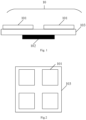
- FIG. 1 is a cross-sectional view of a multi-beam chip integration module 10 according to an embodiment of the present disclosure.
- the multi-beam chip integration module 10 includes a first printed board 103, at least one set of first-type chips 101, and at least one set of second-type chips 102.
- the at least one set of the first-type chips 101 is surface mounted to a first side of the first printed board 103.
- FIG. 2 is a top view of a multi-beam chip integration module 10 according to an embodiment of the present disclosure.
- the first-type chips 101 a resurface mounted to a first side of the first printed board 103.
- the number of the first-type chips 101 is shown as 4 in FIG. 2 , which is for ease of presentation and reference, and there is no limitation on the number of the first-type chips 101.
- the at least one set of second-type chips 102 is surface mounted to a second side of the first printed board 103.
- FIG. 3 shows a bottom view of a multi-beam chip integration module 10 according to an embodiment of the present disclosure.
- the second-type chips 102 a resurface mounted to the second side of the first printed board 103.
- the number of the second-type chips 102 is shown as 1 in FIG. 3 , which is for ease of presentation and reference, and there is no limitation on the number of the second-type chips 102.
- the chip layout following the reduced size of the printed board can be satisfied, the wiring complexity of the antenna network can be reduced, and the chip layout can be completed in a simple and rapid manner.
- the second side of the first printed board 103 is an opposite side that is parallel to the first side of the first printed board 103.
- embodiments of the present disclosure provide a multi-beam chip integration module, wherein the multi-beam chip integration module comprises a first printing board, at least one set of first-type chips, and at least one set of second-type chips, wherein the at least one set of first-type chips is surface mounted to a first side of the first printing board, wherein the at least one set of second-type chips is surface mounted to a second side of the first printing board, and wherein the second side of the first printing board is an opposite side parallel to the first side of the first printing board.
- the chip layout following the reduced size of the printed board can be satisfied, the wiring complexity of the antenna network can be reduced, and the chip layout can be completed in a simple and rapid manner.
- the first-type chips 101 are multi-beam channel chips
- the second-type chips 102 are multi-beam synthesis network chips
- the number of the multi-beam synthesis network chips is 1, and the number of the multi-beam channel chips is 4.
- Each set of multi-beam channel chips are respectively connected to different pins in the multi-beam synthesis network chip through different beam channels in the first printed board 103.
- the multi-beam channel chips and the multi-beam synthesis network chip are interconnected via a multilayer network constructed by beam channels of the first printed board 103.
- the multi-beam synthesis network chip is used to perform network synthesis or decomposition of input and output signals of the multi-beam channel chips.
- multi-beam synthesis network chips there are two layers of multi-beam synthesis network chips, wherein the multi-beam synthesis network chips of the lower layer are respectively connected to corresponding multi-beam channel chips, and the multi-beam synthesis network chips of the upper layer are respectively connected to an external control device and multi-beam synthesis network chips of the lower layer.
- multi-beam synthesis network chips of the upper layer are connected to an external control device and multi-beam synthesis network chips of the lower layer via corresponding pins in the first printed board 103.
- Signal pins in each set of multi-beam channel chips are respectively connected to different radio frequency signal channels in the first printed board 103, so as to be connected to corresponding antenna units.
- multi-beam channel chips may accomplish transceiving of radio frequency signals corresponding to antenna units through radio frequency signal channels.
- power supply pins of each set of multi-beam channel chips are respectively connected to corresponding power supply channels in the first side of the first printed board 103, and control pins of each set of multi-beam channel chips are respectively connected to corresponding control channels in the first side of the first printed board 103.
- a power supply pin of the multi-beam synthesis network chip is connected to a corresponding power supply channel in the second side of the first printed board 103, and a control pin of the multi-beam synthesis network chip is connected to a corresponding control channel in the second side of the first printed board 103.
- the first printed board 103 in the embodiment of the present disclosure is a printed circuit board fabricated via a Low Temperature Co-fired Ceramic (LTCC) process.
- LTCC Low Temperature Co-fired Ceramic
- Low-temperature co-fired ceramic process refers to a process of preparing low-temperature sintered ceramic powder into a green tape with a precise thickness and density as a circuit substrate material, subjecting the green tape to laser drilling, microporous grouting, and precision conductor paste printing and the like to form a desired circuit pattern, embedding a plurality of passive components therein, then laminating together, and sintering at 900°C to manufacture a passive integrated component of a three-dimensional circuit network, or to manufacture a three-dimensional circuit substrate with a built-in passive element, with an IC and an active device mounted on its surface to make a passive/active integrated functional module.
- Embodiments of the present disclosure further provide a phased array system comprising an antenna unit 30, a second printed board 20, and at least one set of multi-beam chip integration modules 10, as shown in FIG. 4 .
- a multi-beam chip integration module 10 includes a first printing board 103, at least one set of first-type chips 101, and at least one set of second-type chips 102; the at least one set of first-type chips 101 is surface mounted to a first side of the first printing board 103; the at least one set of second-type chips 102 is surface mounted to a second side of the first printing board 103; the second side of the first printing board 103 is an opposite side parallel to the first side of the first printing board 103.
- a second side of the multi-beam chip integration module 10 is surface mounted to one side of the second printed board 20, and the first printed board 103 and the second printed board 20 together define a hollow cavity, in which cavity the at least one set of the second-type chips 102 is disposed;
- the antenna unit 30 is surface mounted to the other side of the second printed board 20.
- the panel size of the printed board is reduced with the same number of antenna units 30 due to the reduced size of the antenna units 30 and the reduced spacing between the antenna units 30.
- surface mounting the first-type chips 101 and the second-type chips 102 to two sides of the first printing board 103 requires a smaller area, i.e., a smaller size, of the first printing board 103 as compared to surface mounting the same to one side of the first printing board 103. Therefore, the chip layout following the reduced size of the printed board can be satisfied, the wiring complexity of the antenna network can be reduced, and the chip layout can be completed in a simple and rapid manner.
- the first-type chips 101 are multi-beam channel chips
- the second-type chips 102 are multi-beam synthesis network chips
- the number of the multi-beam synthesis network chips is 1, and the number of the multi-beam channel chips is 4.
- Each set of multi-beam channel chips are respectively connected to different pins in the multi-beam synthesis network chip through different beam channels in the first printed board 103.
- Signal pins in each set of multi-beam channel chips are respectively connected to different radio frequency signal channels in the first printed board 103, so as to be connected to corresponding antenna units.
- power supply pins of each set of multi-beam channel chips are respectively connected to corresponding power supply channels in the first side of the first printed board 103, and control pins of each set of multi-beam channel chips are respectively connected to corresponding control channels in the first side of the first printed board 103.
- a power supply pin of the multi-beam synthesis network chip is connected to a corresponding power supply channel in the second side of the first printed board 103, and a control pin of the multi-beam synthesis network chip is connected to a corresponding control channel in the second side of the first printed board 103.
- the second printed board 20 is provided with an antenna feed network 60, radio frequency signal channels in the first printed board 103 are respectively connected to access points of the antenna feed network 60, and output points of the antenna feed network 60 are respectively connected to different antenna units 30.
- the radio frequency signal channels in the first printed board 103 are respectively connected to the access points of the antenna feed network 60 via solder joints 50, the solder joints 50 having a cross-sectional diameter greater than a thickness of the multi-beam synthesis network chip.
- the phased array system further includes a heat dissipation module 40, one side of the heat dissipation module 40 abutting against the first-type chips 101.
- the heat dissipation module 40 may be an aluminum alloy heat conductor for exchanging heat generated by the multi-beam chip integration module 10 with the outside, thereby playing a role of heat dissipation.
- the second printed board 20 in the embodiment of the present disclosure is a PCB prepared via a low temperature co-fired ceramic process.
- phased array system provided by the embodiments of the present disclosure, multiple chips are first integrated into a multi-beam chip integration module 10, the multi-beam chip integration module 10 is surface mounted to a second printed board 20, and antennas, feed, control and the like are integrated through the second printed board 20, thereby solving the problem that a multi-beam high-frequency phased array antenna cannot be laid out by means of a highly integrated technical solution. In this way, the problem that a traditional phased array antenna is difficult or even impossible to be laid out in case of multiple beams and high frequencies can be solved.
- the integration level is higher, and a module capable of being independently mounted is formed, such that the problem caused by the reduction of the array size is solved through the use of multiple modules.
- the following technical effects have been achieved: by integrating multiple chips off-chip through an LTCC multi-layer network, the layout space required by the chips is compressed, thus solving the problem of layout failure due to the reduced size of the antenna array; the flexibility of use is increased, and multi-beam chip integration modules 10 can be made into multiple standards according to actual usage conditions, integrating different numbers of chips, such that the module is flexible in use, high in standardization and high in integration, and able to be applied to a variety of multi-beam arrays.
- Embodiments of the present disclosure also provide the respective distribution of the multi-beam chip integration modules 10 and the antenna units 30 in relation to the second printed board 20 in the phased array system, with reference to FIGS. 5 and 6 .
- FIG. 5 shows schematically the distribution of the multi-beam chip integration modules 10 in the second printed board 20
- FIG. 6 shows schematically the distribution of the antenna units 30 in the second printed board 20.
Landscapes
- Engineering & Computer Science (AREA)
- Microelectronics & Electronic Packaging (AREA)
- Variable-Direction Aerials And Aerial Arrays (AREA)
Abstract
Description
- The present disclosure relates to the field of phased array antennas, and more particularly to a multi-beam chip integration module and a phased array system.
- With the development of satellite communications and radar technology, high-rate and large-capacity data transmission capabilities are currently provided mainly through Ku and Ka frequency bands, and at the same time, there is an increasing demand for miniaturization, economy, channel capacity, anti-interference, coverage performance and multi-targeting. In particular, the edge problem and the near-far effect caused by a large coverage angle are difficult to solve by using a common linear array or planar array single-beam antenna, so that multi-beam technology needs to be adopted. The user capacity of the communication system can be greatly improved through inter-beam frequency multiplexing, and meanwhile, multi-beam phased array antennas have obvious advantages in remote control, telemetering, tracking and positioning and information transmission of multiple targets. The application of a Ka frequency band and a higher one may provide advantages of high-rate and high-capacity data transmission, but meanwhile, due to the continuous reduction of antenna array units, the size of the array continues to decrease, ushering in greater challenges in integration and miniaturization. Especially in multi-beam high-frequency band phased array antennas, the difficulties become even greater.
- It is an object of the present disclosure to provide a multi-beam chip integration module and a phased array system to at least partially ameliorate the aforementioned problems.
- In order to achieve the object above, the technical solutions employed in the embodiments of the present disclosure are as follows.
- In a first aspect, embodiments of the present disclosure provide a multi-beam chip integration module, the multi-beam chip integration module comprising a first printed board, at least one set of first-type chips, and at least one set of second-type chips;
- The at least one set of first-type chips is surface mounted to a first side of the first printed board;
- The at least one set of second-type chips is surface mounted to a second side of the first printed board;
- ]And the second side of the first printing board is an opposite side parallel to the first side of the first printing board.
- In one possible implementation, the first-type chips are multi-beam channel chips, while the second-type chips are multi-beam synthesis network chips; the number of the multi-beam synthesis network chips is 1, and the number of the multi-beam channel chips is 4;
- Each set of multi-beam channel chips are respectively connected to different pins in the multi-beam synthesis network chip through different beam channels in the first printed board;
- Signal pins in each set of multi-beam channel chips are respectively connected to different radio frequency signal channels in the first printed board, so as to be connected to corresponding antenna units.
- In one possible implementation, power supply pins of each set of multi-beam channel chips are respectively connected to corresponding power supply channels in the first side of the first printed board, and control pins of each set of multi-beam channel chips are respectively connected to corresponding control channels in the first side of the first printed board.
- In one possible implementation, a power supply pin of the multi-beam synthesis network chip is connected to a corresponding power supply channel in the second side of the first printed board, and a control pin of the multi-beam synthesis network chip is connected to a corresponding control channel in the second side of the first printed board.
- In a second aspect, embodiments of the present disclosure provide a phased array system, the phased array system comprising an antenna unit, a second printed board, and at least one set of multi-beam chip integration modules;
- The multi-beam chip integration module comprises a first printing board, at least one set of first-type chips, and at least one set of second-type chips; the at least one set of first-type chips is surface mounted to a first side of the first printing board; the at least one set of second-type chips is surface mounted to a second side of the first printing board; the second side of the first printing board is an opposite side parallel to the first side of the first printing board;
- A second side of the multi-beam chip integration module is surface mounted to one side of the second printed board, and the first printed board and the second printed board together define a hollow cavity in which the at least one set of second-type chips is disposed;
- The antenna unit is surface mounted to the other side of the second printed board.
- In one possible implementation, the first-type chips are multi-beam channel chips, while the second-type chips are multi-beam synthesis network chips; the number of the multi-beam synthesis network chips is 1, and the number of the multi-beam channel chips is 4;
- Each set of multi-beam channel chips are respectively connected to different pins in the multi-beam synthesis network chip through different beam channels in the first printed board;
- Signal pins in each set of multi-beam channel chips are respectively connected to different radio frequency signal channels in the first printed board, so as to be connected to corresponding antenna units.
- In one possible implementation, the second printed board is provided with an antenna feed network, radio frequency signal channels in the first printed board are respectively connected to access points of the antenna feed network, and output points of the antenna feed network are respectively connected to different antenna units.
- In one possible implementation, radio frequency signal channels in the first printed board are respectively connected to access points of the antenna feed network via solder joints, the solder joints having a cross-sectional diameter greater than a thickness of the multi-beam synthesis network chip.
- In one possible implementation, the phased array system further comprises a heat dissipation module, one side of the heat dissipation module abutting against the first-type chips.
- Relative to the prior art, embodiments of the present disclosure provide a multi-beam chip integration module and a phased array system, wherein the multi-beam chip integration module comprises a first printing board, at least one set of first-type chips, and at least one set of second-type chips, the at least one set of first-type chips surface mounted to a first side of the first printing board, and the at least one set of second-type chips surface mounted to a second side of the first printing board, and wherein the second side of the first printing board is an opposite side parallel to the first side of the first printing board. Where the number and size (specification) of the first-type chips and the second-type chips do not change, surface mounting the first-type chips and the second-type chips to two sides of the first printing board requires a smaller area, i.e., a smaller size, of the first printing board as compared to surface mounting the same to one side of the first printing board. Therefore, the chip layout following the reduced size of the printed board can be satisfied, the wiring complexity of the antenna network can be reduced, and the chip layout can be completed in a simple and rapid manner.
- In order to make the above objects, features and advantages of the present disclosure more apparent, preferred embodiments are exemplified below, and are described in detail as follows in conjunction with the accompanying drawings.
- In order to more clearly illustrate the technical solutions of the embodiments of the present disclosure, the accompanying drawings to be used in the embodiments will be briefly introduced below. It should be understood that the following figures are only illustrative of certain embodiments of the present disclosure, and therefore should not be regarded as limiting to its scope. For those skilled in the art, other related drawings could also be obtained from these drawings without exercise of any ingenuity.
-
FIG. 1 is a cross-sectional view of a multi-beam chip integration module according to an embodiment of the present disclosure; -
FIG. 2 is a top view of a multi-beam chip integration module according to an embodiment of the present disclosure; -
FIG. 3 is a bottom view of a multi-beam chip integration module according to an embodiment of the present disclosure; -
FIG. 4 shows schematically a structure of a phased array system according to an embodiment of the present disclosure; -
FIG. 5 shows schematically the distribution of a multi-beam chip integration module in the second printed board according to an embodiment of the present disclosure; and -
FIG. 6 shows schematically the distribution of an antenna unit in the second printed board according to an embodiment of the present disclosure. - Reference numbers in the figures include: 10-multi-beam chip integration module; 101-first-type chip; 102-second-type chip; 103-first printed board; 20-second printed board; 30-antenna unit; 40-heat dissipation module; 50-solder joint; 60-antenna feed network.
- In order to make the objects, technical solutions and advantages of the embodiments of the present disclosure clearer, the technical solutions in the embodiments of the present disclosure will be clearly and completely described below in conjunction with the accompanying drawings. Apparently, the embodiments described herein are some, but not all, embodiments of the present disclosure. The components in the embodiments of the present disclosure described and illustrated herein may generally be arranged and designed in a variety of different configurations.
- Accordingly, the following detailed description of the embodiments of the present disclosure as provided in the accompanying drawings is not intended to limit the scope of the present disclosure, but merely to indicate selected embodiments of the present disclosure. Based on the embodiments in the present disclosure, all other embodiments obtained without exercise of ingenuity by a person of ordinary skill in the art fall within the scope of protection of the present disclosure.
- It should be noted that like reference numerals and letters refer to like items in the following figures, and thus, once an item is defined in one figure, it need not be further defined and explained in subsequent ones. Moreover, the terms "first", "second" and the like, if any, are used solely to distinguish one from another and are not to be construed as indicating or implying relative importance.
- It is to be noted that relational terms such as first and second herein are used only to distinguish one entity or operation from another, and do not necessarily require or imply any such actual relationship or order between those entities or operations. Furthermore, the terms "including", "comprising", or any other variant thereof, are intended to cover non-exclusive inclusion, such that a process, method, article, or apparatus comprising a set of elements includes not only those elements, but also other elements not expressly listed, or elements that are inherent to such process, method, article or apparatus. Without further limitation, the fact that an element is defined by the phrase "comprising a ......" does not preclude the existence of additional identical elements in the process, method, article or apparatus that comprises the element.
- In the description of the present disclosure, it should be noted that an orientation or a positional relationship indicated by such terms as "upper", "lower", "inner" and "outer", if any, is based on that shown in the drawings, or that of the product of the present disclosure as it is in use. This is only for ease and simplicity of description, without indicating or implying that the device or the element referred to must have a specific orientation, or be constructed and operated in a particular orientation, and thus it should not be construed as limiting to the present disclosure.
- In the description of the present disclosure, it should also be noted that, unless otherwise expressly specified or defined, the terms "provided" and "connected" and the like are to be understood in a broad sense. For example, it may be a fixed connection, a detachable connection, or an integral connection; it may be a mechanical connection or an electrical connection; it may be a direct connection, or an indirect connection through an intermediary, or an internal communication of two elements. For a person of ordinary skill in the art, the specific meanings of these terms in the present disclosure may be understood in specific contexts.
- Some embodiments of the present disclosure are described in detail below in conjunction with the accompanying drawings. The following embodiments and features therein may be combined with each other in the absence of conflicts.
- Currently, the existing multi-beam phased array antennas may be divided into analog multi-beam phased array antennas and digital multi-beam phased array antennas according to the beam formation. Analog multi-beam phased array antennas can implement multiple beams without reducing the signal-to-noise ratio received by the antennas, and the solution is simple and feasible, but requires too much hardware. Digital multi-beam phased array antennas are to digitize intermediate frequency signals and implement software, which has higher requirements for algorithms and hardware.
- The commonly used dual-beam phased array antennas are generally analog dual-beam phased array antennas. There are not many research results for phased array antennas with more beams. Under the premise of ever increasing requirements for miniaturization and integration, it is very difficult to specifically implement the layout of a multi-beam high-frequency phased array.
- When a traditional multi-beam phased array system is used in millimeter wave or higher frequency bands, due to the reduced size of antenna array units and the reduced spacing therebetween, the panel size of the printed board is reduced in case of a same number of array units, while the size of multi-beam multi-channel chips is relatively large, which leads to serious restrictions on the layout. Consequently, the wiring for the multi-layer feed synthesis antenna network is very complicated and difficult, or even impossible to implement.
- To overcome the above problems, embodiments of the present disclosure provide a multi-beam chip integration module. Reference is made to
FIG. 1 , which is a cross-sectional view of a multi-beamchip integration module 10 according to an embodiment of the present disclosure. As shown inFIG. 1 , the multi-beamchip integration module 10 includes a first printedboard 103, at least one set of first-type chips 101, and at least one set of second-type chips 102. - The at least one set of the first-
type chips 101 is surface mounted to a first side of the first printedboard 103. - Optionally, reference is made to
FIG. 2 , which is a top view of a multi-beamchip integration module 10 according to an embodiment of the present disclosure. As shown inFIG. 2 , the first-type chips 101 a resurface mounted to a first side of the first printedboard 103. The number of the first-type chips 101 is shown as 4 inFIG. 2 , which is for ease of presentation and reference, and there is no limitation on the number of the first-type chips 101. - The at least one set of second-
type chips 102 is surface mounted to a second side of the first printedboard 103. - Optionally, reference is made to
FIG. 3 , which shows a bottom view of a multi-beamchip integration module 10 according to an embodiment of the present disclosure. As shown inFIG. 3 , the second-type chips 102 a resurface mounted to the second side of the first printedboard 103. The number of the second-type chips 102 is shown as 1 inFIG. 3 , which is for ease of presentation and reference, and there is no limitation on the number of the second-type chips 102. - Where the number and size (specification) of the first-
type chips 101 and the second-type chips 102 do not change, surface mounting the first-type chips 101 and the second-type chips 102 to two sides of the first printing board 103requires a smaller area, i.e., a smaller size, of thefirst printing board 103 as compared to surface mounting the same to one side of thefirst printing board 103. Therefore, the chip layout following the reduced size of the printed board can be satisfied, the wiring complexity of the antenna network can be reduced, and the chip layout can be completed in a simple and rapid manner. - In the embodiment of the present disclosure, the second side of the first printed
board 103 is an opposite side that is parallel to the first side of the first printedboard 103. - In summary, embodiments of the present disclosure provide a multi-beam chip integration module, wherein the multi-beam chip integration module comprises a first printing board, at least one set of first-type chips, and at least one set of second-type chips, wherein the at least one set of first-type chips is surface mounted to a first side of the first printing board, wherein the at least one set of second-type chips is surface mounted to a second side of the first printing board, and wherein the second side of the first printing board is an opposite side parallel to the first side of the first printing board. Where the number and size (specification) of the first-type chips and the second-type chips do not change, surface mounting the first-type chips and the second-type chips to two sides of the first printing board requires a smaller area, i.e., a smaller size, of the first printing board as compared to surface mounting the same to one side of the first printing board. Therefore, the chip layout following the reduced size of the printed board can be satisfied, the wiring complexity of the antenna network can be reduced, and the chip layout can be completed in a simple and rapid manner.
- In one possible implementation, the first-
type chips 101 are multi-beam channel chips, while the second-type chips 102 are multi-beam synthesis network chips; the number of the multi-beam synthesis network chips is 1, and the number of the multi-beam channel chips is 4. - Each set of multi-beam channel chips are respectively connected to different pins in the multi-beam synthesis network chip through different beam channels in the first printed
board 103. - The multi-beam channel chips and the multi-beam synthesis network chip are interconnected via a multilayer network constructed by beam channels of the first printed
board 103. The multi-beam synthesis network chip is used to perform network synthesis or decomposition of input and output signals of the multi-beam channel chips. - In one possible implementation, there are two layers of multi-beam synthesis network chips, wherein the multi-beam synthesis network chips of the lower layer are respectively connected to corresponding multi-beam channel chips, and the multi-beam synthesis network chips of the upper layer are respectively connected to an external control device and multi-beam synthesis network chips of the lower layer. Optionally, multi-beam synthesis network chips of the upper layer are connected to an external control device and multi-beam synthesis network chips of the lower layer via corresponding pins in the first printed
board 103. - Signal pins in each set of multi-beam channel chips are respectively connected to different radio frequency signal channels in the first printed
board 103, so as to be connected to corresponding antenna units. - Optionally, multi-beam channel chips may accomplish transceiving of radio frequency signals corresponding to antenna units through radio frequency signal channels.
- In one possible implementation, power supply pins of each set of multi-beam channel chips are respectively connected to corresponding power supply channels in the first side of the first printed
board 103, and control pins of each set of multi-beam channel chips are respectively connected to corresponding control channels in the first side of the first printedboard 103. - In one possible implementation, a power supply pin of the multi-beam synthesis network chip is connected to a corresponding power supply channel in the second side of the first printed
board 103, and a control pin of the multi-beam synthesis network chip is connected to a corresponding control channel in the second side of the first printedboard 103. - Optionally, the first printed
board 103 in the embodiment of the present disclosure is a printed circuit board fabricated via a Low Temperature Co-fired Ceramic (LTCC) process. - Low-temperature co-fired ceramic process refers to a process of preparing low-temperature sintered ceramic powder into a green tape with a precise thickness and density as a circuit substrate material, subjecting the green tape to laser drilling, microporous grouting, and precision conductor paste printing and the like to form a desired circuit pattern, embedding a plurality of passive components therein, then laminating together, and sintering at 900°C to manufacture a passive integrated component of a three-dimensional circuit network, or to manufacture a three-dimensional circuit substrate with a built-in passive element, with an IC and an active device mounted on its surface to make a passive/active integrated functional module.
- Embodiments of the present disclosure further provide a phased array system comprising an
antenna unit 30, a second printedboard 20, and at least one set of multi-beamchip integration modules 10, as shown inFIG. 4 . - A multi-beam
chip integration module 10 includes afirst printing board 103, at least one set of first-type chips 101, and at least one set of second-type chips 102; the at least one set of first-type chips 101 is surface mounted to a first side of thefirst printing board 103; the at least one set of second-type chips 102 is surface mounted to a second side of thefirst printing board 103; the second side of thefirst printing board 103 is an opposite side parallel to the first side of thefirst printing board 103. - A second side of the multi-beam
chip integration module 10 is surface mounted to one side of the second printedboard 20, and the first printedboard 103 and the second printedboard 20 together define a hollow cavity, in which cavity the at least one set of the second-type chips 102 is disposed; - The
antenna unit 30 is surface mounted to the other side of the second printedboard 20. - Optionally, when the number of
antenna units 30 is certain, the panel size of the printed board is reduced with the same number ofantenna units 30 due to the reduced size of theantenna units 30 and the reduced spacing between theantenna units 30. In the phased array system provided in the embodiments of the present disclosure, where the number and size (specification) of the first-type chips 101 and the second-type chips 102 do not change, surface mounting the first-type chips 101 and the second-type chips 102 to two sides of thefirst printing board 103 requires a smaller area, i.e., a smaller size, of thefirst printing board 103 as compared to surface mounting the same to one side of thefirst printing board 103. Therefore, the chip layout following the reduced size of the printed board can be satisfied, the wiring complexity of the antenna network can be reduced, and the chip layout can be completed in a simple and rapid manner. - In one possible implementation, the first-
type chips 101 are multi-beam channel chips, while the second-type chips 102 are multi-beam synthesis network chips; the number of the multi-beam synthesis network chips is 1, and the number of the multi-beam channel chips is 4. - Each set of multi-beam channel chips are respectively connected to different pins in the multi-beam synthesis network chip through different beam channels in the first printed
board 103. - Signal pins in each set of multi-beam channel chips are respectively connected to different radio frequency signal channels in the first printed
board 103, so as to be connected to corresponding antenna units. - In one possible implementation, power supply pins of each set of multi-beam channel chips are respectively connected to corresponding power supply channels in the first side of the first printed
board 103, and control pins of each set of multi-beam channel chips are respectively connected to corresponding control channels in the first side of the first printedboard 103. - In one possible implementation, a power supply pin of the multi-beam synthesis network chip is connected to a corresponding power supply channel in the second side of the first printed
board 103, and a control pin of the multi-beam synthesis network chip is connected to a corresponding control channel in the second side of the first printedboard 103. - Still referring to
FIG. 4 , in one possible implementation, the second printedboard 20 is provided with anantenna feed network 60, radio frequency signal channels in the first printedboard 103 are respectively connected to access points of theantenna feed network 60, and output points of theantenna feed network 60 are respectively connected todifferent antenna units 30. - Still referring to
FIG. 4 , in one possible implementation, the radio frequency signal channels in the first printedboard 103 are respectively connected to the access points of theantenna feed network 60 via solder joints 50, the solder joints 50 having a cross-sectional diameter greater than a thickness of the multi-beam synthesis network chip. - With continued reference to
FIG. 4 , in one possible implementation, the phased array system further includes aheat dissipation module 40, one side of theheat dissipation module 40 abutting against the first-type chips 101. - The
heat dissipation module 40 may be an aluminum alloy heat conductor for exchanging heat generated by the multi-beamchip integration module 10 with the outside, thereby playing a role of heat dissipation. - Optionally, the second printed
board 20 in the embodiment of the present disclosure is a PCB prepared via a low temperature co-fired ceramic process. - In the phased array system provided by the embodiments of the present disclosure, multiple chips are first integrated into a multi-beam
chip integration module 10, the multi-beamchip integration module 10 is surface mounted to a second printedboard 20, and antennas, feed, control and the like are integrated through the second printedboard 20, thereby solving the problem that a multi-beam high-frequency phased array antenna cannot be laid out by means of a highly integrated technical solution. In this way, the problem that a traditional phased array antenna is difficult or even impossible to be laid out in case of multiple beams and high frequencies can be solved. Using an LTCC multi-layer network printed board to re-integrate chips, the integration level is higher, and a module capable of being independently mounted is formed, such that the problem caused by the reduction of the array size is solved through the use of multiple modules. The following technical effects have been achieved: by integrating multiple chips off-chip through an LTCC multi-layer network, the layout space required by the chips is compressed, thus solving the problem of layout failure due to the reduced size of the antenna array; the flexibility of use is increased, and multi-beamchip integration modules 10 can be made into multiple standards according to actual usage conditions, integrating different numbers of chips, such that the module is flexible in use, high in standardization and high in integration, and able to be applied to a variety of multi-beam arrays. - It should be noted that in the prior art, most of multi beams are dual beams, and there is a lack of corresponding solutions for 4beams and 8beams, while the multi-beam chip integration module provided in the embodiments of the present disclosure can be used to realize 8-beam integration.
- Embodiments of the present disclosure also provide the respective distribution of the multi-beam
chip integration modules 10 and theantenna units 30 in relation to the second printedboard 20 in the phased array system, with reference toFIGS. 5 and6 .FIG. 5 shows schematically the distribution of the multi-beamchip integration modules 10 in the second printedboard 20, whileFIG. 6 shows schematically the distribution of theantenna units 30 in the second printedboard 20. - The foregoing are only preferred embodiments of the present disclosure, which are not intended to limit the present disclosure but are subject to various modifications or changes for those skilled in the art. Any modifications, equivalent substitutions, improvements or the like made within the spirit and principle of the present disclosure shall be included in the scope of present disclosure.
- It is apparent to those skilled in the art that the present disclosure is not limited to the details of the exemplary embodiments described above, and that the present disclosure may be otherwise enabled in other specific forms without departing from the spirit or essential features of the present disclosure. Accordingly, the embodiments are to be regarded as exemplary and non-limiting in each and every point of view, and the scope of the present disclosure is defined by the appended claims and not by the foregoing description, and is therefore intended to encompass all changes falling within the meaning and scope of equivalents to the claims. Any reference sign in a claim should not be construed as limiting the claim concerned.
Claims (9)
- A multi-beam chip integration module, comprising a first printing board, at least one set of first-type chips, and at least one set of second-type chips,wherein the at least one set of first-type chips is surface mounted to a first side of the first printing board,wherein the at least one set of second-type chips is surface mounted to a second side of the first printing board, andwherein the second side of the first printing board is an opposite side parallel to the first side of the first printing board.
- The multi-beam chip integration module according to claim 1, wherein the first-type chips are multi-beam channel chips, and the second-type chips are multi-beam synthesis network chips, the number of the multi-beam synthesis network chips being 1, and the number of the multi-beam channel chips being 4,wherein each set of multi-beam channel chips are respectively connected to different pins in the multi-beam synthesis network chip through different beam channels in the first printed board,and wherein signal pins in each set of multi-beam channel chips are respectively connected to different radio frequency signal channels in the first printed board, so as to be connected to corresponding antenna units.
- The multi-beam chip integrated module according to claim 2, wherein power supply pins of each set of multi-beam channel chips are respectively connected to corresponding power supply channels in the first side of the first printed board, and wherein control pins of each set of multi-beam channel chips are respectively connected to corresponding control channels in the first side of the first printed board.
- The multi-beam chip integrated module according to claim 2, wherein a power supply pin of the multi-beam synthesis network chip is connected to a corresponding power supply channel in the second side of the first printed board, and wherein a control pin of the multi-beam synthesis network chip is connected to a corresponding control channel in the second side of the first printed board.
- A phased array system, the phased array system comprising an antenna unit, a second printed board, and at least one set of multi-beam chip integration modules,wherein the multi-beam chip integration module comprises a first printing board, at least one set of first-type chips, and at least one set of second-type chips, the at least one set of first-type chips surface mounted to a first side of the first printing board, the at least one set of second-type chips surface mounted to a second side of the first printing board, and the second side of the first printing board being an opposite side parallel to the first side of the first printing board,wherein a second side of the multi-beam chip integration module is surface mounted to one side of the second printed board, and wherein the first printed board and the second printed board together define a hollow cavity, in which cavity the at least one set of the second-type chips is disposed; and wherein the antenna unit is surface mounted to the other side of the second printed board.
- The phased array system according to claim 5, wherein the first-type chips are multi-beam channel chips, and the second-type chips are multi-beam synthesis network chips, the number of the multi-beam synthesis network chips being 1, and the number of the multi-beam channel chips being 4,wherein each set of multi-beam channel chips are respectively connected to different pins in the multi-beam synthesis network chip through different beam channels in the first printed board,and wherein signal pins in each set of multi-beam channel chips are respectively connected to different radio frequency signal channels in the first printed board, so as to be connected to corresponding antenna units.
- The phased array system according to claim 6, wherein the second printed board is provided with an antenna feed network, wherein radio frequency signal channels in the first printed board are respectively connected to access points of the antenna feed network, and wherein output points of the antenna feed network are respectively connected to different antenna units.
- The phased array system according to claim 7, wherein radio frequency signal channels in the first printed board are respectively connected to access points of the antenna feed network via solder joints, the solder joints having a cross-sectional diameter greater than a thickness of the multi-beam synthesis network chip.
- The phased array system according to claim 5, wherein the phased array system further comprises a heat dissipation module, one side of the heat dissipation module abutting against the first-type chips.
Applications Claiming Priority (2)
| Application Number | Priority Date | Filing Date | Title |
|---|---|---|---|
| CN202110474739.6A CN113141708B (en) | 2021-04-29 | 2021-04-29 | Multi-beam chip integrated module and phased array system |
| PCT/CN2022/074997 WO2022227763A1 (en) | 2021-04-29 | 2022-01-29 | Multi-beam chip integration module and phased array system |
Publications (4)
| Publication Number | Publication Date |
|---|---|
| EP4311379A1 true EP4311379A1 (en) | 2024-01-24 |
| EP4311379A4 EP4311379A4 (en) | 2024-04-17 |
| EP4311379B1 EP4311379B1 (en) | 2025-04-30 |
| EP4311379C0 EP4311379C0 (en) | 2025-04-30 |
Family
ID=76816571
Family Applications (1)
| Application Number | Title | Priority Date | Filing Date |
|---|---|---|---|
| EP22794244.8A Active EP4311379B1 (en) | 2021-04-29 | 2022-01-29 | Multi-beam chip integration module and phased array system |
Country Status (3)
| Country | Link |
|---|---|
| EP (1) | EP4311379B1 (en) |
| CN (1) | CN113141708B (en) |
| WO (1) | WO2022227763A1 (en) |
Families Citing this family (6)
| Publication number | Priority date | Publication date | Assignee | Title |
|---|---|---|---|---|
| CN113141708B (en) * | 2021-04-29 | 2022-09-27 | 成都天锐星通科技有限公司 | Multi-beam chip integrated module and phased array system |
| CN116505253A (en) * | 2023-06-19 | 2023-07-28 | 成都恪赛科技有限公司 | Multi-beam phased array antenna |
| CN117040561B (en) * | 2023-08-08 | 2024-04-19 | 石家庄烽瓷电子技术有限公司 | Tile type multi-beam system based on HTCC |
| CN117858342A (en) * | 2024-02-05 | 2024-04-09 | 复旦大学 | Multi-beam multi-channel phased array chip packaging structure and process with glass interposer |
| CN118712767B (en) * | 2024-06-06 | 2025-06-13 | 石家庄烽瓷电子技术有限公司 | Miniaturized Multi-Channel Phased Array SiP Module |
| CN120728212B (en) * | 2025-08-21 | 2026-01-06 | 成都恪赛科技有限公司 | A scalable phased array antenna architecture |
Family Cites Families (11)
| Publication number | Priority date | Publication date | Assignee | Title |
|---|---|---|---|---|
| US8872719B2 (en) * | 2009-11-09 | 2014-10-28 | Linear Signal, Inc. | Apparatus, system, and method for integrated modular phased array tile configuration |
| CN106207492B (en) * | 2016-08-28 | 2019-06-28 | 中国电子科技集团公司第十研究所 | High Density Integration integration tile style active phase array antenna framework |
| TWI679640B (en) * | 2018-09-05 | 2019-12-11 | 宇瞻科技股份有限公司 | Double data rate memory |
| CN209198649U (en) * | 2018-09-18 | 2019-08-02 | 成都天锐星通科技有限公司 | A kind of signal transmitting and receiving connection equipment |
| CN110138408B (en) * | 2019-05-16 | 2021-04-06 | 中国电子科技集团公司第十三研究所 | Tile type T/R assembly |
| CN111988909A (en) * | 2019-05-23 | 2020-11-24 | 辉达公司 | Printed circuit board, layout method and electronic device |
| CN114450855B (en) * | 2019-09-30 | 2025-07-08 | 华为技术有限公司 | Packaging antenna system integrated with filtering function and communication equipment |
| CN110797624B (en) * | 2019-11-08 | 2021-11-30 | 成都华芯天微科技有限公司 | High-power tile-type phased array antenna |
| CN111541470B (en) * | 2020-04-16 | 2025-01-21 | 中国电子科技集团公司第五十四研究所 | High-density integrated multi-beam tile components |
| CN112003003A (en) * | 2020-08-27 | 2020-11-27 | 成都天锐星通科技有限公司 | Phased Array Antenna Structure and Electronics |
| CN113141708B (en) * | 2021-04-29 | 2022-09-27 | 成都天锐星通科技有限公司 | Multi-beam chip integrated module and phased array system |
-
2021
- 2021-04-29 CN CN202110474739.6A patent/CN113141708B/en active Active
-
2022
- 2022-01-29 EP EP22794244.8A patent/EP4311379B1/en active Active
- 2022-01-29 WO PCT/CN2022/074997 patent/WO2022227763A1/en not_active Ceased
Also Published As
| Publication number | Publication date |
|---|---|
| CN113141708A (en) | 2021-07-20 |
| EP4311379B1 (en) | 2025-04-30 |
| EP4311379A4 (en) | 2024-04-17 |
| WO2022227763A1 (en) | 2022-11-03 |
| CN113141708B (en) | 2022-09-27 |
| EP4311379C0 (en) | 2025-04-30 |
Similar Documents
| Publication | Publication Date | Title |
|---|---|---|
| EP4311379B1 (en) | Multi-beam chip integration module and phased array system | |
| EP3065220B1 (en) | Antenna-integrated module and radar device | |
| CN112051551B (en) | Silicon-based three-dimensional integrated micro radar high-frequency high-power active sub-array | |
| CN106100677B (en) | A kind of packaging method of the multidimensional power division network of TR component | |
| US9196951B2 (en) | Millimeter-wave radio frequency integrated circuit packages with integrated antennas | |
| US7728774B2 (en) | Radio frequency (RF) integrated circuit (IC) packages having characteristics suitable for mass production | |
| US20100033393A1 (en) | Techniques for Mounting a Millimeter Wave Antenna and a Radio Frequency Integrated Circuit Onto a PCB | |
| JP7053669B2 (en) | Antenna module | |
| CN114300867A (en) | Ka frequency channel phased array antenna | |
| CN109980365A (en) | A kind of extensive MIMO active antenna array applied to 5G millimetre-wave attenuator | |
| US11329381B2 (en) | Dual-band antenna using coupled feeding and electronic device comprising the same | |
| CN111090076A (en) | A kind of millimeter wave radar radio frequency front-end circuit structure and manufacturing method thereof | |
| WO2019168484A2 (en) | Structure of a tile receiver/transmitter module with high power output | |
| WO2025020228A1 (en) | Three-dimensional heterogeneous integrated millimeter wave system package structure | |
| CN115966891A (en) | Dielectric resonator antenna and antenna device | |
| CN117915559A (en) | A multi-signal integrated feeding assembly based on microwave multilayer board technology | |
| CN115313066A (en) | Phased array antenna device and phased array communication system | |
| CN219534865U (en) | Dual-frenquency millimeter wave antenna module and electronic equipment | |
| EP4307473A1 (en) | Phased-array antenna and antenna module | |
| CN112821966B (en) | Phased array radiating array antenna and calibration network for the antenna | |
| CN214411516U (en) | Millimeter wave antenna module and communication equipment | |
| CN116613507A (en) | Implementation method of satellite-borne extensible high-density multi-beam active array | |
| CN115706321A (en) | Antenna device and communication equipment applied to millimeter wave base station equipment | |
| US12633675B2 (en) | Antenna module | |
| US20250038418A1 (en) | Antenna module |
Legal Events
| Date | Code | Title | Description |
|---|---|---|---|
| STAA | Information on the status of an ep patent application or granted ep patent |
Free format text: STATUS: THE INTERNATIONAL PUBLICATION HAS BEEN MADE |
|
| PUAI | Public reference made under article 153(3) epc to a published international application that has entered the european phase |
Free format text: ORIGINAL CODE: 0009012 |
|
| STAA | Information on the status of an ep patent application or granted ep patent |
Free format text: STATUS: REQUEST FOR EXAMINATION WAS MADE |
|
| 17P | Request for examination filed |
Effective date: 20231018 |
|
| AK | Designated contracting states |
Kind code of ref document: A1 Designated state(s): AL AT BE BG CH CY CZ DE DK EE ES FI FR GB GR HR HU IE IS IT LI LT LU LV MC MK MT NL NO PL PT RO RS SE SI SK SM TR |
|
| A4 | Supplementary search report drawn up and despatched |
Effective date: 20240320 |
|
| RIC1 | Information provided on ipc code assigned before grant |
Ipc: H01Q 21/00 20060101ALI20240314BHEP Ipc: H01Q 3/26 20060101ALI20240314BHEP Ipc: H01Q 1/22 20060101ALI20240314BHEP Ipc: H01Q 21/06 20060101ALI20240314BHEP Ipc: H01Q 25/00 20060101ALI20240314BHEP Ipc: H05K 1/18 20060101AFI20240314BHEP |
|
| DAV | Request for validation of the european patent (deleted) | ||
| DAX | Request for extension of the european patent (deleted) | ||
| RIC1 | Information provided on ipc code assigned before grant |
Ipc: H01Q 21/00 20060101ALN20241031BHEP Ipc: H01Q 3/26 20060101ALI20241031BHEP Ipc: H01Q 1/22 20060101ALI20241031BHEP Ipc: H05K 1/18 20060101AFI20241031BHEP |
|
| GRAP | Despatch of communication of intention to grant a patent |
Free format text: ORIGINAL CODE: EPIDOSNIGR1 |
|
| STAA | Information on the status of an ep patent application or granted ep patent |
Free format text: STATUS: GRANT OF PATENT IS INTENDED |
|
| RIC1 | Information provided on ipc code assigned before grant |
Ipc: H01Q 21/00 20060101ALN20241120BHEP Ipc: H01Q 3/26 20060101ALI20241120BHEP Ipc: H01Q 1/22 20060101ALI20241120BHEP Ipc: H05K 1/18 20060101AFI20241120BHEP |
|
| INTG | Intention to grant announced |
Effective date: 20241219 |
|
| GRAS | Grant fee paid |
Free format text: ORIGINAL CODE: EPIDOSNIGR3 |
|
| GRAA | (expected) grant |
Free format text: ORIGINAL CODE: 0009210 |
|
| STAA | Information on the status of an ep patent application or granted ep patent |
Free format text: STATUS: THE PATENT HAS BEEN GRANTED |
|
| AK | Designated contracting states |
Kind code of ref document: B1 Designated state(s): AL AT BE BG CH CY CZ DE DK EE ES FI FR GB GR HR HU IE IS IT LI LT LU LV MC MK MT NL NO PL PT RO RS SE SI SK SM TR |
|
| REG | Reference to a national code |
Ref country code: CH Ref legal event code: EP Ref country code: GB Ref legal event code: FG4D |
|
| REG | Reference to a national code |
Ref country code: DE Ref legal event code: R096 Ref document number: 602022014011 Country of ref document: DE |
|
| REG | Reference to a national code |
Ref country code: IE Ref legal event code: FG4D |
|
| U01 | Request for unitary effect filed |
Effective date: 20250520 |
|
| U07 | Unitary effect registered |
Designated state(s): AT BE BG DE DK EE FI FR IT LT LU LV MT NL PT RO SE SI Effective date: 20250528 |
|
| PG25 | Lapsed in a contracting state [announced via postgrant information from national office to epo] |
Ref country code: ES Free format text: LAPSE BECAUSE OF FAILURE TO SUBMIT A TRANSLATION OF THE DESCRIPTION OR TO PAY THE FEE WITHIN THE PRESCRIBED TIME-LIMIT Effective date: 20250430 |
|
| PG25 | Lapsed in a contracting state [announced via postgrant information from national office to epo] |
Ref country code: NO Free format text: LAPSE BECAUSE OF FAILURE TO SUBMIT A TRANSLATION OF THE DESCRIPTION OR TO PAY THE FEE WITHIN THE PRESCRIBED TIME-LIMIT Effective date: 20250730 Ref country code: GR Free format text: LAPSE BECAUSE OF FAILURE TO SUBMIT A TRANSLATION OF THE DESCRIPTION OR TO PAY THE FEE WITHIN THE PRESCRIBED TIME-LIMIT Effective date: 20250731 |
|
| PG25 | Lapsed in a contracting state [announced via postgrant information from national office to epo] |
Ref country code: PL Free format text: LAPSE BECAUSE OF FAILURE TO SUBMIT A TRANSLATION OF THE DESCRIPTION OR TO PAY THE FEE WITHIN THE PRESCRIBED TIME-LIMIT Effective date: 20250430 |
|
| PG25 | Lapsed in a contracting state [announced via postgrant information from national office to epo] |
Ref country code: HR Free format text: LAPSE BECAUSE OF FAILURE TO SUBMIT A TRANSLATION OF THE DESCRIPTION OR TO PAY THE FEE WITHIN THE PRESCRIBED TIME-LIMIT Effective date: 20250430 |
|
| PG25 | Lapsed in a contracting state [announced via postgrant information from national office to epo] |
Ref country code: RS Free format text: LAPSE BECAUSE OF FAILURE TO SUBMIT A TRANSLATION OF THE DESCRIPTION OR TO PAY THE FEE WITHIN THE PRESCRIBED TIME-LIMIT Effective date: 20250731 |
|
| PG25 | Lapsed in a contracting state [announced via postgrant information from national office to epo] |
Ref country code: IS Free format text: LAPSE BECAUSE OF FAILURE TO SUBMIT A TRANSLATION OF THE DESCRIPTION OR TO PAY THE FEE WITHIN THE PRESCRIBED TIME-LIMIT Effective date: 20250830 |
|
| PG25 | Lapsed in a contracting state [announced via postgrant information from national office to epo] |
Ref country code: SM Free format text: LAPSE BECAUSE OF FAILURE TO SUBMIT A TRANSLATION OF THE DESCRIPTION OR TO PAY THE FEE WITHIN THE PRESCRIBED TIME-LIMIT Effective date: 20250430 |
|
| U20 | Renewal fee for the european patent with unitary effect paid |
Year of fee payment: 5 Effective date: 20251210 |
|
| PG25 | Lapsed in a contracting state [announced via postgrant information from national office to epo] |
Ref country code: CZ Free format text: LAPSE BECAUSE OF FAILURE TO SUBMIT A TRANSLATION OF THE DESCRIPTION OR TO PAY THE FEE WITHIN THE PRESCRIBED TIME-LIMIT Effective date: 20250430 |
|
| PG25 | Lapsed in a contracting state [announced via postgrant information from national office to epo] |
Ref country code: SK Free format text: LAPSE BECAUSE OF FAILURE TO SUBMIT A TRANSLATION OF THE DESCRIPTION OR TO PAY THE FEE WITHIN THE PRESCRIBED TIME-LIMIT Effective date: 20250430 |
|
| PLBE | No opposition filed within time limit |
Free format text: ORIGINAL CODE: 0009261 |
|
| STAA | Information on the status of an ep patent application or granted ep patent |
Free format text: STATUS: NO OPPOSITION FILED WITHIN TIME LIMIT |
|
| REG | Reference to a national code |
Ref country code: CH Ref legal event code: L10 Free format text: ST27 STATUS EVENT CODE: U-0-0-L10-L00 (AS PROVIDED BY THE NATIONAL OFFICE) Effective date: 20260311 |
|
| 26N | No opposition filed |
Effective date: 20260202 |