EP4311022A1 - Dc block and plasma generation device using same - Google Patents
Dc block and plasma generation device using same Download PDFInfo
- Publication number
- EP4311022A1 EP4311022A1 EP21931452.3A EP21931452A EP4311022A1 EP 4311022 A1 EP4311022 A1 EP 4311022A1 EP 21931452 A EP21931452 A EP 21931452A EP 4311022 A1 EP4311022 A1 EP 4311022A1
- Authority
- EP
- European Patent Office
- Prior art keywords
- frequency power
- power transmission
- block
- direct
- plasma
- Prior art date
- Legal status (The legal status is an assumption and is not a legal conclusion. Google has not performed a legal analysis and makes no representation as to the accuracy of the status listed.)
- Pending
Links
Images




Classifications
-
- H—ELECTRICITY
- H01—ELECTRIC ELEMENTS
- H01P—WAVEGUIDES; RESONATORS, LINES, OR OTHER DEVICES OF THE WAVEGUIDE TYPE
- H01P1/00—Auxiliary devices
- H01P1/20—Frequency-selective devices, e.g. filters
- H01P1/201—Filters for transverse electromagnetic waves
- H01P1/203—Strip line filters
-
- H—ELECTRICITY
- H01—ELECTRIC ELEMENTS
- H01P—WAVEGUIDES; RESONATORS, LINES, OR OTHER DEVICES OF THE WAVEGUIDE TYPE
- H01P1/00—Auxiliary devices
- H01P1/20—Frequency-selective devices, e.g. filters
- H01P1/2007—Filtering devices for biasing networks or DC returns
-
- H—ELECTRICITY
- H01—ELECTRIC ELEMENTS
- H01P—WAVEGUIDES; RESONATORS, LINES, OR OTHER DEVICES OF THE WAVEGUIDE TYPE
- H01P1/00—Auxiliary devices
- H01P1/20—Frequency-selective devices, e.g. filters
- H01P1/201—Filters for transverse electromagnetic waves
- H01P1/203—Strip line filters
- H01P1/20327—Electromagnetic interstage coupling
- H01P1/20336—Comb or interdigital filters
- H01P1/20345—Multilayer filters
-
- H—ELECTRICITY
- H01—ELECTRIC ELEMENTS
- H01P—WAVEGUIDES; RESONATORS, LINES, OR OTHER DEVICES OF THE WAVEGUIDE TYPE
- H01P1/00—Auxiliary devices
- H01P1/20—Frequency-selective devices, e.g. filters
- H01P1/201—Filters for transverse electromagnetic waves
- H01P1/203—Strip line filters
- H01P1/20327—Electromagnetic interstage coupling
- H01P1/20354—Non-comb or non-interdigital filters
- H01P1/20381—Special shape resonators
-
- H—ELECTRICITY
- H01—ELECTRIC ELEMENTS
- H01P—WAVEGUIDES; RESONATORS, LINES, OR OTHER DEVICES OF THE WAVEGUIDE TYPE
- H01P5/00—Coupling devices of the waveguide type
- H01P5/02—Coupling devices of the waveguide type with invariable factor of coupling
- H01P5/022—Transitions between lines of the same kind and shape, but with different dimensions
- H01P5/028—Transitions between lines of the same kind and shape, but with different dimensions between strip lines
-
- H—ELECTRICITY
- H01—ELECTRIC ELEMENTS
- H01Q—ANTENNAS, i.e. RADIO AERIALS
- H01Q13/00—Waveguide horns or mouths; Slot antennas; Leaky-waveguide antennas; Equivalent structures causing radiation along the transmission path of a guided wave
- H01Q13/08—Radiating ends of two-conductor microwave transmission lines, e.g. of coaxial lines, of microstrip lines
-
- H—ELECTRICITY
- H01—ELECTRIC ELEMENTS
- H01Q—ANTENNAS, i.e. RADIO AERIALS
- H01Q21/00—Antenna arrays or systems
- H01Q21/0006—Particular feeding systems
- H01Q21/0075—Stripline fed arrays
-
- H—ELECTRICITY
- H05—ELECTRIC TECHNIQUES NOT OTHERWISE PROVIDED FOR
- H05H—PLASMA TECHNIQUE; PRODUCTION OF ACCELERATED ELECTRICALLY-CHARGED PARTICLES OR OF NEUTRONS; PRODUCTION OR ACCELERATION OF NEUTRAL MOLECULAR OR ATOMIC BEAMS
- H05H1/00—Generating plasma; Handling plasma
- H05H1/24—Generating plasma
- H05H1/46—Generating plasma using applied electromagnetic fields, e.g. high frequency or microwave energy
- H05H1/461—Microwave discharges
- H05H1/463—Microwave discharges using antennas or applicators
-
- H—ELECTRICITY
- H05—ELECTRIC TECHNIQUES NOT OTHERWISE PROVIDED FOR
- H05H—PLASMA TECHNIQUE; PRODUCTION OF ACCELERATED ELECTRICALLY-CHARGED PARTICLES OR OF NEUTRONS; PRODUCTION OR ACCELERATION OF NEUTRAL MOLECULAR OR ATOMIC BEAMS
- H05H1/00—Generating plasma; Handling plasma
- H05H1/24—Generating plasma
- H05H1/46—Generating plasma using applied electromagnetic fields, e.g. high frequency or microwave energy
- H05H1/4645—Radiofrequency discharges
-
- H—ELECTRICITY
- H05—ELECTRIC TECHNIQUES NOT OTHERWISE PROVIDED FOR
- H05H—PLASMA TECHNIQUE; PRODUCTION OF ACCELERATED ELECTRICALLY-CHARGED PARTICLES OR OF NEUTRONS; PRODUCTION OR ACCELERATION OF NEUTRAL MOLECULAR OR ATOMIC BEAMS
- H05H1/00—Generating plasma; Handling plasma
- H05H1/24—Generating plasma
- H05H1/46—Generating plasma using applied electromagnetic fields, e.g. high frequency or microwave energy
- H05H1/4645—Radiofrequency discharges
- H05H1/466—Radiofrequency discharges using capacitive coupling means, e.g. electrodes
-
- H—ELECTRICITY
- H05—ELECTRIC TECHNIQUES NOT OTHERWISE PROVIDED FOR
- H05H—PLASMA TECHNIQUE; PRODUCTION OF ACCELERATED ELECTRICALLY-CHARGED PARTICLES OR OF NEUTRONS; PRODUCTION OR ACCELERATION OF NEUTRAL MOLECULAR OR ATOMIC BEAMS
- H05H2242/00—Auxiliary systems
- H05H2242/20—Power circuits
Definitions
- the present invention relates to a DC block that transmits high-frequency power and cuts off direct-current power, and a plasma generator using the DC block.
- a DC block is known as a device for preventing a direct current (DC) from flowing into a high-frequency signal, and is used in various technical fields.
- DC direct current
- spacecraft engines Some types of spacecraft engines use electricity to discharge propellant, and are called electric propulsion rockets.
- a typical electric propulsion rocket has a discharge mechanism for ionizing a propellant to generate plasma and an acceleration mechanism for accelerating the plasma.
- the device that interrupts the interference between the high-frequency power and the direct-current power is a DC block, is disposed on a transmission line of the high-frequency power, and transmits only the high-frequency power and interrupts the direct-current power. That is, a DC block is used as a device that separates high-frequency power for plasma generation and high-voltage direct-current power for plasma acceleration.
- Non Patent Literature 1 discloses that particularly remarkable performance improvement is caused by applying a voltage to an antenna for oscillating high-frequency power inside a plasma generation chamber.
- a method of applying a voltage to an antenna a method is disclosed in which a T-shaped portion is provided in a microwave transmission path, only a core wire is taken out, and the voltage is applied.
- Patent Literature 1 a high-frequency signal device is known in which two open ring-shaped resonators formed on different planes are disposed to face each other to enable direct-current power or a low-frequency signal to be transmitted, and the resonators are electromagnetically coupled to each other to enable a high-frequency signal to be transmitted (see, for example, Patent Literature 1).
- Patent Literature 1 also discloses that two resonators are disposed to face each other with a spacer plate made of an insulator interposed therebetween.
- Patent Literature 1 JP 2009-246810 A
- Non Patent Literature 1 " An experimental evaluation of an influence on mass utilization efficiency by changing a static magnetic field and electric potentials inside 1W-class water ion thruster" (Yasuho ATAKA, Yuichi NAKAGAWA, Hiroyuki KOIZUMI, Kimiya KOMURASAKI; Proceedings of the 50th JSASS Annual Meeting; April 18 and 19, 2019 )
- the DC block is often required for use of high-frequency power in technical fields on the ground other than spacecraft engines, but the application thereof is often limited to a combination of high-frequency low power (1 to 100 W) and a direct-current low voltage (1 to 100 V) or a combination of high-frequency high power (100 to 10000 W) and a direct-current high voltage (1 to 10 kV). In general, the latter DC block is a large device.
- the electrical coupling upstream and downstream of the coaxial line is capacitive. Therefore, it is necessary to overlap an outer conductor of an upstream-side coaxial line and an outer conductor of a downstream-side coaxial line with an insulator interposed therebetween, and also to overlap an upstream-side inner conductor and a downstream-side inner conductor with an insulator interposed therebetween. Furthermore, in order to efficiently transmit microwaves (electromagnetic waves), it is also necessary to adjust impedance to a predetermined value by designing the inner diameter of each conductor and the outer diameter of each conductor to have a predetermined ratio.
- the electrical coupling is based on electromagnetic waves, it is not necessary to stack the layers as in the case of the coaxial type. Therefore, it can be said that insulation can be achieved by sandwiching one insulating sheet (or insulating plate) between the upstream and downstream waveguides, and it is suitable for a high withstand voltage.
- the minimum size of the waveguide is determined on the principle of passing microwaves inside. For example, when a microwave of 4 to 5 GHz is passed, the minimum size is 48 mm ⁇ 22 mm. Therefore, there is a clear lower limit to size reduction.
- the present invention has been made to solve such a problem, and an object of the present invention is to provide a reduced-size DC block compatible with a combination of high-frequency low power and a direct-current high voltage.
- a DC block of the present invention has a configuration in which two high-frequency power transmission antennas formed on two microstrip lines, respectively, are disposed to face each other with an insulating sheet interposed between the two high-frequency power transmission antennas.
- the transmission of the high-frequency power is realized by forming the high-frequency power transmission antennas on the microstrip lines, it is not necessary to stack the layers as in the case of the coaxial type in order to increase the withstand voltage, and the minimum size is not limited on the principle of passing the microwaves as in the case of the waveguide type, and the size of the DC block can be reduced as compared with the conventional DC block using the coaxial line shape or the waveguide shape.
- Fig. 1 is a diagram illustrating a configuration example of a plasma generator to which a DC block according to the present embodiment is applied.
- the plasma generator according to the present embodiment includes a plasma generation chamber 1, a high-frequency power source 2, a high-voltage direct-current power source 3, and a DC block 4.
- the plasma generation chamber 1 is a container for generating plasma by discharge using high-frequency power and for accelerating the generated plasma by high-voltage direct-current power.
- the plasma generation chamber 1 includes a plasma generation antenna 11, a plurality of magnets 12 disposed on a wall surface 13, and an accelerator grid 14.
- a magnetic field is formed by the plurality of magnets 12, and plasma discharge is performed by introducing high-frequency waves such as microwaves from the plasma generation antenna 11.
- the generated plasma is accelerated by a screen grid for plasma discharge installed on a surface of the wall surface 13 facing the accelerator grid, and the accelerator grid 14.
- the high-frequency power source 2 supplies high-frequency power for plasma generation to the plasma generation chamber 1.
- the high-frequency power source 2 and the plasma generation chamber 1 are connected by two coaxial lines 5, 6 via the DC block 4.
- the coaxial line 5 on the upstream side includes an inner conductor 5a and an outer conductor 5b
- the coaxial line 6 on the downstream side includes an inner conductor 6a and an outer conductor 6b.
- the inner conductor 6a of the downstream-side coaxial line 6 is connected to the plasma generation antenna 11.
- the outer conductor 6b of the downstream-side coaxial line 6 is connected to the magnets 12 via the wall surface 13 of the plasma generation chamber 1.
- the high-voltage direct-current power source 3 supplies high-voltage direct-current power for plasma generation to the plasma generation chamber 1.
- the high-voltage direct-current power source 3 is connected to the wall surface 13 of the plasma generation chamber 1 and the accelerator grid 14. A high voltage exceeding 1 kV is applied between the wall surface 13 and the accelerator grid 14, and the plasma is accelerated and discharged by the potential difference, and is discharged toward an infinite potential (0 V) of the space.
- the DC block 4 is disposed on coaxial lines 5, 6 which are transmission lines for transmitting high-frequency power to the plasma generation chamber 1, and transmits only the high-frequency power and cuts off the direct-current power.
- coaxial lines 5, 6 which are transmission lines for transmitting high-frequency power to the plasma generation chamber 1, and transmits only the high-frequency power and cuts off the direct-current power.
- the configuration of the DC block 4 will be described in detail with reference to Figs. 2 to 4 .
- Fig. 2 is a diagram illustrating a configuration example of the DC block 4, in which Fig. 2(a) is a perspective view and Fig. 2(b) is a side view.
- Fig. 2(b) is a schematic diagram of the layer structure, and does not accurately illustrate the thickness of each layer.
- the DC block 4 of the present embodiment is configured by forming two high-frequency power transmission antennas 111, 121 on two microstrip lines 101, 102, respectively, and disposing the two high-frequency power transmission antennas 111, 121 to face each other with an insulating sheet 103 (not illustrated in Fig. 2(a) ) interposed therebetween.
- the first microstrip line 101 has a layer structure including a wiring conductor layer in which the first high-frequency power transmission antenna 111 is formed, a ground conductor layer 113 in which the first high-frequency power transmission antenna 111 is not formed, and a dielectric layer 112 sandwiched between the wiring conductor layer and the ground conductor layer 113.
- the ground conductor layer 113 is formed on one plane of the dielectric layer 112.
- the first high-frequency power transmission antenna 111 is disposed on another plane of the dielectric layer 112, and the first high-frequency power transmission antenna 111 itself is a wiring conductor layer.
- the first high-frequency power transmission antenna 111 appears not to protrude outward from the surface of the dielectric layer 112, but actually protrudes by the thickness of the first high-frequency power transmission antenna 111.
- the second microstrip line 102 similarly has a layer structure including a wiring conductor layer in which the second high-frequency power transmission antenna 121 is formed, a ground conductor layer 123 in which the second high-frequency power transmission antenna 121 is not formed, and a dielectric layer 122 sandwiched between the wiring conductor layer and the ground conductor layer 123.
- the ground conductor layer 123 is formed on one plane of the dielectric layer 122 and the second high-frequency power transmission antenna 121 is disposed on another plane, and the second high-frequency power transmission antenna 121 itself is a wiring conductor layer.
- the two microstrip lines 101, 102 are disposed to face each other such that the wiring conductor layers (high-frequency power transmission antennas 111, 121) face each other with the insulating sheet 103 interposed therebetween, and the ground conductor layers 113, 123 of the two microstrip lines 101, 102 are separated from the insulating sheet 103.
- the first high-frequency power transmission antenna 111 is connected to the inner conductor 6a of the downstream-side coaxial line 6 via a terminal 107 illustrated in Fig. 4
- the ground conductor layer 113 is connected to the outer conductor 6b of the downstream-side coaxial line 6 via the terminal 107.
- a through hole 124 penetrating the second high-frequency power transmission antenna 121, the dielectric layer 122, and the ground conductor layer 123 is formed in the second microstrip line 102.
- the second high-frequency power transmission antenna 121 is connected to the inner conductor 5a of the upstream-side coaxial line 5 via a terminal 108 in Fig. 4 connected to the through hole 124, and the ground conductor layer 123 is connected to the outer conductor 5b of the upstream-side coaxial line 5 via the terminal 108.
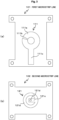
- Fig. 3 is a diagram illustrating an example of a shape of the high-frequency power transmission antennas 111, 121 formed in the microstrip lines 101, 102. As illustrated in Fig. 3 , the two high-frequency power transmission antennas 111, 121 have asymmetric shapes (different shapes).
- the first high-frequency power transmission antenna 111 is an open ring-shaped antenna having a notch 111b in a part thereof. That is, the first high-frequency power transmission antenna 111 includes a ring antenna 111a having an open ring shape and a feeder line 111c connected to the inner conductor 6a of the downstream-side coaxial line 6.
- the ring antenna 111a and the inner conductor 6a of the downstream-side coaxial line 6 are electrically connected.
- the line length of the ring antenna 111a (the length of the line from one end portion forming the notch 111b to the other end portion) does not need to be an odd multiple of 1/2 of the wavelength of a transmission signal.
- the second high-frequency power transmission antenna 121 is a closed ring-shaped antenna without a notch. That is, the second high-frequency power transmission antenna 121 includes a ring antenna 121a having a closed ring shape, a feeder line 121c connected to the inner conductor 5a of the upstream-side coaxial line 5, and a hole 121d forming a part of the through hole 124.
- the central axes of the ring antennas 111a, 121a are disposed on the same line. This makes it possible to strengthen the electromagnetic coupling of the ring antennas 111a, 121a.
- the feeder line 111c of the first high-frequency power transmission antenna 111 is formed to extend from the ring antenna 111a toward the outside of the ring to a position near the outer edge of the first microstrip line 101.
- the feeder line 121c of the second high-frequency power transmission antenna 121 is formed to extend from the ring antenna 121a toward the inside of the ring to the center position of the second microstrip line 102.
- Fig. 4 is a diagram illustrating a configuration example of the DC block 4 and its peripheral members of the present embodiment.
- the first microstrip line 101 is attached to a first insulating jig 105 with a screw
- the second microstrip line 102 is attached to a second insulating jig 106 with a screw. Then, the first insulating jig 105 and the second insulating jig 106 are fixed by screws.
- the terminals 107, 108 are connected to the high-frequency power transmission antennas 111, 121, respectively, and high-frequency power is input and output through the terminals 107, 108.
- the terminal 107 is provided with one pin 107a at the center and four legs 107b at the four corners, and the first microstrip line 101 is sandwiched by the four legs 107b.
- lower two legs 107b are connected to the ground conductor layer 113, and the pin 107a at the center is connected to the feeder line 111c of the first high-frequency power transmission antenna 111.
- the terminal 108 is provided with one pin 108a at the center, and this is connected to the feeder line 121c of the second high-frequency power transmission antenna 121 by being inserted into the through hole 124 from the hole 121d of the second microstrip line 102, and the bottom surface portion around the pin 108a is connected to the ground conductor layer 123.
- the high-frequency power transmission antenna 111, 121 are formed on the two microstrip lines 101, 102, respectively, to realize transmission of high-frequency power, it is possible to reduce the size of the DC block 4 as compared with a conventional DC block using a coaxial line shape or a waveguide shape. In addition, it is possible to highly efficiently transmit only the high-frequency power while cutting off the high-voltage direct-current power by the insulating sheet 103 sandwiched between the high-frequency power transmission antennas 111, 121, which are asymmetric.
- the reduced-size DC block 4 compatible with a combination of high-frequency low power and high-voltage direct-current power.
- the ring width, the ring diameter, the notch position, the notch width, the number of notches of each of the ring antennas 111a, 121a, and the line width of each of the feeder lines 111c, 121c it is possible to highly efficiently transmit only high-frequency power of a desired frequency while blocking high-voltage direct-current power of several kV class by the insulating sheet 103.
- Fig. 5 is a diagram illustrating a configuration example of a plasma generator according to a first modification.
- the plasma generator according to the first modification is configured to improve plasma acceleration performance by applying a voltage to the plasma generation antenna 11.
- the plasma generator according to the first modification further includes a direct-current power supply 7, and includes a DC block 4' instead of the DC block 4.
- the direct-current power supply 7 is a voltage application circuit for applying a direct-current voltage to the plasma generation antenna 11 connected to the inner conductor 6a of the downstream-side coaxial line 6.
- the DC block 4' is configured to draw a direct-current voltage from the first high-frequency power transmission antenna 111 connected to the inner conductor 6a of the downstream-side coaxial line 6 to the direct-current power supply 7.
- Fig. 6 is a diagram illustrating a configuration example of a first microstrip line 101' according to a first modification.
- the same components as those illustrated in Fig. 3(a) are denoted by the same reference signs.
- a wiring pattern 115 for electrically connecting the first high-frequency power transmission antenna 111 and the direct-current power supply 7 is formed on the first microstrip line 101' according to the first modification.
- the wiring pattern 115 is designed to have a line width and a length that do not affect high-frequency waves to be transmitted.
- the wiring pattern 115 is electrically connected to the ring antenna 111a of the first high-frequency power transmission antenna 111.
- wiring 8a illustrated in Fig. 5 connects the wiring pattern 115 to the direct-current power supply 7.
- the direct-current power supply 7 and the plasma generation antenna 11 of the plasma generation chamber 1 are electrically connected via the wiring 8a, the wiring pattern 115 and the first high-frequency power transmission antenna 111 of the DC block 4', and the inner conductor 6a of the downstream-side coaxial line 6.
- the wall surface 13 of the plasma generation chamber 1 and the direct-current power supply 7 are connected by wiring 8b.
- Non Patent Literature 1 As a configuration for applying a voltage to the plasma generation antenna 11 of the plasma generation chamber 1, conventionally, as described in Non Patent Literature 1, a method in which a T-shaped connector and a stub tuner are disposed on the downstream-side coaxial line 6, only a core wire is taken out, and a voltage is applied has been common. However, the introduction of the T-shaped connector and the stub tuner has been a major obstacle to size reduction.
- the plasma generator can be reduced in size. This is equivalent to size reduction of the plasma generator by including the functions of the T-shaped connector and the stub tuner in the DC block 4'.
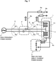
- Fig. 7 is a diagram illustrating a configuration example of a plasma generator according to a second modification.
- the same components as those illustrated in Fig. 5 are denoted by the same reference signs.
- the plasma generator according to the second modification also improves plasma acceleration performance by applying a voltage to the plasma generation antenna 11, and is similar to Fig. 6 in that the wiring pattern 115 is formed on the first microstrip line 101'.
- resistors 9a, 9b connected to a direct-current power supply (main power supply not illustrated) of the plasma generator are provided instead of the direct-current power supply 7 illustrated in Fig. 5 .
- the resistor 9c is also provided on the wiring connecting the high-voltage direct-current power source 3 and the wall surface 13 of the plasma generation chamber 1. Any of the resistors 9a, 9b, and 9c may have a value of 0 Q (no resistance).
- the wiring 8a connected from the first high-frequency power transmission antenna 111 via the wiring pattern 115, and the wiring 8b connected from the wall surface 13 of the plasma generation chamber 1 are connected to the main power supply of the plasma generator via the plurality of resistors 9a, 9b (including 0 ⁇ ).
- resistors 9a, 9b including 0 ⁇ .
- the potential change of the plasma generation antenna 11 and the wall surface 13 of the plasma generation chamber 1 can be realized by resistance connection using the main power supply (plasma electromotive force) of the plasma generator.
- the direct-current power supply 7 it is not necessary to provide the direct-current power supply 7 separately from the main power supply of the plasma generator, and the plasma generator can be reduced in size. That is, by using the resistors 9a, 9b instead of the direct-current power supply 7, it is possible to significantly reduce the size of the plasma generator and simplify the plasma generator.
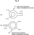
- both of the two high-frequency power transmission antennas may have the closed ring shape, or both of the two high-frequency power transmission antennas 111, 121' may have an open ring shape as illustrated in Fig. 8 .
- At least one of the ring width, the ring diameter, the notch position, the notch width, and the number of notches of each of the two high-frequency power transmission antennas 111, 121' may be configured asymmetrically.
- Forming both of the two high-frequency power transmission antennas 111, 121' in an open ring shape enables strengthening of electromagnetic coupling.
- the ring antennas 111a, 121a' such that the central axes thereof are on the same line and the notches 111b, 121b' are at symmetrical positions (positions shifted by 180 degrees) with respect to the central axes, it is possible to further strengthen the electromagnetic coupling of the ring antennas 111a, 121a'.
Landscapes
- Physics & Mathematics (AREA)
- Electromagnetism (AREA)
- Engineering & Computer Science (AREA)
- Plasma & Fusion (AREA)
- Spectroscopy & Molecular Physics (AREA)
- Plasma Technology (AREA)
- Waveguide Aerials (AREA)
Abstract
Description
- The present invention relates to a DC block that transmits high-frequency power and cuts off direct-current power, and a plasma generator using the DC block.
- Conventionally, a DC block is known as a device for preventing a direct current (DC) from flowing into a high-frequency signal, and is used in various technical fields. As an example, there is an application to spacecraft engines. Some types of spacecraft engines use electricity to discharge propellant, and are called electric propulsion rockets. A typical electric propulsion rocket has a discharge mechanism for ionizing a propellant to generate plasma and an acceleration mechanism for accelerating the plasma.
- Here, it is necessary to send high-frequency power used in high-frequency discharge when plasma is generated, and high-voltage direct-current power necessary for acceleration of the generated plasma, to a plasma generation chamber which is a container for generating plasma. The device that interrupts the interference between the high-frequency power and the direct-current power is a DC block, is disposed on a transmission line of the high-frequency power, and transmits only the high-frequency power and interrupts the direct-current power. That is, a DC block is used as a device that separates high-frequency power for plasma generation and high-voltage direct-current power for plasma acceleration.
- In addition, it is known that acceleration performance of plasma can be improved by applying a direct-current voltage to a plurality of wall surfaces in contact with plasma inside the plasma generation chamber (see, for example, Non Patent Literature 1).
Non Patent Literature 1 discloses that particularly remarkable performance improvement is caused by applying a voltage to an antenna for oscillating high-frequency power inside a plasma generation chamber. As a method of applying a voltage to an antenna, a method is disclosed in which a T-shaped portion is provided in a microwave transmission path, only a core wire is taken out, and the voltage is applied. - Note that a high-frequency signal device is known in which two open ring-shaped resonators formed on different planes are disposed to face each other to enable direct-current power or a low-frequency signal to be transmitted, and the resonators are electromagnetically coupled to each other to enable a high-frequency signal to be transmitted (see, for example, Patent Literature 1).
Patent Literature 1 also discloses that two resonators are disposed to face each other with a spacer plate made of an insulator interposed therebetween. - Patent Literature 1:
JP 2009-246810 A
Non Patent Literature 1: "An experimental evaluation of an influence on mass utilization efficiency by changing a static magnetic field and electric potentials inside 1W-class water ion thruster" (Yasuho ATAKA, Yuichi NAKAGAWA, Hiroyuki KOIZUMI, Kimiya KOMURASAKI; Proceedings of the 50th JSASS Annual Meeting; April 18 and 19, 2019) - The DC block is often required for use of high-frequency power in technical fields on the ground other than spacecraft engines, but the application thereof is often limited to a combination of high-frequency low power (1 to 100 W) and a direct-current low voltage (1 to 100 V) or a combination of high-frequency high power (100 to 10000 W) and a direct-current high voltage (1 to 10 kV). In general, the latter DC block is a large device.
- On the other hand, in a DC block used for an electric propulsion rocket that is space equipment, a combination of high-frequency low power (1 to 100 W) and a direct-current high voltage (1 to 10 kV) is required, and significant size reduction is required. In particular, in the case of application to a small spacecraft engine, significant size reduction is required. However, such high-frequency low power and a direct-current high voltage and ultra-small size has not been realized in a conventional DC block configured using a coaxial line shape or a waveguide shape.
- In the case of a coaxial type DC block, the electrical coupling upstream and downstream of the coaxial line is capacitive. Therefore, it is necessary to overlap an outer conductor of an upstream-side coaxial line and an outer conductor of a downstream-side coaxial line with an insulator interposed therebetween, and also to overlap an upstream-side inner conductor and a downstream-side inner conductor with an insulator interposed therebetween. Furthermore, in order to efficiently transmit microwaves (electromagnetic waves), it is also necessary to adjust impedance to a predetermined value by designing the inner diameter of each conductor and the outer diameter of each conductor to have a predetermined ratio. In order to increase the withstand voltage under these restrictions, it is necessary to stack layers in a radial direction such as inner conductor upstream - insulation - inner conductor downstream - dielectric - outer conductor downstream - insulation - outer conductor upstream, and it is inevitable to increase the size of the device as the voltage increases.
- On the other hand, in the case of a waveguide type DC block, since the electrical coupling is based on electromagnetic waves, it is not necessary to stack the layers as in the case of the coaxial type. Therefore, it can be said that insulation can be achieved by sandwiching one insulating sheet (or insulating plate) between the upstream and downstream waveguides, and it is suitable for a high withstand voltage. However, the minimum size of the waveguide is determined on the principle of passing microwaves inside. For example, when a microwave of 4 to 5 GHz is passed, the minimum size is 48 mm × 22 mm. Therefore, there is a clear lower limit to size reduction.
- The present invention has been made to solve such a problem, and an object of the present invention is to provide a reduced-size DC block compatible with a combination of high-frequency low power and a direct-current high voltage.
- In order to solve the above problem, a DC block of the present invention has a configuration in which two high-frequency power transmission antennas formed on two microstrip lines, respectively, are disposed to face each other with an insulating sheet interposed between the two high-frequency power transmission antennas.
- According to the present invention configured as described above, since the transmission of the high-frequency power is realized by forming the high-frequency power transmission antennas on the microstrip lines, it is not necessary to stack the layers as in the case of the coaxial type in order to increase the withstand voltage, and the minimum size is not limited on the principle of passing the microwaves as in the case of the waveguide type, and the size of the DC block can be reduced as compared with the conventional DC block using the coaxial line shape or the waveguide shape. In addition, it is possible to highly efficiently transmit only the high-frequency power while cutting off the high-voltage direct-current power by the insulating sheet sandwiched between the two high-frequency power transmission antennas. As a result, it is possible to provide the reduced-size DC block compatible with a combination of high-frequency low power and a direct-current high voltage.
-
-
Fig. 1 is a diagram illustrating a configuration example of a plasma generator to which a DC block according to the present embodiment is applied. -
Fig. 2 is a diagram illustrating a configuration example of the DC block according to the present embodiment. -
Fig. 3 is a diagram illustrating an example of a shape of a high-frequency power transmission antenna according to the present embodiment. -
Fig. 4 is a diagram illustrating a configuration example of the DC block and its peripheral members of the present embodiment. -
Fig. 5 is a diagram illustrating a configuration example of a plasma generator according to a first modification. -
Fig. 6 is a diagram illustrating a configuration example of a first microstrip line according to the first modification. -
Fig. 7 is a diagram illustrating a configuration example of a plasma generator according to a second modification. -
Fig. 8 is a diagram illustrating another example of a shape of the high-frequency power transmission antenna according to the present embodiment. - Hereinafter, an embodiment of the present invention will be described with reference to the drawings.
Fig. 1 is a diagram illustrating a configuration example of a plasma generator to which a DC block according to the present embodiment is applied. As illustrated inFig. 1 , the plasma generator according to the present embodiment includes aplasma generation chamber 1, a high-frequency power source 2, a high-voltage direct-current power source 3, and aDC block 4. - The
plasma generation chamber 1 is a container for generating plasma by discharge using high-frequency power and for accelerating the generated plasma by high-voltage direct-current power. Theplasma generation chamber 1 includes aplasma generation antenna 11, a plurality ofmagnets 12 disposed on awall surface 13, and anaccelerator grid 14. In theplasma generation chamber 1, a magnetic field is formed by the plurality ofmagnets 12, and plasma discharge is performed by introducing high-frequency waves such as microwaves from theplasma generation antenna 11. The generated plasma is accelerated by a screen grid for plasma discharge installed on a surface of thewall surface 13 facing the accelerator grid, and theaccelerator grid 14. - The high-
frequency power source 2 supplies high-frequency power for plasma generation to theplasma generation chamber 1. The high-frequency power source 2 and theplasma generation chamber 1 are connected by twocoaxial lines DC block 4. Thecoaxial line 5 on the upstream side includes aninner conductor 5a and anouter conductor 5b, and thecoaxial line 6 on the downstream side includes aninner conductor 6a and anouter conductor 6b. Theinner conductor 6a of the downstream-sidecoaxial line 6 is connected to theplasma generation antenna 11. Theouter conductor 6b of the downstream-sidecoaxial line 6 is connected to themagnets 12 via thewall surface 13 of theplasma generation chamber 1. - The high-voltage direct-
current power source 3 supplies high-voltage direct-current power for plasma generation to theplasma generation chamber 1. The high-voltage direct-current power source 3 is connected to thewall surface 13 of theplasma generation chamber 1 and theaccelerator grid 14. A high voltage exceeding 1 kV is applied between thewall surface 13 and theaccelerator grid 14, and the plasma is accelerated and discharged by the potential difference, and is discharged toward an infinite potential (0 V) of the space. - The
DC block 4 is disposed oncoaxial lines plasma generation chamber 1, and transmits only the high-frequency power and cuts off the direct-current power. The configuration of theDC block 4 will be described in detail with reference toFigs. 2 to 4 . -
Fig. 2 is a diagram illustrating a configuration example of theDC block 4, in whichFig. 2(a) is a perspective view andFig. 2(b) is a side view.Fig. 2(b) is a schematic diagram of the layer structure, and does not accurately illustrate the thickness of each layer. As illustrated inFig. 2 , theDC block 4 of the present embodiment is configured by forming two high-frequencypower transmission antennas microstrip lines power transmission antennas Fig. 2(a) ) interposed therebetween. - As illustrated in
Fig. 2(b) , thefirst microstrip line 101 has a layer structure including a wiring conductor layer in which the first high-frequencypower transmission antenna 111 is formed, aground conductor layer 113 in which the first high-frequencypower transmission antenna 111 is not formed, and adielectric layer 112 sandwiched between the wiring conductor layer and theground conductor layer 113. In the present embodiment, theground conductor layer 113 is formed on one plane of thedielectric layer 112. In addition, the first high-frequencypower transmission antenna 111 is disposed on another plane of thedielectric layer 112, and the first high-frequencypower transmission antenna 111 itself is a wiring conductor layer. InFig. 2(a) , the first high-frequencypower transmission antenna 111 appears not to protrude outward from the surface of thedielectric layer 112, but actually protrudes by the thickness of the first high-frequencypower transmission antenna 111. - The
second microstrip line 102 similarly has a layer structure including a wiring conductor layer in which the second high-frequencypower transmission antenna 121 is formed, aground conductor layer 123 in which the second high-frequencypower transmission antenna 121 is not formed, and adielectric layer 122 sandwiched between the wiring conductor layer and theground conductor layer 123. Theground conductor layer 123 is formed on one plane of thedielectric layer 122 and the second high-frequencypower transmission antenna 121 is disposed on another plane, and the second high-frequencypower transmission antenna 121 itself is a wiring conductor layer. - The two
microstrip lines power transmission antennas 111, 121) face each other with the insulatingsheet 103 interposed therebetween, and the ground conductor layers 113, 123 of the twomicrostrip lines sheet 103. - In the
first microstrip line 101, the first high-frequencypower transmission antenna 111 is connected to theinner conductor 6a of the downstream-sidecoaxial line 6 via a terminal 107 illustrated inFig. 4 , and theground conductor layer 113 is connected to theouter conductor 6b of the downstream-sidecoaxial line 6 via theterminal 107. - In the
second microstrip line 102, a throughhole 124 penetrating the second high-frequencypower transmission antenna 121, thedielectric layer 122, and theground conductor layer 123 is formed. The second high-frequencypower transmission antenna 121 is connected to theinner conductor 5a of the upstream-sidecoaxial line 5 via a terminal 108 inFig. 4 connected to the throughhole 124, and theground conductor layer 123 is connected to theouter conductor 5b of the upstream-sidecoaxial line 5 via theterminal 108. -
Fig. 3 is a diagram illustrating an example of a shape of the high-frequencypower transmission antennas microstrip lines Fig. 3 , the two high-frequencypower transmission antennas - The first high-frequency
power transmission antenna 111 is an open ring-shaped antenna having anotch 111b in a part thereof. That is, the first high-frequencypower transmission antenna 111 includes aring antenna 111a having an open ring shape and afeeder line 111c connected to theinner conductor 6a of the downstream-sidecoaxial line 6. By connecting the terminal 107 illustrated inFig. 4 to thefeeder line 111c and passing wiring from the terminal 107 to theinner conductor 6a of the downstream-sidecoaxial line 6, thering antenna 111a and theinner conductor 6a of the downstream-sidecoaxial line 6 are electrically connected. Note that the line length of thering antenna 111a (the length of the line from one end portion forming thenotch 111b to the other end portion) does not need to be an odd multiple of 1/2 of the wavelength of a transmission signal. - The second high-frequency
power transmission antenna 121 is a closed ring-shaped antenna without a notch. That is, the second high-frequencypower transmission antenna 121 includes aring antenna 121a having a closed ring shape, afeeder line 121c connected to theinner conductor 5a of the upstream-sidecoaxial line 5, and ahole 121d forming a part of the throughhole 124. By connecting the terminal 108 illustrated inFig. 4 to thehole 121d, passing wiring from thefeeder line 121c to theinner conductor 5a of the upstream-sidecoaxial line 5 via the throughhole 124 and the terminal 108, and connecting the wiring to thefeeder line 121c by soldering or the like, thering antenna 121a and theinner conductor 5a of the upstream-sidecoaxial line 5 are electrically connected. - When the first high-frequency
power transmission antenna 111 and the second high-frequencypower transmission antenna 121 are disposed to face each other with the insulatingsheet 103 interposed therebetween, the central axes of thering antennas ring antennas - The
feeder line 111c of the first high-frequencypower transmission antenna 111 is formed to extend from thering antenna 111a toward the outside of the ring to a position near the outer edge of thefirst microstrip line 101. On the other hand, thefeeder line 121c of the second high-frequencypower transmission antenna 121 is formed to extend from thering antenna 121a toward the inside of the ring to the center position of thesecond microstrip line 102. -
Fig. 4 is a diagram illustrating a configuration example of theDC block 4 and its peripheral members of the present embodiment. In theDC block 4 of the present embodiment, thefirst microstrip line 101 is attached to a first insulatingjig 105 with a screw, and thesecond microstrip line 102 is attached to a second insulatingjig 106 with a screw. Then, the first insulatingjig 105 and the second insulatingjig 106 are fixed by screws. - The
terminals power transmission antennas terminals pin 107a at the center and fourlegs 107b at the four corners, and thefirst microstrip line 101 is sandwiched by the fourlegs 107b. At this time, lower twolegs 107b are connected to theground conductor layer 113, and thepin 107a at the center is connected to thefeeder line 111c of the first high-frequencypower transmission antenna 111. In addition, the terminal 108 is provided with onepin 108a at the center, and this is connected to thefeeder line 121c of the second high-frequencypower transmission antenna 121 by being inserted into the throughhole 124 from thehole 121d of thesecond microstrip line 102, and the bottom surface portion around thepin 108a is connected to theground conductor layer 123. - As described above, in the
DC block 4 of the present embodiment, since the high-frequencypower transmission antenna microstrip lines DC block 4 as compared with a conventional DC block using a coaxial line shape or a waveguide shape. In addition, it is possible to highly efficiently transmit only the high-frequency power while cutting off the high-voltage direct-current power by the insulatingsheet 103 sandwiched between the high-frequencypower transmission antennas - As a result, it is possible to provide the reduced-
size DC block 4 compatible with a combination of high-frequency low power and high-voltage direct-current power. Here, by appropriately designing at least one of the ring width, the ring diameter, the notch position, the notch width, the number of notches of each of thering antennas feeder lines sheet 103. -
Fig. 5 is a diagram illustrating a configuration example of a plasma generator according to a first modification. InFig. 5 , the same components as those illustrated inFig. 1 are denoted by the same reference signs. The plasma generator according to the first modification is configured to improve plasma acceleration performance by applying a voltage to theplasma generation antenna 11. - As illustrated in
Fig. 5 , the plasma generator according to the first modification further includes a direct-current power supply 7, and includes a DC block 4' instead of theDC block 4. The direct-current power supply 7 is a voltage application circuit for applying a direct-current voltage to theplasma generation antenna 11 connected to theinner conductor 6a of the downstream-sidecoaxial line 6. The DC block 4' is configured to draw a direct-current voltage from the first high-frequencypower transmission antenna 111 connected to theinner conductor 6a of the downstream-sidecoaxial line 6 to the direct-current power supply 7. -
Fig. 6 is a diagram illustrating a configuration example of a first microstrip line 101' according to a first modification. InFig. 6 , the same components as those illustrated inFig. 3(a) are denoted by the same reference signs. As illustrated inFig. 6 , on the first microstrip line 101' according to the first modification, awiring pattern 115 for electrically connecting the first high-frequencypower transmission antenna 111 and the direct-current power supply 7 is formed. Thewiring pattern 115 is designed to have a line width and a length that do not affect high-frequency waves to be transmitted. - The
wiring pattern 115 is electrically connected to thering antenna 111a of the first high-frequencypower transmission antenna 111. In addition,wiring 8a illustrated inFig. 5 connects thewiring pattern 115 to the direct-current power supply 7. As a result, the direct-current power supply 7 and theplasma generation antenna 11 of theplasma generation chamber 1 are electrically connected via thewiring 8a, thewiring pattern 115 and the first high-frequencypower transmission antenna 111 of the DC block 4', and theinner conductor 6a of the downstream-sidecoaxial line 6. In addition, thewall surface 13 of theplasma generation chamber 1 and the direct-current power supply 7 are connected by wiring 8b. - As a configuration for applying a voltage to the
plasma generation antenna 11 of theplasma generation chamber 1, conventionally, as described inNon Patent Literature 1, a method in which a T-shaped connector and a stub tuner are disposed on the downstream-sidecoaxial line 6, only a core wire is taken out, and a voltage is applied has been common. However, the introduction of the T-shaped connector and the stub tuner has been a major obstacle to size reduction. - On the other hand, in the first modification, by using the
wiring pattern 115 of thefirst microstrip line 101 and extracting a direct-current voltage from the first high-frequencypower transmission antenna 111 without affecting the transmission of the high-frequency power, the application of the direct-current voltage to theplasma generation antenna 11 is realized without using the T-shaped connector and the stub tuner. Accordingly, the plasma generator can be reduced in size. This is equivalent to size reduction of the plasma generator by including the functions of the T-shaped connector and the stub tuner in the DC block 4'. -
Fig. 7 is a diagram illustrating a configuration example of a plasma generator according to a second modification. InFig. 7 , the same components as those illustrated inFig. 5 are denoted by the same reference signs. Similarly to the first modification, the plasma generator according to the second modification also improves plasma acceleration performance by applying a voltage to theplasma generation antenna 11, and is similar toFig. 6 in that thewiring pattern 115 is formed on the first microstrip line 101'. - In the second modification, as a voltage application circuit for applying a direct-current voltage to the
plasma generation antenna 11 connected to theinner conductor 6a of the downstream-sidecoaxial line 6,resistors current power supply 7 illustrated inFig. 5 . In the example illustrated inFig. 7 , theresistor 9c is also provided on the wiring connecting the high-voltage direct-current power source 3 and thewall surface 13 of theplasma generation chamber 1. Any of theresistors - As described above, in the second modification, the
wiring 8a connected from the first high-frequencypower transmission antenna 111 via thewiring pattern 115, and thewiring 8b connected from thewall surface 13 of theplasma generation chamber 1 are connected to the main power supply of the plasma generator via the plurality ofresistors plasma generation antenna 11 and thewall surface 13 of theplasma generation chamber 1 using the voltage drop in theresistors current power supply 7 of a system different from the main power supply of the plasma generator as illustrated inFig. 5 . - As a result, according to the second modification, the potential change of the
plasma generation antenna 11 and thewall surface 13 of theplasma generation chamber 1 can be realized by resistance connection using the main power supply (plasma electromotive force) of the plasma generator. As a result, it is not necessary to provide the direct-current power supply 7 separately from the main power supply of the plasma generator, and the plasma generator can be reduced in size. That is, by using theresistors current power supply 7, it is possible to significantly reduce the size of the plasma generator and simplify the plasma generator. - In the above embodiment, the example in which only the first high-frequency
power transmission antenna 111 has an open ring shape has been described. However, both of the two high-frequency power transmission antennas may have the closed ring shape, or both of the two high-frequencypower transmission antennas 111, 121' may have an open ring shape as illustrated inFig. 8 . At least one of the ring width, the ring diameter, the notch position, the notch width, and the number of notches of each of the two high-frequencypower transmission antennas 111, 121' may be configured asymmetrically. - Forming both of the two high-frequency
power transmission antennas 111, 121' in an open ring shape enables strengthening of electromagnetic coupling. At this time, by disposing thering antennas notches ring antennas - In addition, each of the above embodiments is merely an example of implementation in implementing the present invention, and the technical scope of the present invention should not be interpreted in a limited manner. That is, the present invention can be implemented in various forms without departing from the gist or main features thereof.
-
- 1 Plasma generation chamber
- 2 High-frequency power source
- 3 High-voltage direct-
current power source 4, 4' DC block - 5, 6 Coaxial line
- 7 Direct-current power supply
- 8a, 8b Wiring
- 9a, 9b, 9c Resistor
- 11 Plasma generation antenna
- 12 Magnet
- 13 Wall surface
- 14 Accelerator grid
- 101, 102 Microstrip line
- 103 Insulating sheet
- 111, 121 High-frequency power transmission antenna (wiring conductor layer)
- 112, 122 Dielectric layer
- 113, 123 Ground conductor layer
- 114, 124 Through hole
- 115 Wiring pattern
Claims (8)
- A DC block wherein two high-frequency power transmission antennas formed on two microstrip lines, respectively, are disposed to face each other with an insulating sheet interposed between the two high-frequency power transmission antennas.
- The DC block according to claim 1, whereineach of the microstrip lines has a layer structure including a wiring conductor layer in which the high-frequency power transmission antennas is formed, a ground conductor layer in which the high-frequency power transmission antenna is not formed, and a dielectric layer sandwiched between the wiring conductor layer and the ground conductor layer, andthe two microstrip lines are disposed to face each other such that the wiring conductor layers of the two microstrip lines face each other with the insulating sheet interposed between the wiring conductor layers, and the ground conductor layers of the two microstrip lines are separated from the insulating sheet.
- The DC block according to claim 1 or 2, whereinat least one of the two high-frequency power transmission antennas has an open ring shape having a notch in a part thereof, andthe two high-frequency power transmission antennas have asymmetric shapes.
- The DC block according to claim 3, whereinboth of the two high-frequency power transmission antennas have open ring shapes each having a notch in a part thereof, andat least one of a ring width, a ring diameter, a notch position, a notch width, and a number of notches of the open ring of each of the two high-frequency power transmission antennas, is asymmetric.
- The DC block according to any one of claims 1 to 4, whereineach of the high-frequency power transmission antennas includes a feeder line connected to an inner conductor of a coaxial line that transmits high-frequency power, andon one of the microstrip lines, a wiring pattern configured to electrically connect the high-frequency power transmission antenna and a voltage application circuit configured to apply a direct-current voltage to the plasma generation antenna connected to the inner conductor of the coaxial line is formed.
- A plasma generator comprising:a plasma generation chamber that is a container configured to generate plasma by discharge using high-frequency power and accelerate the generated plasma by high-voltage direct-current power;a DC block disposed on a transmission line configured to transmit the high-frequency power to the plasma generation chamber, the DC block transmitting only the high-frequency power and cutting off direct-current power, whereinthe DC block has the configuration according to any one of claims 1 to 5.
- The plasma generator according to claim 6, whereinthe DC block has the configuration according to claim 5, andthe plasma generator further comprises a direct-current power supply as the voltage application circuit.
- The plasma generator according to claim 6, whereinthe DC block has the configuration according to claim 5, andthe plasma generator further comprises, as the voltage application circuit, a resistor connected to a direct-current power supply of the plasma generator.
Applications Claiming Priority (1)
| Application Number | Priority Date | Filing Date | Title |
|---|---|---|---|
| PCT/JP2021/010520 WO2022195700A1 (en) | 2021-03-16 | 2021-03-16 | Dc block and plasma generation device using same |
Publications (2)
| Publication Number | Publication Date |
|---|---|
| EP4311022A1 true EP4311022A1 (en) | 2024-01-24 |
| EP4311022A4 EP4311022A4 (en) | 2025-01-15 |
Family
ID=83320103
Family Applications (1)
| Application Number | Title | Priority Date | Filing Date |
|---|---|---|---|
| EP21931452.3A Pending EP4311022A4 (en) | 2021-03-16 | 2021-03-16 | DC BLOCK AND PLASMA GENERATION DEVICE THEREOF |
Country Status (5)
| Country | Link |
|---|---|
| US (1) | US12489184B2 (en) |
| EP (1) | EP4311022A4 (en) |
| JP (1) | JP7464897B2 (en) |
| KR (1) | KR102961567B1 (en) |
| WO (1) | WO2022195700A1 (en) |
Family Cites Families (7)
| Publication number | Priority date | Publication date | Assignee | Title |
|---|---|---|---|---|
| JPS6359101A (en) | 1986-08-28 | 1988-03-15 | Matsushita Electric Ind Co Ltd | Microwave circuit connection device |
| JP3307214B2 (en) * | 1996-02-23 | 2002-07-24 | 三菱電機株式会社 | High frequency coupling line |
| US6930639B2 (en) * | 2002-03-15 | 2005-08-16 | The Board Of Trustees Of The Leland Stanford Junior University | Dual-element microstrip patch antenna for mitigating radio frequency interference |
| EP1543580A1 (en) | 2002-09-27 | 2005-06-22 | Nokia Corporation | Coupling device |
| JP5119514B2 (en) | 2008-01-09 | 2013-01-16 | 独立行政法人 宇宙航空研究開発機構 | Ion injection device, propulsion device, and artificial satellite |
| JP4915747B2 (en) | 2008-03-31 | 2012-04-11 | 国立大学法人徳島大学 | High frequency signal transmission device |
| KR101070633B1 (en) | 2009-10-15 | 2011-10-07 | 주식회사 에이스테크놀로지 | DC Blocking Device Using Impedance Matching |
-
2021
- 2021-03-16 US US18/550,333 patent/US12489184B2/en active Active
- 2021-03-16 WO PCT/JP2021/010520 patent/WO2022195700A1/en not_active Ceased
- 2021-03-16 EP EP21931452.3A patent/EP4311022A4/en active Pending
- 2021-03-16 JP JP2023506423A patent/JP7464897B2/en active Active
- 2021-03-16 KR KR1020237032718A patent/KR102961567B1/en active Active
Also Published As
| Publication number | Publication date |
|---|---|
| EP4311022A4 (en) | 2025-01-15 |
| US12489184B2 (en) | 2025-12-02 |
| JPWO2022195700A1 (en) | 2022-09-22 |
| KR102961567B1 (en) | 2026-05-07 |
| US20240195037A1 (en) | 2024-06-13 |
| WO2022195700A1 (en) | 2022-09-22 |
| JP7464897B2 (en) | 2024-04-10 |
| KR20230149314A (en) | 2023-10-26 |
Similar Documents
| Publication | Publication Date | Title |
|---|---|---|
| US9979067B2 (en) | N-way, ridged waveguide, radial power combiner/divider | |
| EP0711101B1 (en) | A circular accelerator having an ion beam accelerating device | |
| Nicholson | Microwave Rotary Joints for X-, C-, and S-band | |
| Yoneda et al. | A design of novel grooved circular waveguide polarizers | |
| US5703601A (en) | Double layer circularly polarized antenna with single feed | |
| US3786372A (en) | Broadband high frequency balun | |
| EP2812944B1 (en) | Superluminal antenna | |
| EP2281321B1 (en) | Power splitter | |
| JPH04271605A (en) | Feeder device for radiation element operated by two polarizes waves | |
| EP3333968A1 (en) | A directional coupler and a method of manufacturing thereof | |
| Nwajana et al. | Microwave diplexer purely based on direct synchronous and asynchronous coupling | |
| CN113972489B (en) | Antenna and electronic device | |
| Rao et al. | Analysis of the metal plate coupled resonator with its compact in-line filter design applications | |
| US12489184B2 (en) | DC block and plasma generator using the same | |
| JPH11261308A (en) | Triplate line interlayer connector | |
| Bryant | Coaxial transmission lines, related two-conductor transmission lines, connectors, and components: A US historical perspective | |
| US5281932A (en) | Multilayer magnetically coupled suspended stripline for impedance matching | |
| Gupta et al. | A dual-band balun architecture with unequal port-terminations | |
| WO2017083100A2 (en) | Stripline feed structure for superluminal antenna array | |
| US3289110A (en) | Non-reciprocal multi-element tem transmission line device | |
| Yoneda et al. | A 90 GHz-band monoblock type waveguide orthomode transducer | |
| Wu et al. | Microfabrication of coaxial filter without internal conductor support | |
| CN115492736A (en) | Magnetic circuit-free microwave coaxial resonance ion thruster and thrust forming method | |
| US3096474A (en) | Microwave frequency converter | |
| US12244079B1 (en) | Circularly polarized solderless antenna with frequency-scalable circuit |
Legal Events
| Date | Code | Title | Description |
|---|---|---|---|
| STAA | Information on the status of an ep patent application or granted ep patent |
Free format text: STATUS: THE INTERNATIONAL PUBLICATION HAS BEEN MADE |
|
| PUAI | Public reference made under article 153(3) epc to a published international application that has entered the european phase |
Free format text: ORIGINAL CODE: 0009012 |
|
| STAA | Information on the status of an ep patent application or granted ep patent |
Free format text: STATUS: REQUEST FOR EXAMINATION WAS MADE |
|
| 17P | Request for examination filed |
Effective date: 20231014 |
|
| AK | Designated contracting states |
Kind code of ref document: A1 Designated state(s): AL AT BE BG CH CY CZ DE DK EE ES FI FR GB GR HR HU IE IS IT LI LT LU LV MC MK MT NL NO PL PT RO RS SE SI SK SM TR |
|
| DAV | Request for validation of the european patent (deleted) | ||
| DAX | Request for extension of the european patent (deleted) | ||
| REG | Reference to a national code |
Ref country code: DE Ref legal event code: R079 Free format text: PREVIOUS MAIN CLASS: H01P0005020000 Ipc: H05H0001460000 |
|
| A4 | Supplementary search report drawn up and despatched |
Effective date: 20241216 |
|
| RIC1 | Information provided on ipc code assigned before grant |
Ipc: H01Q 13/08 20060101ALI20241210BHEP Ipc: H01P 5/02 20060101ALI20241210BHEP Ipc: H05H 1/46 20060101AFI20241210BHEP |