EP4311020A1 - Solderable waveguide antenna - Google Patents
Solderable waveguide antenna Download PDFInfo
- Publication number
- EP4311020A1 EP4311020A1 EP23163661.4A EP23163661A EP4311020A1 EP 4311020 A1 EP4311020 A1 EP 4311020A1 EP 23163661 A EP23163661 A EP 23163661A EP 4311020 A1 EP4311020 A1 EP 4311020A1
- Authority
- EP
- European Patent Office
- Prior art keywords
- waveguide
- pcb
- metallic portions
- solder
- assembly
- Prior art date
- Legal status (The legal status is an assumption and is not a legal conclusion. Google has not performed a legal analysis and makes no representation as to the accuracy of the status listed.)
- Pending
Links
Images




Classifications
-
- H—ELECTRICITY
- H01—ELECTRIC ELEMENTS
- H01Q—ANTENNAS, i.e. RADIO AERIALS
- H01Q1/00—Details of, or arrangements associated with, antennas
- H01Q1/36—Structural form of radiating elements, e.g. cone, spiral, umbrella; Particular materials used therewith
- H01Q1/38—Structural form of radiating elements, e.g. cone, spiral, umbrella; Particular materials used therewith formed by a conductive layer on an insulating support
-
- H—ELECTRICITY
- H01—ELECTRIC ELEMENTS
- H01Q—ANTENNAS, i.e. RADIO AERIALS
- H01Q13/00—Waveguide horns or mouths; Slot antennas; Leaky-waveguide antennas; Equivalent structures causing radiation along the transmission path of a guided wave
- H01Q13/06—Waveguide mouths
-
- H—ELECTRICITY
- H01—ELECTRIC ELEMENTS
- H01P—WAVEGUIDES; RESONATORS, LINES, OR OTHER DEVICES OF THE WAVEGUIDE TYPE
- H01P3/00—Waveguides; Transmission lines of the waveguide type
- H01P3/12—Hollow waveguides
- H01P3/121—Hollow waveguides integrated in a substrate
-
- H—ELECTRICITY
- H01—ELECTRIC ELEMENTS
- H01P—WAVEGUIDES; RESONATORS, LINES, OR OTHER DEVICES OF THE WAVEGUIDE TYPE
- H01P11/00—Apparatus or processes specially adapted for manufacturing waveguides or resonators, lines, or other devices of the waveguide type
- H01P11/001—Manufacturing waveguides or transmission lines of the waveguide type
- H01P11/003—Manufacturing lines with conductors on a substrate, e.g. strip lines, slot lines
-
- H—ELECTRICITY
- H01—ELECTRIC ELEMENTS
- H01Q—ANTENNAS, i.e. RADIO AERIALS
- H01Q1/00—Details of, or arrangements associated with, antennas
- H01Q1/12—Supports; Mounting means
- H01Q1/22—Supports; Mounting means by structural association with other equipment or articles
- H01Q1/2283—Supports; Mounting means by structural association with other equipment or articles mounted in or on the surface of a semiconductor substrate as a chip-type antenna or integrated with other components into an IC package
-
- H—ELECTRICITY
- H01—ELECTRIC ELEMENTS
- H01Q—ANTENNAS, i.e. RADIO AERIALS
- H01Q1/00—Details of, or arrangements associated with, antennas
- H01Q1/36—Structural form of radiating elements, e.g. cone, spiral, umbrella; Particular materials used therewith
-
- H—ELECTRICITY
- H01—ELECTRIC ELEMENTS
- H01Q—ANTENNAS, i.e. RADIO AERIALS
- H01Q1/00—Details of, or arrangements associated with, antennas
- H01Q1/50—Structural association of antennas with earthing switches, lead-in devices or lightning protectors
-
- H—ELECTRICITY
- H01—ELECTRIC ELEMENTS
- H01Q—ANTENNAS, i.e. RADIO AERIALS
- H01Q1/00—Details of, or arrangements associated with, antennas
- H01Q1/52—Means for reducing coupling between antennas; Means for reducing coupling between an antenna and another structure
- H01Q1/526—Electromagnetic shields
-
- H—ELECTRICITY
- H05—ELECTRIC TECHNIQUES NOT OTHERWISE PROVIDED FOR
- H05K—PRINTED CIRCUITS; CASINGS OR CONSTRUCTIONAL DETAILS OF ELECTRIC APPARATUS; MANUFACTURE OF ASSEMBLAGES OF ELECTRICAL COMPONENTS
- H05K3/00—Apparatus or processes for manufacturing printed circuits
- H05K3/30—Assembling printed circuits with electric components, e.g. with resistors
- H05K3/32—Assembling printed circuits with electric components, e.g. with resistors electrically connecting electric components or wires to printed circuits
- H05K3/34—Assembling printed circuits with electric components, e.g. with resistors electrically connecting electric components or wires to printed circuits by soldering
-
- H—ELECTRICITY
- H10—SEMICONDUCTOR DEVICES; ELECTRIC SOLID-STATE DEVICES NOT OTHERWISE PROVIDED FOR
- H10W—GENERIC PACKAGES, INTERCONNECTIONS, CONNECTORS OR OTHER CONSTRUCTIONAL DETAILS OF DEVICES COVERED BY CLASS H10
- H10W44/00—Electrical arrangements for controlling or matching impedance
- H10W44/20—Electrical arrangements for controlling or matching impedance at high-frequency [HF] or radio frequency [RF]
-
- H—ELECTRICITY
- H05—ELECTRIC TECHNIQUES NOT OTHERWISE PROVIDED FOR
- H05K—PRINTED CIRCUITS; CASINGS OR CONSTRUCTIONAL DETAILS OF ELECTRIC APPARATUS; MANUFACTURE OF ASSEMBLAGES OF ELECTRICAL COMPONENTS
- H05K1/00—Printed circuits
- H05K1/02—Details
- H05K1/0213—Electrical arrangements not otherwise provided for
- H05K1/0237—High frequency adaptations
- H05K1/0243—Printed circuits associated with mounted high frequency components
-
- H—ELECTRICITY
- H05—ELECTRIC TECHNIQUES NOT OTHERWISE PROVIDED FOR
- H05K—PRINTED CIRCUITS; CASINGS OR CONSTRUCTIONAL DETAILS OF ELECTRIC APPARATUS; MANUFACTURE OF ASSEMBLAGES OF ELECTRICAL COMPONENTS
- H05K1/00—Printed circuits
- H05K1/18—Printed circuits structurally associated with non-printed electric components
- H05K1/181—Printed circuits structurally associated with non-printed electric components associated with surface mounted components
-
- H—ELECTRICITY
- H05—ELECTRIC TECHNIQUES NOT OTHERWISE PROVIDED FOR
- H05K—PRINTED CIRCUITS; CASINGS OR CONSTRUCTIONAL DETAILS OF ELECTRIC APPARATUS; MANUFACTURE OF ASSEMBLAGES OF ELECTRICAL COMPONENTS
- H05K2201/00—Indexing scheme relating to printed circuits covered by H05K1/00
- H05K2201/10—Details of components or other objects attached to or integrated in a printed circuit board
- H05K2201/10007—Types of components
- H05K2201/10098—Components for radio transmission, e.g. radio frequency identification [RFID] tag, printed or non-printed antennas
-
- H—ELECTRICITY
- H10—SEMICONDUCTOR DEVICES; ELECTRIC SOLID-STATE DEVICES NOT OTHERWISE PROVIDED FOR
- H10W—GENERIC PACKAGES, INTERCONNECTIONS, CONNECTORS OR OTHER CONSTRUCTIONAL DETAILS OF DEVICES COVERED BY CLASS H10
- H10W44/00—Electrical arrangements for controlling or matching impedance
- H10W44/20—Electrical arrangements for controlling or matching impedance at high-frequency [HF] or radio frequency [RF]
- H10W44/203—Electrical connections
- H10W44/216—Waveguides, e.g. strip lines
Definitions
- Radio frequency (RF) waveguide antennas e.g., waveguides
- PCB printed circuit boards
- Conventional techniques of affixation often rely on screws (or other fasteners) or pressure sensitive adhesives (PSA). While such techniques may affix the waveguides to the PCBs, they often fail to do so in a cost effective and/or precise manner (e.g., with proper alignment and/or with proper standoff heights of one or more apertures relative to the PCBs).
- the RF waveguide has a plastic body with a waveguide channel that has an aperture configured to mate with a corresponding RF port of a PCB.
- the RF waveguide also has a plurality of dimples on one or more external surfaces of the plastic body and one or more waveguide metallic portions disposed on the dimples.
- an assembly that includes a PCB with an RF port and one or more PCB metallic portions.
- the assembly also includes a waveguide that has a waveguide channel with an aperture aligned with the RF port of the PCB and one or more waveguide metallic portions disposed on one or more external surfaces of the waveguide.
- the waveguide metallic portions correspond to the PCB metallic portions.
- the assembly further includes solder disposed between the waveguide metallic portions and the PCB metallic portions.
- the method includes obtaining a plastic waveguide comprising a plurality of dimples and depositing solderable metal on the dimples to form one or more waveguide metallic portions.
- the method also includes obtaining a PCB comprising one or more PCB metallic portions and adhering solder balls to the waveguide metallic portions and/or the PCB metallic portions.
- the method further includes arranging the plastic waveguide proximate the PCB such that the solder balls are in contact with the waveguide metallic portions and the PCB metallic portions and applying heat to the PCB or the plastic waveguide effective to melt the solder balls and affix the plastic waveguide to the PCB.
- RF waveguide antennas e.g., waveguides
- PCBs for various reasons (e.g., packaging, signal preservation, cost).
- Conventional techniques of affixation often rely on screws (or other fasteners) or pressure sensitive adhesives (PSA). While such techniques may affix the waveguides to the PCBs, they often fail to do so in a cost effective and/or precise manner (e.g., alignment and/or standoff heights of one or more apertures relative to the PCBs).
- a waveguide that is configured to be soldered to a PCB via one or more metallic portions disposed thereon. Additionally, the waveguide may have solder disposed within thru holes that is configured to conduct heat from one or more components of the PCB, such as a Monolithic Microwave Integrated Circuit (MN ⁇ C), when the waveguide is mounted to the PCB. Also described herein is an assembly comprising the waveguide soldered to the PCB via solder between the metallic portions of the waveguide and metallic portions of the PCB. Techniques for producing the waveguide and the assembly are also described herein. For example, the metallic portions of the waveguide may be deposited onto a plastic body of the waveguide and such that the metallic portions may be soldered to corresponding metallic portions on the PCB.
- MN ⁇ C Monolithic Microwave Integrated Circuit
- soldering the waveguide to the PCB By soldering the waveguide to the PCB, a cheap, precise, and secure mechanical bonding may be achieved while electrically sealing features of the waveguide (e.g., an aperture) and/or components of the PCB (e.g., a waveguide port, a MMIC).
- electrically sealing features of the waveguide e.g., an aperture
- components of the PCB e.g., a waveguide port, a MMIC.
- ball grid arrays e.g., solder balls
- solder within the thru holes allows for better heat conduction through the waveguide than traditional waveguides.
- Fig. 1 illustrates an example environment 100 where a solderable waveguide antenna may be implemented.
- the example environment 100 contains a vehicle 102.
- the vehicle 102 may be any vehicle type (taxi, car, truck, motorcycle, e-bike, boat, air vehicle, and so on).
- the vehicle 102 contains an RF assembly 104 comprising a PCB 106 and a waveguide antenna 108 attached thereto.
- the RF assembly 104 may be configured for any type of RF communication (e.g., V2X, 5G, radar).
- the RF assembly 104 may be configured as a radar assembly where the waveguide antenna 108 is configured for transmission and/or reception of radar signals.
- the waveguide antenna 108 may be configured as an air waveguide antenna, a dielectric filled waveguide, have multiple antennas and/or channels, or otherwise be configured as any other waveguide known to those in the art.
- the PCB 106 may be a bare circuit board or have one or more components attached thereto (e.g., a MMIC) prior to assembly with the waveguide antenna 108
- the RF assembly 104 may be configured for other environments.
- the RF assembly 104 may be configured for a residential environment, commercial environment, mobile or stationary environment, marine environment, and/or space environment.
- Fig. 2 illustrates a cross section of the RF assembly 104.
- the RF assembly 104 has the PCB 106 and the waveguide antenna 108.
- the RF assembly 104 also has an enclosure 200 and a radome 202.
- the waveguide antenna 108 is at least partially formed of a plastic material with one or more metallic portions disposed thereon, as discussed further in regard to Fig. 3 .
- the PCB 106 also has metallic portions that correspond to the metallic portions of the waveguide antenna 108, such that the waveguide antenna 108 can be attached to the PCB 106 via solder 204 between the corresponding metallic portions.
- the solder 204 may be any type of solder. In order to not melt the plastic material of the waveguide antenna 108, the solder 204 may be a low melting point solder, such as Sn/Bi or In/Sn.
- solder 204 is illustrated as circular cross sections between the waveguide antenna 108 and the PCB 106, the solder 204 may take any shape after the solder has been reflowed (e.g., melted) to create the RF assembly 104.
- the solder 204 may start as solder balls (e.g., a ball grid array on the waveguide antenna 108 and/or the PCB 106) and flow under heat to produce the RF assembly 104, such that the solder 204 forms one or more contiguous portions.
- the contiguous portions may surround (or at least partially surround) an aperture 206 of a waveguide channel 208 of the waveguide antenna 108, such that the aperture 206 and/or a corresponding RF port 210 of the PCB 106 may be electrically sealed, for example, protected or shielded from Electro Magnetic Interference (EMI).
- EMI Electro Magnetic Interference
- a monolithic microwave integrated circuit (MMIC) 212 is attached to the PCB 106 via solder 214.
- the solder 214 may be a different solder than that of solder 204.
- the solder 214 may be a higher temperature solder because the MMIC 212 may not have the same thermal restrictions as the plastic material of the waveguide antenna 108.
- the MMIC 212 may be mounted/soldered to the PCB 106 prior to the waveguide antenna 108 being attached to the PCB 106.
- a thermal interface material (TIM) 216 Opposite the solder 214 on the MMIC 212 is a thermal interface material (TIM) 216.
- TIM thermal interface material
- the solder 218 may contact the TIM 216 and provide a path for heat conduction between the TIM 216 and an external surface 220 of the waveguide antenna 108.
- the cavities in which the solder 218 is disposed may be considered as thermal vias through the waveguide antenna 108 (e.g., thru holes). In this way, the RF assembly 104 may provide better cooling of the MMIC 212 than the use of a waveguide antenna that does not have the solder 218.
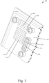
- Fig. 3 illustrates the waveguide antenna 108 with some of the solder 204 and the solder 218 disposed thereon.
- Fig. 3 illustrates the waveguide antenna 108 as it may be configured for attachment to the PCB 106.
- the waveguide antenna 108 has a plurality of apertures 206 in multiple locations. It should be noted that any configuration of apertures 206 (including height from a surface of the waveguide antenna 108) may be used without departing from the scope of this disclosure.
- the solder 204 Surrounding some of the apertures 206 is the solder 204.
- the solder 204 may be disposed in an array around and in between the apertures 206.
- the solder 204 may be attached to waveguide metallic portions 300 disposed on a plastic body 302 of the waveguide antenna 108.
- the waveguide metallic portions 300 (e.g., depositions of the solderable metal) may cover dimples of the plastic body 302 underneath the solder 204 (e.g., a dimple for each solder ball of the solder 204).
- the dimples may be in-molded dimples (e.g., part of the plastic body 302) which enable the solder 204 to stay in a specific location.
- the solder 204 at least partially surrounds the apertures 206 in order to provide shielding after assembly with the PCB 106.
- solder 204 may be disposed on both waveguide metallic portions 300 in the illustrated example; however, some of the solder 204 is not shown (e.g., in the upper waveguide metallic portion 300) to better illustrate the corresponding waveguide metallic portion 300 and the surface to which it is disposed.
- a surface 304 and the solder 218 disposed therethrough are illustrated (e.g., within thermal vias).
- the surface 304 is configured to be proximate the MMIC 212, such that the solder 218 can contact the TIM 216.
- the surface 304 may be flush, raised (as illustrated), or tilted relative to an adjacent surface depending upon the configuration of the MMIC 212 or any other component that can benefit from the heat transfer provided by the solder 218.
- the surface 304 may also be within a cutout or recess formed by the apertures 206 and/or other portions of the plastic body 302 (e.g., for packaging) such that the MMIC 212 may be surrounded (e.g., on a plurality of sides) by the waveguide antenna 108 when the waveguide antenna 108 is assembled to the PCB 106.
- the MMIC 212 (or any other component of the PCB 106) may be at least partially encapsulated by the waveguide antenna 108 when assembled.
- the waveguide antenna 108 may have any number and/or configuration of surfaces 304 for respective components.
- the surface 304 may have a waveguide metallic portion 300 disposed thereon or not.
- a waveguide metallic portion 300 on the surface 304 may enable better heat transfer between portions of the solder 218.
- Fig. 4 is an example method 400 of manufacturing a solderable waveguide antenna.
- a waveguide comprising a plastic body with one or more surfaces configured to mate with corresponding surfaces of a PCB is obtained.
- the plastic body 302 of the waveguide antenna 108 may be obtained with surfaces corresponding to the waveguide metallic portions 300 (but without the waveguide metallic portions 300 disposed thereon).
- a solderable metal is deposited onto the surfaces to create respective metallic portions.
- the metallic portions are solderable features for the solder 204.
- a conductive and/or solderable metal e.g., copper, tin, silver, or an alloy thereof
- PVD Physical Vapor Deposition
- a blocking screen may be used such that locations of the waveguide metallic portions 300 may be controlled (e.g., only around apertures 206, around the surface 304 to electrically seal/shield the MMIC 212, in other locations for structure mounting to the PCB 106).
- the waveguide metallic portions 300 may cover dimples of the plastic body 302 used to house/locate solder.
- solder is deposited onto the metallic portions.
- the solder 204 may be deposited on the waveguide metallic portions 300 within the dimples (e.g., metallurgically bonded).
- the solder 204 may form a ball grid array and be deposited/adhered to the waveguide metallic portions 300 via various known processes.
- the solder 204 may be deposited as 0.2 to 0.5 mm balls and placed at a pitch (e.g., distance from each other).
- the solder 204 may be deposited to the PCB 106, either alternatively or in conjunction, or as part of the assembly process.
- solder may also be deposited within thermal vias of the plastic body (if the waveguide is configured with such).
- the solder 218 may be deposited within the thru holes of the plastic body 302 (e.g., proximate the TIM 216, proximate the MMIC 212).
- Fig. 5 is an example method 500 of attaching a solderable waveguide antenna to a PCB.
- a waveguide comprising one or more waveguide metallic portions and a PCB comprising PCB metallic portions that correspond to the waveguide metallic portions are obtained.
- the waveguide antenna 108 (with the waveguide metallic portions 300) and the PCB 106 (with its metallic portions) may be obtained.
- solder balls are deposited on at least one of the waveguide metallic portions or the PCB metallic portions.
- the solder balls may already be disposed on one or both of the waveguide metallic portions or the PCB metallic portions (e.g., as part of manufacturing the respective parts), thereby obviating step 504.
- the solder 204 may be deposited on the waveguide metallic portions 300 or the PCB metallic portions of the PCB 106.
- the waveguide is arranged proximate the PCB such that the solder balls are in contact with the waveguide metallic portions and the PCB metallic portions.
- the waveguide antenna 108 may be arranged proximate the PCB 106 such that the apertures 206 are aligned with respective RF ports 210.
- the locations of the waveguide metallic portions 300 and the corresponding PCB metallic portions align when the apertures 206 and RF ports 210 are aligned with each other (e.g., due to locations of the respective metallic portions relative to the apertures 206 and RF ports 210).
- heat is applied to the PCB or the waveguide which causes the solder balls to melt, thereby affixing the waveguide to the PCB.
- the arrangement of the PCB and the waveguide may be maintained, such that proper alignment (e.g., aperture to RF port standoff and alignment) is maintained.
- heat may be applied to the PCB 106 or the waveguide antenna 108 effective to melt the solder 204.
- the heat may be a low temp reflow heat, such as 160°C.
- the alignment of the apertures 206 to their respective RF ports 210 may be maintained during the heating process.
- heat is applied to the waveguide effective to melt solder within one or more thermal vias.
- Step 510 may be performed if the waveguide contains the thermal vias.
- heat may be applied to the waveguide antenna 108 effective to melt the solder 218 into the thermal vias of the surface 304 such that the solder 218 is thermally connected to an underlying component (e.g., the MMIC 212 via the TIM 216).
- the solder 218 may then provide a heat transfer path from the underlying component to an external surface (e.g., the external surface 220).
- Example 1 An assembly comprising: a printed circuit board (PCB) comprising: a radio frequency (RF) port; and one or more PCB metallic portions; a waveguide comprising a waveguide channel with an aperture aligned with the RF port of the PCB; and one or more waveguide metallic portions disposed on one or more external surfaces of the waveguide, the waveguide metallic portions corresponding to the PCB metallic portions; and solder disposed between the waveguide metallic portions and the PCB metallic portions.
- PCB printed circuit board
- RF radio frequency
- Example 2 The assembly of example 1, wherein the solder at least partially surrounds the RF port.
- Example 3 The assembly of example 2, wherein the solder is configured to provide electromagnetic interference (EMI) shielding for the RF port.
- EMI electromagnetic interference
- Example 4 The assembly of example 1, wherein: the waveguide is formed of a plastic material; and the waveguide metallic portions are a solderable metal disposed on the plastic material of the external surfaces.
- Example 5 The assembly of example 4, wherein the solderable metal comprises copper, tin, silver, or an alloy thereof.
- Example 6 The assembly of example 4, wherein the waveguide metallic portions comprise depositions of the solderable metal on the plastic material.
- Example 7 The assembly of example 6, wherein the depositions of the solderable metal comprise physical vapor depositions (PVD).
- PVD physical vapor depositions
- Example 8 The assembly of example 1, wherein: the waveguide comprises dimples on the external surfaces; and the waveguide metallic portions and the solder are disposed within the dimples.
- Example 9 The assembly of example 1, wherein: the PCB comprises a monolithic microwave integrated circuit (MN ⁇ C); and the waveguide comprises: a cutout configured to surround the MN ⁇ C; and thru holes disposed within the cutout.
- MN ⁇ C monolithic microwave integrated circuit
- Example 10 The assembly of example 9, further comprising a radome disposed opposite the cutout.
- Example 11 The assembly of example 9, further comprising solder disposed within the thru holes and thermally connected to a thermal interface material (TIM) of the MN ⁇ C.
- TIM thermal interface material
- Example 12 The assembly of example 9, wherein the solder is configured to provide electromagnetic (EMI) shielding for the MN ⁇ C.
- EMI electromagnetic
- Example 13 The assembly of example 1, wherein the solder comprises a tin/bismuth, indium/tin, or other low melting point solder.
- Example 14 A radio frequency (RF) waveguide comprising: a plastic body comprising: a waveguide channel with an aperture configured to mate with a corresponding RF port of a printed circuit board (PCB); and a plurality of dimples on one or more external surfaces of the plastic body; and one or more waveguide metallic portions disposed on the dimples.
- RF radio frequency
- Example 15 A method comprising: obtaining a plastic waveguide comprising a plurality of dimples; depositing solderable metal on the dimples to form one or more waveguide metallic portions; obtaining a printed circuit board (PCB) comprising one or more PCB metallic portions; at least one of: adhering solder balls to the waveguide metallic portions proximate the dimples; or adhering solder balls to the PCB metallic portions; arranging the plastic waveguide proximate the PCB such that the solder balls are in contact with the waveguide metallic portions and the PCB metallic portions; and applying heat to the PCB or the plastic waveguide effective to melt the solder balls and affix the plastic waveguide to the PCB.
- PCB printed circuit board
- Example 16 The method of example 15, wherein depositing the solderable metal on the dimples comprises a physical vapor deposition (PVD) process.
- PVD physical vapor deposition
- Example 17 The method of example 15, wherein: the PCB comprises a monolithic microwave integrated circuit (MN ⁇ C); and arranging the plastic waveguide comprises arranging the plastic waveguide such that the plastic waveguide at least partially surrounds the MN ⁇ C.
- MN ⁇ C monolithic microwave integrated circuit
- Example 18 The method of example 17, wherein: the plastic waveguide comprises a plurality of thru holes; and the method further comprises: placing solder within the thru holes; and applying heat to the plastic waveguide effective to melt the solder.
- Example 19 The method of example 18, wherein: the thru holes are proximate the MN ⁇ C; and applying the heat to the plastic waveguide comprises causing the solder to flow to a thermal interface material (TIM) of the MN ⁇ C.
- TIM thermal interface material
- Example 20 The method of example 15, wherein: one of the waveguide metallic portions or a plurality of the waveguide metallic portions surrounds an aperture of the plastic waveguide; and applying heat to the PCB or the plastic waveguide causes the solder balls to form an electromagnetic interference (EMI) shield for the aperture.
- EMI electromagnetic interference
- Example 21 A method of manufacturing the assembly of any of examples 1-13.
- Example 22 A method of manufacturing the RF waveguide of example 14.
- Example 23 A system configured to perform the method of any of examples 15-20.
- "at least one of: a, b, or c” is intended to cover a, b, c, a-b, a-c, b-c, and a-b-c, as well as any combination with multiples of the same element (e.g., a-a, a-a-a, a-a-b, a-a-c, a-b-b, a-c-c, b-b, b-b-b, b-b-c, c-c, and c-c-c or any other ordering of a, b, and c).
Landscapes
- Engineering & Computer Science (AREA)
- Microelectronics & Electronic Packaging (AREA)
- Manufacturing & Machinery (AREA)
- Physics & Mathematics (AREA)
- Electromagnetism (AREA)
- Waveguide Aerials (AREA)
- Waveguides (AREA)
Abstract
Description
- Radio frequency (RF) waveguide antennas (e.g., waveguides) are often attached to printed circuit boards (PCB) for various reasons (e.g., packaging, signal preservation, cost). Conventional techniques of affixation often rely on screws (or other fasteners) or pressure sensitive adhesives (PSA). While such techniques may affix the waveguides to the PCBs, they often fail to do so in a cost effective and/or precise manner (e.g., with proper alignment and/or with proper standoff heights of one or more apertures relative to the PCBs).
- This document is directed to a solderable waveguide antenna, assemblies thereof, and associated methods. Some aspects described below include an RF waveguide. The RF waveguide has a plastic body with a waveguide channel that has an aperture configured to mate with a corresponding RF port of a PCB. The RF waveguide also has a plurality of dimples on one or more external surfaces of the plastic body and one or more waveguide metallic portions disposed on the dimples.
- Some aspects described below include an assembly that includes a PCB with an RF port and one or more PCB metallic portions. The assembly also includes a waveguide that has a waveguide channel with an aperture aligned with the RF port of the PCB and one or more waveguide metallic portions disposed on one or more external surfaces of the waveguide. The waveguide metallic portions correspond to the PCB metallic portions. The assembly further includes solder disposed between the waveguide metallic portions and the PCB metallic portions.
- Some aspects described below include a method. The method includes obtaining a plastic waveguide comprising a plurality of dimples and depositing solderable metal on the dimples to form one or more waveguide metallic portions. The method also includes obtaining a PCB comprising one or more PCB metallic portions and adhering solder balls to the waveguide metallic portions and/or the PCB metallic portions. The method further includes arranging the plastic waveguide proximate the PCB such that the solder balls are in contact with the waveguide metallic portions and the PCB metallic portions and applying heat to the PCB or the plastic waveguide effective to melt the solder balls and affix the plastic waveguide to the PCB.
- This Summary introduces simplified concepts of a solderable waveguide antenna that are further described in the Detailed Description and Drawings. This Summary is not intended to identify essential features of the claimed subject matter, nor is it intended for use in determining the scope of the claimed subject matter.
- A solderable waveguide antenna, assemblies thereof, and associated methods are described with reference to the following drawings, which may use some of the same numbers throughout to reference like or examples of like features and components.
-
Fig. 1 illustrates, in accordance with this disclosure, an example environment where a solderable waveguide antenna may be implemented. -
Fig. 2 illustrates, in accordance with this disclosure, a cross section of an assembly of a solderable waveguide antenna. -
Fig. 3 illustrates, in accordance with this disclosure, a view of a solderable waveguide antenna with solder balls attached thereto. -
Fig. 4 illustrates, in accordance with this disclosure, an example method of manufacturing a solderable waveguide antenna. -
Fig. 5 illustrates, in accordance with this disclosure, an example method of attaching a solderable waveguide antenna to a PCB. - RF waveguide antennas (e.g., waveguides) are often attached to PCBs for various reasons (e.g., packaging, signal preservation, cost). Conventional techniques of affixation often rely on screws (or other fasteners) or pressure sensitive adhesives (PSA). While such techniques may affix the waveguides to the PCBs, they often fail to do so in a cost effective and/or precise manner (e.g., alignment and/or standoff heights of one or more apertures relative to the PCBs).
- Described herein is a waveguide that is configured to be soldered to a PCB via one or more metallic portions disposed thereon. Additionally, the waveguide may have solder disposed within thru holes that is configured to conduct heat from one or more components of the PCB, such as a Monolithic Microwave Integrated Circuit (MNΠC), when the waveguide is mounted to the PCB. Also described herein is an assembly comprising the waveguide soldered to the PCB via solder between the metallic portions of the waveguide and metallic portions of the PCB. Techniques for producing the waveguide and the assembly are also described herein. For example, the metallic portions of the waveguide may be deposited onto a plastic body of the waveguide and such that the metallic portions may be soldered to corresponding metallic portions on the PCB.
- By soldering the waveguide to the PCB, a cheap, precise, and secure mechanical bonding may be achieved while electrically sealing features of the waveguide (e.g., an aperture) and/or components of the PCB (e.g., a waveguide port, a MMIC). For example, ball grid arrays (e.g., solder balls) are low cost and easy to manufacture, can control aperture to port electrical isolation, and allow for a precise standoff height and alignment of the waveguide relative to the PCB. Furthermore, the solder within the thru holes allows for better heat conduction through the waveguide than traditional waveguides.
-
Fig. 1 illustrates anexample environment 100 where a solderable waveguide antenna may be implemented. Theexample environment 100 contains avehicle 102. Thevehicle 102 may be any vehicle type (taxi, car, truck, motorcycle, e-bike, boat, air vehicle, and so on). Thevehicle 102 contains anRF assembly 104 comprising aPCB 106 and awaveguide antenna 108 attached thereto. TheRF assembly 104 may be configured for any type of RF communication (e.g., V2X, 5G, radar). For example, theRF assembly 104 may be configured as a radar assembly where thewaveguide antenna 108 is configured for transmission and/or reception of radar signals. Thewaveguide antenna 108 may be configured as an air waveguide antenna, a dielectric filled waveguide, have multiple antennas and/or channels, or otherwise be configured as any other waveguide known to those in the art. The PCB 106 may be a bare circuit board or have one or more components attached thereto (e.g., a MMIC) prior to assembly with thewaveguide antenna 108 - Although shown as being disposed within the
vehicle 102, it should be noted that theRF assembly 104 may be configured for other environments. For example, theRF assembly 104 may be configured for a residential environment, commercial environment, mobile or stationary environment, marine environment, and/or space environment. -
Fig. 2 illustrates a cross section of theRF assembly 104. TheRF assembly 104 has thePCB 106 and thewaveguide antenna 108. In the illustrated example, theRF assembly 104 also has anenclosure 200 and aradome 202. Thewaveguide antenna 108 is at least partially formed of a plastic material with one or more metallic portions disposed thereon, as discussed further in regard toFig. 3 . The PCB 106 also has metallic portions that correspond to the metallic portions of thewaveguide antenna 108, such that thewaveguide antenna 108 can be attached to the PCB 106 viasolder 204 between the corresponding metallic portions. Thesolder 204 may be any type of solder. In order to not melt the plastic material of thewaveguide antenna 108, thesolder 204 may be a low melting point solder, such as Sn/Bi or In/Sn. - Although the
solder 204 is illustrated as circular cross sections between thewaveguide antenna 108 and thePCB 106, thesolder 204 may take any shape after the solder has been reflowed (e.g., melted) to create theRF assembly 104. For example, thesolder 204 may start as solder balls (e.g., a ball grid array on thewaveguide antenna 108 and/or the PCB 106) and flow under heat to produce theRF assembly 104, such that thesolder 204 forms one or more contiguous portions. The contiguous portions may surround (or at least partially surround) anaperture 206 of awaveguide channel 208 of thewaveguide antenna 108, such that theaperture 206 and/or acorresponding RF port 210 of thePCB 106 may be electrically sealed, for example, protected or shielded from Electro Magnetic Interference (EMI). - In the illustrated example, a monolithic microwave integrated circuit (MMIC) 212 is attached to the PCB 106 via
solder 214. Thesolder 214 may be a different solder than that ofsolder 204. For example, thesolder 214 may be a higher temperature solder because the MMIC 212 may not have the same thermal restrictions as the plastic material of thewaveguide antenna 108. It should be noted that the MMIC 212 may be mounted/soldered to thePCB 106 prior to thewaveguide antenna 108 being attached to the PCB 106. - Opposite the
solder 214 on the MMIC 212 is a thermal interface material (TIM) 216. Within thewaveguide antenna 108 and proximate theTIM 216 issolder 218. Thesolder 218 may contact theTIM 216 and provide a path for heat conduction between theTIM 216 and anexternal surface 220 of thewaveguide antenna 108. As such, the cavities in which thesolder 218 is disposed may be considered as thermal vias through the waveguide antenna 108 (e.g., thru holes). In this way, theRF assembly 104 may provide better cooling of theMMIC 212 than the use of a waveguide antenna that does not have thesolder 218. -
Fig. 3 illustrates thewaveguide antenna 108 with some of thesolder 204 and thesolder 218 disposed thereon.Fig. 3 illustrates thewaveguide antenna 108 as it may be configured for attachment to thePCB 106. - The
waveguide antenna 108 has a plurality ofapertures 206 in multiple locations. It should be noted that any configuration of apertures 206 (including height from a surface of the waveguide antenna 108) may be used without departing from the scope of this disclosure. - Surrounding some of the
apertures 206 is thesolder 204. Thesolder 204 may be disposed in an array around and in between theapertures 206. Thesolder 204 may be attached to waveguidemetallic portions 300 disposed on aplastic body 302 of thewaveguide antenna 108. The waveguide metallic portions 300 (e.g., depositions of the solderable metal) may cover dimples of theplastic body 302 underneath the solder 204 (e.g., a dimple for each solder ball of the solder 204). The dimples may be in-molded dimples (e.g., part of the plastic body 302) which enable thesolder 204 to stay in a specific location. Thesolder 204 at least partially surrounds theapertures 206 in order to provide shielding after assembly with thePCB 106. - It should be noted that
solder 204 may be disposed on both waveguidemetallic portions 300 in the illustrated example; however, some of thesolder 204 is not shown (e.g., in the upper waveguide metallic portion 300) to better illustrate the corresponding waveguidemetallic portion 300 and the surface to which it is disposed. - Also illustrated is a
surface 304 and thesolder 218 disposed therethrough (e.g., within thermal vias). Thesurface 304 is configured to be proximate theMMIC 212, such that thesolder 218 can contact theTIM 216. For example, thesurface 304 may be flush, raised (as illustrated), or tilted relative to an adjacent surface depending upon the configuration of theMMIC 212 or any other component that can benefit from the heat transfer provided by thesolder 218. Thesurface 304 may also be within a cutout or recess formed by theapertures 206 and/or other portions of the plastic body 302 (e.g., for packaging) such that theMMIC 212 may be surrounded (e.g., on a plurality of sides) by thewaveguide antenna 108 when thewaveguide antenna 108 is assembled to thePCB 106. In other words, the MMIC 212 (or any other component of the PCB 106) may be at least partially encapsulated by thewaveguide antenna 108 when assembled. Accordingly, thewaveguide antenna 108 may have any number and/or configuration ofsurfaces 304 for respective components. - Depending on implementation, the
surface 304 may have a waveguidemetallic portion 300 disposed thereon or not. A waveguidemetallic portion 300 on thesurface 304 may enable better heat transfer between portions of thesolder 218. -
Fig. 4 is anexample method 400 of manufacturing a solderable waveguide antenna. At 402, a waveguide comprising a plastic body with one or more surfaces configured to mate with corresponding surfaces of a PCB is obtained. For example, theplastic body 302 of thewaveguide antenna 108 may be obtained with surfaces corresponding to the waveguide metallic portions 300 (but without the waveguidemetallic portions 300 disposed thereon). - At 404, a solderable metal is deposited onto the surfaces to create respective metallic portions. The metallic portions are solderable features for the
solder 204. For example, a conductive and/or solderable metal (e.g., copper, tin, silver, or an alloy thereof) may be deposited, such as via a Physical Vapor Deposition (PVD), onto the surfaces of theplastic body 302 to create depositions which form the waveguide metallic portions 300 (e.g., physical vapor depositions). A blocking screen may be used such that locations of the waveguidemetallic portions 300 may be controlled (e.g., only aroundapertures 206, around thesurface 304 to electrically seal/shield theMMIC 212, in other locations for structure mounting to the PCB 106). The waveguidemetallic portions 300 may cover dimples of theplastic body 302 used to house/locate solder. - Optionally, at 406, solder is deposited onto the metallic portions. For example, the
solder 204 may be deposited on the waveguidemetallic portions 300 within the dimples (e.g., metallurgically bonded). Thesolder 204 may form a ball grid array and be deposited/adhered to the waveguidemetallic portions 300 via various known processes. Thesolder 204 may be deposited as 0.2 to 0.5 mm balls and placed at a pitch (e.g., distance from each other). By placing thesolder 204 onto thewaveguide antenna 108, thewaveguide antenna 108 may be ready for assembly with thePCB 106. It should be noted that thesolder 204 may be deposited to thePCB 106, either alternatively or in conjunction, or as part of the assembly process. - As part of
step 406, or in addition to it, solder may also be deposited within thermal vias of the plastic body (if the waveguide is configured with such). For example, thesolder 218 may be deposited within the thru holes of the plastic body 302 (e.g., proximate theTIM 216, proximate the MMIC 212). -
Fig. 5 is anexample method 500 of attaching a solderable waveguide antenna to a PCB. At 502, a waveguide comprising one or more waveguide metallic portions and a PCB comprising PCB metallic portions that correspond to the waveguide metallic portions are obtained. For example, the waveguide antenna 108 (with the waveguide metallic portions 300) and the PCB 106 (with its metallic portions) may be obtained. - Optionally, at 504, solder balls are deposited on at least one of the waveguide metallic portions or the PCB metallic portions. Depending upon implementation, the solder balls may already be disposed on one or both of the waveguide metallic portions or the PCB metallic portions (e.g., as part of manufacturing the respective parts), thereby obviating
step 504. For example, if it doesn't already exist, thesolder 204 may be deposited on the waveguidemetallic portions 300 or the PCB metallic portions of thePCB 106. - At 506, the waveguide is arranged proximate the PCB such that the solder balls are in contact with the waveguide metallic portions and the PCB metallic portions. For example, the
waveguide antenna 108 may be arranged proximate thePCB 106 such that theapertures 206 are aligned withrespective RF ports 210. The locations of the waveguidemetallic portions 300 and the corresponding PCB metallic portions align when theapertures 206 andRF ports 210 are aligned with each other (e.g., due to locations of the respective metallic portions relative to theapertures 206 and RF ports 210). - At 508, heat is applied to the PCB or the waveguide which causes the solder balls to melt, thereby affixing the waveguide to the PCB. While heating, the arrangement of the PCB and the waveguide may be maintained, such that proper alignment (e.g., aperture to RF port standoff and alignment) is maintained. For example, heat may be applied to the
PCB 106 or thewaveguide antenna 108 effective to melt thesolder 204. The heat may be a low temp reflow heat, such as 160°C. The alignment of theapertures 206 to theirrespective RF ports 210 may be maintained during the heating process. - Optionally, at 510, heat is applied to the waveguide effective to melt solder within one or more thermal vias. Step 510 may be performed if the waveguide contains the thermal vias. For example, heat may be applied to the
waveguide antenna 108 effective to melt thesolder 218 into the thermal vias of thesurface 304 such that thesolder 218 is thermally connected to an underlying component (e.g., theMMIC 212 via the TIM 216). Thesolder 218 may then provide a heat transfer path from the underlying component to an external surface (e.g., the external surface 220). - Some additional examples of a sheet metal enclosure with an array of extruded heat transfer holes and a method related thereto are provided below.
- Example 1: An assembly comprising: a printed circuit board (PCB) comprising: a radio frequency (RF) port; and one or more PCB metallic portions; a waveguide comprising a waveguide channel with an aperture aligned with the RF port of the PCB; and one or more waveguide metallic portions disposed on one or more external surfaces of the waveguide, the waveguide metallic portions corresponding to the PCB metallic portions; and solder disposed between the waveguide metallic portions and the PCB metallic portions.
- Example 2: The assembly of example 1, wherein the solder at least partially surrounds the RF port.
- Example 3: The assembly of example 2, wherein the solder is configured to provide electromagnetic interference (EMI) shielding for the RF port.
- Example 4: The assembly of example 1, wherein: the waveguide is formed of a plastic material; and the waveguide metallic portions are a solderable metal disposed on the plastic material of the external surfaces.
- Example 5: The assembly of example 4, wherein the solderable metal comprises copper, tin, silver, or an alloy thereof.
- Example 6: The assembly of example 4, wherein the waveguide metallic portions comprise depositions of the solderable metal on the plastic material.
- Example 7: The assembly of example 6, wherein the depositions of the solderable metal comprise physical vapor depositions (PVD).
- Example 8: The assembly of example 1, wherein: the waveguide comprises dimples on the external surfaces; and the waveguide metallic portions and the solder are disposed within the dimples.
- Example 9: The assembly of example 1, wherein: the PCB comprises a monolithic microwave integrated circuit (MNΠC); and the waveguide comprises: a cutout configured to surround the MNΠC; and thru holes disposed within the cutout.
- Example 10: The assembly of example 9, further comprising a radome disposed opposite the cutout.
- Example 11: The assembly of example 9, further comprising solder disposed within the thru holes and thermally connected to a thermal interface material (TIM) of the MNΠC.
- Example 12: The assembly of example 9, wherein the solder is configured to provide electromagnetic (EMI) shielding for the MNΠC.
- Example 13: The assembly of example 1, wherein the solder comprises a tin/bismuth, indium/tin, or other low melting point solder.
- Example 14: A radio frequency (RF) waveguide comprising: a plastic body comprising: a waveguide channel with an aperture configured to mate with a corresponding RF port of a printed circuit board (PCB); and a plurality of dimples on one or more external surfaces of the plastic body; and one or more waveguide metallic portions disposed on the dimples.
- Example 15: A method comprising: obtaining a plastic waveguide comprising a plurality of dimples; depositing solderable metal on the dimples to form one or more waveguide metallic portions; obtaining a printed circuit board (PCB) comprising one or more PCB metallic portions; at least one of: adhering solder balls to the waveguide metallic portions proximate the dimples; or adhering solder balls to the PCB metallic portions; arranging the plastic waveguide proximate the PCB such that the solder balls are in contact with the waveguide metallic portions and the PCB metallic portions; and applying heat to the PCB or the plastic waveguide effective to melt the solder balls and affix the plastic waveguide to the PCB.
- Example 16: The method of example 15, wherein depositing the solderable metal on the dimples comprises a physical vapor deposition (PVD) process.
- Example 17: The method of example 15, wherein: the PCB comprises a monolithic microwave integrated circuit (MNΠC); and arranging the plastic waveguide comprises arranging the plastic waveguide such that the plastic waveguide at least partially surrounds the MNΠC.
- Example 18: The method of example 17, wherein: the plastic waveguide comprises a plurality of thru holes; and the method further comprises: placing solder within the thru holes; and applying heat to the plastic waveguide effective to melt the solder.
- Example 19: The method of example 18, wherein: the thru holes are proximate the MNΠC; and applying the heat to the plastic waveguide comprises causing the solder to flow to a thermal interface material (TIM) of the MNΠC.
- Example 20: The method of example 15, wherein: one of the waveguide metallic portions or a plurality of the waveguide metallic portions surrounds an aperture of the plastic waveguide; and applying heat to the PCB or the plastic waveguide causes the solder balls to form an electromagnetic interference (EMI) shield for the aperture.
- Example 21: A method of manufacturing the assembly of any of examples 1-13.
- Example 22: A method of manufacturing the RF waveguide of example 14.
- Example 23: A system configured to perform the method of any of examples 15-20.
- While various embodiments of the disclosure are described in the foregoing description and shown in the drawings, it is to be understood that this disclosure is not limited thereto but may be variously embodied to practice within the scope of the following claims. From the foregoing description, it will be apparent that various changes may be made without departing from the spirit and scope of the disclosure as defined by the following claims.
- The use of "or" and grammatically related terms indicates non-exclusive alternatives without limitation unless the context clearly dictates otherwise. As used herein, a phrase referring to "at least one of" a list of items refers to any combination of those items, including single members. As an example, "at least one of: a, b, or c" is intended to cover a, b, c, a-b, a-c, b-c, and a-b-c, as well as any combination with multiples of the same element (e.g., a-a, a-a-a, a-a-b, a-a-c, a-b-b, a-c-c, b-b, b-b-b, b-b-c, c-c, and c-c-c or any other ordering of a, b, and c).
Claims (15)
- An assembly comprising:a printed circuit board (PCB) comprising:a radio frequency (RF) port; andone or more PCB metallic portions;a waveguide comprising a waveguide channel with an aperture aligned with the RF port of the PCB; andone or more waveguide metallic portions disposed on one or more external surfaces of the waveguide, the waveguide metallic portions corresponding to the PCB metallic portions; andsolder disposed between the waveguide metallic portions and the PCB metallic portions.
- The assembly of claim 1, wherein the solder at least partially surrounds the RF port.
- The assembly of claim 2, wherein the solder is configured to provide electromagnetic interference (EMI) shielding for the RF port.
- The assembly of any preceding claim, wherein:the waveguide is formed of a plastic material; andthe waveguide metallic portions are a solderable metal disposed on the plastic material of the external surfaces.
- The assembly of claim 4, wherein the solderable metal comprises copper, tin, silver, or an alloy thereof.
- The assembly of claim 4 or 5, wherein the waveguide metallic portions comprise depositions of the solderable metal on the plastic material.
- The assembly of claim 6, wherein the depositions of the solderable metal comprise physical vapor depositions (PVD).
- The assembly of any preceding claim, wherein:the waveguide comprises dimples on the external surfaces; andthe waveguide metallic portions and the solder are disposed within the dimples.
- The assembly of any preceding claim, wherein:the PCB comprises a monolithic microwave integrated circuit (MNΠC); andthe waveguide comprises:a cutout configured to surround the MNΠC; andthru holes disposed within the cutout.
- The assembly of claim 9, further comprising a radome disposed opposite the cutout.
- The assembly of claim 9 or 10, further comprising solder disposed within the thru holes and thermally connected to a thermal interface material (TIM) of the MNΠC.
- The assembly of claim 9, 10, or 11, wherein the solder is configured to provide electromagnetic (EMI) shielding for the MNΠC.
- The assembly of any preceding claim, wherein the solder comprises a tin/bismuth, indium/tin, or other low melting point solder.
- A radio frequency (RF) waveguide comprising:
a plastic body comprising:a waveguide channel with an aperture configured to mate with a corresponding RF port of a printed circuit board (PCB); anda plurality of dimples on one or more external surfaces of the plastic body; and one or more waveguide metallic portions disposed on the dimples. - A method comprising:obtaining a plastic waveguide comprising a plurality of dimples;depositing solderable metal on the dimples to form one or more waveguide metallic portions;obtaining a printed circuit board (PCB) comprising one or more PCB metallic portions;at least one of:adhering solder balls to the waveguide metallic portions proximate the dimples; oradhering solder balls to the PCB metallic portions;arranging the plastic waveguide proximate the PCB such that the solder balls are in contact with the waveguide metallic portions and the PCB metallic portions; andapplying heat to the PCB or the plastic waveguide effective to melt the solder balls and affix the plastic waveguide to the PCB.
Applications Claiming Priority (1)
| Application Number | Priority Date | Filing Date | Title |
|---|---|---|---|
| US17/812,770 US12315999B2 (en) | 2022-07-15 | 2022-07-15 | Solderable waveguide antenna |
Publications (1)
| Publication Number | Publication Date |
|---|---|
| EP4311020A1 true EP4311020A1 (en) | 2024-01-24 |
Family
ID=85726517
Family Applications (1)
| Application Number | Title | Priority Date | Filing Date |
|---|---|---|---|
| EP23163661.4A Pending EP4311020A1 (en) | 2022-07-15 | 2023-03-23 | Solderable waveguide antenna |
Country Status (3)
| Country | Link |
|---|---|
| US (2) | US12315999B2 (en) |
| EP (1) | EP4311020A1 (en) |
| CN (1) | CN117410694A (en) |
Citations (6)
| Publication number | Priority date | Publication date | Assignee | Title |
|---|---|---|---|---|
| US5400220A (en) * | 1994-05-18 | 1995-03-21 | Dell Usa, L.P. | Mechanical printed circuit board and ball grid array interconnect apparatus |
| US6340113B1 (en) * | 1995-10-06 | 2002-01-22 | Donald H. Avery | Soldering methods and compositions |
| US20090168367A1 (en) * | 2007-12-27 | 2009-07-02 | Shinko Electric Industries Co., Ltd. | Electronic apparatus |
| US20200343612A1 (en) * | 2019-04-29 | 2020-10-29 | Aptiv Technologies Limited | Wave guide launcher |
| DE102020211254A1 (en) * | 2020-09-08 | 2022-03-10 | Conti Temic Microelectronic Gmbh | Radar system for detecting the surroundings with a waveguide antenna formed from a circuit board and a molded part |
| US20220109247A1 (en) * | 2020-10-02 | 2022-04-07 | Aptiv Technologies Limited | Plastic Air-Waveguide Antenna with Conductive Particles |
Family Cites Families (108)
| Publication number | Priority date | Publication date | Assignee | Title |
|---|---|---|---|---|
| US3462713A (en) | 1967-07-19 | 1969-08-19 | Bell Telephone Labor Inc | Waveguide-stripline transducer |
| US3579149A (en) | 1969-12-08 | 1971-05-18 | Westinghouse Electric Corp | Waveguide to stripline transition means |
| NL7609903A (en) | 1976-09-07 | 1978-03-09 | Philips Nv | MICROWAVE DEVICE FOR CONVERTING A WAVE PIPE INTO A MICROSTRIP GUIDE STRUCTURE. |
| US4453142A (en) | 1981-11-02 | 1984-06-05 | Motorola Inc. | Microstrip to waveguide transition |
| US4562416A (en) | 1984-05-31 | 1985-12-31 | Sanders Associates, Inc. | Transition from stripline to waveguide |
| TW212252B (en) | 1992-05-01 | 1993-09-01 | Martin Marietta Corp | |
| US5432487A (en) | 1994-03-28 | 1995-07-11 | Motorola, Inc. | MMIC differential phase shifter |
| US5986527A (en) | 1995-03-28 | 1999-11-16 | Murata Manufacturing Co., Ltd. | Planar dielectric line and integrated circuit using the same line |
| JP3366552B2 (en) | 1997-04-22 | 2003-01-14 | 京セラ株式会社 | Dielectric waveguide line and multilayer wiring board including the same |
| CA2292064C (en) | 1998-12-25 | 2003-08-19 | Murata Manufacturing Co., Ltd. | Line transition device between dielectric waveguide and waveguide, and oscillator and transmitter using the same |
| US6590477B1 (en) | 1999-10-29 | 2003-07-08 | Fci Americas Technology, Inc. | Waveguides and backplane systems with at least one mode suppression gap |
| CN1274056C (en) | 2000-10-18 | 2006-09-06 | 诺基亚公司 | Adapting of waveguide to strip line |
| WO2002052674A1 (en) | 2000-12-21 | 2002-07-04 | Paratek Microwave, Inc. | Waveguide to microstrip transition |
| CN1316858C (en) * | 2001-04-27 | 2007-05-16 | 日本电气株式会社 | High frequency circuit base board and its producing method |
| US6967347B2 (en) | 2001-05-21 | 2005-11-22 | The Regents Of The University Of Colorado | Terahertz interconnect system and applications |
| JP2003289201A (en) | 2002-03-28 | 2003-10-10 | Anritsu Corp | Post-wall waveguide and junction conversion structure for cavity waveguide |
| US7098070B2 (en) | 2004-11-16 | 2006-08-29 | International Business Machines Corporation | Device and method for fabricating double-sided SOI wafer scale package with through via connections |
| CN2796131Y (en) | 2005-05-30 | 2006-07-12 | 东南大学 | Multilayer substrate integrated wave guide elliptical response filter |
| US8013694B2 (en) | 2006-03-31 | 2011-09-06 | Kyocera Corporation | Dielectric waveguide device, phase shifter, high frequency switch, and attenuator provided with dielectric waveguide device, high frequency transmitter, high frequency receiver, high frequency transceiver, radar device, array antenna, and method of manufacturing dielectric waveguide device |
| US7486865B2 (en) | 2006-06-12 | 2009-02-03 | Pacific Biosciences Of California, Inc. | Substrates for performing analytical reactions |
| KR100846872B1 (en) | 2006-11-17 | 2008-07-16 | 한국전자통신연구원 | Apparatus for the transition of dielectric waveguide and transmission line in millimeter wave band |
| JP4365852B2 (en) | 2006-11-30 | 2009-11-18 | 株式会社日立製作所 | Waveguide structure |
| EP1936741A1 (en) | 2006-12-22 | 2008-06-25 | Sony Deutschland GmbH | Flexible substrate integrated waveguides |
| US8231284B2 (en) | 2007-03-26 | 2012-07-31 | International Business Machines Corporation | Ultra-high bandwidth, multiple-channel full-duplex, single-chip CMOS optical transceiver |
| US7768457B2 (en) | 2007-06-22 | 2010-08-03 | Vubiq, Inc. | Integrated antenna and chip package and method of manufacturing thereof |
| JP5179513B2 (en) | 2007-12-28 | 2013-04-10 | 京セラ株式会社 | High-frequency transmission line connection structure, wiring board, high-frequency module, and radar device |
| CA2629035A1 (en) | 2008-03-27 | 2009-09-27 | Her Majesty The Queen In Right Of Canada, As Represented By The Minister Of Industry, Through The Communications Research Centre Canada | Waveguide filter with broad stopband based on sugstrate integrated waveguide scheme |
| JP5172481B2 (en) | 2008-06-05 | 2013-03-27 | 株式会社東芝 | Short slot directional coupler with post-wall waveguide, butler matrix and on-vehicle radar antenna using the same |
| EP3598484B1 (en) * | 2008-09-05 | 2021-05-05 | Mitsubishi Electric Corporation | High-frequency circuit package and sensor module |
| JP5044536B2 (en) | 2008-12-12 | 2012-10-10 | 株式会社東芝 | Waveguide / transmission line converter and antenna device |
| US7990237B2 (en) | 2009-01-16 | 2011-08-02 | Toyota Motor Engineering & Manufacturing North America, Inc. | System and method for improving performance of coplanar waveguide bends at mm-wave frequencies |
| US8089327B2 (en) | 2009-03-09 | 2012-01-03 | Toyota Motor Engineering & Manufacturing North America, Inc. | Waveguide to plural microstrip transition |
| WO2010114078A1 (en) | 2009-03-31 | 2010-10-07 | 京セラ株式会社 | Waveguide structure, high frequency module including waveguide structure, and radar apparatus |
| CN201383535Y (en) | 2009-04-01 | 2010-01-13 | 惠州市硕贝德通讯科技有限公司 | Rectangular waveguide-substrate integrated waveguide signal conversion and power divider |
| EP2427908A1 (en) | 2009-05-08 | 2012-03-14 | Telefonaktiebolaget L M Ericsson (publ) | A transition from a chip to a waveguide port |
| KR20120078697A (en) | 2009-08-19 | 2012-07-10 | 부비큐, 인코포레이티드 | Precision waveguide interface |
| US8912858B2 (en) | 2009-09-08 | 2014-12-16 | Siklu Communication ltd. | Interfacing between an integrated circuit and a waveguide through a cavity located in a soft laminate |
| FR2953651B1 (en) | 2009-12-07 | 2012-01-20 | Eads Defence & Security Sys | MICROFREQUENCY TRANSITION DEVICE BETWEEN A MICRO-TAPE LINE AND A RECTANGULAR WAVEGUIDE |
| CN102439784A (en) | 2010-03-10 | 2012-05-02 | 华为技术有限公司 | Microstrip coupler |
| US8674885B2 (en) | 2010-08-31 | 2014-03-18 | Siklu Communication ltd. | Systems for interfacing waveguide antenna feeds with printed circuit boards |
| US9774076B2 (en) | 2010-08-31 | 2017-09-26 | Siklu Communication ltd. | Compact millimeter-wave radio systems and methods |
| US9398694B2 (en) | 2011-01-18 | 2016-07-19 | Sony Corporation | Method of manufacturing a package for embedding one or more electronic components |
| KR101761920B1 (en) | 2011-02-16 | 2017-07-26 | 삼성전기주식회사 | Dielectric waveguide antenna |
| EP2500978B1 (en) | 2011-03-17 | 2013-07-10 | Sivers Ima AB | Waveguide transition |
| GB2489950A (en) | 2011-04-12 | 2012-10-17 | Filtronic Plc | A substrate integrated waveguide (SIW) to air filled waveguide transition comprising a tapered dielectric layer |
| US8665078B2 (en) | 2011-07-25 | 2014-03-04 | Ford Global Technologies | Width calibration of lane departure warning system |
| US9147924B2 (en) | 2011-09-02 | 2015-09-29 | The United States Of America As Represented By The Secretary Of The Army | Waveguide to co-planar-waveguide (CPW) transition |
| WO2013189513A1 (en) | 2012-06-18 | 2013-12-27 | Huawei Technologies Co., Ltd. | Directional coupler waveguide structure and method |
| JP5694246B2 (en) | 2012-07-13 | 2015-04-01 | 株式会社東芝 | Waveguide connection structure, antenna device, and radar device |
| US20140106684A1 (en) | 2012-10-15 | 2014-04-17 | Qualcomm Mems Technologies, Inc. | Transparent antennas on a display device |
| WO2014108934A1 (en) | 2013-01-10 | 2014-07-17 | Nec Corporation | Wideband transition between a planar transmission line and a waveguide |
| CN105190990B (en) | 2013-03-24 | 2018-01-26 | 瑞典爱立信有限公司 | Transition between SIW and Waveguide interface |
| CN103515682B (en) | 2013-07-24 | 2015-07-29 | 中国电子科技集团公司第五十五研究所 | Multi-step formula substrate integration wave-guide realizes micro-vertical transition structure bringing to waveguide |
| EP3021416B1 (en) | 2013-07-31 | 2018-07-11 | Huawei Technologies Co., Ltd. | Antenna |
| EP2843758A1 (en) | 2013-08-27 | 2015-03-04 | Microelectronics Technology Inc. | Multi-layer circuit board with waveguide to microstrip transition structure |
| EP2848488B2 (en) | 2013-09-12 | 2022-04-13 | Volvo Car Corporation | Method and arrangement for handover warning in a vehicle having autonomous driving capabilities |
| JP6417329B2 (en) | 2013-10-01 | 2018-11-07 | ソニーセミコンダクタソリューションズ株式会社 | Connector device and communication system |
| US9059490B2 (en) | 2013-10-08 | 2015-06-16 | Blackberry Limited | 60 GHz integrated circuit to printed circuit board transitions |
| KR101710317B1 (en) | 2013-11-22 | 2017-02-24 | 퀄컴 인코포레이티드 | System and method for configuring an interior of a vehicle based on preferences provided with multiple mobile computing devices within the vehicle |
| CN105993008A (en) | 2013-11-25 | 2016-10-05 | 株式会社村田制作所 | High-frequency device and method for controlling same |
| JP6269127B2 (en) | 2014-02-07 | 2018-01-31 | 富士通株式会社 | High frequency module and manufacturing method thereof |
| US9515385B2 (en) | 2014-03-18 | 2016-12-06 | Peraso Technologies Inc. | Coplanar waveguide implementing launcher and waveguide channel section in IC package substrate |
| US9632251B2 (en) | 2014-04-02 | 2017-04-25 | International Business Machines Corporation | Integration of photonic, electronic, and sensor devices with SOI VLSI microprocessor technology |
| US9779331B2 (en) | 2014-04-24 | 2017-10-03 | Conduent Business Services, Llc | Method and system for partial occlusion handling in vehicle tracking using deformable parts model |
| DE102014209874A1 (en) | 2014-05-23 | 2015-11-26 | Conti Temic Microelectronic Gmbh | Control unit for a vehicle with a housing having a pressure sensor |
| US9620841B2 (en) | 2014-06-13 | 2017-04-11 | Nxp Usa, Inc. | Radio frequency coupling structure |
| US10103447B2 (en) | 2014-06-13 | 2018-10-16 | Nxp Usa, Inc. | Integrated circuit package with radio frequency coupling structure |
| US9517668B2 (en) | 2014-07-28 | 2016-12-13 | Ford Global Technologies, Llc | Hitch angle warning system and method |
| US9583811B2 (en) | 2014-08-07 | 2017-02-28 | Infineon Technologies Ag | Transition between a plastic waveguide and a semiconductor chip, where the semiconductor chip is embedded and encapsulated within a mold compound |
| US9571711B2 (en) | 2014-09-08 | 2017-02-14 | Imperx, Inc. | Illumination apparatus with integrated power and secondary illumination provisions |
| KR101621480B1 (en) | 2014-10-16 | 2016-05-16 | 현대모비스 주식회사 | Transit structure of waveguide and dielectric waveguide |
| US9666930B2 (en) | 2014-10-23 | 2017-05-30 | Nxp Usa, Inc. | Interface between a semiconductor die and a waveguide, where the interface is covered by a molding compound |
| DE112015005575T5 (en) | 2014-12-12 | 2017-09-28 | Sony Corporation | MICROWAVE ANTENNA DEVICE, UNIT AND MANUFACTURING METHOD |
| US20160276308A1 (en) * | 2015-03-17 | 2016-09-22 | Samsung Electronics Co., Ltd. | Thermally enhanced package-on-package structure |
| US9537199B2 (en) | 2015-03-19 | 2017-01-03 | International Business Machines Corporation | Package structure having an integrated waveguide configured to communicate between first and second integrated circuit chips |
| US10109604B2 (en) | 2015-03-30 | 2018-10-23 | Sony Corporation | Package with embedded electronic components and a waveguide cavity through the package cover, antenna apparatus including package, and method of manufacturing the same |
| KR101689353B1 (en) | 2015-04-13 | 2016-12-23 | 성균관대학교산학협력단 | On-chip waveguide feeder for silicon millimiter wave ics and feeding method using said feeder, and multiple input and output millimeter wave transceivers using said feeder |
| CN104900956A (en) | 2015-05-06 | 2015-09-09 | 东南大学 | Device for switching waveguide to substrate integrated waveguide |
| US10083923B2 (en) | 2015-09-21 | 2018-09-25 | Intel Corporation | Platform with thermally stable wireless interconnects |
| IL241951B (en) | 2015-10-07 | 2018-04-30 | Israel Aerospace Ind Ltd | Waveguide elements, fabrication techniques and arrangements thereof |
| CN105680133B (en) | 2016-01-11 | 2018-08-10 | 中国电子科技集团公司第十研究所 | Vertical interconnection circuit structure between substrate integrated ridge waveguide plate |
| CN108475833A (en) | 2016-01-20 | 2018-08-31 | 索尼公司 | Connector modules, communication board and electronic device |
| CN105609909A (en) | 2016-03-08 | 2016-05-25 | 电子科技大学 | Device for transition from rectangular waveguide to substrate integrated waveguide on Ka-band |
| TWI610492B (en) | 2016-03-31 | 2018-01-01 | 為昇科科技股份有限公司 | Dual slot siw antenna unit and array module thereof |
| WO2018003932A1 (en) | 2016-06-29 | 2018-01-04 | Nidec Elesys Corporation | Waveguide device module and microwave module |
| CN105958167B (en) | 2016-07-01 | 2019-03-05 | 北京交通大学 | Vertical substrate integrated waveguide and vertical connection structure including the same |
| KR101963936B1 (en) | 2016-11-08 | 2019-07-31 | 한국과학기술원 | Printed-circuit board having antennas and electromagnetic-tunnel-embedded arhchitecture and manufacturing method thereof |
| US9935065B1 (en) | 2016-12-21 | 2018-04-03 | Infineon Technologies Ag | Radio frequency device packages and methods of formation thereof |
| US10468736B2 (en) | 2017-02-08 | 2019-11-05 | Aptiv Technologies Limited | Radar assembly with ultra wide band waveguide to substrate integrated waveguide transition |
| EP3364457A1 (en) | 2017-02-15 | 2018-08-22 | Nxp B.V. | Integrated circuit package including an antenna |
| US10333226B2 (en) | 2017-03-10 | 2019-06-25 | Speedlink Technology Inc. | Waveguide antenna with cavity |
| US10317459B2 (en) | 2017-04-03 | 2019-06-11 | Nvidia Corporation | Multi-chip package with selection logic and debug ports for testing inter-chip communications |
| US10129388B1 (en) | 2017-05-01 | 2018-11-13 | Verizon Patent And Licensing Inc. | Systems and methods for restricting operation of a mobile device while operating a vehicle |
| US10530047B2 (en) | 2017-05-24 | 2020-01-07 | Waymo Llc | Broadband waveguide launch designs on single layer PCB |
| DE102017111319A1 (en) | 2017-05-24 | 2018-11-29 | Miele & Cie. Kg | Device for generating and transmitting high-frequency waves (HF waves) |
| JP2018207487A (en) | 2017-06-05 | 2018-12-27 | 日本電産株式会社 | Waveguide device and antenna device comprising the waveguide device |
| DE102018115610A1 (en) | 2017-06-30 | 2019-01-03 | Nidec Corporation | Waveguide device module, microwave module, radar device and radar system |
| US11183751B2 (en) | 2017-09-20 | 2021-11-23 | Aptiv Technologies Limited | Antenna device with direct differential input useable on an automated vehicle |
| US20210356504A1 (en) | 2018-10-19 | 2021-11-18 | Gapwaves Ab | Contactless antenna measurement device |
| DE102019200893B4 (en) | 2019-01-21 | 2023-06-15 | Infineon Technologies Ag | Method of creating a waveguide, circuit device and radar system |
| CN209389219U (en) | 2019-02-25 | 2019-09-13 | 贵州航天电子科技有限公司 | A kind of Waveguide slot array antenna structure suitable for increasing material manufacturing |
| US10775573B1 (en) | 2019-04-03 | 2020-09-15 | International Business Machines Corporation | Embedding mirror with metal particle coating |
| EP3793336A1 (en) * | 2019-09-10 | 2021-03-17 | AT & S Austria Technologie & Systemtechnik Aktiengesellschaft | Connection arrangement, component carrier and method of forming a component carrier structure |
| DE102020101293A1 (en) * | 2020-01-21 | 2021-07-22 | Infineon Technologies Ag | HIGH FREQUENCY DEVICE WITH SEMI-CONDUCTOR DEVICE AND WAVE CONDUCTOR COMPONENT |
| US11664567B2 (en) * | 2020-11-30 | 2023-05-30 | Nxp B.V. | Hollow waveguide assembly formed by affixing first and second substrates to form a cavity therein and having a conductive layer covering the cavity |
| DE102021102228A1 (en) * | 2021-02-01 | 2022-08-04 | Infineon Technologies Ag | Radio frequency devices and method of manufacturing radio frequency devices |
| DE102022203285A1 (en) * | 2022-04-01 | 2023-10-05 | Robert Bosch Gesellschaft mit beschränkter Haftung | Radar system |
| US11963291B2 (en) * | 2022-04-21 | 2024-04-16 | Nxp B.V. | Efficient wave guide transition between package and PCB using solder wall |
-
2022
- 2022-07-15 US US17/812,770 patent/US12315999B2/en active Active
-
2023
- 2023-03-23 EP EP23163661.4A patent/EP4311020A1/en active Pending
- 2023-05-30 CN CN202310629015.3A patent/CN117410694A/en active Pending
-
2025
- 2025-05-01 US US19/196,015 patent/US20250260170A1/en active Pending
Patent Citations (6)
| Publication number | Priority date | Publication date | Assignee | Title |
|---|---|---|---|---|
| US5400220A (en) * | 1994-05-18 | 1995-03-21 | Dell Usa, L.P. | Mechanical printed circuit board and ball grid array interconnect apparatus |
| US6340113B1 (en) * | 1995-10-06 | 2002-01-22 | Donald H. Avery | Soldering methods and compositions |
| US20090168367A1 (en) * | 2007-12-27 | 2009-07-02 | Shinko Electric Industries Co., Ltd. | Electronic apparatus |
| US20200343612A1 (en) * | 2019-04-29 | 2020-10-29 | Aptiv Technologies Limited | Wave guide launcher |
| DE102020211254A1 (en) * | 2020-09-08 | 2022-03-10 | Conti Temic Microelectronic Gmbh | Radar system for detecting the surroundings with a waveguide antenna formed from a circuit board and a molded part |
| US20220109247A1 (en) * | 2020-10-02 | 2022-04-07 | Aptiv Technologies Limited | Plastic Air-Waveguide Antenna with Conductive Particles |
Also Published As
| Publication number | Publication date |
|---|---|
| US12315999B2 (en) | 2025-05-27 |
| US20250260170A1 (en) | 2025-08-14 |
| US20240022001A1 (en) | 2024-01-18 |
| CN117410694A (en) | 2024-01-16 |
Similar Documents
| Publication | Publication Date | Title |
|---|---|---|
| CA2439065C (en) | Removable electromagnetic interference shield | |
| CA2424885C (en) | Methods of manufacturing a printed circuit board shielded against interfering radiation | |
| US10319685B2 (en) | EMI shielded integrated circuit packages and methods of making the same | |
| EP2248398B1 (en) | System and method for integrated waveguide packaging | |
| US7971350B2 (en) | Method of providing a RF shield of an electronic device | |
| AU2002250184A1 (en) | Removable electromagnetic interference shield | |
| US20120218727A1 (en) | Shield case for emi shielding | |
| US6490173B2 (en) | Method and apparatus for providing electromagnetic shielding | |
| US20200043866A1 (en) | Module | |
| EP4358292B1 (en) | Plastic air-waveguide antenna with conductive particles | |
| EP1671524B1 (en) | Electrical circuit apparatus and method for assembling same | |
| WO2011118544A1 (en) | Wireless module and method for manufacturing same | |
| EP1668697B1 (en) | Electrical circuit apparatus and methods for assembling same | |
| US20070119904A1 (en) | Electrical circuit apparatus | |
| US12315999B2 (en) | Solderable waveguide antenna | |
| EP2704536A1 (en) | Method for producing a circuit board system | |
| US20050185383A1 (en) | Power amplifier module assembly | |
| US20080158834A1 (en) | Module | |
| US10375865B2 (en) | Mechanically attached edge shield | |
| US11184049B2 (en) | Systems and methods for signal isolation in radio frequency circuit boards | |
| HK1060815B (en) | Removable electromagnetic interference shield |
Legal Events
| Date | Code | Title | Description |
|---|---|---|---|
| PUAI | Public reference made under article 153(3) epc to a published international application that has entered the european phase |
Free format text: ORIGINAL CODE: 0009012 |
|
| STAA | Information on the status of an ep patent application or granted ep patent |
Free format text: STATUS: THE APPLICATION HAS BEEN PUBLISHED |
|
| AK | Designated contracting states |
Kind code of ref document: A1 Designated state(s): AL AT BE BG CH CY CZ DE DK EE ES FI FR GB GR HR HU IE IS IT LI LT LU LV MC ME MK MT NL NO PL PT RO RS SE SI SK SM TR |
|
| RAP1 | Party data changed (applicant data changed or rights of an application transferred) |
Owner name: APTIV TECHNOLOGIES AG |
|
| STAA | Information on the status of an ep patent application or granted ep patent |
Free format text: STATUS: REQUEST FOR EXAMINATION WAS MADE |
|
| 17P | Request for examination filed |
Effective date: 20240712 |
|
| RBV | Designated contracting states (corrected) |
Designated state(s): AL AT BE BG CH CY CZ DE DK EE ES FI FR GB GR HR HU IE IS IT LI LT LU LV MC ME MK MT NL NO PL PT RO RS SE SI SK SM TR |
|
| RAP3 | Party data changed (applicant data changed or rights of an application transferred) |
Owner name: APTIV TECHNOLOGIES AG |
|
| STAA | Information on the status of an ep patent application or granted ep patent |
Free format text: STATUS: EXAMINATION IS IN PROGRESS |
|
| 17Q | First examination report despatched |
Effective date: 20251205 |