EP4310515A1 - Time based predictive maintenance for capacitive loads in factory automation applications - Google Patents
Time based predictive maintenance for capacitive loads in factory automation applications Download PDFInfo
- Publication number
- EP4310515A1 EP4310515A1 EP23185933.1A EP23185933A EP4310515A1 EP 4310515 A1 EP4310515 A1 EP 4310515A1 EP 23185933 A EP23185933 A EP 23185933A EP 4310515 A1 EP4310515 A1 EP 4310515A1
- Authority
- EP
- European Patent Office
- Prior art keywords
- drain
- power transistor
- time
- voltage
- count
- Prior art date
- Legal status (The legal status is an assumption and is not a legal conclusion. Google has not performed a legal analysis and makes no representation as to the accuracy of the status listed.)
- Withdrawn
Links
- 238000012423 maintenance Methods 0.000 title claims description 20
- 230000004044 response Effects 0.000 claims abstract description 16
- 238000000034 method Methods 0.000 claims description 9
- 230000009471 action Effects 0.000 claims description 8
- 230000003213 activating effect Effects 0.000 claims description 4
- 238000010586 diagram Methods 0.000 description 5
- 238000012544 monitoring process Methods 0.000 description 5
- 230000015556 catabolic process Effects 0.000 description 3
- 230000007257 malfunction Effects 0.000 description 3
- 238000004519 manufacturing process Methods 0.000 description 3
- 238000006731 degradation reaction Methods 0.000 description 2
- 238000011161 development Methods 0.000 description 2
- 230000018109 developmental process Effects 0.000 description 2
- 238000005516 engineering process Methods 0.000 description 2
- 230000001965 increasing effect Effects 0.000 description 2
- 230000003071 parasitic effect Effects 0.000 description 2
- 230000008901 benefit Effects 0.000 description 1
- 239000003990 capacitor Substances 0.000 description 1
- 238000004891 communication Methods 0.000 description 1
- 230000007423 decrease Effects 0.000 description 1
- 230000003247 decreasing effect Effects 0.000 description 1
- 238000001514 detection method Methods 0.000 description 1
- 230000001939 inductive effect Effects 0.000 description 1
- 238000007689 inspection Methods 0.000 description 1
- 238000012986 modification Methods 0.000 description 1
- 230000004048 modification Effects 0.000 description 1
- 230000008569 process Effects 0.000 description 1
Images

Classifications
-
- H—ELECTRICITY
- H02—GENERATION; CONVERSION OR DISTRIBUTION OF ELECTRIC POWER
- H02H—EMERGENCY PROTECTIVE CIRCUIT ARRANGEMENTS
- H02H7/00—Emergency protective circuit arrangements specially adapted for specific types of electric machines or apparatus or for sectionalised protection of cable or line systems, and effecting automatic switching in the event of an undesired change from normal working conditions
- H02H7/10—Emergency protective circuit arrangements specially adapted for specific types of electric machines or apparatus or for sectionalised protection of cable or line systems, and effecting automatic switching in the event of an undesired change from normal working conditions for converters; for rectifiers
- H02H7/12—Emergency protective circuit arrangements specially adapted for specific types of electric machines or apparatus or for sectionalised protection of cable or line systems, and effecting automatic switching in the event of an undesired change from normal working conditions for converters; for rectifiers for static converters or rectifiers
- H02H7/1213—Emergency protective circuit arrangements specially adapted for specific types of electric machines or apparatus or for sectionalised protection of cable or line systems, and effecting automatic switching in the event of an undesired change from normal working conditions for converters; for rectifiers for static converters or rectifiers for DC-DC converters
-
- G—PHYSICS
- G05—CONTROLLING; REGULATING
- G05F—SYSTEMS FOR REGULATING ELECTRIC OR MAGNETIC VARIABLES
- G05F1/00—Automatic systems in which deviations of an electric quantity from one or more predetermined values are detected at the output of the system and fed back to a device within the system to restore the detected quantity to its predetermined value or values, i.e. retroactive systems
- G05F1/10—Regulating voltage or current
- G05F1/46—Regulating voltage or current wherein the variable actually regulated by the final control device is DC
- G05F1/56—Regulating voltage or current wherein the variable actually regulated by the final control device is DC using semiconductor devices in series with the load as final control devices
- G05F1/565—Regulating voltage or current wherein the variable actually regulated by the final control device is DC using semiconductor devices in series with the load as final control devices sensing a condition of the system or its load in addition to means responsive to deviations in the output of the system, e.g. current, voltage, power factor
- G05F1/569—Regulating voltage or current wherein the variable actually regulated by the final control device is DC using semiconductor devices in series with the load as final control devices sensing a condition of the system or its load in addition to means responsive to deviations in the output of the system, e.g. current, voltage, power factor for protection
- G05F1/573—Regulating voltage or current wherein the variable actually regulated by the final control device is DC using semiconductor devices in series with the load as final control devices sensing a condition of the system or its load in addition to means responsive to deviations in the output of the system, e.g. current, voltage, power factor for protection with overcurrent detector
-
- G—PHYSICS
- G01—MEASURING; TESTING
- G01R—MEASURING ELECTRIC VARIABLES; MEASURING MAGNETIC VARIABLES
- G01R31/00—Arrangements for testing electric properties; Arrangements for locating electric faults; Arrangements for electrical testing characterised by what is being tested not provided for elsewhere
- G01R31/50—Testing of electric apparatus, lines, cables or components for short-circuits, continuity, leakage current or incorrect line connections
- G01R31/64—Testing of capacitors
-
- G—PHYSICS
- G01—MEASURING; TESTING
- G01R—MEASURING ELECTRIC VARIABLES; MEASURING MAGNETIC VARIABLES
- G01R19/00—Arrangements for measuring currents or voltages or for indicating presence or sign thereof
- G01R19/165—Indicating that current or voltage is either above or below a predetermined value or within or outside a predetermined range of values
- G01R19/16533—Indicating that current or voltage is either above or below a predetermined value or within or outside a predetermined range of values characterised by the application
- G01R19/16538—Indicating that current or voltage is either above or below a predetermined value or within or outside a predetermined range of values characterised by the application in AC or DC supplies
-
- G—PHYSICS
- G01—MEASURING; TESTING
- G01R—MEASURING ELECTRIC VARIABLES; MEASURING MAGNETIC VARIABLES
- G01R19/00—Arrangements for measuring currents or voltages or for indicating presence or sign thereof
- G01R19/165—Indicating that current or voltage is either above or below a predetermined value or within or outside a predetermined range of values
- G01R19/16566—Circuits and arrangements for comparing voltage or current with one or several thresholds and for indicating the result not covered by subgroups G01R19/16504, G01R19/16528, G01R19/16533
- G01R19/16576—Circuits and arrangements for comparing voltage or current with one or several thresholds and for indicating the result not covered by subgroups G01R19/16504, G01R19/16528, G01R19/16533 comparing DC or AC voltage with one threshold
-
- H—ELECTRICITY
- H02—GENERATION; CONVERSION OR DISTRIBUTION OF ELECTRIC POWER
- H02H—EMERGENCY PROTECTIVE CIRCUIT ARRANGEMENTS
- H02H3/00—Emergency protective circuit arrangements for automatic disconnection directly responsive to an undesired change from normal electric working condition with or without subsequent reconnection ; integrated protection
- H02H3/08—Emergency protective circuit arrangements for automatic disconnection directly responsive to an undesired change from normal electric working condition with or without subsequent reconnection ; integrated protection responsive to excess current
- H02H3/087—Emergency protective circuit arrangements for automatic disconnection directly responsive to an undesired change from normal electric working condition with or without subsequent reconnection ; integrated protection responsive to excess current for DC applications
-
- H—ELECTRICITY
- H02—GENERATION; CONVERSION OR DISTRIBUTION OF ELECTRIC POWER
- H02H—EMERGENCY PROTECTIVE CIRCUIT ARRANGEMENTS
- H02H3/00—Emergency protective circuit arrangements for automatic disconnection directly responsive to an undesired change from normal electric working condition with or without subsequent reconnection ; integrated protection
- H02H3/20—Emergency protective circuit arrangements for automatic disconnection directly responsive to an undesired change from normal electric working condition with or without subsequent reconnection ; integrated protection responsive to excess voltage
- H02H3/202—Emergency protective circuit arrangements for automatic disconnection directly responsive to an undesired change from normal electric working condition with or without subsequent reconnection ; integrated protection responsive to excess voltage for DC systems
-
- H—ELECTRICITY
- H02—GENERATION; CONVERSION OR DISTRIBUTION OF ELECTRIC POWER
- H02H—EMERGENCY PROTECTIVE CIRCUIT ARRANGEMENTS
- H02H7/00—Emergency protective circuit arrangements specially adapted for specific types of electric machines or apparatus or for sectionalised protection of cable or line systems, and effecting automatic switching in the event of an undesired change from normal working conditions
- H02H7/22—Emergency protective circuit arrangements specially adapted for specific types of electric machines or apparatus or for sectionalised protection of cable or line systems, and effecting automatic switching in the event of an undesired change from normal working conditions for distribution gear, e.g. bus-bar systems; for switching devices
- H02H7/222—Emergency protective circuit arrangements specially adapted for specific types of electric machines or apparatus or for sectionalised protection of cable or line systems, and effecting automatic switching in the event of an undesired change from normal working conditions for distribution gear, e.g. bus-bar systems; for switching devices for switches
-
- H—ELECTRICITY
- H03—ELECTRONIC CIRCUITRY
- H03K—PULSE TECHNIQUE
- H03K17/00—Electronic switching or gating, i.e. not by contact-making and –breaking
- H03K17/08—Modifications for protecting switching circuit against overcurrent or overvoltage
- H03K17/082—Modifications for protecting switching circuit against overcurrent or overvoltage by feedback from the output to the control circuit
- H03K17/0822—Modifications for protecting switching circuit against overcurrent or overvoltage by feedback from the output to the control circuit in field-effect transistor switches
-
- H—ELECTRICITY
- H03—ELECTRONIC CIRCUITRY
- H03K—PULSE TECHNIQUE
- H03K17/00—Electronic switching or gating, i.e. not by contact-making and –breaking
- H03K17/18—Modifications for indicating state of switch
Definitions
- This disclosure is related to the field of predictive maintenance and, in particular, to a technique for predicting an impending need for maintenance to be performed on a capacitive load powered by an integrated power supply.
- the above objective is achieved by means of a system having the features specifically set forth in the claims that follow.
- Embodiments moreover concern a related method.
- the system includes: a power transistor having a first conduction terminal coupled to a supply node, a second conduction terminal coupled to a load node, and a control terminal controlled by a drive signal; a driver configured to receive an input voltage from an external component and generate the drive signal based thereupon; and a sense circuit.
- the sense circuit is configured to, when the power transistor is powering a load coupled to the load node: detect whether the power transistor has entered an overload condition, and if so, determine a duration of time that the power transistor is in the overload condition; and assert a diagnostic signal in response to the duration of time being outside of a time window.
- the time window may be defined by a maximum time, a minimum time, or both a maximum and a minimum time.
- the load node may be an output node.
- the power transistor may be an n-channel transistor, with the first conduction terminal being a drain, with the second conduction terminal being a source, and with the control terminal being a gate.
- the sense circuit may detect whether the power transistor has entered the overload condition by determining that a drain-to-source voltage of the power transistor exceeds a reference drain-to-source voltage.
- the sense circuit may be further configured to assert the diagnostic signal in response to the duration of time being less than a minimum period of time or being above a maximum period of time.
- the sense circuit may include: a first comparator configured to: compare a voltage across the first and second conduction terminal of the transistor to a reference voltage and assert its output to indicate that the power transistor has entered the overload condition if the voltage across the first and second conduction terminals exceeds the reference voltage; a counter configured to start in response to assertion of the output of the first comparator, and to stop at a final count in response to deassertion of the output of the first comparator; and a comparison circuit configured to compare the final count to a threshold count indicative of time window and assert the diagnostic signal based thereupon.
- the comparison circuit may compare the final count to an upper threshold count and a lower threshold count and assert the diagnostic signal if the final count is greater than the upper threshold count or lower than the lower threshold count, wherein the time window is defined by the upper threshold count and the lower threshold count.
- the comparison circuit may include: a first digital comparator configured to receive as input the upper threshold count and the final count, and to assert its output if the final count is greater than the upper threshold count; a second digital comparator configured to receive as input the lower threshold count and the final count, and to assert its output if the final count is less than the lower threshold count; and a logic circuit configured to assert the diagnostic signal in response to assertion of either the output of the first digital comparator or the output of the second digital comparator.
- the sense circuit may also include: a protection circuit configured to instruct the driver to modify the drive signal in response to assertion of the output of the first comparator and to cease such instruction in response to deassertion of the output of the first comparator.
- the external component may be a controller configured to generate the input voltage based upon a voltage at the supply node, configured to receive the diagnostic signal, and configured to modify the input voltage based upon assertion of the diagnostic signal unless the sensed supply voltage is indicative of an overvoltage condition at the supply node.
- the load node may be an input node.
- the power transistor may be an n-channel transistor, with the second conduction terminal being a drain, with the first conduction terminal being a source, and with the control terminal being a gate.
- the sense circuit may detect whether the power transistor has entered the overload condition by determining that a drain-to-source voltage of the power transistor exceeds a reference drain-to-source voltage.
- the load node may be an output node.
- the power transistor may be a p-channel transistor with the first conduction terminal being a source, the second conduction terminal being a drain, and with the control terminal being a gate.
- the sense circuit may detect whether the power transistor has entered the overload condition by determining that a source-to-drain voltage of the power transistor exceeds a reference source-to-drain voltage.
- the load node may be an input node.
- the power transistor may be a p-channel transistor with the second conduction terminal being a source, the second conduction terminal being a drain, and with the control terminal being a gate.
- the sense circuit may detect whether the power transistor has entered the overload condition by determining that a source-to-drain voltage of the power transistor exceeds a reference source-to-drain voltage.
- Various embodiments also relate to a method including: while a power transistor is enabling the current flow through a load, detecting whether the power transistor has entered into an overload condition, and if so, determining a duration of time that the power transistor is in the overload condition; making a determination of whether maintenance of the load is to be performed based upon the duration of time; and taking subsequent action based upon the maintenance determination.
- the determination of whether maintenance of the load is to be performed may be made by determining whether the duration of time exceeds a threshold determination of time.
- the determination of whether maintenance of the load is to be performed may be made by determining whether the duration of time has changed in value as compared to a prior duration of time during which the power transistor was previously in the overload condition by more than a given amount.
- taking the subsequent action may be turning on a light emitting diode or activating an audio output device.
- determining the duration of time that the power transistor is in the overload condition may be performed by: comparing a drain-to-source voltage of the power transistor to a first threshold drain-to-source voltage, beginning counting when the drain-to-source voltage exceeds the first threshold drain-to-source voltage, and ending counting when the drain-to-source voltage no longer exceeds the first threshold drain-to-source voltage; and comparing the drain-to-source voltage of the power transistor to a second threshold drain-to-source voltage, beginning counting when the drain-to-source voltage falls below the second threshold drain-to-source voltage, and ending counting when the drain-to-source voltage rises above the second threshold drain-to-source voltage.
- the determining of whether the maintenance of the load is to be performed is based upon the duration of time and whether an overvoltage condition is present on a supply node, and the subsequent action is not taken if the overvoltage condition is present on the supply node.
- any described resistor or resistance is a discrete device unless the contrary is stated, and is not simply an electrical lead between two points. Thus, any described resistor or resistance coupled between two points has a greater resistance than a lead between those two points would have, and such resistor or resistance cannot be interpreted to be a lead.
- any described capacitor or capacitance is a discrete device unless the contrary is stated, and is not a parasitic unless the contrary is stated.
- any described inductor or inductance is a discrete device unless the contrary is stated, and is not a parasitic unless the contrary is stated.
- a power system 5 including an integrated power supply 10 operating under control of a microcontroller (MCU) or application specific integrated circuit (ASIC) 6 to power a load 15.
- MCU microcontroller
- ASIC application specific integrated circuit
- the load 15 is a load with capacitive behavior, such as a purely capacitive load or a RC load or RLC load.
- the integrated power supply 10 includes a n-channel power transistor MN having its drain connected to a power supply node Vdd, its source connected to an output node OUT, and its gate coupled to receive a drive signal Vgate from a gate driver 11.
- the node power supply node Vdd is configured to receive a DC supply voltage
- the output node OUT is configured to be connected to the load 15.
- the load 15 may be connected between the output node OUT and a reference voltage Vss, such as a ground.
- a Zener diode DZ has its cathode connected to the drain of the transistor MN and its anode connected to the gate of the transistor MN, and serves, e.g., to short the drain and gate of the transistor MN for protection of the transistor MN when the voltage at its source goes negative (a typical consequence at switch-off of loads with inductive behaviour).
- a first sense circuit 13 is coupled to the source of the transistor MN to receive a current sensing input, and generates an overload protection output PROT to the driver 11 and a diagnostic flag DIAG to the MCU or ASIC 5 as outputs.
- a second sense circuit 12 has its input connected to the supply node Vdd and generates a sense output Vsns to be provided to the MCU or ASIC 5.
- the sense circuit 13 includes a comparator 21 that has its non-inverting input terminal connected to the drain-to-source voltage Vds of the transistor MN, its inverting input terminal connected to a drain-to-source reference voltage Vds_ref, and its output connected (via a signal START/STOP) to a counter 22, (via a signal RESET/STORE) to a register 23, and to a protection circuit 29.
- the register 23 provides its currently held value Toverload as output to an inverting input terminal of a digital comparator 26 and a non-inverting input terminal of a digital comparator 27.
- Another input terminal of the digital comparator 26 is coupled to receive a minimum overvoltage time Tovl(min), and another input terminal of the digital comparator 27 is coupled to receive a maximum overvoltage time Tovl(max).
- An OR gate 28 receives the outputs of the comparators 26, 27.
- the MCU or ASIC 6 provides an input drive voltage VIN to the gate driver 11.
- the input drive voltage VIN is digital, and from VIN, the gate driver 11 suitably generates the drive signal Vgate.
- the transistor MN operates based upon the drive signal Vdrive to power the load 15.
- the comparator 21 When the drain-to-source voltage Vds of the transistor MN exceeds the drain-to-source reference voltage Vds_ref, the comparator 21 asserts its output, indicating that the output of power by the transistor MN to the load 15 has resulted in an overload condition. Based upon this output, the protection circuit 29 generates a protection signal PROT fed to the gate driver 11 that causes the gate driver 11 to enter an overload protection mode and reduce the drive signal Vgate accordingly. Due to the capacitive behaviour of the load, as a result of the overload protection mode, the output current IOUT provided to the load is initially the maximum allowed by the control circuit and then decreases, while the output voltage VOUT increases accordingly. This may be observed in the graphs of FIG. 3 , between times T1 and T2.
- the circuit may also use a comparison window comprising two thresholds.
- the circuit may be configured to compare the drain-to-source voltage of the power transistor to a first threshold drain-to-source voltage, and begin counting when the drain-to-source voltage exceeds the first threshold, and end counting when the drain-to-source voltage no longer exceeds the first threshold drain-to-source voltage.
- the circuit is configured to compare the drain-to-source voltage of the power transistor to a second threshold drain-to-source voltage, begin counting when the drain-to-source voltage falls below the second threshold drain-to-source voltage, and end counting when the drain-to-source voltage rises above the second threshold drain-to-source voltage.
- This deassertion of the output of the comparator 21 also acts as a STOP signal to the counter 22, causing the counter 22 to cease counting.
- the resulting total count is indicative of the duration of time for which the overload condition was present, and is stored as a value Toverload in the register 23.
- the comparator 26 asserts its output. If Toverload is less than a minimum overvoltage time Tovl(min), the comparator 27 asserts its output. Therefore, if Toverload - which is indicative of the duration of time for which the overload condition was present - is outside the window set by the maximum overvoltage time and the minimum overvoltage time, the OR gate 28 asserts the DIAG signal at its output, indicating the anomaly to the MCU or ASIC 6.
- the MCU or ASIC 6 may take subsequent action based upon assertion of the DIAG signal, such as providing output to another entity or to the user, or such as modifying (or ceasing) the output provided as the input voltage VIN to the gate driver 11.
- the providing of output to the user may take the form of activating an alert such, such as by activating a light emitting diode or audio output device controlled by the MCU or ASIC 6.
- the total count Toverload may be read from the register 23 by the MCU or ASIC 6, and each different received value of Toverload may be stored thereby to enable the taking of the subsequent action based upon the trend of the values of Toverload over time. For example, if Toverload has increased by a certain amount over a given number of iterations or if Toverload has decreased by a certain amount over a given number of iterations, the MCU or ASIC 6 may determine that maintenance of the load 15 is to be performed, and may take actions such as providing output to another entity or the user, such as modifying (or ceasing) the output provided as the input voltage VIN to the gate driver 11.
- the MCU or ASIC 6 may utilize self-learning based upon the values of Toverload over time, enabling updating of the values to which the changes in Toverload over time are compared to, improving efficiency of the predictive maintenance.
- the maximum overvoltage time Tovl(max) and minimum overvoltage time Tovl(min) may be set by the MCU or ASIC 6 based upon the electrical characteristics (resistance, capacitance, etc) of the load 15, as well as safe operating conditions (e.g., safe drain current) of the transistor MN.
- the maximum overvoltage time Tovl(max) and minimum overvoltage time Tovl(min) may be set to be such that when the maximum overvoltage time is exceeded, or when the minimum overvoltage time is not met, this is indicative of degradation of the load 15 sufficient to warrant inspection and maintenance but as of yet insufficient to result in malfunction of the load 15. This way, preventative maintenance can be scheduled, avoiding excess downtime of the load (which may be a machine within a factory), potentially avoiding a downstream malfunction causes by malfunction of the load.
- the MCU or ASIC 6 checks whether an overvoltage condition is present on Vsns, since the overload condition could be a consequence of an overvoltage condition on the supply voltage Vdd. Therefore, the MCU or ASIC 6 may be set to ignore assertions of the DIAG signal resulting from cases where the overload condition was not caused by the load 15.
- the transistor MN is an n-channel transistor, but may instead be a p-channel transistor MP, as shown in FIG. 4 .
- the load 15 is a low-side load, but may instead be a high-side load, as shown in FIG. 5 in which the load 15 is connected between Vdd and the drain of MN, indicated as node IN.
- the transistor may be a p-channel transistor MP and the load 15 may be a high-side load with the load 15 being connected between Vdd and the source of MP, as shown in FIG. 6 .
Landscapes
- Engineering & Computer Science (AREA)
- Power Engineering (AREA)
- Physics & Mathematics (AREA)
- General Physics & Mathematics (AREA)
- Electromagnetism (AREA)
- Radar, Positioning & Navigation (AREA)
- Automation & Control Theory (AREA)
- Emergency Protection Circuit Devices (AREA)
- Protection Of Static Devices (AREA)
- Electronic Switches (AREA)
Abstract
Disclosed herein is a system (5) including a power transistor (MN) having a first conduction terminal coupled to a supply node (Vdd), a second conduction terminal coupled to an output node (OUT), and a control terminal controlled by a drive signal (Vgate). The system further includes a driver (11) configured to receive an input voltage (Vin) from an external component (6) and generate the drive signal (Vgate) based thereupon, and a sense circuit (13). The sense circuit (13) is configured to, when the power transistor (MN) is powering a load (15) coupled to the output node (OUT): detect whether the power transistor (MN) has entered an overload condition, and if so, determine a duration of time that the power transistor (MN) is in the overload condition; and assert a diagnostic signal (DIAG) in response to the duration of time being outside of a time window.
Description
- This disclosure is related to the field of predictive maintenance and, in particular, to a technique for predicting an impending need for maintenance to be performed on a capacitive load powered by an integrated power supply.
- Industry 4.0 conceptualizes rapid developments in, and changes to, technology, industries, and processes in the near future due to ever increasing interconnectivity and smart automation. Indeed, the automation of traditional manufacturing and industrial practices, using modern smart technology, large-scale machine-to-machine communication (M2M), and the internet of things (IoT) is envisioned.
- This provides for the possibility of self-monitoring smart devices that can analyze and diagnose issues without the need for human intervention. Such self-monitoring provides for the possibility of predictive maintenance. In a factory, damage to or breakdown of a component may cause an unpredictable and unforeseen temporary shutdown in production. Typically, a component degrades before it fails. Therefore, detection of the degradation of the component through self-monitoring before the component fails would allow the preventative replacement of the component before a shutdown in production results. As such, development into the area of predictive maintenance is needed.
- According to one or more embodiments, the above objective is achieved by means of a system having the features specifically set forth in the claims that follow. Embodiments moreover concern a related method.
- The claims are an integral part of the technical teaching of the disclosure provided herein.
- In various embodiments the system includes: a power transistor having a first conduction terminal coupled to a supply node, a second conduction terminal coupled to a load node, and a control terminal controlled by a drive signal; a driver configured to receive an input voltage from an external component and generate the drive signal based thereupon; and a sense circuit. The sense circuit is configured to, when the power transistor is powering a load coupled to the load node: detect whether the power transistor has entered an overload condition, and if so, determine a duration of time that the power transistor is in the overload condition; and assert a diagnostic signal in response to the duration of time being outside of a time window.
- In various embodiments, the time window may be defined by a maximum time, a minimum time, or both a maximum and a minimum time.
- In various embodiments, the load node may be an output node. The power transistor may be an n-channel transistor, with the first conduction terminal being a drain, with the second conduction terminal being a source, and with the control terminal being a gate. The sense circuit may detect whether the power transistor has entered the overload condition by determining that a drain-to-source voltage of the power transistor exceeds a reference drain-to-source voltage.
- In various embodiments, the sense circuit may be further configured to assert the diagnostic signal in response to the duration of time being less than a minimum period of time or being above a maximum period of time.
- In various embodiments, the sense circuit may include: a first comparator configured to: compare a voltage across the first and second conduction terminal of the transistor to a reference voltage and assert its output to indicate that the power transistor has entered the overload condition if the voltage across the first and second conduction terminals exceeds the reference voltage; a counter configured to start in response to assertion of the output of the first comparator, and to stop at a final count in response to deassertion of the output of the first comparator; and a comparison circuit configured to compare the final count to a threshold count indicative of time window and assert the diagnostic signal based thereupon.
- In various embodiments, the comparison circuit may compare the final count to an upper threshold count and a lower threshold count and assert the diagnostic signal if the final count is greater than the upper threshold count or lower than the lower threshold count, wherein the time window is defined by the upper threshold count and the lower threshold count.
- In various embodiments, the comparison circuit may include: a first digital comparator configured to receive as input the upper threshold count and the final count, and to assert its output if the final count is greater than the upper threshold count; a second digital comparator configured to receive as input the lower threshold count and the final count, and to assert its output if the final count is less than the lower threshold count; and a logic circuit configured to assert the diagnostic signal in response to assertion of either the output of the first digital comparator or the output of the second digital comparator.
- In various embodiments, the sense circuit may also include: a protection circuit configured to instruct the driver to modify the drive signal in response to assertion of the output of the first comparator and to cease such instruction in response to deassertion of the output of the first comparator.
- In various embodiments, the external component may be a controller configured to generate the input voltage based upon a voltage at the supply node, configured to receive the diagnostic signal, and configured to modify the input voltage based upon assertion of the diagnostic signal unless the sensed supply voltage is indicative of an overvoltage condition at the supply node.
- The load node may be an input node. The power transistor may be an n-channel transistor, with the second conduction terminal being a drain, with the first conduction terminal being a source, and with the control terminal being a gate. The sense circuit may detect whether the power transistor has entered the overload condition by determining that a drain-to-source voltage of the power transistor exceeds a reference drain-to-source voltage.
- In various embodiments, the load node may be an output node. The power transistor may be a p-channel transistor with the first conduction terminal being a source, the second conduction terminal being a drain, and with the control terminal being a gate. The sense circuit may detect whether the power transistor has entered the overload condition by determining that a source-to-drain voltage of the power transistor exceeds a reference source-to-drain voltage. The load node may be an input node. The power transistor may be a p-channel transistor with the second conduction terminal being a source, the second conduction terminal being a drain, and with the control terminal being a gate. The sense circuit may detect whether the power transistor has entered the overload condition by determining that a source-to-drain voltage of the power transistor exceeds a reference source-to-drain voltage.
- Various embodiments also relate to a method including: while a power transistor is enabling the current flow through a load, detecting whether the power transistor has entered into an overload condition, and if so, determining a duration of time that the power transistor is in the overload condition; making a determination of whether maintenance of the load is to be performed based upon the duration of time; and taking subsequent action based upon the maintenance determination.
- In various embodiments, the determination of whether maintenance of the load is to be performed may be made by determining whether the duration of time exceeds a threshold determination of time.
- In various embodiments, the determination of whether maintenance of the load is to be performed may be made by determining whether the duration of time has changed in value as compared to a prior duration of time during which the power transistor was previously in the overload condition by more than a given amount.
- In various embodiments, taking the subsequent action may be turning on a light emitting diode or activating an audio output device.
- In various embodiments, determining the duration of time that the power transistor is in the overload condition may be performed by: comparing a drain-to-source voltage of the power transistor to a first threshold drain-to-source voltage, beginning counting when the drain-to-source voltage exceeds the first threshold drain-to-source voltage, and ending counting when the drain-to-source voltage no longer exceeds the first threshold drain-to-source voltage; and comparing the drain-to-source voltage of the power transistor to a second threshold drain-to-source voltage, beginning counting when the drain-to-source voltage falls below the second threshold drain-to-source voltage, and ending counting when the drain-to-source voltage rises above the second threshold drain-to-source voltage.
- In various embodiments, the determining of whether the maintenance of the load is to be performed is based upon the duration of time and whether an overvoltage condition is present on a supply node, and the subsequent action is not taken if the overvoltage condition is present on the supply node.
-
-
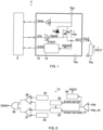
FIG. 1 is a block diagram of an integrated power supply including a sense circuit for monitoring operation and providing predictive maintenance indications about the load based upon the monitoring. -
FIG. 2 is a block diagram of the sense circuit ofFIG. 1 . -
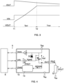
FIG. 3 is a graph showing the inputs and outputs of the integrated power supply during operation with loads having capacitive components. -
FIG. 4 is a block diagram of a version of the integrated power supply disclosed herein in which the power transistor is a p-channel transistor. -
FIG. 5 is a block diagram of a version of the integrated power supply disclosed herein in which the load is connected between the power supply voltage and the power transistor. -
FIG. 6 is a block diagram of a version of the integrated power supply disclosed herein in which the load is connected between the power supply voltage and the power transistor and in which the power transistor is a p-channel transistor. - The following disclosure enables a person skilled in the art to make and use the subject matter disclosed herein. The general principles described herein may be applied to embodiments and applications other than those detailed above without departing from the spirit and scope of this disclosure. This disclosure is not intended to be limited to the embodiments shown, but is to be accorded the widest scope consistent with the principles and features disclosed or suggested herein. Do note that in the below description, any described resistor or resistance is a discrete device unless the contrary is stated, and is not simply an electrical lead between two points. Thus, any described resistor or resistance coupled between two points has a greater resistance than a lead between those two points would have, and such resistor or resistance cannot be interpreted to be a lead. Similarly, any described capacitor or capacitance is a discrete device unless the contrary is stated, and is not a parasitic unless the contrary is stated. Moreover, any described inductor or inductance is a discrete device unless the contrary is stated, and is not a parasitic unless the contrary is stated.
- Now described with reference to
FIG. 1 is a power system 5 including an integratedpower supply 10 operating under control of a microcontroller (MCU) or application specific integrated circuit (ASIC) 6 to power aload 15. In various embodiments, theload 15 is a load with capacitive behavior, such as a purely capacitive load or a RC load or RLC load. - In the embodiment considered, the integrated
power supply 10 includes a n-channel power transistor MN having its drain connected to a power supply node Vdd, its source connected to an output node OUT, and its gate coupled to receive a drive signal Vgate from agate driver 11. Specifically, in various embodiments, the node power supply node Vdd is configured to receive a DC supply voltage and the output node OUT is configured to be connected to theload 15. For example, theload 15 may be connected between the output node OUT and a reference voltage Vss, such as a ground. - In various embodiments, a Zener diode DZ has its cathode connected to the drain of the transistor MN and its anode connected to the gate of the transistor MN, and serves, e.g., to short the drain and gate of the transistor MN for protection of the transistor MN when the voltage at its source goes negative (a typical consequence at switch-off of loads with inductive behaviour).
- In the embodiment considered, a
first sense circuit 13 is coupled to the source of the transistor MN to receive a current sensing input, and generates an overload protection output PROT to thedriver 11 and a diagnostic flag DIAG to the MCU or ASIC 5 as outputs. In various embodiments, asecond sense circuit 12 has its input connected to the supply node Vdd and generates a sense output Vsns to be provided to the MCU or ASIC 5. - Referring now to
FIG. 2 , in various embodiments, thesense circuit 13 includes acomparator 21 that has its non-inverting input terminal connected to the drain-to-source voltage Vds of the transistor MN, its inverting input terminal connected to a drain-to-source reference voltage Vds_ref, and its output connected (via a signal START/STOP) to acounter 22, (via a signal RESET/STORE) to aregister 23, and to aprotection circuit 29. Theregister 23 provides its currently held value Toverload as output to an inverting input terminal of adigital comparator 26 and a non-inverting input terminal of adigital comparator 27. Another input terminal of thedigital comparator 26 is coupled to receive a minimum overvoltage time Tovl(min), and another input terminal of thedigital comparator 27 is coupled to receive a maximum overvoltage time Tovl(max). An ORgate 28 receives the outputs of thecomparators - Operation will now be described. The MCU or ASIC 6 provides an input drive voltage VIN to the
gate driver 11. The input drive voltage VIN is digital, and from VIN, thegate driver 11 suitably generates the drive signal Vgate. The transistor MN operates based upon the drive signal Vdrive to power theload 15. - When the drain-to-source voltage Vds of the transistor MN exceeds the drain-to-source reference voltage Vds_ref, the
comparator 21 asserts its output, indicating that the output of power by the transistor MN to theload 15 has resulted in an overload condition. Based upon this output, theprotection circuit 29 generates a protection signal PROT fed to thegate driver 11 that causes thegate driver 11 to enter an overload protection mode and reduce the drive signal Vgate accordingly. Due to the capacitive behaviour of the load, as a result of the overload protection mode, the output current IOUT provided to the load is initially the maximum allowed by the control circuit and then decreases, while the output voltage VOUT increases accordingly. This may be observed in the graphs ofFIG. 3 , between times T1 and T2. - When the
comparator 21 asserts its output, that assertion acts as a START signal to thecounter 22 and acts as a RESET signal to theregister 23. Therefore, when Vds exceeds Vds_ref, the assertion of the output of thecomparator 21 causes the contents of theregister 23 to be reset and causes thecounter 22 to begin counting. In various embodiments, the circuit may also use a comparison window comprising two thresholds. In this case, the circuit may be configured to compare the drain-to-source voltage of the power transistor to a first threshold drain-to-source voltage, and begin counting when the drain-to-source voltage exceeds the first threshold, and end counting when the drain-to-source voltage no longer exceeds the first threshold drain-to-source voltage. Moreover, the circuit is configured to compare the drain-to-source voltage of the power transistor to a second threshold drain-to-source voltage, begin counting when the drain-to-source voltage falls below the second threshold drain-to-source voltage, and end counting when the drain-to-source voltage rises above the second threshold drain-to-source voltage. - When Vds falls back below Vds_ref, the output of the
comparator 21 is deasserted, indicating that the overload condition has ended. This deassertion of the output of thecomparator 21 causes theprotection circuit 29 to modify or cease the output of the protection signal PROT, allowing thegate driver 11 to enter back into normal operation. - This deassertion of the output of the
comparator 21 also acts as a STOP signal to thecounter 22, causing thecounter 22 to cease counting. The resulting total count is indicative of the duration of time for which the overload condition was present, and is stored as a value Toverload in theregister 23. - If Toverload is greater than a maximum overvoltage time Tovl(max), the
comparator 26 asserts its output. If Toverload is less than a minimum overvoltage time Tovl(min), thecomparator 27 asserts its output. Therefore, if Toverload - which is indicative of the duration of time for which the overload condition was present - is outside the window set by the maximum overvoltage time and the minimum overvoltage time, theOR gate 28 asserts the DIAG signal at its output, indicating the anomaly to the MCU or ASIC 6. The MCU or ASIC 6 may take subsequent action based upon assertion of the DIAG signal, such as providing output to another entity or to the user, or such as modifying (or ceasing) the output provided as the input voltage VIN to thegate driver 11. The providing of output to the user may take the form of activating an alert such, such as by activating a light emitting diode or audio output device controlled by the MCU or ASIC 6. - Additionally or alternatively, the total count Toverload may be read from the
register 23 by the MCU or ASIC 6, and each different received value of Toverload may be stored thereby to enable the taking of the subsequent action based upon the trend of the values of Toverload over time. For example, if Toverload has increased by a certain amount over a given number of iterations or if Toverload has decreased by a certain amount over a given number of iterations, the MCU or ASIC 6 may determine that maintenance of theload 15 is to be performed, and may take actions such as providing output to another entity or the user, such as modifying (or ceasing) the output provided as the input voltage VIN to thegate driver 11. The MCU or ASIC 6 may utilize self-learning based upon the values of Toverload over time, enabling updating of the values to which the changes in Toverload over time are compared to, improving efficiency of the predictive maintenance. - In various embodiments, the maximum overvoltage time Tovl(max) and minimum overvoltage time Tovl(min) may be set by the MCU or ASIC 6 based upon the electrical characteristics (resistance, capacitance, etc) of the
load 15, as well as safe operating conditions (e.g., safe drain current) of the transistor MN. For example, the maximum overvoltage time Tovl(max) and minimum overvoltage time Tovl(min) may be set to be such that when the maximum overvoltage time is exceeded, or when the minimum overvoltage time is not met, this is indicative of degradation of theload 15 sufficient to warrant inspection and maintenance but as of yet insufficient to result in malfunction of theload 15. This way, preventative maintenance can be scheduled, avoiding excess downtime of the load (which may be a machine within a factory), potentially avoiding a downstream malfunction causes by malfunction of the load. - In various embodiments, when an overload condition occurs and the DIAG signal is asserted, the MCU or ASIC 6 checks whether an overvoltage condition is present on Vsns, since the overload condition could be a consequence of an overvoltage condition on the supply voltage Vdd. Therefore, the MCU or ASIC 6 may be set to ignore assertions of the DIAG signal resulting from cases where the overload condition was not caused by the
load 15. - It is clear that modifications and variations may be made to what has been described and illustrated herein, without thereby departing from the scope of this disclosure, as defined in the annexed claims. For example, in the above disclosure, the transistor MN is an n-channel transistor, but may instead be a p-channel transistor MP, as shown in
FIG. 4 . In addition, in the above disclosure, theload 15 is a low-side load, but may instead be a high-side load, as shown inFIG. 5 in which theload 15 is connected between Vdd and the drain of MN, indicated as node IN. Still further, the transistor may be a p-channel transistor MP and theload 15 may be a high-side load with theload 15 being connected between Vdd and the source of MP, as shown inFIG. 6 . - While the disclosure has been described with respect to a limited number of embodiments, those skilled in the art, having benefit of this disclosure, will appreciate that other embodiments can be envisioned that do not depart from the scope of the disclosure as disclosed herein. Accordingly, the scope of the disclosure shall be limited only by the attached claims.
Claims (16)
- A system (5), comprising:- a power transistor (MN) having a first conduction terminal coupled to a supply node (VDD), a second conduction terminal coupled to a load node (OUT, IN), and a control terminal controlled by a drive signal (Vgate);- a driver (11) configured to receive an input voltage (VIN) from an external component (6) and generate the drive signal based thereupon;- a sense circuit (13) configured to, when the power transistor is powering a load (15) coupled to the load node:- detect whether the power transistor has entered an overload condition, and if so, determine a duration of time that the power transistor is in the overload condition; and- assert a diagnostic signal (DIAG) in response to the duration of time being outside of a time window.
- The system of claim 1, wherein the time window is defined by a maximum time, a minimum time, or both a maximum and a minimum time.
- The system of claim 1, wherein the sense circuit (13) is further configured to assert the diagnostic signal (DIAG) in response to the duration of time being less than a minimum period of time.
- The system of claim 1, wherein the sense circuit (13) is further configured to assert the diagnostic signal in response to the duration of time being greater than a maximum period of time.
- The system of claim 1, wherein the sense circuit (13) comprises:- a first comparator (21) configured to compare a voltage (Vds) across the first and second conduction terminal of the power transistor (MN) to a reference voltage (Vds_Ref) and assert its output to indicate that the power transistor has entered the overload condition if the voltage across the first and second conduction terminals exceeds the reference voltage;- a counter (22) configured to start in response to assertion of the output of the first comparator, and to stop at a final count in response to deassertion of the output of the first comparator; and- a comparison circuit (23, 24, 25, 26, 27, 28) configured to compare the final count to a threshold count (24, 25) indicative of time window and assert the diagnostic signal based thereupon.
- The system of claim 5, wherein:- the comparison circuit (13) compares the final count to an upper threshold count (25) indicative of a maximum period of time and asserts the diagnostic signal (DIAG) if the final count is greater than the upper threshold count, with the upper threshold count being indicative of the time window; or- the comparison circuit (13) compares the final count to a lower threshold count (24) indicative of a minimum period of time and asserts the diagnostic signal (DIAG) if the final count is lower than the lower threshold count, with the lower threshold count being indicative of the time window; or- the comparison circuit (13) compares the final count to an upper threshold count (25) and a lower threshold count (24) and asserts the diagnostic signal (DIAG) if the final count is greater than the upper threshold count or lower than the lower threshold count, wherein the time window is defined by the upper threshold count and the lower threshold count.
- The system of claim 5, wherein the comparison circuit (23, 24, 25, 26, 27, 28) comprises:- a first digital comparator (27) configured to receive as input the upper threshold count (25) and the final count, and to assert its output if the final count is greater than the upper threshold count;- a second digital comparator (26) configured to receive as input the lower threshold count (24) and the final count, and to assert its output if the final count is less than the lower threshold count; and- a logic circuit (28) configured to assert the diagnostic signal (DIAG) in response to assertion of either the output of the first digital comparator or the output of the second digital comparator.
- The system of claim 5, wherein the sense circuit (13) further comprises: a protection circuit (29) configured to instruct the driver (MN) to modify the drive signal (Vgate) in response to assertion of the output of the first comparator (27) and to cease such instruction in response to deassertion of the output of the first comparator.
- The system of claim 1, wherein the external component (6) is a controller configured to generate the input voltage, configured to receive the diagnostic signal (DIAG), and configured to modify the input voltage based upon assertion of the diagnostic signal.
- The system of claim 1,wherein the load node (OUT, IN) is an output node (OUT); wherein the power transistor (MN) comprises an n-channel transistor, with the first conduction terminal being a drain, with the second conduction terminal being a source, and with the control terminal being a gate; and wherein the sense circuit (13) detects whether the power transistor has entered the overload condition by determining that a drain-to-source voltage (Vds) of the power transistor exceeds a reference drain-to-source voltage (Vds_ref); orwherein the load node (OUT, IN) is an input node (IN); wherein the power transistor (MN) comprises an n-channel transistor, with the second conduction terminal being a drain, with the first conduction terminal being a source, and with the control terminal being a gate; and wherein the sense circuit detects whether the power transistor has entered the overload condition by determining that a drain-to-source voltage (Vds) of the power transistor exceeds a reference drain-to-source voltage (Vds_ref); orwherein the load node (OUT, IN) is an output node (OUT); wherein the power transistor (MP) comprises a p-channel transistor with the first conduction terminal being a source, the second conduction terminal being a drain, and with the control terminal being a gate; and wherein the sense circuit detects whether the power transistor has entered the overload condition by determining that a source-to-drain voltage (Vds) of the power transistor exceeds a reference source-to-drain voltage (Vds_Ref).
- The system of claim 1, further comprising a supply sense circuit (12) configured to sense a supply voltage (Vdd) at the supply node and output the sensed supply voltage (Vsns); and wherein the external component is a controller configured to: generate the input voltage, receive the diagnostic signal, and modify the input voltage based upon assertion of the diagnostic signal unless the sensed supply voltage is indicative of an overvoltage condition at the supply node.
- A method of operating a system of any of the previous claims, comprising:- while the power transistor (MN) enables powering a load (15), detecting whether the power transistor (MN) has entered into an overload condition, and if so, determining a duration of time that the power transistor is in the overload condition;- making a determination of whether maintenance of the load is to be performed (DIAG) based upon the duration of time; and- taking subsequent action based upon the maintenance determination, such as turning on a light emitting diode or activating an audio output device.
- The method of claim 12, wherein the determination of whether maintenance of the load is to be performed is made by determining whether the duration of time exceeds a threshold determination of time.
- The method of claim 12, wherein the determination of whether maintenance of the load is to be performed is made by determining whether the duration of time has changed in value as compared to a prior duration of time during which the power transistor was previously in the overload condition by more than a given amount.
- The method of claim 12, wherein determining the duration of time that the power transistor is in the overload condition is performed by:- comparing a drain-to-source voltage (Vds) of the power transistor (MN) to a first threshold drain-to-source voltage (Vds_ref), beginning counting when the drain-to-source voltage exceeds the first threshold drain-to-source voltage, and ending counting when the drain-to-source voltage no longer exceeds the first threshold drain-to-source voltage; and/or- comparing a drain-to-source voltage (Vds) of the power transistor (MN) to a second threshold drain-to-source voltage (Vds_ref), beginning counting when the drain-to-source voltage falls below the second threshold drain-to-source voltage, and ending counting when the drain-to-source voltage rises above the second threshold drain-to-source voltage.
- The method of claim 12, wherein the determining of whether the maintenance of the load is to be performed is based upon the duration of time and whether an overvoltage condition is present on a supply node; and wherein the subsequent action is not taken if the overvoltage condition is present on the supply node.
Applications Claiming Priority (1)
| Application Number | Priority Date | Filing Date | Title |
|---|---|---|---|
| US17/866,701 US12140982B2 (en) | 2022-07-18 | 2022-07-18 | Time based predictive maintenance for capacitive loads in factory automation applications |
Publications (1)
| Publication Number | Publication Date |
|---|---|
| EP4310515A1 true EP4310515A1 (en) | 2024-01-24 |
Family
ID=87377958
Family Applications (1)
| Application Number | Title | Priority Date | Filing Date |
|---|---|---|---|
| EP23185933.1A Withdrawn EP4310515A1 (en) | 2022-07-18 | 2023-07-17 | Time based predictive maintenance for capacitive loads in factory automation applications |
Country Status (3)
| Country | Link |
|---|---|
| US (1) | US12140982B2 (en) |
| EP (1) | EP4310515A1 (en) |
| CN (1) | CN117424176A (en) |
Families Citing this family (3)
| Publication number | Priority date | Publication date | Assignee | Title |
|---|---|---|---|---|
| US12140982B2 (en) * | 2022-07-18 | 2024-11-12 | Stmicroelctronics S.R.L. | Time based predictive maintenance for capacitive loads in factory automation applications |
| US12267071B2 (en) * | 2023-06-01 | 2025-04-01 | Allegro Microsystems, Llc | Desaturation circuit having temperature compensation |
| CN117895450A (en) * | 2024-03-15 | 2024-04-16 | 中车南京浦镇车辆有限公司 | DC bus power supply circuit and over-voltage and under-voltage protection method |
Citations (2)
| Publication number | Priority date | Publication date | Assignee | Title |
|---|---|---|---|---|
| US20110110009A1 (en) * | 2009-11-12 | 2011-05-12 | Anden Co., Ltd. | Switch circuit having overcurrent detection function |
| US20170294154A1 (en) * | 2016-04-06 | 2017-10-12 | Rohm Co., Ltd. | Overcurrent detection circuit |
Family Cites Families (20)
| Publication number | Priority date | Publication date | Assignee | Title |
|---|---|---|---|---|
| US4301490A (en) | 1979-07-09 | 1981-11-17 | American Standard Inc. | Electronic overload protection circuit |
| JP2005323413A (en) | 2004-05-06 | 2005-11-17 | Rohm Co Ltd | Overcurrent detection circuit and power supply comprising it |
| US7453709B2 (en) * | 2005-07-08 | 2008-11-18 | Power Integrations, Inc. | Method and apparatus for increasing the power capability of a power supply |
| FR2927479B1 (en) | 2008-02-08 | 2012-05-04 | Schneider Electric Ind Sas | SYSTEM FOR CONTROLLING AND PROTECTING A NEGATIVE LOGIC OUTPUT OF AN AUTOMATION EQUIPMENT. |
| US20120206122A1 (en) * | 2011-02-11 | 2012-08-16 | Timothy Alan Dhuyvetter | Constant off time boost converter |
| US9459304B1 (en) | 2012-08-08 | 2016-10-04 | Perry Parkin | Method of fault prediction for electrical distribution systems and monitored loads |
| JP6073692B2 (en) * | 2013-01-23 | 2017-02-01 | ルネサスエレクトロニクス株式会社 | Motor drive control device and operation method thereof |
| US9966943B2 (en) * | 2016-03-31 | 2018-05-08 | Infineon Technologies Ag | System and method for a high-side power switch |
| US10541617B2 (en) * | 2016-06-02 | 2020-01-21 | Semiconductor Components Industries, Llc | Overload protection for power converter |
| US10720846B2 (en) * | 2017-01-05 | 2020-07-21 | Dialog Semiconductor Inc. | Sense resistor short detection for switching power converters |
| FR3068836B1 (en) * | 2017-07-07 | 2019-08-23 | Stmicroelectronics (Rousset) Sas | PROTECTIVE CIRCUIT FOR A POWER SWITCH |
| CN110945772B (en) * | 2017-07-31 | 2022-11-18 | 罗姆股份有限公司 | Current detection circuit |
| US11675379B2 (en) * | 2018-09-14 | 2023-06-13 | Intel Corporation | Variable-adaptive integrated computational digital low dropout regulator |
| US10756640B1 (en) * | 2019-03-28 | 2020-08-25 | Appulse Power Inc. | Flyback converter with synchronous rectifier controller |
| US10895601B2 (en) * | 2019-05-10 | 2021-01-19 | Infineon Technologies Ag | System and method of monitoring a switching transistor |
| CN209994092U (en) | 2019-06-25 | 2020-01-24 | 汉纳森(厦门)数据股份有限公司 | Vehicle and overload protection circuit of vehicle |
| US11316335B2 (en) | 2020-04-30 | 2022-04-26 | GM Global Technology Operations LLC | Active disconnect device |
| US11728731B2 (en) * | 2020-05-09 | 2023-08-15 | Intel Corporation | Accurate load current sensing apparatus and method |
| US12164319B2 (en) * | 2020-12-19 | 2024-12-10 | Intel Corporation | Dual loop voltage regulator |
| US12140982B2 (en) * | 2022-07-18 | 2024-11-12 | Stmicroelctronics S.R.L. | Time based predictive maintenance for capacitive loads in factory automation applications |
-
2022
- 2022-07-18 US US17/866,701 patent/US12140982B2/en active Active
-
2023
- 2023-07-17 CN CN202310873953.8A patent/CN117424176A/en active Pending
- 2023-07-17 EP EP23185933.1A patent/EP4310515A1/en not_active Withdrawn
Patent Citations (2)
| Publication number | Priority date | Publication date | Assignee | Title |
|---|---|---|---|---|
| US20110110009A1 (en) * | 2009-11-12 | 2011-05-12 | Anden Co., Ltd. | Switch circuit having overcurrent detection function |
| US20170294154A1 (en) * | 2016-04-06 | 2017-10-12 | Rohm Co., Ltd. | Overcurrent detection circuit |
Also Published As
| Publication number | Publication date |
|---|---|
| US12140982B2 (en) | 2024-11-12 |
| CN117424176A (en) | 2024-01-19 |
| US20240019885A1 (en) | 2024-01-18 |
Similar Documents
| Publication | Publication Date | Title |
|---|---|---|
| US12140982B2 (en) | Time based predictive maintenance for capacitive loads in factory automation applications | |
| US9263937B2 (en) | Short protection circuit for power switch and associated protection method | |
| US9966943B2 (en) | System and method for a high-side power switch | |
| US9608509B2 (en) | Switching converter with controllable restart delay and associated control method | |
| US7885048B2 (en) | Semiconductor device and an electronic apparatus incorporating the semiconductor device | |
| US7550955B2 (en) | Power supply circuit | |
| US20170070222A1 (en) | Adaptive blanking timer for short circuit detection | |
| CN113740690B (en) | Secondary side controller for flyback converter and method for detecting fault condition | |
| TWI632765B (en) | DC-DC transformer | |
| KR20110103252A (en) | Driving method of power factor correction circuit and power factor correction circuit | |
| US10243344B2 (en) | Semiconductor device | |
| CN101188381A (en) | DC-DC Converter | |
| US7986149B2 (en) | System and method for adaptive load fault detection | |
| US9030249B2 (en) | Level shift circuit | |
| US9817077B2 (en) | Circuit device and electronic apparatus | |
| TWI688194B (en) | Power supply circuit | |
| CN105322810A (en) | Power conversion device and protection method thereof when current feedback signal is abnormal | |
| CN110557106A (en) | Switch unit turn-off protection circuit and protection method | |
| US10008935B2 (en) | DC-DC converter | |
| US12334826B2 (en) | Peak current limit management for high frequency buck converter | |
| JP2006115594A (en) | Malfunction prevention circuit | |
| JP2021044645A (en) | Short-circuit detection circuit | |
| JP6983718B2 (en) | Voltage regulator | |
| CN207753898U (en) | A kind of output overvoltage protection circuit based on floating ground BUCK frameworks | |
| CN114814530A (en) | An open-load detection circuit, method and application for high-side intelligent power IC |
Legal Events
| Date | Code | Title | Description |
|---|---|---|---|
| PUAI | Public reference made under article 153(3) epc to a published international application that has entered the european phase |
Free format text: ORIGINAL CODE: 0009012 |
|
| STAA | Information on the status of an ep patent application or granted ep patent |
Free format text: STATUS: THE APPLICATION HAS BEEN PUBLISHED |
|
| AK | Designated contracting states |
Kind code of ref document: A1 Designated state(s): AL AT BE BG CH CY CZ DE DK EE ES FI FR GB GR HR HU IE IS IT LI LT LU LV MC ME MK MT NL NO PL PT RO RS SE SI SK SM TR |
|
| STAA | Information on the status of an ep patent application or granted ep patent |
Free format text: STATUS: THE APPLICATION HAS BEEN WITHDRAWN |
|
| 18W | Application withdrawn |
Effective date: 20240628 |