EP4307561A1 - Doherty amplifier - Google Patents
Doherty amplifier Download PDFInfo
- Publication number
- EP4307561A1 EP4307561A1 EP21936993.1A EP21936993A EP4307561A1 EP 4307561 A1 EP4307561 A1 EP 4307561A1 EP 21936993 A EP21936993 A EP 21936993A EP 4307561 A1 EP4307561 A1 EP 4307561A1
- Authority
- EP
- European Patent Office
- Prior art keywords
- amplifier
- input signal
- output
- frequency band
- filter circuit
- Prior art date
- Legal status (The legal status is an assumption and is not a legal conclusion. Google has not performed a legal analysis and makes no representation as to the accuracy of the status listed.)
- Granted
Links
Images




Classifications
-
- H—ELECTRICITY
- H03—ELECTRONIC CIRCUITRY
- H03F—AMPLIFIERS
- H03F1/00—Details of amplifiers with only discharge tubes, only semiconductor devices or only unspecified devices as amplifying elements
- H03F1/02—Modifications of amplifiers to raise the efficiency, e.g. gliding Class A stages, use of an auxiliary oscillation
- H03F1/0205—Modifications of amplifiers to raise the efficiency, e.g. gliding Class A stages, use of an auxiliary oscillation in transistor amplifiers
- H03F1/0288—Modifications of amplifiers to raise the efficiency, e.g. gliding Class A stages, use of an auxiliary oscillation in transistor amplifiers using a main and one or several auxiliary peaking amplifiers whereby the load is connected to the main amplifier using an impedance inverter, e.g. Doherty amplifiers
-
- H—ELECTRICITY
- H03—ELECTRONIC CIRCUITRY
- H03F—AMPLIFIERS
- H03F1/00—Details of amplifiers with only discharge tubes, only semiconductor devices or only unspecified devices as amplifying elements
- H03F1/56—Modifications of input or output impedances, not otherwise provided for
-
- H—ELECTRICITY
- H03—ELECTRONIC CIRCUITRY
- H03F—AMPLIFIERS
- H03F3/00—Amplifiers with only discharge tubes or only semiconductor devices as amplifying elements
- H03F3/189—High-frequency amplifiers, e.g. radio frequency amplifiers
- H03F3/19—High-frequency amplifiers, e.g. radio frequency amplifiers with semiconductor devices only
- H03F3/193—High-frequency amplifiers, e.g. radio frequency amplifiers with semiconductor devices only with field-effect devices
-
- H—ELECTRICITY
- H03—ELECTRONIC CIRCUITRY
- H03F—AMPLIFIERS
- H03F3/00—Amplifiers with only discharge tubes or only semiconductor devices as amplifying elements
- H03F3/20—Power amplifiers, e.g. Class B amplifiers, Class C amplifiers
- H03F3/24—Power amplifiers, e.g. Class B amplifiers, Class C amplifiers of transmitter output stages
- H03F3/245—Power amplifiers, e.g. Class B amplifiers, Class C amplifiers of transmitter output stages with semiconductor devices only
-
- H—ELECTRICITY
- H03—ELECTRONIC CIRCUITRY
- H03F—AMPLIFIERS
- H03F3/00—Amplifiers with only discharge tubes or only semiconductor devices as amplifying elements
- H03F3/68—Combinations of amplifiers, e.g. multi-channel amplifiers for stereophonics
-
- H—ELECTRICITY
- H03—ELECTRONIC CIRCUITRY
- H03F—AMPLIFIERS
- H03F2200/00—Indexing scheme relating to amplifiers
- H03F2200/222—A circuit being added at the input of an amplifier to adapt the input impedance of the amplifier
-
- H—ELECTRICITY
- H03—ELECTRONIC CIRCUITRY
- H03F—AMPLIFIERS
- H03F2200/00—Indexing scheme relating to amplifiers
- H03F2200/387—A circuit being added at the output of an amplifier to adapt the output impedance of the amplifier
-
- H—ELECTRICITY
- H03—ELECTRONIC CIRCUITRY
- H03F—AMPLIFIERS
- H03F2200/00—Indexing scheme relating to amplifiers
- H03F2200/423—Amplifier output adaptation especially for transmission line coupling purposes, e.g. impedance adaptation
-
- H—ELECTRICITY
- H03—ELECTRONIC CIRCUITRY
- H03F—AMPLIFIERS
- H03F2200/00—Indexing scheme relating to amplifiers
- H03F2200/451—Indexing scheme relating to amplifiers the amplifier being a radio frequency amplifier
Definitions
- the present disclosure relates to a Doherty amplifier that operates in multiple frequency bands.
- PAPR peak to average power ratio
- Patent Literature 1 As an amplifier that amplifies a signal for communications with a high degree of efficiency, a Doherty amplifier is proposed in Patent Literature 1.
- the Doherty amplifier shown in Patent Literature 1 is one in which a control unit switches the class of operation for each of first and second amplifying elements in accordance with whether the operating frequency of an input signal is a first operating frequency or a second operating frequency.
- Patent Literature 1 WO 2019/09760
- the present disclosure is provided in view of the above-mentioned point, and it is an object of the present disclosure to provide a Doherty amplifier that operates in multiple frequency bands without having to control the amplifying elements which constitute the Doherty amplifier.
- a Doherty amplifier includes: a first filter circuit to, when an input signal lying in a first frequency band is inputted, output a first input signal obtained by attenuating the input signal lying in the first frequency band by a first amount of attenuation, and to, when an input signal lying in a second frequency band different from the first frequency band is inputted, output a second input signal obtained by allowing passage of the input signal lying in the second frequency band; a second filter circuit to, when an input signal lying in the first frequency band is inputted, output a third input signal obtained by attenuating the input signal lying in the first frequency band by a second amount of attenuation smaller than the first amount of attenuation, and to, when an input signal lying in the second frequency band is inputted, output a fourth input signal obtained by attenuating the input signal lying in the second frequency band by a third amount of attenuation larger than or equal to the first amount of attenuation; a first amplifier in which a gate bias voltage is fixed, to operate as
- the Doherty amplifier operates in the multiple frequency bands without having to control the first amplifier and the second amplifier.
- a Doherty amplifier according to Embodiment 1 will be explained on the basis of FIGS. 1 to 10 .
- the Doherty amplifier operates in two operating frequency bands: a first frequency band and a second frequency band.
- the first frequency band and the second frequency band are different frequency ranges, and the first frequency band is a frequency range lower than the second frequency band.
- the first frequency band is referred to as a low frequency range showing a frequency range lower than the second frequency band
- the second frequency band is referred to as a high frequency range showing a frequency range higher than the first frequency band.
- a gate bias voltage applied to each of two amplifiers in parallel is fixed to one at which each of the amplifiers operates as a class B amplifier, and two filter circuits connected as stages preceding the two parallel amplifiers cause each of the two parallel amplifiers to switch between a main amplifier function and an auxiliary amplifier function according to the two operating frequency bands in which the pass losses in these operating frequency bands are made to differ from each other.
- two amplifiers main and auxiliary amplifiers with equal saturation output power are connected in parallel.
- Input signals inputted to the two parallel amplifiers satisfy a relation showing that when a second frequency in the second frequency band is assumed to be 1.0, a first frequency in the first frequency band is 0.5 with respect to the second frequency.
- the Doherty amplifier includes, between an input terminal 1 and an output terminal 2, a third input matching circuit 3, a splitter 4, a phase correction circuit 5, a first filter circuit 6a, a second filter circuit 6b, a first input matching circuit 7a, a second input matching circuit 7b, the two parallel amplifiers 8 having a first amplifier 8a and a second amplifier 8b, an output combination circuit 9 having a first output circuit 9a and a second output circuit 9b, and an output matching circuit 10.
- the third input matching circuit 3 is connected between the input terminal 1 and an input end of the splitter 4, and performs impedance matching between the input terminal 1 and the splitter 4.
- the third input matching circuit 3 is an impedance matching network (IMN) that includes a matching circuit using a lumped constant element, a matching circuit using a distributed constant line, a matching circuit which is a combination of a lumped constant and a distributed constant, a matching circuit using an LC matching circuit, or the like.
- INN impedance matching network
- the splitter 4 has an input end connected to an output end of the third input matching circuit 3, an output end connected to an input end of the phase correction circuit 5, and another output end connected to the second filter circuit 6b, and splits an input signal inputted thereto from the input terminal 1 to an input signal at the output end thereof and an input signal at the other output end thereof.
- the splitter 4 is a Wilkinson splitter, a hybrid circuit, or the like which is comprised of a circuit using a lumped constant element, a circuit using a distributed constant line, a circuit which is a combination of a lumped constant and a distributed constant, a circuit using an LC matching circuit, or the like.
- the phase correction circuit 5 is connected between the output end of the splitter 4 and an input end of the first filter circuit 6a, and causes the electric length from the output end of the splitter 4 to an output combination point 9A which is an output end of the output combination circuit 9, i.e., the electric length of a path on a side of the first amplifier 8a to be equal to the electric length from the other output end of the splitter 4 to the output combination point 9A of the output combination circuit 9, i.e., the electric length of a path on a side of the second amplifier 8b.
- the phase correction circuit 5 is comprised of a circuit using a lumped constant element, a circuit using a distributed constant line, a circuit which is a combination of a lumped constant and a distributed constant, a circuit using an LC matching circuit, or the like.
- the input end of the first filter circuit 6a is connected to an output end of the phase correction circuit 5, and the first filter circuit 6a receives the input signal outputted from the output end of the splitter 4 and inputted thereto via the phase correction circuit 5.
- the first filter circuit 6a When an input signal lying in the first frequency band is inputted, the first filter circuit 6a outputs a first input signal obtained by attenuating the input signal lying in the first frequency band by a first amount of attenuation XdB, and when an input signal lying in the second frequency band is inputted, the first filter circuit 6a outputs a second input signal obtained by allowing passage of the input signal lying in the second frequency band.
- the first filter circuit 6a When the input signal lies in the first frequency band, the first filter circuit 6a outputs a signal having a small amplitude because the first input signal is attenuated by XdB, and when the input signal lies in the second frequency band, the first filter circuit 6a outputs a signal having a large amplitude because the second input signal is not attenuated.
- the above-mentioned amplitude of the input signal refers to the amplitude of the envelope of the signal.
- the amplitude of an input signal which will be explained below, also refers to the amplitude of the envelope of the signal.
- the first filter circuit 6a is a high pass filter circuit in which the amount of attenuation in the first frequency band is set to XdB, and the amount of attenuation in the second frequency band is set to 0dB (passage), as shown by a solid line A in FIG. 4 .
- the first filter circuit 6a is a reactive high pass filter circuit comprised of a reactive reflection loss, such as a filter circuit using a lumped constant element, a filter circuit using a distributed constant line, a filter circuit which is a combination of a lumped constant and a distributed constant, or a filter circuit using an LC matching circuit.
- a reactive reflection loss such as a filter circuit using a lumped constant element, a filter circuit using a distributed constant line, a filter circuit which is a combination of a lumped constant and a distributed constant, or a filter circuit using an LC matching circuit.
- the downsizing of the first filter circuit 6a can be achieved.
- a resistive high pass filter circuit such as an attenuator, instead of a reactive high pass filter circuit, may be used.
- the second filter circuit 6b has an input end connected to the other output end of the splitter 4, and receives the input signal outputted from the other output end of the splitter 4 and inputted thereto.
- the second filter circuit 6b When an input signal lying in the first frequency band is inputted, the second filter circuit 6b outputs a third input signal obtained by allowing passage of the input signal lying in the first frequency band, and when an input signal lying in the second frequency band is inputted, the second filter circuit 6b outputs a fourth input signal obtained by attenuating the input signal lying in the second frequency band by the first amount of attenuation XdB.
- the second filter circuit 6b When the input signal lies in the first frequency band, the second filter circuit 6b outputs a signal having a large amplitude because the third input signal is not attenuated, and when the input signal lies in the second frequency band, the second filter circuit 6b outputs a signal having a small amplitude because the fourth input signal is attenuated by XdB.
- the second filter circuit 6b is a low pass filter circuit in which the amount of attenuation in the first frequency band is set to 0dB (passage), and the amount of attenuation in the second frequency band is set to XdB, as shown by a solid line B in FIG. 4 .
- the second filter circuit 6b is a reactive low pass filter circuit comprised of a reactive reflection loss, such as a filter circuit using a lumped constant element, a filter circuit using a distributed constant line, a filter circuit which is a combination of a lumped constant and a distributed constant, or a filter circuit using an LC matching circuit.
- a reactive reflection loss such as a filter circuit using a lumped constant element, a filter circuit using a distributed constant line, a filter circuit which is a combination of a lumped constant and a distributed constant, or a filter circuit using an LC matching circuit.
- the downsizing of the second filter circuit 6b can be achieved.
- a resistive low pass filter circuit such as an attenuator, instead of a reactive low pass filter circuit, may be used.
- the second filter circuit 6b may output, as the third input signal, the signal which the second filter circuit attenuates by a second amount of attenuation smaller than the first amount of attenuation XdB.
- the second filter circuit 6b may output, as the fourth input signal, the signal which the second filter circuit attenuates by a third amount of attenuation larger than or equal to the first amount of attenuation XdB.
- the amount of attenuation XdB in the first filter circuit 6a with respect to the first frequency band and the amount of attenuation XdB in the second filter circuit 6b with respect to the second frequency band are set to 6dB, as an example, when it is desirable to improve the efficiency of each of the first and second amplifiers 8a and 8b, or are set to 3dB, as an example, when it is desirable to balance the efficiency and linearity of each of the first and second amplifiers 8a and 8b.
- the first input matching circuit 7a is an impedance matching network (IMN) which is connected between an output end of the first filter circuit 6a and an input end 8a1 of the first amplifier 8a, and which performs input matching with the first amplifier 8a.
- IPN impedance matching network
- the first input matching circuit 7a is an impedance matching network (IMN) which is comprised of a matching circuit using a lumped constant element, a matching circuit using a distributed constant line, a matching circuit which is a combination of a lumped constant and a distributed constant, a matching circuit using an LC matching circuit, or the like.
- INN impedance matching network
- the first input matching circuit 7a may be connected between the output end of the phase correction circuit 5 and the input end of the first filter circuit 6a.
- the second input matching circuit 7b is an impedance matching network (IMN) which is connected between an output end of the second filter circuit 6b and an input end 8b 1 of the second amplifier 8b, and which performs input matching with the second amplifier 8b.
- IPN impedance matching network
- the second input matching circuit 7b is an impedance matching network (IMN) which is comprised of a matching circuit using a lumped constant element, a matching circuit using a distributed constant line, a matching circuit which is a combination of a lumped constant and a distributed constant, a matching circuit using an LC matching circuit, or the like.
- INN impedance matching network
- the second input matching circuit 7b may be connected between the other output end of the splitter 4 and the input end of the second filter circuit 6b.
- the two parallel amplifiers 8 is comprised of the first amplifier 8a and the second amplifier 8b, and each of the first and second amplifiers 8a and 8b is biased to a threshold voltage at which each of the amplifiers operates as a class B amplifier, i.e., the threshold voltage of a transistor which constitutes each of the first and second amplifiers 8a and 8b.
- the threshold voltage in the present disclosure contains the value of the threshold voltage itself and even a plus or minus design tolerance value with respect to the value of the threshold voltage.
- the input end 8a1 of the first amplifier 8a is connected to a gate bias terminal 11a at which the gate bias voltage is fixed, and when the first input signal outputted from the first filter circuit 6a is inputted to the input end 8a1 via the first input matching circuit 7a, the first amplifier 8a starts at a time later than the second amplifier 8b and operates as the auxiliary amplifier because the amplitude of the first input signal is smaller than the amplitude of the third input signal, whereas when the second input signal outputted from the first filter circuit 6a is inputted to the input end 8a1, the first amplifier 8a starts at a time earlier than the second amplifier 8b and operates as the main amplifier because the amplitude of the second input signal is larger than the amplitude of the fourth input signal.
- the first amplifier 8a operates as the auxiliary amplifier when the input signal inputted to the input terminal 1 lies in the first frequency band, whereas the first amplifier 8a operates as the main amplifier when the input signal inputted to the input terminal 1 lies in the second frequency band.
- the saturation output power when operating as the main amplifier and the saturation output power when operating as the auxiliary amplifier are equal.
- a transistor such as a field effect transistor (FET), a heterojunction bipolar transistor (HBT), or a high electron mobility transistor (HEMT) is used.
- FET field effect transistor
- HBT heterojunction bipolar transistor
- HEMT high electron mobility transistor
- the first amplifier 8a may include circuit configuration elements needed as the amplifier, such as a stabilization circuit connected to an input side of the transistor and a bias circuit connected to an output side of the transistor.
- the transistor as the first amplifier 8a has a gate electrode serving as the input end 8a1, a drain electrode serving as an output end 8a2 and connected, via a load resistor, to a power supply potential Vcc, and a source electrode connected to a ground node.
- the input end 8a1 is connected to the gate bias terminal 11a, and the gate bias terminal 11a is connected to the power supply potential Vcc via a resistive element (bias resister).
- the threshold voltage of the transistor is applied to the gate bias terminal 1 1a in such a way that the transistor as the first amplifier 8a operates as a class B amplifier.
- FIG. 2 An equivalent circuit of the first amplifier 8a is shown in FIG. 2 . More specifically, it is assumed that the first amplifier 8a is comprised of a current source Ia which is based on a current flowing between the drain and the source of the transistor, and an output capacitance Ca which is a parasitic capacitance between the drain of the transistor and the ground.
- the output capacitance Ca of the first amplifier 8a is compensated for by an inductor or the like or incorporated as a part of the first output circuit 9a, and the current source Ia is connected directly to the first output circuit 9a from the viewpoint of electric lengths.
- the input end 8b 1 of the second amplifier 8b is connected to a gate bias terminal 11b at which the gate bias voltage is fixed, and when the third input signal outputted from the second filter circuit 6b is inputted to the input end 8b 1 via the second input matching circuit 7b, the second amplifier 8b starts at a time earlier than the first amplifier 8a and operates as the main amplifier because the amplitude of the third input signal is larger than the amplitude of the first input signal, whereas when the fourth input signal outputted from the second filter circuit 6b is inputted to the input end 8b 1, the second amplifier 8b starts at a time later than the second amplifier 8b and operates as the auxiliary amplifier because the amplitude of the fourth input signal is smaller than the amplitude of the second input signal.
- the second amplifier 8b operates as the main amplifier when the input signal inputted to the input terminal 1 lies in the first frequency band, whereas the second amplifier 8b operates as the auxiliary amplifier when the input signal inputted to the input terminal 1 lies in the second frequency band.
- the saturation output power when operating as the main amplifier and the saturation output power when operating as the auxiliary amplifier are equal.
- a transistor such as an FET, an HBT, or a HEMT is used.
- the second amplifier 8b may include circuit configuration elements needed as the amplifier, such as a stabilization circuit connected to an input side of the transistor and a bias circuit connected to an output side of the transistor.
- the transistor as the second amplifier 8b has a gate electrode serving as the input end 8b 1, a drain electrode serving as an output end 8b2 and connected, via a load resistor, to the power supply potential Vcc, and a source electrode connected to a ground node.
- the input end 8b1 is connected to the gate bias terminal 11b, and the gate bias terminal 11b is connected to the power supply potential Vcc via a resistive element (bias resister).
- the threshold voltage of the transistor is applied to the gate bias terminal 11b in such a way that the transistor as the first amplifier 8a operates as a class B amplifier.
- the gate bias terminal 11b may also serve as the gate bias terminal 11a.
- FIG. 3 An equivalent circuit of the second amplifier 8b is shown in FIG. 3 . More specifically, it is assumed that the second amplifier 8b is comprised of: a current source Ib which is based on a current flowing between the drain and the source of the transistor; and an output capacitance Cb which is a parasitic capacitance between the drain of the transistor and the ground.
- the output capacitance Cb of the second amplifier 8b is compensated for by an inductor or the like or incorporated as a part of the second output circuit 9b, and the current source Ib is connected directly to the second output circuit 9b from the viewpoint of electric lengths.
- the times that the first amplifier 8a and the second amplifier 8b start differ because the amplitudes of the input signals inputted to the first amplifier 8a and the second amplifier 8b differ because of the first filter circuit 6a and the second filter circuit 6b.
- the output load impedances of the first amplifier 8a and the second amplifier 8b differ.
- the time that the second amplifier 8b starts is earlier than the time that the first amplifier 8a starts, and the second amplifier 8b functions as the main amplifier while the first amplifier 8a functions as the auxiliary amplifier.
- the output load impedance of the first amplifier 8a is sufficiently higher than that of the second amplifier 8b, for example, the output load impedance of the first amplifier 8a is ten or more times as high as that of the second amplifier 8b, and it can be regarded from the viewpoint of the load modulation of the Doherty amplifier that the first amplifier 8a is placed in an off state and the output end 8a2 of the first amplifier 8a is open.
- the second amplifier 8b operates with a high degree of efficiency even at the time of low power output.
- the time that the first amplifier 8a starts is earlier than the time that the second amplifier 8b starts, and the output load impedance of the second amplifier 8b is sufficiently higher than that of the first amplifier 8a, for example, the output load impedance of the second amplifier 8b is ten or more times as high as that of the first amplifier 8a, and it can be assumed from the viewpoint of the load modulation of the Doherty amplifier that the second amplifier 8b is placed in an off state and the output end 8b2 of the second amplifier 8b is open.
- the first amplifier 8a functions as the main amplifier while the second amplifier 8b functions as the auxiliary amplifier.
- the first amplifier 8a operates with a high degree of efficiency even at the time of low power output.
- the output combination circuit 9 is comprised of the first output circuit 9a and the second output circuit 9b, and, at the time of a backoff operation, enlarges the output load (output reflection coefficient) of the main amplifier when the first amplifier 8a or the second amplifier 8b functions as the main amplifier in accordance with the frequency.
- the first output circuit 9a modulates the output load on the first amplifier 8a.
- the first output circuit 9a has an input end connected to the output end of the first amplifier 8a, and an output end connected to the output combination point 9A.
- the first output circuit 9a is a transmission line having an electric length which is less than 90 degrees with respect to the first frequency band, and which is equal to 90 degrees with respect to the second frequency band, and its characteristic impedance is equal to an optimum load impedance at the time of the saturation power of the first amplifier 8a.
- the first output circuit 9a is not limited to the transmission line, and should just satisfy the above-mentioned requirements.
- the value which is less than 90 degrees with respect to the first frequency band ranges from less than 90 degrees to 45 degrees, for example.
- the value of the electric length which is equal to 90 degrees with respect to the second frequency band contains 90 degrees itself and even a plus or minus design tolerance value with respect to the value of 90 degrees at which the load modulation making it possible to expect that the first amplifier 8a operates with the highest degree of efficiency in the second frequency band is established.
- the second output circuit 9b modulates the output load on the second amplifier 8b.
- the second output circuit 9b has an input end connected to the output end of the second amplifier 8b, and an output end connected to the output combination point 9A.
- the second output circuit 9b is a transmission line having an electric length which is greater than 90 degrees with respect to the first frequency band, and which is equal to 180 degrees with respect to the second frequency band, and its characteristic impedance is equal to an optimum load impedance at the time of the saturation power of the second amplifier 8b.
- the second output circuit 9b is not limited to the transmission line, and should just satisfy the above-mentioned requirements.
- the value of the electric length which is greater than 90 degrees with respect to the first frequency band ranges from more than 90 degrees to (90+16) degrees, for example.
- the value of the electric length which is equal to 180 degrees with respect to the second frequency band contains 180 degrees itself and even a plus or minus design tolerance value with respect to the value of 180 degrees at which the second amplifier 8b is placed in an off state in the second frequency band, the open load of the output end 8b2 is propagated, and the output end of the second output circuit 9b is open.
- the output combination circuit 9 should just have the characteristic of, at the time of the backoff operation, enlarging the output load (output reflection coefficient) of the main amplifier when the first amplifier 8a or the second amplifier 8b functions as the main amplifier in accordance with the frequency.
- the first output circuit 9a and the second output circuit 9b should just be configured in such a way as to have the characteristic of enlarging the output load (output reflection coefficient) of the first amplifier 8a in accordance with the frequency of the input signal because the first amplifier 8a functions as the main amplifier when the frequency band of the input signal is the second frequency band, and enlarging the output load (output reflection coefficient) of the second amplifier 8b in accordance with the frequency of the input signal because the second amplifier 8b functions as the main amplifier when the frequency band of the input signal is the first frequency band.
- the first amplifier 8a functions as the main amplifier in response to a second input signal lying in the second frequency band
- the second amplifier 8b functions as the auxiliary amplifier in response to a fourth input signal lying in the second frequency band
- the transmission line of 90 degrees provided by the first output circuit 9a is connected to the output end 8a2 of the first amplifier 8a
- load modulation occurs in the first amplifier 8a, which functions as the main amplifier, more specifically, its apparent load impedance varies because of the transmission line of 180 degrees provided by the second output circuit 9b which is connected to the output end 8b2 of the second amplifier 8b.
- the Doherty amplifier implements a high-efficiency operation at the backoff operating point where the output power is lower than the saturation power.
- the first amplifier 8a functions as the auxiliary amplifier in response to a first input signal lying in the first frequency band
- the second amplifier 8b functions as the main amplifier in response to a third input signal lying in the first frequency band
- the transmission line of more than 90 degrees provided by the second output circuit 9b is connected to the output end 8b2 of the second amplifier 8b
- load modulation occurs in the second amplifier 8b, which functions as the main amplifier, more specifically, its apparent load impedance varies because of the transmission line of less than 90 degrees provided by the first output circuit 9a which is connected to the output end 8a2 of the first amplifier 8a.
- the Doherty amplifier implements a high-efficiency operation at the backoff operating point where the output power is lower than the saturation power.
- the output matching circuit 10 is connected between the output combination point 9A of the output combination circuit 9 and the output terminal 2, and performs impedance matching between the impedance of the output combination point 9A and the impedance of a load connected to the output terminal 2.
- a circuit using a lumped constant element a circuit using a distributed constant line, a circuit which is a combination of a lumped constant and a distributed constant, an LC matching circuit, or the like is used.
- the input signal of the first frequency lying in the first frequency band is inputted to the splitter 4 via the third input matching circuit 3, and the splitter 4 splits the input signal inputted thereto to an input signal at the output end thereof and an input signal at the other output end thereof and outputs the input signals.
- the input signal outputted from the output end of the splitter 4 undergoes a phase correction in the phase correction circuit 5 and is then inputted to the first filter circuit 6a, and the first filter circuit 6a filters the input signal inputted thereto and outputs a first input signal.
- the filtering by the first filter circuit 6a provides a first input signal obtained by attenuating the input signal by the first amount of attenuation XdB because the input signal lies in the first frequency band.
- the first input signal is inputted to the input end 8a1 of the first amplifier 8a via the first input matching circuit 7a.
- the input signal outputted from the other output end of the splitter 4 is inputted to the second filter circuit 6b.
- the second filter circuit 6b outputs a third input signal obtained by allowing passage of the input signal without attenuating the input signal.
- the third input signal is inputted to the input end 8b1 of the second amplifier 8b via the second input matching circuit 7b.
- the amplitude of the third input signal is larger than that of the first input signal because the first input signal is attenuated by XdB by the first filter circuit 6a.
- the second amplifier 8b when the first amplifier 8a sweeps the amplitude (input power) of the first input signal from low input power to the saturation power, and when the second amplifier 8b sweeps the amplitude (input power) of the third input signal from low input power to the saturation power, the second amplifier 8b starts at an earlier time and the first amplifier 8a starts at a later time.
- the second amplifier 8b operates as the main amplifier while the first amplifier 8a operates as the auxiliary amplifier.
- the Doherty amplifier according to Embodiment 1 When an input signal of the first frequency lying in the first frequency band is inputted to the input terminal 1, the Doherty amplifier according to Embodiment 1 operates as the one in which the second amplifier 8b operates as the main amplifier while the first amplifier 8a operates as the auxiliary amplifier, and outputs the input signal of the first frequency inputted to the input terminal 1 from the output terminal 2 after amplifying the input signal.
- the output load (output reflection coefficient) of the second amplifier 8b which operates as the main amplifier at the time of the backoff operation when an input signal of 1.6GHz is inputted to the input terminal 1 will be considered using FIGS. 5 and 6 .
- the first amplifier 8a operates as the auxiliary amplifier, the first amplifier 8a is placed in the off state, more specifically, at rest and the output end 8a2 of the first amplifier 8a is open at the time of the backoff operation.
- the output load ⁇ 1 at the output combination point 9A is 0.5 ⁇ R opt .
- the output load ⁇ 3 in the second amplifier 8b increases from the output load ⁇ 1 shown by a curve S1 to 2 ⁇ R opt or more because of both the enlargement of the output reflection coefficient ⁇ 2 which depends on the reactiveness of the second output circuit 9b, and the load modulation by the first output circuit 9a shown by a curve M1.
- the output load is matched with R opt .
- the Doherty amplifier according to Embodiment 1 operates as the one in which when a 1.6 GHz input signal is inputted to the input terminal 1, because of the effect of the load modulation by the output combination circuit 9, the output load (output reflection coefficient) of the second amplifier 8b is increased to two or more times as large as the optimal load R opt at the time of the saturation power, and a high-efficiency load is achieved also at the time of the backoff operation when the output power is lower than the saturation power.
- the input signal of the second frequency lying in the second frequency band is inputted to the splitter 4 via the third input matching circuit 3, and the splitter 4 splits the input signal inputted thereto to an input signal at the output end thereof and an input signal at the other output end thereof and outputs the input signals.
- the input signal outputted from the output end of the splitter 4 undergoes a phase correction in the phase correction circuit 5 and is then inputted to the first filter circuit 6a.
- the filtering by the first filter circuit 6a provides a second input signal obtained by allowing passage of the input signal without attenuating the input signal.
- the second input signal is inputted to the input end 8a1 of the first amplifier 8a via the first input matching circuit 7a.
- the input signal outputted from the other output end of the splitter 4 is inputted to the second filter circuit 6b, and the second filter circuit 6b filters the input signal inputted thereto and outputs a fourth input signal.
- the filtering by the second filter circuit 6b provides a fourth input signal obtained by attenuating the input signal by the first amount of attenuation XdB because the input signal lies in the second frequency band.
- the amplitude of the second input signal is larger than that of the fourth input signal because the fourth input signal is attenuated by XdB by the second filter circuit 6b.
- the first amplifier 8a sweeps the amplitude (input power) of the first input signal from low input power to the saturation power
- the second amplifier 8b sweeps the amplitude (input power) of the third input signal from low input power to the saturation power
- the first amplifier 8a starts at an earlier time and the second amplifier 8b starts at a later time.
- the first amplifier 8a operates as the main amplifier while the second amplifier 8b operates as the auxiliary amplifier.
- the Doherty amplifier according to Embodiment 1 When an input signal of the second frequency lying in the second frequency band is inputted to the input terminal 1, the Doherty amplifier according to Embodiment 1 operates as the one in which the first amplifier 8a operates as the main amplifier while the second amplifier 8b operates as the auxiliary amplifier, and outputs the input signal of the second frequency inputted to the input terminal 1 from the output terminal 2 after amplifying the input signal.
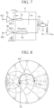
- the output load (output reflection coefficient) of the second amplifier 8b that operates as the main amplifier at the time of the backoff operation when a 4.2 GHz input signal is inputted to the input terminal 1 is considered using FIGS. 7 and 8 .
- the optimal load of each of the first and second amplifiers 8a and 8b at the time of the saturation power, and the characteristic impedance of each of the first and second output circuits 9a and 9b are assumed to be R opt which is the same as that in the case where a 1.6 GHz input signal is inputted to the input terminal 1.
- the second amplifier 8b operates as the auxiliary amplifier, the second amplifier 8b is placed in the off state, more specifically, at rest and the output end 8a2 of the second amplifier 8b is open at the time of the backoff operation.
- the output load ⁇ 4 at the output combination point 9A is 0.5 ⁇ R opt .
- the output load ⁇ 6 in the first amplifier 8a increases from the output load ⁇ 4 shown by a curve S2 to 2 ⁇ R opt or more because of both the enlargement of the output reflection coefficient ⁇ 5 which depends on the reactiveness of the second output circuit 9b, and the load modulation by the first output circuit 9a shown by a curve M2.
- the output load is matched with R opt .
- the Doherty amplifier according to Embodiment 1 operates as the one in which when a 4.2 GHz input signal is inputted to the input terminal 1, because of the effect of the load modulation by the output combination circuit 9, the output load (output reflection coefficient) of the first amplifier 8a is increased to two or more times as large as the optimal load R opt at the time of the saturation power, and a high-efficiency load is achieved also at the time of the backoff operation when the output power is lower than the saturation power.
- each of the first and second amplifiers 8a and 8b is switched between the one as the main amplifier and the one as the auxiliary amplifier in accordance with the amplitudes of the input signals inputted to the first and second amplifiers 8a and 8b in the state in which the gate bias voltage of each of the first and second amplifiers 8a and 8b is fixed to the one at which they operate as a class B amplifier, as the functions of the first and second amplifiers 8a and 8b when an input signal lying in the first frequency band is inputted and when an input signal lying in the second frequency band is inputted are schematically shown in FIG. 9 .
- the Doherty amplifier according to Embodiment 1 operates in multiple frequency bands which are an input signal lying in the first frequency band and an input signal lying in the second frequency band, without requiring the control of the gate bias voltage in the first amplifier 8a and the gate bias voltage in the second amplifier 8b.
- the Doherty amplifier according to Embodiment 1 operates as the one in which a high-efficiency load is achieved also at the time of the backoff operation when the output power is lower than the saturation power.
- the Doherty amplifier according to Embodiment 1 provides comparable drain efficiencies with respect to the output power when a 1.6 GHz input signal lying in the first frequency band is inputted to the input terminal 1 and when a 4.2 GHz input signal lying in the second frequency band is inputted to the input terminal 1, as shown in FIG. 10 .
- a Doherty amplifier according to Embodiment 2 will be explained on the basis of FIGS. 11 to 13 .
- the Doherty amplifier according to Embodiment 1 amplifies an input signal lying in the first frequency band and an input signal lying in the second frequency band
- the Doherty amplifier according to Embodiment 2 further amplifies an input signal in a third frequency band which is a frequency range different from the first and second frequency bands.
- the third frequency band is a frequency range higher than the second frequency band.
- Input signals inputted to two parallel amplifiers which constitute the Doherty amplifier satisfy a relation showing that when a second frequency lying in the second frequency band is assumed to be 1.0, a first frequency lying in the first frequency band is 0.5 with respect to the second frequency, and a third frequency lying in the third frequency band is 1.5 with respect to the second frequency.
- the Doherty amplifier according to Embodiment 2 differs from the Doherty amplifier according to Embodiment 1 in a first filter circuit 61a and a second filter circuit 61b, and a output combination circuit 91 comprised of a first output circuit 91a and a second output circuit 91b, and the other components are the same as those of the Doherty amplifier according to Embodiment 1.
- the first filter circuit 6a When an input signal lying in the first frequency band is inputted, the first filter circuit 6a outputs a first input signal obtained by attenuating the input signal lying in the first frequency band by a first amount of attenuation XdB, when an input signal lying in the second frequency band is inputted, the first filter circuit 6a outputs a second input signal obtained by allowing passage of the input signal lying in the second frequency band, and when an input signal lying in the third frequency band is inputted, the first filter circuit 6a outputs a fifth input signal obtained by attenuating the input signal lying in the third frequency band by a fourth amount of attenuation.
- the fourth amount of attenuation is XdB which is the same as the first amount of attenuation. More specifically, when an input signal lying in the third frequency band is inputted, the first filter circuit 6a outputs a fifth input signal obtained by attenuating the input signal lying in the third frequency band by Xdb.
- the first filter circuit 61a When the input signal lies in the first frequency band, the first filter circuit 61a outputs a signal having a small amplitude because the first input signal is attenuated by XdB, when the input signal lies in the second frequency band, the first filter circuit 61a outputs a signal having a large amplitude because the second input signal is not attenuated, and when the input signal lies in the third frequency band, the first filter circuit 61a outputs a signal having a small amplitude because the third input signal is attenuated by XdB.
- the first filter circuit 61a is a band pass filter circuit that when the input signal lies in the first frequency band and the third frequency band, attenuates the input signal, and when the input signal lies in the second frequency band, allows passage of the input signal.
- the first filter circuit 61a is a reactive band pass filter circuit which is comprised of a reactive reflection loss, such as a filter circuit using a lumped constant element, a filter circuit using a distributed constant line, a filter circuit which is a combination of a lumped constant and a distributed constant, or a filter circuit using an LC matching circuit.
- a reactive reflection loss such as a filter circuit using a lumped constant element, a filter circuit using a distributed constant line, a filter circuit which is a combination of a lumped constant and a distributed constant, or a filter circuit using an LC matching circuit.
- the downsizing of the first filter circuit 61a can be achieved.
- a resistive band pass filter circuit such as an attenuator, instead of a reactive band pass filter circuit, may be used.
- the first filter circuit 61a a filter bank whose path for the input signal differs in accordance with the first through third frequency bands, instead of a band pass filter circuit, may be used.
- the second filter circuit 61b When an input signal lying in the first frequency band is inputted, the second filter circuit 61b outputs a third input signal obtained by allowing passage of the input signal lying in the first frequency band, when an input signal lying in the second frequency band is inputted, the second filter circuit 61b outputs a fourth input signal obtained by attenuating the input signal lying in the second frequency band by the first amount of attenuation XdB, and when an input signal lying in the third frequency band is inputted, the second filter circuit 61b outputs a sixth input signal obtained by attenuating the input signal lying in the third frequency band by a fifth amount of attenuation smaller than the fourth amount of attenuation.
- the fifth amount of attenuation is 0dB. More specifically, when an input signal lying in the third frequency band is inputted, the second filter circuit 61b outputs a sixth input signal obtained by allowing passage of the input signal lying in the third frequency band.
- the second filter circuit 61b When the input signal lies in the first frequency band, the second filter circuit 61b outputs a signal having a large amplitude because the third input signal is not attenuated, when the input signal lies in the second frequency band, the second filter circuit 61b outputs a signal having a small amplitude because the fourth input signal is attenuated by XdB, and when the input signal lies in the third frequency band, the second filter circuit 61b outputs a signal having a large amplitude because the sixth input signal is not attenuated.
- the second filter circuit 61b is a band stop filter circuit that when the input signal lies in the first frequency band and the third frequency band, allows passage of the input signal, and when the input signal lies in the second frequency band, attenuates the input signal.
- the second filter circuit 61b is a reactive band stop filter circuit which is comprised of a reactive reflection loss, such as a filter circuit using a lumped constant element, a filter circuit using a distributed constant line, a filter circuit which is a combination of a lumped constant and a distributed constant, or a filter circuit using an LC matching circuit.
- a reactive reflection loss such as a filter circuit using a lumped constant element, a filter circuit using a distributed constant line, a filter circuit which is a combination of a lumped constant and a distributed constant, or a filter circuit using an LC matching circuit.
- the downsizing of the second filter circuit 61b can be achieved.
- a resistive band stop filter circuit such as an attenuator, instead of a reactive band stop filter circuit, may be used.
- a filter bank whose path for the input signal differs in accordance with the first through third frequency bands instead of a band stop filter circuit, may be used.
- the amount of attenuation XdB in the first filter circuit 6a with respect to the third frequency band is set to 6dB, as an example, when it is desirable to improve the efficiency of the second amplifier 8b, or is set to 3dB, as an example, when it is desirable to balance the efficiency and linearity of the second amplifier 8b.
- Each of the first and second amplifiers 8a and 8b is biased to a threshold voltage at which each of the amplifiers operates as a class B amplifier, i.e., the threshold voltage of a transistor which constitutes each of the first and second amplifiers 8a and 8b.
- the first amplifier 8a has an input end 8a1 connected to a gate bias terminal 11a at which a gate bias voltage is fixed, and when the first input signal outputted from the first filter circuit 61a is inputted to the input end 8a1 via a first input matching circuit 7a, the first amplifier 8a starts at a time later than the second amplifier 8b and operates as an auxiliary amplifier because the amplitude of the first input signal is smaller than the amplitude of the third input signal, when the second input signal outputted from the first filter circuit 61a is inputted to the input end 8a1, the first amplifier 8a starts at a time earlier than the second amplifier 8b and operates as a main amplifier because the amplitude of the second input signal is larger than the amplitude of the fourth input signal, and when the fifth input signal outputted from the first filter circuit 61a is inputted to the input end 8a1, the first amplifier 8a starts at a time later than the second amplifier 8b and operates as the auxiliary amplifier because the amplitude of the fifth input signal is smaller than the amplitude of
- the first amplifier 8a when the input signal inputted to the input terminal 1 lies in the first frequency band, the first amplifier 8a operates as the auxiliary amplifier, when the input signal inputted to the input terminal 1 lies in the second frequency band, the first amplifier 8a operates as the main amplifier, and when the input signal inputted to the input terminal 1 lies in the first frequency band, the first amplifier 8a operates as the auxiliary amplifier.
- the saturation output power when operating as the main amplifier and the saturation output power when operating as the auxiliary amplifier are equal.
- the second amplifier 8b has an input end 8b1 connected to a gate bias terminal 11b at which a gate bias voltage is fixed, and when the third input signal outputted from the second filter circuit 6b is inputted to the input end 8b1 via a second input matching circuit 7b, the second amplifier 8b starts at a time earlier than the first amplifier 8a and operates as the main amplifier because the amplitude of the third input signal is larger than the amplitude of the first input signal, when the fourth input signal outputted from the second filter circuit 6b is inputted to the input end 8b1, the second amplifier 8b starts at a time later than the second amplifier 8b and operates as the auxiliary amplifier because the amplitude of the fourth input signal is smaller than the amplitude of the second input signal, and when the sixth input signal outputted from the second filter circuit 6b is inputted to the input end 8b1, the second amplifier 8b starts at a time earlier than the first amplifier 8a and operates as the main amplifier because the amplitude of the sixth input signal is larger than the amplitude of the fifth input signal.
- the second amplifier 8b when the input signal inputted to the input terminal 1 lies in the first frequency band, the second amplifier 8b operates as the main amplifier, when the input signal inputted to the input terminal 1 lies in the second frequency band, the second amplifier 8b operates as the auxiliary amplifier, and when the input signal inputted to the input terminal 1 lies in the third frequency band, the second amplifier 8b operates as the main amplifier.
- the saturation output power when operating as the main amplifier and the saturation output power when operating as the auxiliary amplifier are equal.
- the times that the first amplifier 8a and the second amplifier 8b start differ because the amplitudes of the input signals inputted to the first amplifier 8a and the second amplifier 8b differ because of the first filter circuit 6a and the second filter circuit 6b, as explained in the Doherty amplifier according to Embodiment 1.
- the output load impedances of the first amplifier 8a and the second amplifier 8b differ.
- the first amplifier 8a and the second amplifier 8b operate in the same way that those of the Doherty amplifier according to Embodiment 1 operate.
- the time that the second amplifier 8b starts is earlier than the time that the first amplifier 8a starts, and the second amplifier 8b functions as the main amplifier while the first amplifier 8a functions as the auxiliary amplifier.
- the output load impedance of the first amplifier 8a is sufficiently higher than that of the second amplifier 8b, for example, the output load impedance of the first amplifier 8a is ten or more times as high as that of the second amplifier 8b, and it can be assumed from the viewpoint of the load modulation of the Doherty amplifier that the first amplifier 8a is placed in an off state and the output of the first amplifier 8a is open.
- the second amplifier 8b operates with a high degree of efficiency even at the time of low power output.
- the first output circuit 91a is a transmission line having an electric length which is less than 90 degrees with respect to the first frequency band, which is equal to 90 degrees with respect to the second frequency band, and which is greater than or equal to 90 degrees with respect to the third frequency band, and its characteristic impedance is equal to an optimum load impedance at the time of the saturation power of the first amplifier 8a.
- the first output circuit 9a is not limited to the transmission line, and should just satisfy the above-mentioned requirements.
- the electric length value which is less than 90 degrees with respect to the first frequency band ranges from less than 90 degrees to 45 degrees, for example.
- the electric length value which is equal to 90 degrees with respect to the second frequency band contains 90 degrees itself and even a plus or minus design tolerance value with respect to the value of 90 degrees at which the load modulation making it possible to expect that the first amplifier 8a operates with the highest degree of efficiency in the second frequency band is established.
- the electric length value which is greater than or equal to 90 degrees with respect to the third frequency band ranges up to 135 degrees, for example.
- the second output circuit 9b is a transmission line having an electric length which is greater than 90 degrees with respect to the first frequency band, which is equal to 180 degrees with respect to the second frequency band, and which is less than 270 degrees with respect to the third frequency band, and its characteristic impedance is equal to an optimum load impedance at the time of the saturation power of the second amplifier 8b.
- the second output circuit 9b is not limited to the transmission line, and should just satisfy the above-mentioned requirements.
- the electric length value which is greater than 90 degrees with respect to the first frequency band ranges from more than 90 degrees to (90+16) degrees, for example.
- the electric length value which is equal to 180 degrees with respect to the second frequency band contains 180 degrees itself and even a plus or minus design tolerance value with respect to the value of 180 degrees at which the second amplifier 8b is placed in an off state in the second frequency band, the open load of the output end 8b2 is propagated, and the output end of the second output circuit 91b is open.
- the electric length value which is less than 270 degrees with respect to the third frequency band ranges from less than 270 degrees to (270-16) degrees, for example.
- the output combination circuit 91 which is comprised of the first output circuit 91a and the second output circuit 91b should just have the characteristic of, at the time of the backoff operation, enlarging the output load (output reflection coefficient) of the main amplifier when the first amplifier 8a or the second amplifier 8b functions as the main amplifier in accordance with the frequency.
- the first output circuit 91a and the second output circuit 91b should just be configured in such a way as to have the characteristic of enlarging the output load (output reflection coefficient) of the first amplifier 8a in accordance with the frequency of the input signal because the first amplifier 8a functions as the main amplifier when the frequency band of the input signal is the second frequency band, and enlarging the output load (output reflection coefficient) of the second amplifier 8b in accordance with the frequency of the input signal because the second amplifier 8b functions as the main amplifier when the frequency band of the input signal is the first frequency band and the third frequency band.
- the Doherty amplifier When an input signal of the first frequency lying in the first frequency band, concretely, 1.6 GHz is inputted to the input terminal 1 and when an input signal of the second frequency lying in the second frequency band, concretely, 4.2 GHz is inputted to the input terminal 1, the Doherty amplifier operates in the same way that the Doherty amplifier according to Embodiment 1 operates.
- An input signal of the third frequency lying in the third frequency band is inputted to a splitter 4 via a third input matching circuit 3, and the splitter 4 splits the input signal inputted thereto to an input signal at an output end thereof and an input signal at another output end thereof.
- the input signal outputted from the output end of the splitter 4 undergoes a phase correction in a phase correction circuit 5 and is then inputted to the first filter circuit 61a, and the first filter circuit 61a filters the input signal inputted thereto and outputs a fifth input signal.
- the filtering by the first filter circuit 61a provides a fifth input signal obtained by attenuating the input signal by XdB because the input signal lies in the third frequency band.
- the fifth input signal is inputted to the input end 8a1 of the first amplifier 8a via the first input matching circuit 7a.
- the input signal outputted from the other output end of the splitter 4 is inputted to the second filter circuit 61b.
- the second filter circuit 61b outputs a sixth input signal obtained by allowing passage of the input signal without attenuating the input signal.
- the sixth input signal is inputted to the input end 8b1 of the second amplifier 8b via the second input matching circuit 7b.
- the amplitude of the sixth input signal is larger than that of the fifth input signal because the fifth input signal is attenuated by XdB by the first filter circuit 6a.
- the second amplifier 8b starts at an earlier time and the first amplifier 8a starts at a later time.
- the second amplifier 8b operates as the main amplifier while the first amplifier 8a operates as the auxiliary amplifier.
- the Doherty amplifier according to Embodiment 2 When an input signal of the third frequency lying in the third frequency band is inputted to the input terminal 1, the Doherty amplifier according to Embodiment 2 operates as the one in which the second amplifier 8b operates as the main amplifier while the first amplifier 8a operates as the auxiliary amplifier, and outputs the input signal of the third frequency inputted to the input terminal 1 from an output terminal 2 after amplifying the input signal.
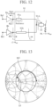
- the output load (output reflection coefficient) of the second amplifier 8b that operates as the main amplifier at the time of the backoff operation when a third input signal is inputted to the input terminal 1 is considered using FIGS. 12 and 13 .
- R opt which is the same as that in the case where input signals of the first frequency and the second frequency is inputted to the input terminal 1.
- the first amplifier 8a operates as the auxiliary amplifier, the first amplifier 8a is placed in the off state, more specifically, at rest and the output end 8a2 of the first amplifier 8a is open at the time of the backoff operation.
- the output load ⁇ 7 at the output combination point 91A is 0.5 ⁇ R opt .
- the output load ⁇ 9 in the second amplifier 8b increases from the output load ⁇ 7 shown by a curve S3 to 2 ⁇ R opt or more because of both the enlargement of the output reflection coefficient ⁇ 8 which depends on the reactiveness of the second output circuit 9b, and the load modulation by the first output circuit 9a shown by a curve M3.
- the output load is matched with R opt .
- the Doherty amplifier according to Embodiment 2 operates as the one in which when a third input signal is inputted to the input terminal 1, because of the effect of the load modulation by the output combination circuit 9, the output load (output reflection coefficient) of the second amplifier 8b is increased to two or more times as large as the optimal load R opt at the time of the saturation power, and a high-efficiency load is achieved also at the time of the backoff operation when the output power is lower than the saturation power.
- each of the first and second amplifiers 8a and 8b is switched between the one as the main amplifier and the one as the auxiliary amplifier in accordance with the amplitudes of the input signals inputted to the first and second amplifiers 8a and 8b in a state in which the gate bias voltage of each of the first and second amplifiers 8a and 8b is fixed to the one at which they operate as a class B amplifier.
- the Doherty amplifier according to Embodiment 2 operates in multiple frequency bands which are an input signal lying in the first frequency band, an input signal lying in the second frequency band, and an input signal lying in the third frequency band without requiring the control of the gate bias voltage in the first amplifier 8a and the gate bias voltage in the second amplifier 8b.
- the Doherty amplifier according to Embodiment 2 operates as the one in which, also when an input signal lying in the third frequency band is inputted, a high-efficiency load is achieved also at the time of the backoff operation when the output power is lower than the saturation power because of the effect of the load modulation of the output combination circuit 9.
- the Doherty amplifier according to Embodiment 1 is aimed at amplifying an input signal lying in the first frequency band and an input signal lying in the second frequency band
- the Doherty amplifier according to Embodiment 2 is aimed at amplifying an input signal lying in one of the first through third frequency bands
- a Doherty amplifier further aimed at signals lying in a fourth frequency band, in a fifth frequency band, and in higher frequency bands.
- the output circuit of the main amplifier when the first amplifier 8a or the second amplifier 8b functions as the main amplifier in accordance with a higher frequency is set up in such a way that a relation of (90 degrees + 180 degrees ⁇ n) (n is a natural number) holds.
- first filter circuit 6a and the second filter circuit 6b are comprised of filter banks.
- the Doherty amplifier according to the present disclosure is suitable for amplifiers, such as amplifiers used for mobile communication base stations, which amplify a signal for communications with a high degree of efficiency.
Landscapes
- Engineering & Computer Science (AREA)
- Power Engineering (AREA)
- Amplifiers (AREA)
Abstract
Description
- The present disclosure relates to a Doherty amplifier that operates in multiple frequency bands.
- In recent years, because of a dramatic increase in communications traffic, it is required that, for example, amplifiers for 5th-generation mobile communication base stations can amplify a signal with a large peak to average power ratio (PAPR) with a high degree of efficiency.
- As an amplifier that amplifies a signal for communications with a high degree of efficiency, a Doherty amplifier is proposed in
Patent Literature 1. - The Doherty amplifier shown in
Patent Literature 1 is one in which a control unit switches the class of operation for each of first and second amplifying elements in accordance with whether the operating frequency of an input signal is a first operating frequency or a second operating frequency. - Patent Literature 1:
WO 2019/09760 - On the other hand, it is desired that a Doherty amplifier that amplifies input signals of two operating frequencies without controlling the two amplifying elements that constitute the Doherty amplifier is implemented.
- The present disclosure is provided in view of the above-mentioned point, and it is an object of the present disclosure to provide a Doherty amplifier that operates in multiple frequency bands without having to control the amplifying elements which constitute the Doherty amplifier.
- A Doherty amplifier according to the present disclosure includes: a first filter circuit to, when an input signal lying in a first frequency band is inputted, output a first input signal obtained by attenuating the input signal lying in the first frequency band by a first amount of attenuation, and to, when an input signal lying in a second frequency band different from the first frequency band is inputted, output a second input signal obtained by allowing passage of the input signal lying in the second frequency band; a second filter circuit to, when an input signal lying in the first frequency band is inputted, output a third input signal obtained by attenuating the input signal lying in the first frequency band by a second amount of attenuation smaller than the first amount of attenuation, and to, when an input signal lying in the second frequency band is inputted, output a fourth input signal obtained by attenuating the input signal lying in the second frequency band by a third amount of attenuation larger than or equal to the first amount of attenuation; a first amplifier in which a gate bias voltage is fixed, to operate as an auxiliary amplifier when the first input signal from the first filter circuit is inputted, and to operate as a main amplifier when the second input signal from the first filter circuit is inputted; and a second amplifier in which a gate bias voltage is fixed, to operate as the main amplifier when the third input signal from the second filter circuit is inputted, and to operate as the auxiliary amplifier when the fourth input signal from the second filter circuit is inputted.
- According to the present disclosure, because the first filter circuit and the second filter circuit which have different characteristics are disposed as stages preceding the first amplifier and the second amplifier, the Doherty amplifier operates in the multiple frequency bands without having to control the first amplifier and the second amplifier.
-
-
FIG. 1 is a block diagram showing a Doherty amplifier according to Embodiment 1. -
FIG. 2 is an equivalent circuit diagram showing a first amplifier in the Doherty amplifier according toEmbodiment 1. -
FIG. 3 is an equivalent circuit diagram showing a second amplifier in the Doherty amplifier according toEmbodiment 1. -
FIG. 4 is a view showing a pass loss with respect to frequencies in a first filter circuit and a second filter circuit in the Doherty amplifier according toEmbodiment 1. -
FIG. 5 is an equivalent circuit diagram showing the first amplifier, the second amplifier, and an output combining circuit, in order to show a relation among impedances at the time of backoff when an input signal having a first frequency (lying in a low frequency region) is inputted in the Doherty amplifier inEmbodiment 1. -
FIG. 6 is a view showing an impedance transformation in a Smith chart at the time of backoff when an input signal having the first frequency (lying in the low frequency region) is inputted in the Doherty amplifier inEmbodiment 1. -
FIG. 7 is an equivalent circuit diagram showing the first amplifier, the second amplifier, and the output combining circuit, in order to show a relation among impedances at the time of backoff when an input signal having a second frequency (lying in a high frequency region) is inputted in the Doherty amplifier inEmbodiment 1. -
FIG. 8 is a view showing an impedance transformation in a Smith chart at the time of backoff when an input signal having the second frequency (lying in the low frequency region) is inputted in the Doherty amplifier inEmbodiment 1. -
FIG. 9 is a view schematically showing the functions of the first amplifier and the second amplifier when an input signal lying in a first frequency band is inputted and when an input signal lying in a second frequency band is inputted in the Doherty amplifier according toEmbodiment 1. -
FIG. 10 is a view showing a drain efficiency with respect to output power, the drain efficiency being a simulation result, in the Doherty amplifier according toEmbodiment 1. -
FIG. 11 is a block diagram showing a Doherty amplifier according to Embodiment 2. -
FIG. 12 is an equivalent circuit diagram showing a first amplifier, a second amplifier, and an output combining circuit, in order to show a relation among impedances at the time of backoff when an input signal having a third frequency is inputted in the Doherty amplifier inEmbodiment 2. -
FIG. 13 is a view showing an impedance transformation in a Smith chart at the time of backoff when an input signal having the third frequency is inputted in the Doherty amplifier inEmbodiment 2. - A Doherty amplifier according to Embodiment 1 will be explained on the basis of
FIGS. 1 to 10 . - The Doherty amplifier operates in two operating frequency bands: a first frequency band and a second frequency band.
- The first frequency band and the second frequency band are different frequency ranges, and the first frequency band is a frequency range lower than the second frequency band. For the sake of convenience, the first frequency band is referred to as a low frequency range showing a frequency range lower than the second frequency band, and the second frequency band is referred to as a high frequency range showing a frequency range higher than the first frequency band.
- In the Doherty amplifier, a gate bias voltage applied to each of two amplifiers in parallel is fixed to one at which each of the amplifiers operates as a class B amplifier, and two filter circuits connected as stages preceding the two parallel amplifiers cause each of the two parallel amplifiers to switch between a main amplifier function and an auxiliary amplifier function according to the two operating frequency bands in which the pass losses in these operating frequency bands are made to differ from each other.
- In the two parallel amplifiers, two amplifiers: main and auxiliary amplifiers with equal saturation output power are connected in parallel.
- Input signals inputted to the two parallel amplifiers satisfy a relation showing that when a second frequency in the second frequency band is assumed to be 1.0, a first frequency in the first frequency band is 0.5 with respect to the second frequency.
- The Doherty amplifier includes, between an
input terminal 1 and anoutput terminal 2, a thirdinput matching circuit 3, asplitter 4, a phase correction circuit 5, afirst filter circuit 6a, asecond filter circuit 6b, a firstinput matching circuit 7a, a secondinput matching circuit 7b, the twoparallel amplifiers 8 having afirst amplifier 8a and asecond amplifier 8b, anoutput combination circuit 9 having afirst output circuit 9a and asecond output circuit 9b, and anoutput matching circuit 10. - The third
input matching circuit 3 is connected between theinput terminal 1 and an input end of thesplitter 4, and performs impedance matching between theinput terminal 1 and thesplitter 4. - The third
input matching circuit 3 is an impedance matching network (IMN) that includes a matching circuit using a lumped constant element, a matching circuit using a distributed constant line, a matching circuit which is a combination of a lumped constant and a distributed constant, a matching circuit using an LC matching circuit, or the like. - The
splitter 4 has an input end connected to an output end of the thirdinput matching circuit 3, an output end connected to an input end of the phase correction circuit 5, and another output end connected to thesecond filter circuit 6b, and splits an input signal inputted thereto from theinput terminal 1 to an input signal at the output end thereof and an input signal at the other output end thereof. - The
splitter 4 is a Wilkinson splitter, a hybrid circuit, or the like which is comprised of a circuit using a lumped constant element, a circuit using a distributed constant line, a circuit which is a combination of a lumped constant and a distributed constant, a circuit using an LC matching circuit, or the like. - The phase correction circuit 5 is connected between the output end of the
splitter 4 and an input end of thefirst filter circuit 6a, and causes the electric length from the output end of thesplitter 4 to anoutput combination point 9A which is an output end of theoutput combination circuit 9, i.e., the electric length of a path on a side of thefirst amplifier 8a to be equal to the electric length from the other output end of thesplitter 4 to theoutput combination point 9A of theoutput combination circuit 9, i.e., the electric length of a path on a side of thesecond amplifier 8b. - The phase correction circuit 5 is comprised of a circuit using a lumped constant element, a circuit using a distributed constant line, a circuit which is a combination of a lumped constant and a distributed constant, a circuit using an LC matching circuit, or the like.
- The input end of the
first filter circuit 6a is connected to an output end of the phase correction circuit 5, and thefirst filter circuit 6a receives the input signal outputted from the output end of thesplitter 4 and inputted thereto via the phase correction circuit 5. - When an input signal lying in the first frequency band is inputted, the
first filter circuit 6a outputs a first input signal obtained by attenuating the input signal lying in the first frequency band by a first amount of attenuation XdB, and when an input signal lying in the second frequency band is inputted, thefirst filter circuit 6a outputs a second input signal obtained by allowing passage of the input signal lying in the second frequency band. - When the input signal lies in the first frequency band, the
first filter circuit 6a outputs a signal having a small amplitude because the first input signal is attenuated by XdB, and when the input signal lies in the second frequency band, thefirst filter circuit 6a outputs a signal having a large amplitude because the second input signal is not attenuated. - The above-mentioned amplitude of the input signal refers to the amplitude of the envelope of the signal. The amplitude of an input signal, which will be explained below, also refers to the amplitude of the envelope of the signal.
- The
first filter circuit 6a is a high pass filter circuit in which the amount of attenuation in the first frequency band is set to XdB, and the amount of attenuation in the second frequency band is set to 0dB (passage), as shown by a solid line A inFIG. 4 . - The
first filter circuit 6a is a reactive high pass filter circuit comprised of a reactive reflection loss, such as a filter circuit using a lumped constant element, a filter circuit using a distributed constant line, a filter circuit which is a combination of a lumped constant and a distributed constant, or a filter circuit using an LC matching circuit. - In a case where a reactive high pass filter circuit is used as the
first filter circuit 6a, the downsizing of thefirst filter circuit 6a can be achieved. - As the
first filter circuit 6a, a resistive high pass filter circuit such as an attenuator, instead of a reactive high pass filter circuit, may be used. - In a case where a resistive high pass filter circuit is used as the
first filter circuit 6a, operational stability can be provided for thefirst amplifier 8a because the reflection power is lost in thefirst filter circuit 6a. - The
second filter circuit 6b has an input end connected to the other output end of thesplitter 4, and receives the input signal outputted from the other output end of thesplitter 4 and inputted thereto. - When an input signal lying in the first frequency band is inputted, the
second filter circuit 6b outputs a third input signal obtained by allowing passage of the input signal lying in the first frequency band, and when an input signal lying in the second frequency band is inputted, thesecond filter circuit 6b outputs a fourth input signal obtained by attenuating the input signal lying in the second frequency band by the first amount of attenuation XdB. - When the input signal lies in the first frequency band, the
second filter circuit 6b outputs a signal having a large amplitude because the third input signal is not attenuated, and when the input signal lies in the second frequency band, thesecond filter circuit 6b outputs a signal having a small amplitude because the fourth input signal is attenuated by XdB. - The
second filter circuit 6b is a low pass filter circuit in which the amount of attenuation in the first frequency band is set to 0dB (passage), and the amount of attenuation in the second frequency band is set to XdB, as shown by a solid line B inFIG. 4 . - The
second filter circuit 6b is a reactive low pass filter circuit comprised of a reactive reflection loss, such as a filter circuit using a lumped constant element, a filter circuit using a distributed constant line, a filter circuit which is a combination of a lumped constant and a distributed constant, or a filter circuit using an LC matching circuit. - In a case where a reactive high pass filter circuit is used as the
second filter circuit 6b, the downsizing of thesecond filter circuit 6b can be achieved. - As the
second filter circuit 6b, a resistive low pass filter circuit such as an attenuator, instead of a reactive low pass filter circuit, may be used. - In a case where a resistive high pass filter circuit is used as the
second filter circuit 6b, operational stability can be provided for thesecond amplifier 8b because the reflection power is lost in thesecond filter circuit 6b. - Although when the input signal lies in the first frequency band, the
second filter circuit 6b outputs, as the third input signal, the signal which the second filter circuit does not attenuate (the amount of attenuation is 0dB: passage), thesecond filter circuit 6b may output, as the third input signal, the signal which the second filter circuit attenuates by a second amount of attenuation smaller than the first amount of attenuation XdB. - Further, although when the input signal lies in the second frequency band, the
second filter circuit 6b outputs, as the fourth input signal, the signal which the second filter circuit attenuates by the first amount of attenuation XdB, thesecond filter circuit 6b may output, as the fourth input signal, the signal which the second filter circuit attenuates by a third amount of attenuation larger than or equal to the first amount of attenuation XdB. - To sum up, what is necessary is just to set up the characteristics of the
first filter circuit 6a and thesecond filter circuit 6b in such a way that when the input signal lies in the first frequency band, the amplitude of the first input signal outputted from thefirst filter circuit 6a is smaller than the amplitude of the third input signal outputted from thesecond filter circuit 6b, whereas when the input signal lies in the second frequency band, the amplitude of the second input signal outputted from thefirst filter circuit 6a is larger than the amplitude of the fourth input signal outputted from thesecond filter circuit 6b. - The amount of attenuation XdB in the
first filter circuit 6a with respect to the first frequency band and the amount of attenuation XdB in thesecond filter circuit 6b with respect to the second frequency band are set to 6dB, as an example, when it is desirable to improve the efficiency of each of the first andsecond amplifiers second amplifiers - The first
input matching circuit 7a is an impedance matching network (IMN) which is connected between an output end of thefirst filter circuit 6a and an input end 8a1 of thefirst amplifier 8a, and which performs input matching with thefirst amplifier 8a. - The first
input matching circuit 7a is an impedance matching network (IMN) which is comprised of a matching circuit using a lumped constant element, a matching circuit using a distributed constant line, a matching circuit which is a combination of a lumped constant and a distributed constant, a matching circuit using an LC matching circuit, or the like. - The first
input matching circuit 7a may be connected between the output end of the phase correction circuit 5 and the input end of thefirst filter circuit 6a. - The second
input matching circuit 7b is an impedance matching network (IMN) which is connected between an output end of thesecond filter circuit 6b and aninput end 8bsecond amplifier 8b, and which performs input matching with thesecond amplifier 8b. - The second
input matching circuit 7b is an impedance matching network (IMN) which is comprised of a matching circuit using a lumped constant element, a matching circuit using a distributed constant line, a matching circuit which is a combination of a lumped constant and a distributed constant, a matching circuit using an LC matching circuit, or the like. - The second
input matching circuit 7b may be connected between the other output end of thesplitter 4 and the input end of thesecond filter circuit 6b. - The two
parallel amplifiers 8 is comprised of thefirst amplifier 8a and thesecond amplifier 8b, and each of the first andsecond amplifiers second amplifiers - The threshold voltage in the present disclosure contains the value of the threshold voltage itself and even a plus or minus design tolerance value with respect to the value of the threshold voltage.
- The input end 8a1 of the
first amplifier 8a is connected to agate bias terminal 11a at which the gate bias voltage is fixed, and when the first input signal outputted from thefirst filter circuit 6a is inputted to the input end 8a1 via the firstinput matching circuit 7a, thefirst amplifier 8a starts at a time later than thesecond amplifier 8b and operates as the auxiliary amplifier because the amplitude of the first input signal is smaller than the amplitude of the third input signal, whereas when the second input signal outputted from thefirst filter circuit 6a is inputted to the input end 8a1, thefirst amplifier 8a starts at a time earlier than thesecond amplifier 8b and operates as the main amplifier because the amplitude of the second input signal is larger than the amplitude of the fourth input signal. - More specifically, the
first amplifier 8a operates as the auxiliary amplifier when the input signal inputted to theinput terminal 1 lies in the first frequency band, whereas thefirst amplifier 8a operates as the main amplifier when the input signal inputted to theinput terminal 1 lies in the second frequency band. - In the
first amplifier 8a, the saturation output power when operating as the main amplifier and the saturation output power when operating as the auxiliary amplifier are equal. - As the
first amplifier 8a, a transistor such as a field effect transistor (FET), a heterojunction bipolar transistor (HBT), or a high electron mobility transistor (HEMT) is used. - The
first amplifier 8a may include circuit configuration elements needed as the amplifier, such as a stabilization circuit connected to an input side of the transistor and a bias circuit connected to an output side of the transistor. - The transistor as the
first amplifier 8a has a gate electrode serving as the input end 8a1, a drain electrode serving as an output end 8a2 and connected, via a load resistor, to a power supply potential Vcc, and a source electrode connected to a ground node. - The input end 8a1 is connected to the
gate bias terminal 11a, and thegate bias terminal 11a is connected to the power supply potential Vcc via a resistive element (bias resister). - To the
gate bias terminal 1 1a is applied the threshold voltage of the transistor in such a way that the transistor as thefirst amplifier 8a operates as a class B amplifier. - An equivalent circuit of the
first amplifier 8a is shown inFIG. 2 . More specifically, it is assumed that thefirst amplifier 8a is comprised of a current source Ia which is based on a current flowing between the drain and the source of the transistor, and an output capacitance Ca which is a parasitic capacitance between the drain of the transistor and the ground. - The output capacitance Ca of the
first amplifier 8a is compensated for by an inductor or the like or incorporated as a part of thefirst output circuit 9a, and the current source Ia is connected directly to thefirst output circuit 9a from the viewpoint of electric lengths. - The
input end 8bsecond amplifier 8b is connected to agate bias terminal 11b at which the gate bias voltage is fixed, and when the third input signal outputted from thesecond filter circuit 6b is inputted to theinput end 8binput matching circuit 7b, thesecond amplifier 8b starts at a time earlier than thefirst amplifier 8a and operates as the main amplifier because the amplitude of the third input signal is larger than the amplitude of the first input signal, whereas when the fourth input signal outputted from thesecond filter circuit 6b is inputted to theinput end 8bsecond amplifier 8b starts at a time later than thesecond amplifier 8b and operates as the auxiliary amplifier because the amplitude of the fourth input signal is smaller than the amplitude of the second input signal. - More specifically, the
second amplifier 8b operates as the main amplifier when the input signal inputted to theinput terminal 1 lies in the first frequency band, whereas thesecond amplifier 8b operates as the auxiliary amplifier when the input signal inputted to theinput terminal 1 lies in the second frequency band. - In the
second amplifier 8b, the saturation output power when operating as the main amplifier and the saturation output power when operating as the auxiliary amplifier are equal. - As the
second amplifier 8b, a transistor such as an FET, an HBT, or a HEMT is used. - The
second amplifier 8b may include circuit configuration elements needed as the amplifier, such as a stabilization circuit connected to an input side of the transistor and a bias circuit connected to an output side of the transistor. - The transistor as the
second amplifier 8b has a gate electrode serving as theinput end 8b - The input end 8b1 is connected to the
gate bias terminal 11b, and thegate bias terminal 11b is connected to the power supply potential Vcc via a resistive element (bias resister). - To the
gate bias terminal 11b is applied the threshold voltage of the transistor in such a way that the transistor as thefirst amplifier 8a operates as a class B amplifier. - The gate bias terminal 11b may also serve as the
gate bias terminal 11a. - An equivalent circuit of the
second amplifier 8b is shown inFIG. 3 . More specifically, it is assumed that thesecond amplifier 8b is comprised of: a current source Ib which is based on a current flowing between the drain and the source of the transistor; and an output capacitance Cb which is a parasitic capacitance between the drain of the transistor and the ground. - The output capacitance Cb of the
second amplifier 8b is compensated for by an inductor or the like or incorporated as a part of thesecond output circuit 9b, and the current source Ib is connected directly to thesecond output circuit 9b from the viewpoint of electric lengths. - To sum up, although the functions and configurations of the
first amplifier 8a and thesecond amplifier 8b are the same, the times that thefirst amplifier 8a and thesecond amplifier 8b start differ because the amplitudes of the input signals inputted to thefirst amplifier 8a and thesecond amplifier 8b differ because of thefirst filter circuit 6a and thesecond filter circuit 6b. - Because of the difference between the times that the
first amplifier 8a and thesecond amplifier 8b start, the output load impedances of thefirst amplifier 8a and thesecond amplifier 8b differ. - When the input signal lies in the first frequency band, the time that the
second amplifier 8b starts is earlier than the time that thefirst amplifier 8a starts, and thesecond amplifier 8b functions as the main amplifier while thefirst amplifier 8a functions as the auxiliary amplifier. - The output load impedance of the
first amplifier 8a is sufficiently higher than that of thesecond amplifier 8b, for example, the output load impedance of thefirst amplifier 8a is ten or more times as high as that of thesecond amplifier 8b, and it can be regarded from the viewpoint of the load modulation of the Doherty amplifier that thefirst amplifier 8a is placed in an off state and the output end 8a2 of thefirst amplifier 8a is open. - At this time, because an output circuit having an electric length close to 90 degrees is provided on an output side of the
second amplifier 8b because of thefirst output circuit 9a and thesecond output circuit 9b, and the output of thesecond amplifier 8b is in a load condition that a high degree of efficiency is achieved even at the time of low power output, thesecond amplifier 8b operates with a high degree of efficiency even at the time of low power output. - In contrast, when the input signal lies in the second frequency band, the time that the
first amplifier 8a starts is earlier than the time that thesecond amplifier 8b starts, and the output load impedance of thesecond amplifier 8b is sufficiently higher than that of thefirst amplifier 8a, for example, the output load impedance of thesecond amplifier 8b is ten or more times as high as that of thefirst amplifier 8a, and it can be assumed from the viewpoint of the load modulation of the Doherty amplifier that thesecond amplifier 8b is placed in an off state and the output end 8b2 of thesecond amplifier 8b is open. - As a result, the
first amplifier 8a functions as the main amplifier while thesecond amplifier 8b functions as the auxiliary amplifier. - At this time, because an output circuit having an electric length close to 90 degrees is provided on an output side of the
first amplifier 8a because of thefirst output circuit 9a and thesecond output circuit 9b, and the output of thefirst amplifier 8a is in a load condition that a high degree of efficiency is achieved even at the time of low power output, thefirst amplifier 8a operates with a high degree of efficiency even at the time of low power output. - The
output combination circuit 9 is comprised of thefirst output circuit 9a and thesecond output circuit 9b, and, at the time of a backoff operation, enlarges the output load (output reflection coefficient) of the main amplifier when thefirst amplifier 8a or thesecond amplifier 8b functions as the main amplifier in accordance with the frequency. - The
first output circuit 9a modulates the output load on thefirst amplifier 8a. - The
first output circuit 9a has an input end connected to the output end of thefirst amplifier 8a, and an output end connected to theoutput combination point 9A. - The
first output circuit 9a is a transmission line having an electric length which is less than 90 degrees with respect to the first frequency band, and which is equal to 90 degrees with respect to the second frequency band, and its characteristic impedance is equal to an optimum load impedance at the time of the saturation power of thefirst amplifier 8a. - The
first output circuit 9a is not limited to the transmission line, and should just satisfy the above-mentioned requirements. - In the
first output circuit 9a, the value which is less than 90 degrees with respect to the first frequency band ranges from less than 90 degrees to 45 degrees, for example. - Further, the value of the electric length which is equal to 90 degrees with respect to the second frequency band contains 90 degrees itself and even a plus or minus design tolerance value with respect to the value of 90 degrees at which the load modulation making it possible to expect that the
first amplifier 8a operates with the highest degree of efficiency in the second frequency band is established. - The
second output circuit 9b modulates the output load on thesecond amplifier 8b. - The
second output circuit 9b has an input end connected to the output end of thesecond amplifier 8b, and an output end connected to theoutput combination point 9A. - The
second output circuit 9b is a transmission line having an electric length which is greater than 90 degrees with respect to the first frequency band, and which is equal to 180 degrees with respect to the second frequency band, and its characteristic impedance is equal to an optimum load impedance at the time of the saturation power of thesecond amplifier 8b. - The
second output circuit 9b is not limited to the transmission line, and should just satisfy the above-mentioned requirements. - In the
second output circuit 9b, the value of the electric length which is greater than 90 degrees with respect to the first frequency band ranges from more than 90 degrees to (90+16) degrees, for example. - Further, the value of the electric length which is equal to 180 degrees with respect to the second frequency band contains 180 degrees itself and even a plus or minus design tolerance value with respect to the value of 180 degrees at which the
second amplifier 8b is placed in an off state in the second frequency band, the open load of the output end 8b2 is propagated, and the output end of thesecond output circuit 9b is open. - To sum up, the
output combination circuit 9 should just have the characteristic of, at the time of the backoff operation, enlarging the output load (output reflection coefficient) of the main amplifier when thefirst amplifier 8a or thesecond amplifier 8b functions as the main amplifier in accordance with the frequency. - More specifically, the
first output circuit 9a and thesecond output circuit 9b should just be configured in such a way as to have the characteristic of enlarging the output load (output reflection coefficient) of thefirst amplifier 8a in accordance with the frequency of the input signal because thefirst amplifier 8a functions as the main amplifier when the frequency band of the input signal is the second frequency band, and enlarging the output load (output reflection coefficient) of thesecond amplifier 8b in accordance with the frequency of the input signal because thesecond amplifier 8b functions as the main amplifier when the frequency band of the input signal is the first frequency band. - No isolation is provided between the output end 8a2 of the
first amplifier 8a and the output end 8b2 of thesecond amplifier 8b by thefirst output circuit 9a - theoutput combination point 9A - thesecond output circuit 9b. - When an input signal lying in the second frequency band is inputted to the
input terminal 1, thefirst amplifier 8a functions as the main amplifier in response to a second input signal lying in the second frequency band, and thesecond amplifier 8b functions as the auxiliary amplifier in response to a fourth input signal lying in the second frequency band, the transmission line of 90 degrees provided by thefirst output circuit 9a is connected to the output end 8a2 of thefirst amplifier 8a, and load modulation occurs in thefirst amplifier 8a, which functions as the main amplifier, more specifically, its apparent load impedance varies because of the transmission line of 180 degrees provided by thesecond output circuit 9b which is connected to the output end 8b2 of thesecond amplifier 8b. - As a result, when an input signal lying in the second frequency band is inputted to the
input terminal 1, the Doherty amplifier implements a high-efficiency operation at the backoff operating point where the output power is lower than the saturation power. - Further, when an input signal lying in the first frequency band is inputted to the
input terminal 1, thefirst amplifier 8a functions as the auxiliary amplifier in response to a first input signal lying in the first frequency band, and thesecond amplifier 8b functions as the main amplifier in response to a third input signal lying in the first frequency band, the transmission line of more than 90 degrees provided by thesecond output circuit 9b is connected to the output end 8b2 of thesecond amplifier 8b, and load modulation occurs in thesecond amplifier 8b, which functions as the main amplifier, more specifically, its apparent load impedance varies because of the transmission line of less than 90 degrees provided by thefirst output circuit 9a which is connected to the output end 8a2 of thefirst amplifier 8a. - As a result, also when an input signal lying in the first frequency band is inputted to the
input terminal 1, the Doherty amplifier implements a high-efficiency operation at the backoff operating point where the output power is lower than the saturation power. - The
output matching circuit 10 is connected between theoutput combination point 9A of theoutput combination circuit 9 and theoutput terminal 2, and performs impedance matching between the impedance of theoutput combination point 9A and the impedance of a load connected to theoutput terminal 2. - As the
output matching circuit 10, a circuit using a lumped constant element, a circuit using a distributed constant line, a circuit which is a combination of a lumped constant and a distributed constant, an LC matching circuit, or the like is used. - Next, the operation of the Doherty amplifier according to
Embodiment 1 will be explained. - First, a case in which an input signal of the first frequency lying in the first frequency band, concretely, 1.6 GHz is inputted to the
input terminal 1 will be explained. - The input signal of the first frequency lying in the first frequency band is inputted to the
splitter 4 via the thirdinput matching circuit 3, and thesplitter 4 splits the input signal inputted thereto to an input signal at the output end thereof and an input signal at the other output end thereof and outputs the input signals. - The input signal outputted from the output end of the
splitter 4 undergoes a phase correction in the phase correction circuit 5 and is then inputted to thefirst filter circuit 6a, and thefirst filter circuit 6a filters the input signal inputted thereto and outputs a first input signal. - The filtering by the
first filter circuit 6a provides a first input signal obtained by attenuating the input signal by the first amount of attenuation XdB because the input signal lies in the first frequency band. - The first input signal is inputted to the input end 8a1 of the
first amplifier 8a via the firstinput matching circuit 7a. - The input signal outputted from the other output end of the
splitter 4 is inputted to thesecond filter circuit 6b. - Because the input signal lies in the first frequency band, the
second filter circuit 6b outputs a third input signal obtained by allowing passage of the input signal without attenuating the input signal. - The third input signal is inputted to the input end 8b1 of the
second amplifier 8b via the secondinput matching circuit 7b. - When comparing the amplitude of the first input signal inputted to the input end 8a1 of the
first amplifier 8a and the amplitude of the third input signal inputted to theinput end 8bsecond amplifier 8b, the amplitude of the third input signal is larger than that of the first input signal because the first input signal is attenuated by XdB by thefirst filter circuit 6a. - Therefore, when the
first amplifier 8a sweeps the amplitude (input power) of the first input signal from low input power to the saturation power, and when thesecond amplifier 8b sweeps the amplitude (input power) of the third input signal from low input power to the saturation power, thesecond amplifier 8b starts at an earlier time and thefirst amplifier 8a starts at a later time. - Therefore, the
second amplifier 8b operates as the main amplifier while thefirst amplifier 8a operates as the auxiliary amplifier. - When an input signal of the first frequency lying in the first frequency band is inputted to the
input terminal 1, the Doherty amplifier according toEmbodiment 1 operates as the one in which thesecond amplifier 8b operates as the main amplifier while thefirst amplifier 8a operates as the auxiliary amplifier, and outputs the input signal of the first frequency inputted to theinput terminal 1 from theoutput terminal 2 after amplifying the input signal. - Hereinafter, the output load (output reflection coefficient) of the
second amplifier 8b which operates as the main amplifier at the time of the backoff operation when an input signal of 1.6GHz is inputted to theinput terminal 1 will be considered usingFIGS. 5 and 6 . - Now, it is assumed that the optimal load at the time of the saturation power of each of the first and
second amplifiers second output circuits - Because the
first amplifier 8a operates as the auxiliary amplifier, thefirst amplifier 8a is placed in the off state, more specifically, at rest and the output end 8a2 of thefirst amplifier 8a is open at the time of the backoff operation. - The output load Γ1 at the
output combination point 9A is 0.5×Ropt. - The output load Γ3 in the
second amplifier 8b increases from the output load Γ1 (=0.5×Ropt) to 2×Ropt or more because of both the enlargement of the output reflection coefficient Γ2 which depends on the reactiveness of thefirst output circuit 9a, and the load modulation by thesecond output circuit 9b. - More specifically, as the impedance transformation from Γ1 to Γ3 in the Smith chart, i.e., the state of the load modulation is shown in
FIG. 6 as a typical locus in the first frequency band, the output load Γ3 in thesecond amplifier 8b increases from the output load Γ1 shown by a curve S1 to 2×Ropt or more because of both the enlargement of the output reflection coefficient Γ2 which depends on the reactiveness of thesecond output circuit 9b, and the load modulation by thefirst output circuit 9a shown by a curve M1. - At the time of the saturation power, both in the
first amplifier 8a and in thesecond amplifier 8b, the output load is matched with Ropt. - As a result, the Doherty amplifier according to
Embodiment 1 operates as the one in which when a 1.6 GHz input signal is inputted to theinput terminal 1, because of the effect of the load modulation by theoutput combination circuit 9, the output load (output reflection coefficient) of thesecond amplifier 8b is increased to two or more times as large as the optimal load Ropt at the time of the saturation power, and a high-efficiency load is achieved also at the time of the backoff operation when the output power is lower than the saturation power. - The input signal is not limited to a 1.6 GHz one, and the output load Γ3 in the
second amplifier 8b increases from the output load Γ1 (=0.5×Ropt) to 2×Ropt or more with respect to the frequency lying in the first frequency band. - Next, a case in which an input signal of the second frequency lying in the second frequency band, concretely, 4.2 GHz is inputted to the
input terminal 1 will be explained. - The input signal of the second frequency lying in the second frequency band is inputted to the
splitter 4 via the thirdinput matching circuit 3, and thesplitter 4 splits the input signal inputted thereto to an input signal at the output end thereof and an input signal at the other output end thereof and outputs the input signals. - The input signal outputted from the output end of the
splitter 4 undergoes a phase correction in the phase correction circuit 5 and is then inputted to thefirst filter circuit 6a. - Because the input signal lies in the second frequency band, the filtering by the
first filter circuit 6a provides a second input signal obtained by allowing passage of the input signal without attenuating the input signal. - The second input signal is inputted to the input end 8a1 of the
first amplifier 8a via the firstinput matching circuit 7a. - The input signal outputted from the other output end of the
splitter 4 is inputted to thesecond filter circuit 6b, and thesecond filter circuit 6b filters the input signal inputted thereto and outputs a fourth input signal. - The filtering by the
second filter circuit 6b provides a fourth input signal obtained by attenuating the input signal by the first amount of attenuation XdB because the input signal lies in the second frequency band. - When comparing the amplitude of the second input signal inputted to the input end 8a1 of the
first amplifier 8a and the amplitude of the fourth input signal inputted to theinput end 8bsecond amplifier 8b, the amplitude of the second input signal is larger than that of the fourth input signal because the fourth input signal is attenuated by XdB by thesecond filter circuit 6b. - Therefore, when the
first amplifier 8a sweeps the amplitude (input power) of the first input signal from low input power to the saturation power, and when thesecond amplifier 8b sweeps the amplitude (input power) of the third input signal from low input power to the saturation power, thefirst amplifier 8a starts at an earlier time and thesecond amplifier 8b starts at a later time. - Therefore, the
first amplifier 8a operates as the main amplifier while thesecond amplifier 8b operates as the auxiliary amplifier. - When an input signal of the second frequency lying in the second frequency band is inputted to the
input terminal 1, the Doherty amplifier according toEmbodiment 1 operates as the one in which thefirst amplifier 8a operates as the main amplifier while thesecond amplifier 8b operates as the auxiliary amplifier, and outputs the input signal of the second frequency inputted to theinput terminal 1 from theoutput terminal 2 after amplifying the input signal. - Here, the output load (output reflection coefficient) of the
second amplifier 8b that operates as the main amplifier at the time of the backoff operation when a 4.2 GHz input signal is inputted to theinput terminal 1 is considered usingFIGS. 7 and 8 . - The optimal load of each of the first and
second amplifiers second output circuits input terminal 1. - Because the
second amplifier 8b operates as the auxiliary amplifier, thesecond amplifier 8b is placed in the off state, more specifically, at rest and the output end 8a2 of thesecond amplifier 8b is open at the time of the backoff operation. - The output load Γ4 at the
output combination point 9A is 0.5×Ropt. - The output load Γ6 in the
first amplifier 8a increases from the output load Γ4 (=0.5×Ropt) to 2×Ropt or more because of both the enlargement of the output reflection coefficient Γ5 which depends on the reactiveness of thesecond output circuit 9b, and the load modulation by thefirst output circuit 9a. - More specifically, as the impedance transformation from Γ4 to Γ6 in the Smith chart, i.e., the state of the load modulation is shown in
FIG. 8 as a typical locus in the second frequency band, the output load Γ6 in thefirst amplifier 8a increases from the output load Γ4 shown by a curve S2 to 2×Ropt or more because of both the enlargement of the output reflection coefficient Γ5 which depends on the reactiveness of thesecond output circuit 9b, and the load modulation by thefirst output circuit 9a shown by a curve M2. - At the time of the saturation power, both in the
first amplifier 8a and in thesecond amplifier 8b, the output load is matched with Ropt. - As a result, the Doherty amplifier according to
Embodiment 1 operates as the one in which when a 4.2 GHz input signal is inputted to theinput terminal 1, because of the effect of the load modulation by theoutput combination circuit 9, the output load (output reflection coefficient) of thefirst amplifier 8a is increased to two or more times as large as the optimal load Ropt at the time of the saturation power, and a high-efficiency load is achieved also at the time of the backoff operation when the output power is lower than the saturation power. - The input signal is not limited to a 4.2 GHz one, and the output load Γ3 in the
second amplifier 8b increases from the output load Γ1 (=0.5×Ropt) to 2×Ropt or more with respect to the frequency lying in the first frequency band. - As can be seen from the above description, in the Doherty amplifier according to
Embodiment 1, the operation of each of the first andsecond amplifiers second amplifiers second amplifiers second amplifiers FIG. 9 . - As a result, the Doherty amplifier according to
Embodiment 1 operates in multiple frequency bands which are an input signal lying in the first frequency band and an input signal lying in the second frequency band, without requiring the control of the gate bias voltage in thefirst amplifier 8a and the gate bias voltage in thesecond amplifier 8b. - Moreover, because of the effect of the load modulation of the
output combination circuit 9, the Doherty amplifier according toEmbodiment 1 operates as the one in which a high-efficiency load is achieved also at the time of the backoff operation when the output power is lower than the saturation power. - In addition, the Doherty amplifier according to
Embodiment 1 provides comparable drain efficiencies with respect to the output power when a 1.6 GHz input signal lying in the first frequency band is inputted to theinput terminal 1 and when a 4.2 GHz input signal lying in the second frequency band is inputted to theinput terminal 1, as shown inFIG. 10 . - A Doherty amplifier according to
Embodiment 2 will be explained on the basis ofFIGS. 11 to 13 . - While the Doherty amplifier according to
Embodiment 1 amplifies an input signal lying in the first frequency band and an input signal lying in the second frequency band, the Doherty amplifier according toEmbodiment 2 further amplifies an input signal in a third frequency band which is a frequency range different from the first and second frequency bands. - The third frequency band is a frequency range higher than the second frequency band.
- Input signals inputted to two parallel amplifiers which constitute the Doherty amplifier satisfy a relation showing that when a second frequency lying in the second frequency band is assumed to be 1.0, a first frequency lying in the first frequency band is 0.5 with respect to the second frequency, and a third frequency lying in the third frequency band is 1.5 with respect to the second frequency.
- The Doherty amplifier according to
Embodiment 2 differs from the Doherty amplifier according toEmbodiment 1 in afirst filter circuit 61a and a second filter circuit 61b, and aoutput combination circuit 91 comprised of afirst output circuit 91a and asecond output circuit 91b, and the other components are the same as those of the Doherty amplifier according toEmbodiment 1. - In each of the figures, the same reference signs denote the same components or like components.
- When an input signal lying in the first frequency band is inputted, the
first filter circuit 6a outputs a first input signal obtained by attenuating the input signal lying in the first frequency band by a first amount of attenuation XdB, when an input signal lying in the second frequency band is inputted, thefirst filter circuit 6a outputs a second input signal obtained by allowing passage of the input signal lying in the second frequency band, and when an input signal lying in the third frequency band is inputted, thefirst filter circuit 6a outputs a fifth input signal obtained by attenuating the input signal lying in the third frequency band by a fourth amount of attenuation. - The fourth amount of attenuation is XdB which is the same as the first amount of attenuation. More specifically, when an input signal lying in the third frequency band is inputted, the
first filter circuit 6a outputs a fifth input signal obtained by attenuating the input signal lying in the third frequency band by Xdb. - When the input signal lies in the first frequency band, the
first filter circuit 61a outputs a signal having a small amplitude because the first input signal is attenuated by XdB, when the input signal lies in the second frequency band, thefirst filter circuit 61a outputs a signal having a large amplitude because the second input signal is not attenuated, and when the input signal lies in the third frequency band, thefirst filter circuit 61a outputs a signal having a small amplitude because the third input signal is attenuated by XdB. - The
first filter circuit 61a is a band pass filter circuit that when the input signal lies in the first frequency band and the third frequency band, attenuates the input signal, and when the input signal lies in the second frequency band, allows passage of the input signal. - The
first filter circuit 61a is a reactive band pass filter circuit which is comprised of a reactive reflection loss, such as a filter circuit using a lumped constant element, a filter circuit using a distributed constant line, a filter circuit which is a combination of a lumped constant and a distributed constant, or a filter circuit using an LC matching circuit. - In a case where a reactive high pass filter circuit is used as the
first filter circuit 61a, the downsizing of thefirst filter circuit 61a can be achieved. - As the
first filter circuit 61a, a resistive band pass filter circuit such as an attenuator, instead of a reactive band pass filter circuit, may be used. - In a case where a resistive high pass filter circuit is used as the
first filter circuit 61a, operational stability can be provided for thefirst amplifier 8a because the reflection power is lost in thefirst filter circuit 61a. - Further, as the
first filter circuit 61a, a filter bank whose path for the input signal differs in accordance with the first through third frequency bands, instead of a band pass filter circuit, may be used. - When an input signal lying in the first frequency band is inputted, the second filter circuit 61b outputs a third input signal obtained by allowing passage of the input signal lying in the first frequency band, when an input signal lying in the second frequency band is inputted, the second filter circuit 61b outputs a fourth input signal obtained by attenuating the input signal lying in the second frequency band by the first amount of attenuation XdB, and when an input signal lying in the third frequency band is inputted, the second filter circuit 61b outputs a sixth input signal obtained by attenuating the input signal lying in the third frequency band by a fifth amount of attenuation smaller than the fourth amount of attenuation.
- The fifth amount of attenuation is 0dB. More specifically, when an input signal lying in the third frequency band is inputted, the second filter circuit 61b outputs a sixth input signal obtained by allowing passage of the input signal lying in the third frequency band.
- When the input signal lies in the first frequency band, the second filter circuit 61b outputs a signal having a large amplitude because the third input signal is not attenuated, when the input signal lies in the second frequency band, the second filter circuit 61b outputs a signal having a small amplitude because the fourth input signal is attenuated by XdB, and when the input signal lies in the third frequency band, the second filter circuit 61b outputs a signal having a large amplitude because the sixth input signal is not attenuated.
- The second filter circuit 61b is a band stop filter circuit that when the input signal lies in the first frequency band and the third frequency band, allows passage of the input signal, and when the input signal lies in the second frequency band, attenuates the input signal.
- The second filter circuit 61b is a reactive band stop filter circuit which is comprised of a reactive reflection loss, such as a filter circuit using a lumped constant element, a filter circuit using a distributed constant line, a filter circuit which is a combination of a lumped constant and a distributed constant, or a filter circuit using an LC matching circuit.
- In a case where a reactive high pass filter circuit is used as the second filter circuit 61b, the downsizing of the second filter circuit 61b can be achieved.
- As the second filter circuit 61b, a resistive band stop filter circuit such as an attenuator, instead of a reactive band stop filter circuit, may be used.
- In a case where a resistive high pass filter circuit is used as the second filter circuit 61b, operational stability can be provided for the
second amplifier 8b because the reflection power is lost in the second filter circuit 61b. - Further, as the second filter circuit 61b, a filter bank whose path for the input signal differs in accordance with the first through third frequency bands, instead of a band stop filter circuit, may be used.
- To sum up, what is necessary is just to set up the characteristics of the
first filter circuit 6a and thesecond filter circuit 6b in such a way that when the input signal lies in the first frequency band, the amplitude of the first input signal outputted from thefirst filter circuit 61a is smaller than the amplitude of the third input signal outputted from the second filter circuit 61b, when the input signal lies in the second frequency band, the amplitude of the second input signal outputted from thefirst filter circuit 61a is larger than the amplitude of the fourth input signal outputted from the second filter circuit 61b, and when the input signal lies in the third frequency band, the amplitude of the fifth input signal outputted from thefirst filter circuit 6a is smaller than the amplitude of the sixth input signal outputted from thesecond filter circuit 6b. - The amount of attenuation XdB in the
first filter circuit 6a with respect to the third frequency band is set to 6dB, as an example, when it is desirable to improve the efficiency of thesecond amplifier 8b, or is set to 3dB, as an example, when it is desirable to balance the efficiency and linearity of thesecond amplifier 8b. - Each of the first and
second amplifiers second amplifiers - The
first amplifier 8a has an input end 8a1 connected to agate bias terminal 11a at which a gate bias voltage is fixed, and when the first input signal outputted from thefirst filter circuit 61a is inputted to the input end 8a1 via a firstinput matching circuit 7a, thefirst amplifier 8a starts at a time later than thesecond amplifier 8b and operates as an auxiliary amplifier because the amplitude of the first input signal is smaller than the amplitude of the third input signal, when the second input signal outputted from thefirst filter circuit 61a is inputted to the input end 8a1, thefirst amplifier 8a starts at a time earlier than thesecond amplifier 8b and operates as a main amplifier because the amplitude of the second input signal is larger than the amplitude of the fourth input signal, and when the fifth input signal outputted from thefirst filter circuit 61a is inputted to the input end 8a1, thefirst amplifier 8a starts at a time later than thesecond amplifier 8b and operates as the auxiliary amplifier because the amplitude of the fifth input signal is smaller than the amplitude of the sixth input signal. - More specifically, when the input signal inputted to the
input terminal 1 lies in the first frequency band, thefirst amplifier 8a operates as the auxiliary amplifier, when the input signal inputted to theinput terminal 1 lies in the second frequency band, thefirst amplifier 8a operates as the main amplifier, and when the input signal inputted to theinput terminal 1 lies in the first frequency band, thefirst amplifier 8a operates as the auxiliary amplifier. - In the
first amplifier 8a, the saturation output power when operating as the main amplifier and the saturation output power when operating as the auxiliary amplifier are equal. - The
second amplifier 8b has an input end 8b1 connected to agate bias terminal 11b at which a gate bias voltage is fixed, and when the third input signal outputted from thesecond filter circuit 6b is inputted to the input end 8b1 via a secondinput matching circuit 7b, thesecond amplifier 8b starts at a time earlier than thefirst amplifier 8a and operates as the main amplifier because the amplitude of the third input signal is larger than the amplitude of the first input signal, when the fourth input signal outputted from thesecond filter circuit 6b is inputted to the input end 8b1, thesecond amplifier 8b starts at a time later than thesecond amplifier 8b and operates as the auxiliary amplifier because the amplitude of the fourth input signal is smaller than the amplitude of the second input signal, and when the sixth input signal outputted from thesecond filter circuit 6b is inputted to the input end 8b1, thesecond amplifier 8b starts at a time earlier than thefirst amplifier 8a and operates as the main amplifier because the amplitude of the sixth input signal is larger than the amplitude of the fifth input signal. - More specifically, when the input signal inputted to the
input terminal 1 lies in the first frequency band, thesecond amplifier 8b operates as the main amplifier, when the input signal inputted to theinput terminal 1 lies in the second frequency band, thesecond amplifier 8b operates as the auxiliary amplifier, and when the input signal inputted to theinput terminal 1 lies in the third frequency band, thesecond amplifier 8b operates as the main amplifier. - In the
second amplifier 8b, the saturation output power when operating as the main amplifier and the saturation output power when operating as the auxiliary amplifier are equal. - To sum up, although the functions and configurations of the
first amplifier 8a and thesecond amplifier 8b are the same, the times that thefirst amplifier 8a and thesecond amplifier 8b start differ because the amplitudes of the input signals inputted to thefirst amplifier 8a and thesecond amplifier 8b differ because of thefirst filter circuit 6a and thesecond filter circuit 6b, as explained in the Doherty amplifier according toEmbodiment 1. - Because of the difference between the times that the
first amplifier 8a and thesecond amplifier 8b start, the output load impedances of thefirst amplifier 8a and thesecond amplifier 8b differ. - When the input signal lies in the first frequency band and the second frequency band, the
first amplifier 8a and thesecond amplifier 8b operate in the same way that those of the Doherty amplifier according toEmbodiment 1 operate. - When the input signal lies in the third frequency band, the time that the
second amplifier 8b starts is earlier than the time that thefirst amplifier 8a starts, and thesecond amplifier 8b functions as the main amplifier while thefirst amplifier 8a functions as the auxiliary amplifier. - The output load impedance of the
first amplifier 8a is sufficiently higher than that of thesecond amplifier 8b, for example, the output load impedance of thefirst amplifier 8a is ten or more times as high as that of thesecond amplifier 8b, and it can be assumed from the viewpoint of the load modulation of the Doherty amplifier that thefirst amplifier 8a is placed in an off state and the output of thefirst amplifier 8a is open. - At this time, because an output circuit having an electric length close to 90 degrees is provided on an output side of the
second amplifier 8b because of thefirst output circuit 9a and thesecond output circuit 9b, and the output of thesecond amplifier 8b is in a load condition that a high degree of efficiency is achieved even at the time of low power output, thesecond amplifier 8b operates with a high degree of efficiency even at the time of low power output. - The
first output circuit 91a is a transmission line having an electric length which is less than 90 degrees with respect to the first frequency band, which is equal to 90 degrees with respect to the second frequency band, and which is greater than or equal to 90 degrees with respect to the third frequency band, and its characteristic impedance is equal to an optimum load impedance at the time of the saturation power of thefirst amplifier 8a. - The
first output circuit 9a is not limited to the transmission line, and should just satisfy the above-mentioned requirements. - In the
first output circuit 91a, the electric length value which is less than 90 degrees with respect to the first frequency band ranges from less than 90 degrees to 45 degrees, for example. - The electric length value which is equal to 90 degrees with respect to the second frequency band contains 90 degrees itself and even a plus or minus design tolerance value with respect to the value of 90 degrees at which the load modulation making it possible to expect that the
first amplifier 8a operates with the highest degree of efficiency in the second frequency band is established. - The electric length value which is greater than or equal to 90 degrees with respect to the third frequency band ranges up to 135 degrees, for example.
- The
second output circuit 9b is a transmission line having an electric length which is greater than 90 degrees with respect to the first frequency band, which is equal to 180 degrees with respect to the second frequency band, and which is less than 270 degrees with respect to the third frequency band, and its characteristic impedance is equal to an optimum load impedance at the time of the saturation power of thesecond amplifier 8b. - The
second output circuit 9b is not limited to the transmission line, and should just satisfy the above-mentioned requirements. - In the
second output circuit 9b, the electric length value which is greater than 90 degrees with respect to the first frequency band ranges from more than 90 degrees to (90+16) degrees, for example. - The electric length value which is equal to 180 degrees with respect to the second frequency band contains 180 degrees itself and even a plus or minus design tolerance value with respect to the value of 180 degrees at which the
second amplifier 8b is placed in an off state in the second frequency band, the open load of the output end 8b2 is propagated, and the output end of thesecond output circuit 91b is open. - The electric length value which is less than 270 degrees with respect to the third frequency band ranges from less than 270 degrees to (270-16) degrees, for example.
- To sum up, the
output combination circuit 91 which is comprised of thefirst output circuit 91a and thesecond output circuit 91b should just have the characteristic of, at the time of the backoff operation, enlarging the output load (output reflection coefficient) of the main amplifier when thefirst amplifier 8a or thesecond amplifier 8b functions as the main amplifier in accordance with the frequency. - More specifically, the
first output circuit 91a and thesecond output circuit 91b should just be configured in such a way as to have the characteristic of enlarging the output load (output reflection coefficient) of thefirst amplifier 8a in accordance with the frequency of the input signal because thefirst amplifier 8a functions as the main amplifier when the frequency band of the input signal is the second frequency band, and enlarging the output load (output reflection coefficient) of thesecond amplifier 8b in accordance with the frequency of the input signal because thesecond amplifier 8b functions as the main amplifier when the frequency band of the input signal is the first frequency band and the third frequency band. - No isolation is provided between the output end 8a2 of the
first amplifier 8a and the output end 8b2 of thesecond amplifier 8b by thefirst output circuit 9a - an output combination point 91A - thesecond output circuit 9b. - Next, the operation of the Doherty amplifier according to
Embodiment 2 will be explained. - When an input signal of the first frequency lying in the first frequency band, concretely, 1.6 GHz is inputted to the
input terminal 1 and when an input signal of the second frequency lying in the second frequency band, concretely, 4.2 GHz is inputted to theinput terminal 1, the Doherty amplifier operates in the same way that the Doherty amplifier according toEmbodiment 1 operates. - Therefore, a case in which an input signal of the third frequency lying in the third frequency band, concretely, 6.3 GHz is inputted to the
input terminal 1 will be explained. - An input signal of the third frequency lying in the third frequency band is inputted to a
splitter 4 via a thirdinput matching circuit 3, and thesplitter 4 splits the input signal inputted thereto to an input signal at an output end thereof and an input signal at another output end thereof. - The input signal outputted from the output end of the
splitter 4 undergoes a phase correction in a phase correction circuit 5 and is then inputted to thefirst filter circuit 61a, and thefirst filter circuit 61a filters the input signal inputted thereto and outputs a fifth input signal. - The filtering by the
first filter circuit 61a provides a fifth input signal obtained by attenuating the input signal by XdB because the input signal lies in the third frequency band. - The fifth input signal is inputted to the input end 8a1 of the
first amplifier 8a via the firstinput matching circuit 7a. - The input signal outputted from the other output end of the
splitter 4 is inputted to the second filter circuit 61b. - Because the input signal lies in the third frequency band, the second filter circuit 61b outputs a sixth input signal obtained by allowing passage of the input signal without attenuating the input signal.
- The sixth input signal is inputted to the input end 8b1 of the
second amplifier 8b via the secondinput matching circuit 7b. - When comparing the amplitude of the fifth input signal inputted to the input end 8a1 of the
first amplifier 8a and the amplitude of the sixth input signal inputted to the input end 8b1 of thesecond amplifier 8b, the amplitude of the sixth input signal is larger than that of the fifth input signal because the fifth input signal is attenuated by XdB by thefirst filter circuit 6a. - Therefore, when the
first amplifier 8a sweeps the amplitude (input power) of the fifth input signal from low input power to the saturation power and when thesecond amplifier 8b sweeps the amplitude (input power) of the sixth input signal from low input power to the saturation power, thesecond amplifier 8b starts at an earlier time and thefirst amplifier 8a starts at a later time. - Therefore, the
second amplifier 8b operates as the main amplifier while thefirst amplifier 8a operates as the auxiliary amplifier. - When an input signal of the third frequency lying in the third frequency band is inputted to the
input terminal 1, the Doherty amplifier according toEmbodiment 2 operates as the one in which thesecond amplifier 8b operates as the main amplifier while thefirst amplifier 8a operates as the auxiliary amplifier, and outputs the input signal of the third frequency inputted to theinput terminal 1 from anoutput terminal 2 after amplifying the input signal. - Here, the output load (output reflection coefficient) of the
second amplifier 8b that operates as the main amplifier at the time of the backoff operation when a third input signal is inputted to theinput terminal 1 is considered usingFIGS. 12 and 13 . - The optimal load of each of the first and
second amplifiers second output circuits input terminal 1. - Because the
first amplifier 8a operates as the auxiliary amplifier, thefirst amplifier 8a is placed in the off state, more specifically, at rest and the output end 8a2 of thefirst amplifier 8a is open at the time of the backoff operation. - The output load Γ7 at the output combination point 91A is 0.5×Ropt.
- The output load Γ9 in the
second amplifier 8b increases from the output load Γ7 (=0.5×Ropt) to 2×Ropt or more because of both the enlargement of the output reflection coefficient Γ8 which depends on the reactiveness of thefirst output circuit 9a, and the load modulation by thesecond output circuit 9b. - More specifically, as the impedance transformation from Γ7 to Γ9 in a Smith chart, i.e., the state of the load modulation is shown in
FIG. 13 as a typical locus in the third frequency band, the output load Γ9 in thesecond amplifier 8b increases from the output load Γ7 shown by a curve S3 to 2×Ropt or more because of both the enlargement of the output reflection coefficient Γ8 which depends on the reactiveness of thesecond output circuit 9b, and the load modulation by thefirst output circuit 9a shown by a curve M3. - At the time of the saturation power, both in the
first amplifier 8a and in thesecond amplifier 8b, the output load is matched with Ropt. - As a result, the Doherty amplifier according to
Embodiment 2 operates as the one in which when a third input signal is inputted to theinput terminal 1, because of the effect of the load modulation by theoutput combination circuit 9, the output load (output reflection coefficient) of thesecond amplifier 8b is increased to two or more times as large as the optimal load Ropt at the time of the saturation power, and a high-efficiency load is achieved also at the time of the backoff operation when the output power is lower than the saturation power. - As can be seen from the above description, in the Doherty amplifier according to
Embodiment 2, the operation of each of the first andsecond amplifiers second amplifiers second amplifiers - As a result, the Doherty amplifier according to
Embodiment 2 operates in multiple frequency bands which are an input signal lying in the first frequency band, an input signal lying in the second frequency band, and an input signal lying in the third frequency band without requiring the control of the gate bias voltage in thefirst amplifier 8a and the gate bias voltage in thesecond amplifier 8b. - In addition to providing the same advantageous effect as that of the Doherty amplifier according to
Embodiment 1, the Doherty amplifier according toEmbodiment 2 operates as the one in which, also when an input signal lying in the third frequency band is inputted, a high-efficiency load is achieved also at the time of the backoff operation when the output power is lower than the saturation power because of the effect of the load modulation of theoutput combination circuit 9. - Although the Doherty amplifier according to
Embodiment 1 is aimed at amplifying an input signal lying in the first frequency band and an input signal lying in the second frequency band, and the Doherty amplifier according toEmbodiment 2 is aimed at amplifying an input signal lying in one of the first through third frequency bands, there can be provided a Doherty amplifier further aimed at signals lying in a fourth frequency band, in a fifth frequency band, and in higher frequency bands. - In the case of aiming at input signals lying in four or more frequency bands, what is necessary is just to reverse the frequency bands in which the
first filter circuit 6a and thesecond filter circuit 6b perform the passage and the attenuation, alternately reverse each frequency band between one in which the passage is performed and one in which the attenuation is performed, and cause theoutput combination circuit 9 comprised of thefirst output circuit 9a and thesecond output circuit 9b to have the characteristic of, at the time of the backoff operation, enlarging the output load (output reflection coefficient) of the main amplifier when thefirst amplifier 8a or thesecond amplifier 8b functions as the main amplifier in accordance with the frequency. - The output circuit of the main amplifier when the
first amplifier 8a or thesecond amplifier 8b functions as the main amplifier in accordance with a higher frequency is set up in such a way that a relation of (90 degrees + 180 degrees × n) (n is a natural number) holds. - Further, the
first filter circuit 6a and thesecond filter circuit 6b are comprised of filter banks. - It is to be understood that an arbitrary combination of embodiments can be made, a change can be made in an arbitrary component of each of the embodiments, or an arbitrary component in each of the embodiments can be omitted.
- The Doherty amplifier according to the present disclosure is suitable for amplifiers, such as amplifiers used for mobile communication base stations, which amplify a signal for communications with a high degree of efficiency.
- 1: Input terminal, 2: Output terminal, 3: Third input matching circuit, 4: Splitter, 5: Phase correction circuit, 6a and 61a: First filter circuit, 6b and 61b: Second filter circuit, 7a: First input matching circuit, 7b: Second input matching circuit, 8: Two Parallel amplifiers, 8a: First amplifier, 8b: Second amplifier, 9: Output combination circuit, 9a: First output circuit, 9b: Second output circuit, 10: Output matching circuit, and 11a and 11b: Gate bias terminal.
Claims (18)
- A Doherty amplifier comprising:a first filter circuit to, when an input signal lying in a first frequency band is inputted, output a first input signal obtained by attenuating the input signal lying in the first frequency band by a first amount of attenuation, and to, when an input signal lying in a second frequency band different from the first frequency band is inputted, output a second input signal obtained by allowing passage of the input signal lying in the second frequency band;a second filter circuit to, when an input signal lying in the first frequency band is inputted, output a third input signal obtained by attenuating the input signal lying in the first frequency band by a second amount of attenuation smaller than the first amount of attenuation, and to, when an input signal lying in the second frequency band is inputted, output a fourth input signal obtained by attenuating the input signal lying in the second frequency band by a third amount of attenuation larger than or equal to the first amount of attenuation;a first amplifier in which a gate bias voltage is fixed, to operate as an auxiliary amplifier when the first input signal from the first filter circuit is inputted, and to operate as a main amplifier when the second input signal from the first filter circuit is inputted; anda second amplifier in which a gate bias voltage is fixed, to operate as the main amplifier when the third input signal from the second filter circuit is inputted, and to operate as the auxiliary amplifier when the fourth input signal from the second filter circuit is inputted.
- The Doherty amplifier according to claim 1, wherein
the gate bias voltage applied to the first amplifier is a threshold voltage of the first amplifier, and the gate bias voltage applied to the second amplifier is a threshold voltage of the second amplifier. - The Doherty amplifier according to claim 1 or 2, wherein
the second amount of attenuation is 0dB, and the third amount of attenuation is identical to the first amount of attenuation. - The Doherty amplifier according to any one of claims 1 to 3, wherein
the second frequency band is higher than the first frequency band, the first filter circuit is a high pass filter circuit, and the second filter circuit is a low pass filter circuit. - The Doherty amplifier according to claim 4, wherein
the high pass filter is comprised of a reactive filter circuit. - The Doherty amplifier according to claim 4, wherein
the high pass filter is comprised of a resistive filter circuit. - The Doherty amplifier according to any one of claims 1 to 6, wherein
the Doherty amplifier includes:a first output circuit having an input end connected to an output end of the first amplifier, an output end connected to an output combination point, and an electric length which is less than 90 degrees with respect to the first frequency band; anda second output circuit having an input end connected to an output end of the second amplifier, an output end connected to the output combination point, and an electric length which is greater than 90 degrees with respect to the first frequency band. - The Doherty amplifier according to any one of claims 1 to 6, wherein
the Doherty amplifier includes: a first output circuit having an input end connected to an output end of the first amplifier, an output end connected to an output combination point, and an electric length which is equal to 90 degrees with respect to the second frequency band; and a second output circuit having an input end connected to an output end of the second amplifier, an output end connected to the output combination point, and an electric length which is equal to 180 degrees with respect to the second frequency band. - The Doherty amplifier according to any one of claims 1 to 6, wherein
the Doherty amplifier includes:a first output circuit having an input end connected to an output end of the first amplifier, an output end connected to an output combination point, and an electric length which is less than 90 degrees with respect to the first frequency band and which is equal to 90 degrees with respect to the second frequency band; anda second output circuit having an input end connected to an output end of the second amplifier, an output end connected to the output combination point, and an electric length which is greater than 90 degrees with respect to the first frequency band and which is equal to 180 degrees with respect to the second frequency band. - The Doherty amplifier according to any one of claims 1 to 3, whereinwhen an input signal lying in a third frequency band different from the first and second frequency bands is inputted, the first filter circuit outputs a fifth input signal obtained by attenuating the input signal lying in the third frequency band by a fourth amount of attenuation, and when an input signal lying in the third frequency band is inputted, the second filter circuit outputs a sixth input signal obtained by attenuating the input signal lying in the third frequency band by a fifth amount of attenuation smaller than the fourth amount of attenuation, andthe first amplifier operates as the auxiliary amplifier when the fifth input signal from the first filter circuit is inputted, and the second amplifier operates as the main amplifier when the sixth input signal from the second filter circuit is inputted.
- The Doherty amplifier according to claim 10, wherein
the fourth amount of attenuation is identical to the first amount of attenuation, and the fifth amount of attenuation is zero. - The Doherty amplifier according to claim 10 or 11, wherein
the second frequency band is higher than the first frequency band, the third frequency band is higher than the second frequency band, the first filter circuit is a band pass filter circuit, and the second filter circuit is a band stop filter circuit, - The Doherty amplifier according to claim 12, wherein
the band pass filter is comprised of a reactive filter circuit. - The Doherty amplifier according to claim 12, wherein
the band pass filter is comprised of a resistive filter circuit. - The Doherty amplifier according to any one of claims 10 to 14, wherein
the Doherty amplifier includes:a first output circuit having an input end connected to an output end of the first amplifier, an output end connected to an output combination point, and an electric length which is less than 90 degrees with respect to the first frequency band; anda second output circuit having an input end connected to an output end of the second amplifier, an output end connected to the output combination point, and an electric length which is greater than 90 degrees with respect to the first frequency band. - The Doherty amplifier according to any one of claims 10 to 14, wherein
the Doherty amplifier includes:a first output circuit having an input end connected to an output end of the first amplifier, an output end connected to an output combination point, and an electric length which is equal to 90 degrees with respect to the second frequency band; anda second output circuit having an input end connected to an output end of the second amplifier, an output end connected to the output combination point, and an electric length which is equal to 180 degrees with respect to the second frequency band. - The Doherty amplifier according to any one of claims 10 to 14, wherein
the Doherty amplifier includes:a first output circuit having an input end connected to an output end of the first amplifier, an output end connected to an output combination point, and an electric length which is greater than or equal to 90 degrees with respect to the third frequency band; anda second output circuit having an input end connected to an output end of the second amplifier, an output end connected to the output combination point, and an electric length which is less than 270 degrees with respect to the third frequency band. - The Doherty amplifier according to any one of claims 10 to 14, wherein
the Doherty amplifier includes:a first output circuit having an input end connected to an output end of the first amplifier, an output end connected to an output combination point, and an electric length which is less than 90 degrees with respect to the first frequency band, which is equal to 90 degrees with respect to the second frequency band, and which is greater than or equal to 90 degrees with respect to the third frequency band; anda second output circuit having an input end connected to an output end of the second amplifier, an output end connected to the output combination point, and an electric length which is greater than 90 degrees with respect to the first frequency band, which is equal to 180 degrees with respect to the second frequency band, and which is less than 270 degrees with respect to the third frequency band.
Applications Claiming Priority (1)
| Application Number | Priority Date | Filing Date | Title |
|---|---|---|---|
| PCT/JP2021/015695 WO2022219799A1 (en) | 2021-04-16 | 2021-04-16 | Doherty amplifier |
Publications (3)
| Publication Number | Publication Date |
|---|---|
| EP4307561A1 true EP4307561A1 (en) | 2024-01-17 |
| EP4307561A4 EP4307561A4 (en) | 2024-05-08 |
| EP4307561B1 EP4307561B1 (en) | 2025-02-26 |
Family
ID=83640286
Family Applications (1)
| Application Number | Title | Priority Date | Filing Date |
|---|---|---|---|
| EP21936993.1A Active EP4307561B1 (en) | 2021-04-16 | 2021-04-16 | Doherty amplifier |
Country Status (5)
| Country | Link |
|---|---|
| US (1) | US20230421107A1 (en) |
| EP (1) | EP4307561B1 (en) |
| JP (1) | JP7292553B2 (en) |
| CN (1) | CN117121372A (en) |
| WO (1) | WO2022219799A1 (en) |
Family Cites Families (13)
| Publication number | Priority date | Publication date | Assignee | Title |
|---|---|---|---|---|
| JPH08316760A (en) * | 1995-05-23 | 1996-11-29 | Nec Corp | Sound signal limiting amplifier |
| JP2000252773A (en) * | 1999-03-02 | 2000-09-14 | Yagi Antenna Co Ltd | Broadband high frequency amplifier |
| US8354882B2 (en) * | 2008-07-09 | 2013-01-15 | St-Ericsson Sa | Doherty amplifier with input network optimized for MMIC |
| JP5377244B2 (en) * | 2009-11-25 | 2013-12-25 | 三菱電機株式会社 | High frequency amplifier |
| US8749306B2 (en) | 2011-03-16 | 2014-06-10 | Cree, Inc. | Enhanced Doherty amplifier |
| US8502599B2 (en) * | 2011-10-19 | 2013-08-06 | Futurewei Technologies, Inc. | System and method for a multi-band power-amplifier |
| JP6345916B2 (en) * | 2013-07-11 | 2018-06-20 | 株式会社東芝 | Amplifier and transmitter |
| US20150200631A1 (en) | 2014-01-15 | 2015-07-16 | Alcatel-Lucent Canada Inc. | Dual-band doherty combiner/impedance transformer circuit and doherty power amplifier including the same |
| US9831857B2 (en) * | 2015-03-11 | 2017-11-28 | Peregrine Semiconductor Corporation | Power splitter with programmable output phase shift |
| US10340855B2 (en) * | 2016-01-05 | 2019-07-02 | Mitsubishi Electric Corporation | Doherty amplifier |
| EP3646602B1 (en) | 2017-07-05 | 2026-04-22 | Huawei Technologies Co., Ltd. | Apparatus and method for coding panoramic video |
| WO2019186229A1 (en) * | 2018-03-26 | 2019-10-03 | Telefonaktiebolaget Lm Ericsson (Publ) | Baseband frequency selective magnitude and phase adjustment for wideband doherty power amplifier |
| US20230040780A1 (en) * | 2021-07-29 | 2023-02-09 | Skyworks Solutions, Inc. | Class inverse f doherty amplifier |
-
2021
- 2021-04-16 JP JP2023514293A patent/JP7292553B2/en active Active
- 2021-04-16 EP EP21936993.1A patent/EP4307561B1/en active Active
- 2021-04-16 WO PCT/JP2021/015695 patent/WO2022219799A1/en not_active Ceased
- 2021-04-16 CN CN202180096925.9A patent/CN117121372A/en active Pending
-
2023
- 2023-09-08 US US18/243,729 patent/US20230421107A1/en active Pending
Also Published As
| Publication number | Publication date |
|---|---|
| JP7292553B2 (en) | 2023-06-16 |
| US20230421107A1 (en) | 2023-12-28 |
| WO2022219799A1 (en) | 2022-10-20 |
| EP4307561A4 (en) | 2024-05-08 |
| EP4307561B1 (en) | 2025-02-26 |
| CN117121372A (en) | 2023-11-24 |
| JPWO2022219799A1 (en) | 2022-10-20 |
Similar Documents
| Publication | Publication Date | Title |
|---|---|---|
| US9614480B2 (en) | Wide-band multi stage doherty power amplifier | |
| EP3054589B1 (en) | Doherty amplifier | |
| US8384475B2 (en) | Composite amplifier, a radio terminal and a method for improving the efficiency of the composite amplifier | |
| US9660591B2 (en) | Power amplifier | |
| EP1620942B1 (en) | Rf amplifier employing active load linearization | |
| US20080074735A1 (en) | Power amplifier | |
| EP1758242A1 (en) | High-efficiency amplifier | |
| EP2451074B1 (en) | Amplifier | |
| US10666207B1 (en) | Broadband harmonic matching network using low-pass type broadband matching | |
| KR20120116104A (en) | Power amplifier with advanced linearity | |
| US9118282B2 (en) | Power amplifier and amplification method thereof | |
| JP2016536854A (en) | Sequential broadband Doherty power amplifier with adjustable output power backoff | |
| US20140312975A1 (en) | Amplifier using nonlinear drivers | |
| JP2008125044A (en) | amplifier | |
| EP4307561B1 (en) | Doherty amplifier | |
| CN112425069A (en) | Power oscillator using gallium nitride power amplifier | |
| KR101170634B1 (en) | Multiband switching doherty amplifier | |
| US12362709B2 (en) | Sequential continuous wideband amplifiers | |
| WO2003065598A1 (en) | Power amplification apparatus of portable terminal | |
| US20240204731A1 (en) | Doherty amplifier | |
| CN103988425B (en) | Envelope Tracking Push-Pull or Differential Power Amplifier | |
| Sajedin et al. | Modified Symmetric Three-stage Doherty Power Amplifier for 5G | |
| JP2011205712A (en) | High-frequency power amplifier, and amplification method |
Legal Events
| Date | Code | Title | Description |
|---|---|---|---|
| STAA | Information on the status of an ep patent application or granted ep patent |
Free format text: STATUS: THE INTERNATIONAL PUBLICATION HAS BEEN MADE |
|
| PUAI | Public reference made under article 153(3) epc to a published international application that has entered the european phase |
Free format text: ORIGINAL CODE: 0009012 |
|
| STAA | Information on the status of an ep patent application or granted ep patent |
Free format text: STATUS: REQUEST FOR EXAMINATION WAS MADE |
|
| 17P | Request for examination filed |
Effective date: 20231004 |
|
| AK | Designated contracting states |
Kind code of ref document: A1 Designated state(s): AL AT BE BG CH CY CZ DE DK EE ES FI FR GB GR HR HU IE IS IT LI LT LU LV MC MK MT NL NO PL PT RO RS SE SI SK SM TR |
|
| A4 | Supplementary search report drawn up and despatched |
Effective date: 20240408 |
|
| RIC1 | Information provided on ipc code assigned before grant |
Ipc: H03F 3/193 20060101ALI20240402BHEP Ipc: H03F 3/24 20060101ALI20240402BHEP Ipc: H03F 1/56 20060101ALI20240402BHEP Ipc: H03F 3/68 20060101ALI20240402BHEP Ipc: H03F 1/07 20060101ALI20240402BHEP Ipc: H03F 1/02 20060101AFI20240402BHEP |
|
| DAV | Request for validation of the european patent (deleted) | ||
| DAX | Request for extension of the european patent (deleted) | ||
| GRAP | Despatch of communication of intention to grant a patent |
Free format text: ORIGINAL CODE: EPIDOSNIGR1 |
|
| STAA | Information on the status of an ep patent application or granted ep patent |
Free format text: STATUS: GRANT OF PATENT IS INTENDED |
|
| INTG | Intention to grant announced |
Effective date: 20240925 |
|
| GRAS | Grant fee paid |
Free format text: ORIGINAL CODE: EPIDOSNIGR3 |
|
| GRAA | (expected) grant |
Free format text: ORIGINAL CODE: 0009210 |
|
| STAA | Information on the status of an ep patent application or granted ep patent |
Free format text: STATUS: THE PATENT HAS BEEN GRANTED |
|
| AK | Designated contracting states |
Kind code of ref document: B1 Designated state(s): AL AT BE BG CH CY CZ DE DK EE ES FI FR GB GR HR HU IE IS IT LI LT LU LV MC MK MT NL NO PL PT RO RS SE SI SK SM TR |
|
| REG | Reference to a national code |
Ref country code: GB Ref legal event code: FG4D |
|
| REG | Reference to a national code |
Ref country code: CH Ref legal event code: EP |
|
| REG | Reference to a national code |
Ref country code: DE Ref legal event code: R096 Ref document number: 602021026959 Country of ref document: DE |
|
| REG | Reference to a national code |
Ref country code: IE Ref legal event code: FG4D |
|
| REG | Reference to a national code |
Ref country code: NL Ref legal event code: MP Effective date: 20250226 |
|
| PG25 | Lapsed in a contracting state [announced via postgrant information from national office to epo] |
Ref country code: RS Free format text: LAPSE BECAUSE OF FAILURE TO SUBMIT A TRANSLATION OF THE DESCRIPTION OR TO PAY THE FEE WITHIN THE PRESCRIBED TIME-LIMIT Effective date: 20250526 |
|
| PG25 | Lapsed in a contracting state [announced via postgrant information from national office to epo] |
Ref country code: FI Free format text: LAPSE BECAUSE OF FAILURE TO SUBMIT A TRANSLATION OF THE DESCRIPTION OR TO PAY THE FEE WITHIN THE PRESCRIBED TIME-LIMIT Effective date: 20250226 |
|
| PG25 | Lapsed in a contracting state [announced via postgrant information from national office to epo] |
Ref country code: PL Free format text: LAPSE BECAUSE OF FAILURE TO SUBMIT A TRANSLATION OF THE DESCRIPTION OR TO PAY THE FEE WITHIN THE PRESCRIBED TIME-LIMIT Effective date: 20250226 |
|
| PGFP | Annual fee paid to national office [announced via postgrant information from national office to epo] |
Ref country code: DE Payment date: 20250325 Year of fee payment: 5 |
|
| PG25 | Lapsed in a contracting state [announced via postgrant information from national office to epo] |
Ref country code: ES Free format text: LAPSE BECAUSE OF FAILURE TO SUBMIT A TRANSLATION OF THE DESCRIPTION OR TO PAY THE FEE WITHIN THE PRESCRIBED TIME-LIMIT Effective date: 20250226 |
|
| REG | Reference to a national code |
Ref country code: LT Ref legal event code: MG9D |
|
| PG25 | Lapsed in a contracting state [announced via postgrant information from national office to epo] |
Ref country code: IS Free format text: LAPSE BECAUSE OF FAILURE TO SUBMIT A TRANSLATION OF THE DESCRIPTION OR TO PAY THE FEE WITHIN THE PRESCRIBED TIME-LIMIT Effective date: 20250626 Ref country code: NO Free format text: LAPSE BECAUSE OF FAILURE TO SUBMIT A TRANSLATION OF THE DESCRIPTION OR TO PAY THE FEE WITHIN THE PRESCRIBED TIME-LIMIT Effective date: 20250526 |
|
| PG25 | Lapsed in a contracting state [announced via postgrant information from national office to epo] |
Ref country code: NL Free format text: LAPSE BECAUSE OF FAILURE TO SUBMIT A TRANSLATION OF THE DESCRIPTION OR TO PAY THE FEE WITHIN THE PRESCRIBED TIME-LIMIT Effective date: 20250226 |
|
| PG25 | Lapsed in a contracting state [announced via postgrant information from national office to epo] |
Ref country code: HR Free format text: LAPSE BECAUSE OF FAILURE TO SUBMIT A TRANSLATION OF THE DESCRIPTION OR TO PAY THE FEE WITHIN THE PRESCRIBED TIME-LIMIT Effective date: 20250226 |
|
| PG25 | Lapsed in a contracting state [announced via postgrant information from national office to epo] |
Ref country code: PT Free format text: LAPSE BECAUSE OF FAILURE TO SUBMIT A TRANSLATION OF THE DESCRIPTION OR TO PAY THE FEE WITHIN THE PRESCRIBED TIME-LIMIT Effective date: 20250626 Ref country code: LV Free format text: LAPSE BECAUSE OF FAILURE TO SUBMIT A TRANSLATION OF THE DESCRIPTION OR TO PAY THE FEE WITHIN THE PRESCRIBED TIME-LIMIT Effective date: 20250226 |
|
| PG25 | Lapsed in a contracting state [announced via postgrant information from national office to epo] |
Ref country code: BG Free format text: LAPSE BECAUSE OF FAILURE TO SUBMIT A TRANSLATION OF THE DESCRIPTION OR TO PAY THE FEE WITHIN THE PRESCRIBED TIME-LIMIT Effective date: 20250226 Ref country code: GR Free format text: LAPSE BECAUSE OF FAILURE TO SUBMIT A TRANSLATION OF THE DESCRIPTION OR TO PAY THE FEE WITHIN THE PRESCRIBED TIME-LIMIT Effective date: 20250527 |
|
| REG | Reference to a national code |
Ref country code: AT Ref legal event code: MK05 Ref document number: 1771674 Country of ref document: AT Kind code of ref document: T Effective date: 20250226 |
|
| PG25 | Lapsed in a contracting state [announced via postgrant information from national office to epo] |
Ref country code: SE Free format text: LAPSE BECAUSE OF FAILURE TO SUBMIT A TRANSLATION OF THE DESCRIPTION OR TO PAY THE FEE WITHIN THE PRESCRIBED TIME-LIMIT Effective date: 20250226 |
|
| P01 | Opt-out of the competence of the unified patent court (upc) registered |
Free format text: CASE NUMBER: UPC_APP_4952_4307561/2025 Effective date: 20250827 |
|
| PG25 | Lapsed in a contracting state [announced via postgrant information from national office to epo] |
Ref country code: SM Free format text: LAPSE BECAUSE OF FAILURE TO SUBMIT A TRANSLATION OF THE DESCRIPTION OR TO PAY THE FEE WITHIN THE PRESCRIBED TIME-LIMIT Effective date: 20250226 |
|
| PG25 | Lapsed in a contracting state [announced via postgrant information from national office to epo] |
Ref country code: DK Free format text: LAPSE BECAUSE OF FAILURE TO SUBMIT A TRANSLATION OF THE DESCRIPTION OR TO PAY THE FEE WITHIN THE PRESCRIBED TIME-LIMIT Effective date: 20250226 |
|
| PG25 | Lapsed in a contracting state [announced via postgrant information from national office to epo] |
Ref country code: IT Free format text: LAPSE BECAUSE OF FAILURE TO SUBMIT A TRANSLATION OF THE DESCRIPTION OR TO PAY THE FEE WITHIN THE PRESCRIBED TIME-LIMIT Effective date: 20250226 |
|
| PG25 | Lapsed in a contracting state [announced via postgrant information from national office to epo] |
Ref country code: AT Free format text: LAPSE BECAUSE OF FAILURE TO SUBMIT A TRANSLATION OF THE DESCRIPTION OR TO PAY THE FEE WITHIN THE PRESCRIBED TIME-LIMIT Effective date: 20250226 |
|
| PG25 | Lapsed in a contracting state [announced via postgrant information from national office to epo] |
Ref country code: CZ Free format text: LAPSE BECAUSE OF FAILURE TO SUBMIT A TRANSLATION OF THE DESCRIPTION OR TO PAY THE FEE WITHIN THE PRESCRIBED TIME-LIMIT Effective date: 20250226 Ref country code: EE Free format text: LAPSE BECAUSE OF FAILURE TO SUBMIT A TRANSLATION OF THE DESCRIPTION OR TO PAY THE FEE WITHIN THE PRESCRIBED TIME-LIMIT Effective date: 20250226 |
|
| PG25 | Lapsed in a contracting state [announced via postgrant information from national office to epo] |
Ref country code: RO Free format text: LAPSE BECAUSE OF FAILURE TO SUBMIT A TRANSLATION OF THE DESCRIPTION OR TO PAY THE FEE WITHIN THE PRESCRIBED TIME-LIMIT Effective date: 20250226 |
|
| PG25 | Lapsed in a contracting state [announced via postgrant information from national office to epo] |
Ref country code: SK Free format text: LAPSE BECAUSE OF FAILURE TO SUBMIT A TRANSLATION OF THE DESCRIPTION OR TO PAY THE FEE WITHIN THE PRESCRIBED TIME-LIMIT Effective date: 20250226 |
|
| REG | Reference to a national code |
Ref country code: CH Ref legal event code: H13 Free format text: ST27 STATUS EVENT CODE: U-0-0-H10-H13 (AS PROVIDED BY THE NATIONAL OFFICE) Effective date: 20251125 |
|
| REG | Reference to a national code |
Ref country code: DE Ref legal event code: R097 Ref document number: 602021026959 Country of ref document: DE |
|
| PG25 | Lapsed in a contracting state [announced via postgrant information from national office to epo] |
Ref country code: LU Free format text: LAPSE BECAUSE OF NON-PAYMENT OF DUE FEES Effective date: 20250416 |
|
| PG25 | Lapsed in a contracting state [announced via postgrant information from national office to epo] |
Ref country code: MC Free format text: LAPSE BECAUSE OF FAILURE TO SUBMIT A TRANSLATION OF THE DESCRIPTION OR TO PAY THE FEE WITHIN THE PRESCRIBED TIME-LIMIT Effective date: 20250226 |
|
| REG | Reference to a national code |
Ref country code: BE Ref legal event code: MM Effective date: 20250430 |
|
| PLBE | No opposition filed within time limit |
Free format text: ORIGINAL CODE: 0009261 |
|
| STAA | Information on the status of an ep patent application or granted ep patent |
Free format text: STATUS: NO OPPOSITION FILED WITHIN TIME LIMIT |
|
| PG25 | Lapsed in a contracting state [announced via postgrant information from national office to epo] |
Ref country code: BE Free format text: LAPSE BECAUSE OF NON-PAYMENT OF DUE FEES Effective date: 20250430 |
|
| PG25 | Lapsed in a contracting state [announced via postgrant information from national office to epo] |
Ref country code: CH Free format text: LAPSE BECAUSE OF NON-PAYMENT OF DUE FEES Effective date: 20250430 |
|
| 26N | No opposition filed |
Effective date: 20251127 |
|
| PGFP | Annual fee paid to national office [announced via postgrant information from national office to epo] |
Ref country code: GB Payment date: 20260313 Year of fee payment: 6 |
|
| PG25 | Lapsed in a contracting state [announced via postgrant information from national office to epo] |
Ref country code: IE Free format text: LAPSE BECAUSE OF NON-PAYMENT OF DUE FEES Effective date: 20250416 |
|
| PGFP | Annual fee paid to national office [announced via postgrant information from national office to epo] |
Ref country code: FR Payment date: 20260309 Year of fee payment: 6 |