EP4303906A1 - Emitter and device provided with same - Google Patents
Emitter and device provided with same Download PDFInfo
- Publication number
- EP4303906A1 EP4303906A1 EP22771250.2A EP22771250A EP4303906A1 EP 4303906 A1 EP4303906 A1 EP 4303906A1 EP 22771250 A EP22771250 A EP 22771250A EP 4303906 A1 EP4303906 A1 EP 4303906A1
- Authority
- EP
- European Patent Office
- Prior art keywords
- filament
- emitter
- electron source
- terminals
- pair
- Prior art date
- Legal status (The legal status is an assumption and is not a legal conclusion. Google has not performed a legal analysis and makes no representation as to the accuracy of the status listed.)
- Granted
Links
Images




Classifications
-
- H—ELECTRICITY
- H01—ELECTRIC ELEMENTS
- H01J—ELECTRIC DISCHARGE TUBES OR DISCHARGE LAMPS
- H01J37/00—Discharge tubes with provision for introducing objects or material to be exposed to the discharge, e.g. for the purpose of examination or processing thereof
- H01J37/02—Details
- H01J37/04—Arrangements of electrodes and associated parts for generating or controlling the discharge, e.g. electron-optical arrangement or ion-optical arrangement
- H01J37/06—Electron sources; Electron guns
- H01J37/073—Electron guns using field emission, photo emission, or secondary emission electron sources
-
- H—ELECTRICITY
- H01—ELECTRIC ELEMENTS
- H01J—ELECTRIC DISCHARGE TUBES OR DISCHARGE LAMPS
- H01J37/00—Discharge tubes with provision for introducing objects or material to be exposed to the discharge, e.g. for the purpose of examination or processing thereof
- H01J37/02—Details
- H01J37/04—Arrangements of electrodes and associated parts for generating or controlling the discharge, e.g. electron-optical arrangement or ion-optical arrangement
- H01J37/06—Electron sources; Electron guns
- H01J37/07—Eliminating deleterious effects due to thermal effects or electric or magnetic fields
-
- H—ELECTRICITY
- H01—ELECTRIC ELEMENTS
- H01J—ELECTRIC DISCHARGE TUBES OR DISCHARGE LAMPS
- H01J1/00—Details of electrodes, of magnetic control means, of screens, or of the mounting or spacing thereof, common to two or more basic types of discharge tubes or lamps
- H01J1/02—Main electrodes
- H01J1/13—Solid thermionic cathodes
- H01J1/20—Cathodes heated indirectly by an electric current; Cathodes heated by electron or ion bombardment
- H01J1/22—Heaters
-
- H—ELECTRICITY
- H01—ELECTRIC ELEMENTS
- H01J—ELECTRIC DISCHARGE TUBES OR DISCHARGE LAMPS
- H01J37/00—Discharge tubes with provision for introducing objects or material to be exposed to the discharge, e.g. for the purpose of examination or processing thereof
- H01J37/02—Details
- H01J37/04—Arrangements of electrodes and associated parts for generating or controlling the discharge, e.g. electron-optical arrangement or ion-optical arrangement
- H01J37/06—Electron sources; Electron guns
- H01J37/065—Construction of guns or parts thereof
-
- H—ELECTRICITY
- H01—ELECTRIC ELEMENTS
- H01J—ELECTRIC DISCHARGE TUBES OR DISCHARGE LAMPS
- H01J2201/00—Electrodes common to discharge tubes
- H01J2201/19—Thermionic cathodes
- H01J2201/196—Emission assisted by other physical processes, e.g. field- or photo emission
-
- H—ELECTRICITY
- H01—ELECTRIC ELEMENTS
- H01J—ELECTRIC DISCHARGE TUBES OR DISCHARGE LAMPS
- H01J2201/00—Electrodes common to discharge tubes
- H01J2201/28—Heaters for thermionic cathodes
- H01J2201/2803—Characterised by the shape or size
-
- H—ELECTRICITY
- H01—ELECTRIC ELEMENTS
- H01J—ELECTRIC DISCHARGE TUBES OR DISCHARGE LAMPS
- H01J2201/00—Electrodes common to discharge tubes
- H01J2201/28—Heaters for thermionic cathodes
- H01J2201/2803—Characterised by the shape or size
- H01J2201/2835—Folded
- H01J2201/2839—Hair-pin or simple bend
-
- H—ELECTRICITY
- H01—ELECTRIC ELEMENTS
- H01J—ELECTRIC DISCHARGE TUBES OR DISCHARGE LAMPS
- H01J2237/00—Discharge tubes exposing object to beam, e.g. for analysis treatment, etching, imaging
- H01J2237/06—Sources
- H01J2237/063—Electron sources
- H01J2237/06308—Thermionic sources
- H01J2237/06316—Schottky emission
-
- H—ELECTRICITY
- H01—ELECTRIC ELEMENTS
- H01J—ELECTRIC DISCHARGE TUBES OR DISCHARGE LAMPS
- H01J2237/00—Discharge tubes exposing object to beam, e.g. for analysis treatment, etching, imaging
- H01J2237/06—Sources
- H01J2237/065—Source emittance characteristics
Definitions
- the present disclosure relates to an emitter and a device provided with the same.
- An emitter is a device emitting an electron beam and is mounted in an electron microscope and a semiconductor inspection device, for example.
- a thermal field emission emitter is known as a form of an emitter. This emitter is provided with an insulator, a pair of terminals, an arch-shaped filament, and an electron source fixed to the filament.
- Patent Literature 1 discloses an invention relating to a thermal field radiation cathode used in electron microscopes, electron beam exposing machines, and the like.
- FIG. 2 of this literature illustrates a thermal field radiation cathode provided with a tungsten tip 1, a tungsten wire 3, an insulator 4, and a pair of metal struts 5.
- FIG. 7A of Patent Literature 2 also illustrates an emitter having a similar constitution.
- the present disclosure provides an emitter in which deviation of an irradiation direction and an irradiation position of an electron beam caused by displacement of an electron source is sufficiently small, and a device provided with the same.
- An emitter includes an insulator, a pair of terminals attached to the insulator separately from each other, at least one filament attached between the pair of terminals in an arch shape, and an electron source fixed to the filament.
- the filament has bent portions between a contact with respect to the electron source and contacts with respect to the terminals. Since the filament has the bent portions, stress due to thermal deformation is relaxed, and thus displacement of the electron source can be curbed.
- the filament when the emitter is viewed from a side in a state where the pair of terminals are positioned below and the emitter is disposed in a direction in which the electron source is positioned above the pair of terminals, the filament have at least first parts extending upward from the contacts with respect to the terminals, second parts bent from the first parts and extending obliquely upward, and third parts bent from the second parts and extending upward. Since the third parts extend upward, there is an advantage that the electron source is easily fixed to the third parts.
- a position of a contact between the filament and the electron source be shifted from positions of contacts between the terminals and the filament by 100 ⁇ m or longer in a horizontal direction.
- a material of the electron source is one kind of material selected from the group consisting of rare earth borides; high-melting point metals, and oxides, carbides, and nitrides thereof; and noble metal-rare earth alloys.
- a device according to another aspect of the present disclosure is provided with the foregoing emitter.
- Examples of a device to be provided with the emitter include electron microscopes, semiconductor manufacturing devices, inspection devices, and machining devices.
- an emitter in which deviation of an irradiation direction and an irradiation position of an electron beam caused by displacement of an electron source is sufficiently small, and a device provided with the same are provided.
- FIG. 1 is a partial cross-sectional view schematically illustrating an emitter according to the present embodiment.
- An emitter 10 illustrated in this diagram is referred to as a thermal field emission type.
- Examples of a device provided with the emitter 10 include an electron microscope, a semiconductor manufacturing device, an inspection device, and a machining device.
- the emitter 10 is provided with an electron source 1, an arch-shaped filament 2, a pair of terminals 5 and 6, an insulator 8, and a suppressor 9.
- the electron source 1 is heated by means of electrification with respect to the filament 2, and an electron beam is emitted from a tip portion of the electron source 1.
- a hole 9a is provided on an upper surface of the suppressor 9, which is disposed such that the electron source 1 protrudes through the hole 9a.
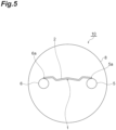
- FIGS. 2 to 5 are a perspective view, a front view, a side view, and a top view schematically illustrating an internal structure of the emitter illustrated in FIG. 1 .
- the electron source 1 is fixed to an apex portion of the arch-shaped filament 2 at a contact 1a.
- the electron source 1 is a tip of an electron emission material.
- an electron emission material include high-melting point metals such as tungsten, tantalum, and hafnium, and oxides, carbides, and nitrides thereof; rare earth borides such as lanthanum boride (LaB 6 ) and cerium boride (CeB 6 ); and noble metal-rare earth alloys such as iridium cerium. From the viewpoint of electron emission characteristics, strength, and machinability, it is preferable that the electron source 1 be a single crystal tungsten tip having an axis orientation of ⁇ 100> orientation.
- a source supplying zirconium and oxygen (refer to Fig. 1 of Patent Literature 1) is applied to a part on a surface of the tip.
- a ZrO layer covering the surface of the tip is continuously formed. Accordingly, rise in the work function of the tip is curbed, and therefore the function as a thermal field radiation cathode is maintained for a long period of time.
- the filament 2 is for heating the electron source 1 by means of electrification.
- the filament 2 is attached between the pair of terminals 5 and 6 in an arch shape.
- the material of the filament 2 be a high-melting point metal having a melting point of 2,200°C or higher. Specific examples thereof include tungsten and alloys of tungsten and a high-melting point metal (for example, rhenium). Tungsten doped with an alkali metal (for example, potassium) for composition stabilization may be used.
- both ends of the arch-shaped filament 2 are respectively bonded to the terminals 5 and 6 and the electron source 1 is bonded to the apex portion of the filament 2, there is an advantage that bonding work can be efficiently performed compared to when a filament is constituted using two wires. That is, when one arch-shaped filament is used, a manufacturing step can become simpler than when end portions of two wires on one side are respectively bonded to a pair of terminals and an electron source is bonded to end portions thereof on the other side.
- both end portions of the filament 2 are bonded to the front side (the right side in FIG. 4 ) of the pair of terminals 5 and 6.
- a contact 5a is a location where one end portion of the filament 2 is bonded to a side surface of the terminal 5.
- a contact 6a is a location where the other end portion of the filament 2 is bonded to a side surface of the terminal 6 (refer to Fig. 3 ).
- the contact 1a is a location where the electron source 1 and the filament 2 are bonded to each other.
- a pair of bent portions 3a and 3b and a pair of bent portions 4a and 4b are formed in the filament 2 according to the present embodiment. Since the filament 2 has a plurality of bent portions, stress due to thermal deformation is relaxed, and thus displacement of the electron source 1 can be curbed.
- the pair of bent portions 3a and 3b are simultaneously formed by folding a machined filament having an arch shape, and the same applies to the pair of bent portions 4a and 4b as well.
- the bent portions 3a and 4a are provided between the contact 5a and the contact 1a.
- the bent portion 3b and 4b are provided between the contact 6a and the contact 1a.
- a bending angle in the bent portions 3a and 3b (the angle ⁇ in FIG. 4 ) is 10° to 40°, for example, and it may be 15° to 30°.
- a bending angle (the angle ⁇ in FIG. 4 ) in the bent portions 4a and 4b is also 10° to 40°, for example, and it may also be 15° to 30°.
- this angle is 10° or larger, second parts 2b, which are necessary to provide a shift distance D (the distance D illustrated in FIG. 4 , which will be described below) to a certain extent or longer, tend to be able to be shortened.
- the angle is 40° or smaller, folding tends to be easily performed.
- the filament 2 has first parts 2a extending upward from the contact 5a with respect to the terminal 5, the second parts 2b bent from the first parts 2a and extending obliquely upward, and third parts 2c bent from the second parts 2b and extending upward.
- the electron source 1 can be disposed at the center position between the pair of terminals 5 and 6 when viewed from above (refer to Fig. 5 ).
- the third parts 2c to which the electron source 1 is bonded extend upward, there is also an advantage that work of fixing the electron source 1 is easily performed.
- the angle ⁇ and the angle ⁇ illustrated in FIG. 4 are practically the same, the extending direction of the first parts 2a and the extending direction of the third parts 2c can coincide with each other. These extending directions coincide with the irradiation direction of an electron beam, and it is preferable to coincide with the extending direction of the needle-shaped electron source 1 as well.
- the position of the contact 1a between the filament 2 and the electron source 1 be shifted from the position of the contact 5a between the terminal 5 and the filament 2 by 100 ⁇ m or longer in a horizontal direction (the leftward direction in FIG. 4 ). Accordingly, when the emitter 10 is viewed from above, the electron source 1 can be disposed at the center position between the pair of terminals 5 and 6.
- This shift distance (the distance D illustrated in FIG. 4 ) may be set in accordance with the thicknesses of the terminals 5 and 6 and the electron source 1.
- the shift distance D may be 100 to 700 ⁇ m or 400 to 600 ⁇ m.
- the electron source 1 is bonded to the rear side (the left side in FIG. 4 ) of the filament 2
- the electron source 1 may be bonded to the front side (the right side in FIG. 4 ) of the filament 2.
- the present invention is not limited to the foregoing embodiment.
- a thermal field emission-type emitter has been described, but a form according to the foregoing embodiment may also be applied to a field emission-type emitter.
- a field emission-type emitter does not require the suppressor 9 illustrated in FIG. 1 .
- a single crystal tungsten tip having an axis orientation of ⁇ 310> orientation is used as an electron source.
- An emitter 20 illustrated in FIG. 6 is provided with a filament 12 having the pair of bent portions 3a and 3b.
- the filament 12 When viewed from a side, the filament 12 has a first part 12a extending upward from the contact 5a, and a second part 12b bent from the first part 12a and extending obliquely upward, and the electron source 1 is fixed to the apex portion of the second part 12b.
- the second part 12b is inclined to the center side (the left side in FIG. 6 ) of the terminal 5.
- the emitter 10 is provided with one filament 2
- the emitter may be provided with a plurality of filaments, may have a structure in which one electron source is fixed to each of a plurality of filaments, or may have a structure in which one electron source is fixed by a plurality of filaments.
- FIGS. 1 to 5 were produced using the foregoing materials.
- FIG. 7 to 10 are SEM photographs of the filament according to Example 1.
- FIG. 7 illustrates the filament in its entirety.
- FIG. 8 illustrates a shape when the filament is viewed from the front.
- FIG. 9 illustrates a shape when the filament is viewed from a side.
- FIG. 10 illustrates a shape when the filament is viewed from above.
- the emitter according to Example 1 was produced by the following procedure. First, two pairs of bent portions were formed in an arch-shaped filament. Both the bent portions had a bending angle of 20°. Thereafter, end portions of the filament were bonded to a pair of terminals by welding. Further, an electron source was bonded to the apex portion of the filament by welding. As illustrated in FIG. 9 , the end portions of the filament were respectively bonded to the front side (the right side in FIG. 9 ) of the pair of terminals, and the electron source was bonded to the rear side (the left side in FIG. 9 ) of the filament.
- An emitter having the constitution illustrated in FIG. 6 was produced in a manner similar to that of Example 1 except that a pair of bent portions (the bending angle: 20°) were formed in place of two pairs of bent portions (the bending angle: 20°) formed in the filament.
- An emitter having the constitution illustrated in FIG. 11 was produced in a manner similar to that of Example 1 except that no bent portions were provided in the filament.
- An emitter 30 illustrated in FIG. 11 is provided with an arch-shaped filament 13 in which no bent portions were formed.
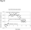
- FIGS. 12 to 14 shows the results.
- Electron source 1a: Contact, 2, 12: Filament, 2a: First part, 2b: Second part, 2c: Third part, 5, 6: Terminal, 3a, 3b, 3a, 3b: Bent portion, 5a, 6a: Contact, 8: Insulator, 9: Suppressor, 9a: Hole, 10, 20: Emitter, 12a: First part, 12b: Second part, 13: Filament (comparative example), 30: Emitter (comparative example), ⁇ , ⁇ : Bending angle, D: Shift distance
Landscapes
- Chemical & Material Sciences (AREA)
- Analytical Chemistry (AREA)
- Electron Sources, Ion Sources (AREA)
- Cold Cathode And The Manufacture (AREA)
- Solid Thermionic Cathode (AREA)
Abstract
Description
- The present disclosure relates to an emitter and a device provided with the same.
- An emitter is a device emitting an electron beam and is mounted in an electron microscope and a semiconductor inspection device, for example. A thermal field emission emitter is known as a form of an emitter. This emitter is provided with an insulator, a pair of terminals, an arch-shaped filament, and an electron source fixed to the filament.
Patent Literature 1 discloses an invention relating to a thermal field radiation cathode used in electron microscopes, electron beam exposing machines, and the like.FIG. 2 of this literature illustrates a thermal field radiation cathode provided with atungsten tip 1, a tungsten wire 3, aninsulator 4, and a pair ofmetal struts 5. FIG. 7A ofPatent Literature 2 also illustrates an emitter having a similar constitution. -
- [Patent Literature 1]
Japanese Unexamined Patent Publication No. H6-76731 - [Patent Literature 2]
Japanese Unexamined Patent Publication No. 2003-331714 - Since a filament provided in a thermal field emission emitter is heated to approximately 1,800 K at the time of operation, an electron source may be displaced due to thermal deformation of the filament. Excessive displacement of the electron source results in the following problems. That is, even if the coaxiality of an electron source with respect to a hole of a suppressor electrode or a hole of an extracting electrode provided in an emitter has been adjusted before heating, when the electron source is excessively displaced due to heating, they are deprived of the coaxiality. Accordingly, there is concern over an adverse influence on electron emission characteristics, and an irradiation direction and an irradiation position of an electron beam.
- The present disclosure provides an emitter in which deviation of an irradiation direction and an irradiation position of an electron beam caused by displacement of an electron source is sufficiently small, and a device provided with the same.
- An emitter according to an aspect of the present disclosure includes an insulator, a pair of terminals attached to the insulator separately from each other, at least one filament attached between the pair of terminals in an arch shape, and an electron source fixed to the filament. The filament has bent portions between a contact with respect to the electron source and contacts with respect to the terminals. Since the filament has the bent portions, stress due to thermal deformation is relaxed, and thus displacement of the electron source can be curbed.
- It is preferable that when the emitter is viewed from a side in a state where the pair of terminals are positioned below and the emitter is disposed in a direction in which the electron source is positioned above the pair of terminals, the filament have at least first parts extending upward from the contacts with respect to the terminals, second parts bent from the first parts and extending obliquely upward, and third parts bent from the second parts and extending upward. Since the third parts extend upward, there is an advantage that the electron source is easily fixed to the third parts.
- It is preferable that when the emitter disposed in a direction similar to that above is viewed from a side, a position of a contact between the filament and the electron source be shifted from positions of contacts between the terminals and the filament by 100 µm or longer in a horizontal direction. By employing this constitution, when the emitter is viewed from above, the electron source can be disposed at a center position between the pair of terminals.
- In the present disclosure, for example, a material of the electron source is one kind of material selected from the group consisting of rare earth borides; high-melting point metals, and oxides, carbides, and nitrides thereof; and noble metal-rare earth alloys.
- A device according to another aspect of the present disclosure is provided with the foregoing emitter. Examples of a device to be provided with the emitter include electron microscopes, semiconductor manufacturing devices, inspection devices, and machining devices.
- According to the present disclosure, an emitter in which deviation of an irradiation direction and an irradiation position of an electron beam caused by displacement of an electron source is sufficiently small, and a device provided with the same are provided.
-
-
FIG. 1 is a partial cross-sectional view schematically illustrating an embodiment of an emitter according to the present disclosure. -
FIG. 2 is a perspective view schematically illustrating an internal structure of the emitter illustrated inFIG. 1 . -
FIG. 3 is a front view of the internal structure illustrated inFIG. 2 . -
FIG. 4 is a side view of the internal structure illustrated inFIG. 2 . -
FIG. 5 is a top view of the internal structure illustrated inFIG. 2 . -
FIG. 6 is a side view schematically illustrating the internal structure of the emitter according to another embodiment of the present disclosure. -
FIG. 7 is an SEM photograph of a filament according to Example 1. -
FIG. 8 is an SEM photograph of the filament according to Example 1. -
FIG. 9 is an SEM photograph of the filament according to Example 1. -
FIG. 10 is an SEM photograph of the filament according to Example 1. -
FIG. 11 is a side view schematically illustrating a constitution of the emitter according to Comparative Example 1. -
FIG. 12 is a graph showing an amount of displacement of an electron source of the emitter according to Example 1. -
FIG. 13 is a graph showing an amount of displacement of the electron source of the emitter according to Example 2. -
FIG. 14 is a graph showing an amount of displacement of the electron source of the emitter according to Comparative Example 1. - Hereinafter, an embodiment of the present disclosure will be described in detail with reference to the drawings. In the following description, the same reference signs are applied to parts which are the same or corresponding, and duplicate description thereof will be omitted. In addition, unless otherwise stated, positional relationships such as up, down, left, right, and the like are based on the positional relationships illustrated in the drawings. The dimensional ratios in drawings are not limited to the illustrated ratios. When terms such as "left", "right", "front", "rear", "up", "down", "upward", and "downward" are utilized in description of this specification and the claims, these are intended for description and do not always permanently mean these relative positions.
-
FIG. 1 is a partial cross-sectional view schematically illustrating an emitter according to the present embodiment. Anemitter 10 illustrated in this diagram is referred to as a thermal field emission type. Examples of a device provided with theemitter 10 include an electron microscope, a semiconductor manufacturing device, an inspection device, and a machining device. Theemitter 10 is provided with anelectron source 1, an arch-shaped filament 2, a pair ofterminals insulator 8, and asuppressor 9. Theelectron source 1 is heated by means of electrification with respect to thefilament 2, and an electron beam is emitted from a tip portion of theelectron source 1. Ahole 9a is provided on an upper surface of thesuppressor 9, which is disposed such that theelectron source 1 protrudes through thehole 9a. From the viewpoint of electron emission characteristics and the like, it is preferable that coaxiality with respect to thehole 9a be maintained in theelectron source 1 before and after electrification.FIGS. 2 to 5 are a perspective view, a front view, a side view, and a top view schematically illustrating an internal structure of the emitter illustrated inFIG. 1 . - The
electron source 1 is fixed to an apex portion of the arch-shaped filament 2 at acontact 1a. Theelectron source 1 is a tip of an electron emission material. Examples of an electron emission material include high-melting point metals such as tungsten, tantalum, and hafnium, and oxides, carbides, and nitrides thereof; rare earth borides such as lanthanum boride (LaB6) and cerium boride (CeB6); and noble metal-rare earth alloys such as iridium cerium. From the viewpoint of electron emission characteristics, strength, and machinability, it is preferable that theelectron source 1 be a single crystal tungsten tip having an axis orientation of <100> orientation. In this case, a source supplying zirconium and oxygen (refer toFig. 1 of Patent Literature 1) is applied to a part on a surface of the tip. By continuously supplying zirconium and oxygen to the surface of the tip from the supply source, a ZrO layer covering the surface of the tip is continuously formed. Accordingly, rise in the work function of the tip is curbed, and therefore the function as a thermal field radiation cathode is maintained for a long period of time. - The
filament 2 is for heating theelectron source 1 by means of electrification. Thefilament 2 is attached between the pair ofterminals filament 2 be a high-melting point metal having a melting point of 2,200°C or higher. Specific examples thereof include tungsten and alloys of tungsten and a high-melting point metal (for example, rhenium). Tungsten doped with an alkali metal (for example, potassium) for composition stabilization may be used. When both ends of the arch-shapedfilament 2 are respectively bonded to theterminals electron source 1 is bonded to the apex portion of thefilament 2, there is an advantage that bonding work can be efficiently performed compared to when a filament is constituted using two wires. That is, when one arch-shaped filament is used, a manufacturing step can become simpler than when end portions of two wires on one side are respectively bonded to a pair of terminals and an electron source is bonded to end portions thereof on the other side. - When the emitter is viewed from a side, both end portions of the
filament 2 are bonded to the front side (the right side inFIG. 4 ) of the pair ofterminals contact 5a is a location where one end portion of thefilament 2 is bonded to a side surface of theterminal 5. Acontact 6a is a location where the other end portion of thefilament 2 is bonded to a side surface of the terminal 6 (refer toFig. 3 ). Thecontact 1a is a location where theelectron source 1 and thefilament 2 are bonded to each other. - As illustrated in
FIG. 2 , a pair ofbent portions bent portions 4a and 4b are formed in thefilament 2 according to the present embodiment. Since thefilament 2 has a plurality of bent portions, stress due to thermal deformation is relaxed, and thus displacement of theelectron source 1 can be curbed. For example, the pair ofbent portions bent portions 4a and 4b as well. Thebent portions contact 5a and thecontact 1a. Thebent portion 3b and 4b are provided between thecontact 6a and thecontact 1a. - A bending angle in the
bent portions FIG. 4 ) is 10° to 40°, for example, and it may be 15° to 30°. A bending angle (the angle β inFIG. 4 ) in thebent portions 4a and 4b is also 10° to 40°, for example, and it may also be 15° to 30°. When this angle is 10° or larger,second parts 2b, which are necessary to provide a shift distance D (the distance D illustrated inFIG. 4 , which will be described below) to a certain extent or longer, tend to be able to be shortened. On the other hand, when the angle is 40° or smaller, folding tends to be easily performed. - As illustrated in
FIG. 4 , when theemitter 10 is viewed from a side (in a direction in which theterminal 6 on the other side is hidden by theterminal 5 on one side and cannot be seen), thefilament 2 hasfirst parts 2a extending upward from thecontact 5a with respect to theterminal 5, thesecond parts 2b bent from thefirst parts 2a and extending obliquely upward, andthird parts 2c bent from thesecond parts 2b and extending upward. When viewed from a side, since thesecond parts 2b are inclined to the center side (the left side inFIG. 4 ) of theterminal 5, theelectron source 1 can be disposed at the center position between the pair ofterminals Fig. 5 ). In addition, since thethird parts 2c to which theelectron source 1 is bonded extend upward, there is also an advantage that work of fixing theelectron source 1 is easily performed. When the angle α and the angle β illustrated inFIG. 4 are practically the same, the extending direction of thefirst parts 2a and the extending direction of thethird parts 2c can coincide with each other. These extending directions coincide with the irradiation direction of an electron beam, and it is preferable to coincide with the extending direction of the needle-shapedelectron source 1 as well. - When the
emitter 10 is viewed from a side, it is preferable that the position of thecontact 1a between thefilament 2 and theelectron source 1 be shifted from the position of thecontact 5a between the terminal 5 and thefilament 2 by 100 µm or longer in a horizontal direction (the leftward direction inFIG. 4 ). Accordingly, when theemitter 10 is viewed from above, theelectron source 1 can be disposed at the center position between the pair ofterminals FIG. 4 ) may be set in accordance with the thicknesses of theterminals electron source 1. The shift distance D may be 100 to 700 µm or 400 to 600 µm. In the present embodiment, a form in which theelectron source 1 is bonded to the rear side (the left side inFIG. 4 ) of thefilament 2 has been described as an example. However, when a sufficiently long shift distance D can be set, theelectron source 1 may be bonded to the front side (the right side inFIG. 4 ) of thefilament 2. - Hereinabove, the embodiment of the present disclosure has been described, but the present invention is not limited to the foregoing embodiment. For example, in the foregoing embodiment, a thermal field emission-type emitter has been described, but a form according to the foregoing embodiment may also be applied to a field emission-type emitter. A field emission-type emitter does not require the
suppressor 9 illustrated inFIG. 1 . In addition, for example, a single crystal tungsten tip having an axis orientation of <310> orientation is used as an electron source. - In the foregoing embodiment, a case in which the
filament 2 has two pairs of bent portions has been described as an example, but the filament may have a pair of bent portions or three or more pairs of bent portions. Anemitter 20 illustrated inFIG. 6 is provided with afilament 12 having the pair ofbent portions filament 12 has afirst part 12a extending upward from thecontact 5a, and asecond part 12b bent from thefirst part 12a and extending obliquely upward, and theelectron source 1 is fixed to the apex portion of thesecond part 12b. When viewed from a side, thesecond part 12b is inclined to the center side (the left side inFIG. 6 ) of theterminal 5. In addition, in the foregoing embodiment, a case in which theemitter 10 is provided with onefilament 2 has been described as an example. However, the emitter may be provided with a plurality of filaments, may have a structure in which one electron source is fixed to each of a plurality of filaments, or may have a structure in which one electron source is fixed by a plurality of filaments. - Hereinafter, the present disclosure will be described on the basis of examples and a comparative example. The present invention is not limited to the following examples.
- The following materials were prepared.
- Electron source: single crystal tungsten tip (diameter: 0.1 mm, length: 1.2 mm, axis orientation of <100>)
- Filament: tungsten-rhenium filament (diameter: 0.1 mm, length: 14 mm)
- Emitters having constitutions illustrated in
FIGS. 1 to 5 were produced using the foregoing materials.FIG. 7 to 10 are SEM photographs of the filament according to Example 1.FIG. 7 illustrates the filament in its entirety.FIG. 8 illustrates a shape when the filament is viewed from the front.FIG. 9 illustrates a shape when the filament is viewed from a side.FIG. 10 illustrates a shape when the filament is viewed from above. - The emitter according to Example 1 was produced by the following procedure. First, two pairs of bent portions were formed in an arch-shaped filament. Both the bent portions had a bending angle of 20°. Thereafter, end portions of the filament were bonded to a pair of terminals by welding. Further, an electron source was bonded to the apex portion of the filament by welding. As illustrated in
FIG. 9 , the end portions of the filament were respectively bonded to the front side (the right side inFIG. 9 ) of the pair of terminals, and the electron source was bonded to the rear side (the left side inFIG. 9 ) of the filament. - An emitter having the constitution illustrated in
FIG. 6 was produced in a manner similar to that of Example 1 except that a pair of bent portions (the bending angle: 20°) were formed in place of two pairs of bent portions (the bending angle: 20°) formed in the filament. - An emitter having the constitution illustrated in
FIG. 11 was produced in a manner similar to that of Example 1 except that no bent portions were provided in the filament. Anemitter 30 illustrated inFIG. 11 is provided with an arch-shapedfilament 13 in which no bent portions were formed. - Amounts of displacement of the electron source when the filaments of the respective emitters according to the examples and the comparative example were electrified and heated were measured. The device and the conditions for the measurement are as follows.
FIGS. 12 to 14 shows the results. - Measurement device: laser displacement meter (manufactured by KEYENCE CORPORATION, product name: multi-color laser displacement meter CL-3000)
- Electrification time: 5 to 15 minutes
- Current value: 1.54 A
- Voltage: 1.6 V
- Displacement direction: lateral direction in
FIGS. 4 ,6 , and11 - The results of Examples 1 and 2 and Comparative Example 1 indicate that displacement of the electron source due to electrification can be reduced by providing bent portions in the filament.
- 1: Electron source, 1a: Contact, 2, 12: Filament, 2a: First part, 2b: Second part, 2c: Third part, 5, 6: Terminal, 3a, 3b, 3a, 3b: Bent portion, 5a, 6a: Contact, 8: Insulator, 9: Suppressor, 9a: Hole, 10, 20: Emitter, 12a: First part, 12b: Second part, 13: Filament (comparative example), 30: Emitter (comparative example), α, β: Bending angle, D: Shift distance
Claims (5)
- An emitter comprising:an insulator;a pair of terminals attached to the insulator separately from each other;at least one filament attached between the pair of terminals in an arch shape; andan electron source fixed to the filament,wherein the filament has bent portions between a contact with respect to the electron source and contacts with respect to the terminals.
- The emitter according to claim 1,
wherein when the emitter is viewed from a side in a state where the pair of terminals are positioned below and the emitter is disposed in a direction in which the electron source is positioned above the pair of terminals, the filament has at least first parts extending upward from the contacts with respect to the terminals, second parts bent from the first parts and extending obliquely upward, and third parts bent from the second parts and extending upward. - The emitter according to claim 1 or 2,
wherein when the emitter is viewed from a side in a state where the pair of terminals are positioned below and the emitter is disposed in a direction in which the electron source is positioned above the pair of terminals, a position of a contact between the filament and the electron source is shifted from positions of contacts between the terminals and the filament by 100 µm or longer in a horizontal direction. - The emitter according to any one of claims 1 to 3,
wherein a material of the electron source is one kind of material selected from the group consisting of rare earth borides; high-melting point metals, and oxides, carbides, and nitrides thereof; and noble metal-rare earth alloys. - A device comprising the emitter according to any one of claims 1 to 4.
Applications Claiming Priority (2)
| Application Number | Priority Date | Filing Date | Title |
|---|---|---|---|
| JP2021046160 | 2021-03-19 | ||
| PCT/JP2022/010356 WO2022196499A1 (en) | 2021-03-19 | 2022-03-09 | Emitter and device provided with same |
Publications (3)
| Publication Number | Publication Date |
|---|---|
| EP4303906A1 true EP4303906A1 (en) | 2024-01-10 |
| EP4303906A4 EP4303906A4 (en) | 2024-05-22 |
| EP4303906B1 EP4303906B1 (en) | 2025-01-29 |
Family
ID=83320540
Family Applications (1)
| Application Number | Title | Priority Date | Filing Date |
|---|---|---|---|
| EP22771250.2A Active EP4303906B1 (en) | 2021-03-19 | 2022-03-09 | Emitter and device provided with same |
Country Status (6)
| Country | Link |
|---|---|
| US (1) | US12125663B2 (en) |
| EP (1) | EP4303906B1 (en) |
| JP (1) | JP7523668B2 (en) |
| CN (1) | CN116325061A (en) |
| TW (1) | TW202244972A (en) |
| WO (1) | WO2022196499A1 (en) |
Family Cites Families (20)
| Publication number | Priority date | Publication date | Assignee | Title |
|---|---|---|---|---|
| US3631291A (en) * | 1969-04-30 | 1971-12-28 | Gen Electric | Field emission cathode with metallic boride coating |
| NL7605820A (en) | 1976-05-31 | 1977-12-02 | Philips Nv | ELECTRON BEAM TUBE WITH FIELD EMISSION ELECTRONIC SOURCE, FIELD EMISSION ELECTRONIC SOURCE FOR SUCH ELECTRONIC BEAM TUBE AND METHOD FOR MANUFACTURE OF SUCH FIELD EMISSION ELECTRONIC SOURCE. |
| JPS6016060B2 (en) | 1981-11-06 | 1985-04-23 | 株式会社日立製作所 | Cathode manufacturing method |
| US4427886A (en) * | 1982-08-02 | 1984-01-24 | Wisconsin Alumni Research Foundation | Low voltage field emission electron gun |
| JPH03165432A (en) | 1989-11-22 | 1991-07-17 | Jeol Ltd | Field emission type electron gun |
| JP3260204B2 (en) | 1992-06-24 | 2002-02-25 | 電気化学工業株式会社 | Thermal field emission cathode |
| JP3641936B2 (en) * | 1998-05-29 | 2005-04-27 | ウシオ電機株式会社 | Electron beam tube |
| UA28130C2 (en) | 1998-11-09 | 2000-10-16 | Товариство З Обмеженою Відповідальністю "Нікос-Еко" | Straight filament cathode pack for electron-beam tubes |
| US6798126B2 (en) | 2002-05-03 | 2004-09-28 | Fei Company | High angular intensity Schottky electron point source |
| JP2008091307A (en) * | 2006-09-05 | 2008-04-17 | Denki Kagaku Kogyo Kk | Electron source |
| JP4782736B2 (en) | 2007-07-12 | 2011-09-28 | 電気化学工業株式会社 | Electron source |
| WO2009044564A1 (en) * | 2007-10-05 | 2009-04-09 | Denki Kagaku Kogyo Kabushiki Kaisha | Electron source and electron beam device |
| JP2010287415A (en) | 2009-06-11 | 2010-12-24 | Nissin Ion Equipment Co Ltd | Filament and ion source equipped therewith |
| CN102576635B (en) | 2009-10-08 | 2015-03-04 | 株式会社爱发科 | Filament for electron gun and method for producing same |
| US8896195B2 (en) * | 2010-10-21 | 2014-11-25 | Hermes Microvision, Inc. | Filament for electron source |
| US8736170B1 (en) * | 2011-02-22 | 2014-05-27 | Fei Company | Stable cold field emission electron source |
| US9847208B1 (en) * | 2016-08-10 | 2017-12-19 | ICT Integrated Circuit Testing Gesellschaft für Halbleiterprüftechnik mbH | Electron beam device, cold field emitter, and method for regeneration of a cold field emitter |
| WO2019008738A1 (en) * | 2017-07-07 | 2019-01-10 | 株式会社日立ハイテクノロジーズ | Field emission-type electron source and charged particle beam device |
| KR102120946B1 (en) * | 2018-11-16 | 2020-06-10 | (주)엠크래프츠 | Electron microscope with automatic beam alignment |
| EP3920206B1 (en) | 2019-01-30 | 2023-08-09 | National Institute for Materials Science | Emitter, electron gun using same, and electronic device |
-
2022
- 2022-03-09 WO PCT/JP2022/010356 patent/WO2022196499A1/en not_active Ceased
- 2022-03-09 JP JP2023507032A patent/JP7523668B2/en active Active
- 2022-03-09 US US18/550,077 patent/US12125663B2/en active Active
- 2022-03-09 EP EP22771250.2A patent/EP4303906B1/en active Active
- 2022-03-09 CN CN202280006822.3A patent/CN116325061A/en active Pending
- 2022-03-11 TW TW111108932A patent/TW202244972A/en unknown
Also Published As
| Publication number | Publication date |
|---|---|
| CN116325061A (en) | 2023-06-23 |
| US20240153730A1 (en) | 2024-05-09 |
| WO2022196499A1 (en) | 2022-09-22 |
| TW202244972A (en) | 2022-11-16 |
| EP4303906A4 (en) | 2024-05-22 |
| US12125663B2 (en) | 2024-10-22 |
| EP4303906B1 (en) | 2025-01-29 |
| JPWO2022196499A1 (en) | 2022-09-22 |
| JP7523668B2 (en) | 2024-07-26 |
Similar Documents
| Publication | Publication Date | Title |
|---|---|---|
| US6464551B1 (en) | Filament design, method, and support structure | |
| EP2175472B1 (en) | Electron source | |
| US8223923B2 (en) | X-ray source with metal wire cathode | |
| EP1256123B1 (en) | Low input power schottky emitter | |
| US8548124B2 (en) | Electron source and cathode cup thereof | |
| US12125663B2 (en) | Emitter and device provided with same | |
| US11915921B2 (en) | Electron source, method for manufacturing same, emitter, and device including same | |
| EP1129464A1 (en) | Direct heating cathode unit and electron gun using the same | |
| AU2002214294B2 (en) | Gas discharge tube | |
| JP2005259606A (en) | Thermionic emission filament | |
| EP4734145A1 (en) | Emitter | |
| EP4734146A1 (en) | Emitter | |
| JP2024121384A (en) | Emitter | |
| JP7640787B2 (en) | Electron source and manufacturing method thereof, emitter and device including same | |
| EP4379767A1 (en) | Electron source, manufacturing method therefor, and device comprising electron source | |
| EP4503087A1 (en) | Emitter and device comprising same | |
| JP2019204721A (en) | Electron beam source in mass spectrometer | |
| JP2024121498A (en) | Emitter | |
| TW202541083A (en) | Emitter | |
| TW202601707A (en) | Emitter | |
| JPH1167114A (en) | Plasma generator and ion implanter | |
| JPH04248233A (en) | Cathode body structure for x-ray tube | |
| KR20020081914A (en) | Field emission cathode | |
| JPH01264131A (en) | Cathode body structure |
Legal Events
| Date | Code | Title | Description |
|---|---|---|---|
| STAA | Information on the status of an ep patent application or granted ep patent |
Free format text: STATUS: THE INTERNATIONAL PUBLICATION HAS BEEN MADE |
|
| PUAI | Public reference made under article 153(3) epc to a published international application that has entered the european phase |
Free format text: ORIGINAL CODE: 0009012 |
|
| STAA | Information on the status of an ep patent application or granted ep patent |
Free format text: STATUS: REQUEST FOR EXAMINATION WAS MADE |
|
| 17P | Request for examination filed |
Effective date: 20231005 |
|
| AK | Designated contracting states |
Kind code of ref document: A1 Designated state(s): AL AT BE BG CH CY CZ DE DK EE ES FI FR GB GR HR HU IE IS IT LI LT LU LV MC MK MT NL NO PL PT RO RS SE SI SK SM TR |
|
| REG | Reference to a national code |
Ref country code: DE Ref legal event code: R079 Free format text: PREVIOUS MAIN CLASS: H01J0037060000 Ipc: H01J0037065000 Ref country code: DE Ref legal event code: R079 Ref document number: 602022010271 Country of ref document: DE Free format text: PREVIOUS MAIN CLASS: H01J0037060000 Ipc: H01J0037065000 |
|
| A4 | Supplementary search report drawn up and despatched |
Effective date: 20240418 |
|
| RIC1 | Information provided on ipc code assigned before grant |
Ipc: H01J 1/22 20060101ALI20240412BHEP Ipc: H01J 37/07 20060101ALI20240412BHEP Ipc: H01J 37/065 20060101AFI20240412BHEP |
|
| DAV | Request for validation of the european patent (deleted) | ||
| DAX | Request for extension of the european patent (deleted) | ||
| GRAP | Despatch of communication of intention to grant a patent |
Free format text: ORIGINAL CODE: EPIDOSNIGR1 |
|
| STAA | Information on the status of an ep patent application or granted ep patent |
Free format text: STATUS: GRANT OF PATENT IS INTENDED |
|
| INTG | Intention to grant announced |
Effective date: 20240926 |
|
| GRAS | Grant fee paid |
Free format text: ORIGINAL CODE: EPIDOSNIGR3 |
|
| GRAA | (expected) grant |
Free format text: ORIGINAL CODE: 0009210 |
|
| STAA | Information on the status of an ep patent application or granted ep patent |
Free format text: STATUS: THE PATENT HAS BEEN GRANTED |
|
| AK | Designated contracting states |
Kind code of ref document: B1 Designated state(s): AL AT BE BG CH CY CZ DE DK EE ES FI FR GB GR HR HU IE IS IT LI LT LU LV MC MK MT NL NO PL PT RO RS SE SI SK SM TR |
|
| REG | Reference to a national code |
Ref country code: GB Ref legal event code: FG4D |
|
| REG | Reference to a national code |
Ref country code: CH Ref legal event code: EP |
|
| P01 | Opt-out of the competence of the unified patent court (upc) registered |
Free format text: CASE NUMBER: APP_1488/2025 Effective date: 20250109 |
|
| REG | Reference to a national code |
Ref country code: DE Ref legal event code: R096 Ref document number: 602022010271 Country of ref document: DE |
|
| REG | Reference to a national code |
Ref country code: IE Ref legal event code: FG4D |
|
| PGFP | Annual fee paid to national office [announced via postgrant information from national office to epo] |
Ref country code: DE Payment date: 20250318 Year of fee payment: 4 |
|
| PGFP | Annual fee paid to national office [announced via postgrant information from national office to epo] |
Ref country code: AT Payment date: 20250417 Year of fee payment: 4 |
|
| PGFP | Annual fee paid to national office [announced via postgrant information from national office to epo] |
Ref country code: CZ Payment date: 20250203 Year of fee payment: 4 |
|
| REG | Reference to a national code |
Ref country code: NL Ref legal event code: MP Effective date: 20250129 |
|
| PG25 | Lapsed in a contracting state [announced via postgrant information from national office to epo] |
Ref country code: NL Free format text: LAPSE BECAUSE OF FAILURE TO SUBMIT A TRANSLATION OF THE DESCRIPTION OR TO PAY THE FEE WITHIN THE PRESCRIBED TIME-LIMIT Effective date: 20250129 |
|
| PG25 | Lapsed in a contracting state [announced via postgrant information from national office to epo] |
Ref country code: RS Free format text: LAPSE BECAUSE OF FAILURE TO SUBMIT A TRANSLATION OF THE DESCRIPTION OR TO PAY THE FEE WITHIN THE PRESCRIBED TIME-LIMIT Effective date: 20250429 |
|
| PG25 | Lapsed in a contracting state [announced via postgrant information from national office to epo] |
Ref country code: FI Free format text: LAPSE BECAUSE OF FAILURE TO SUBMIT A TRANSLATION OF THE DESCRIPTION OR TO PAY THE FEE WITHIN THE PRESCRIBED TIME-LIMIT Effective date: 20250129 |
|
| PG25 | Lapsed in a contracting state [announced via postgrant information from national office to epo] |
Ref country code: PL Free format text: LAPSE BECAUSE OF FAILURE TO SUBMIT A TRANSLATION OF THE DESCRIPTION OR TO PAY THE FEE WITHIN THE PRESCRIBED TIME-LIMIT Effective date: 20250129 |
|
| PG25 | Lapsed in a contracting state [announced via postgrant information from national office to epo] |
Ref country code: ES Free format text: LAPSE BECAUSE OF FAILURE TO SUBMIT A TRANSLATION OF THE DESCRIPTION OR TO PAY THE FEE WITHIN THE PRESCRIBED TIME-LIMIT Effective date: 20250129 |
|
| REG | Reference to a national code |
Ref country code: LT Ref legal event code: MG9D |
|
| PG25 | Lapsed in a contracting state [announced via postgrant information from national office to epo] |
Ref country code: NO Free format text: LAPSE BECAUSE OF FAILURE TO SUBMIT A TRANSLATION OF THE DESCRIPTION OR TO PAY THE FEE WITHIN THE PRESCRIBED TIME-LIMIT Effective date: 20250429 Ref country code: IS Free format text: LAPSE BECAUSE OF FAILURE TO SUBMIT A TRANSLATION OF THE DESCRIPTION OR TO PAY THE FEE WITHIN THE PRESCRIBED TIME-LIMIT Effective date: 20250529 |
|
| REG | Reference to a national code |
Ref country code: AT Ref legal event code: MK05 Ref document number: 1764332 Country of ref document: AT Kind code of ref document: T Effective date: 20250129 |
|
| PG25 | Lapsed in a contracting state [announced via postgrant information from national office to epo] |
Ref country code: HR Free format text: LAPSE BECAUSE OF FAILURE TO SUBMIT A TRANSLATION OF THE DESCRIPTION OR TO PAY THE FEE WITHIN THE PRESCRIBED TIME-LIMIT Effective date: 20250129 |
|
| PG25 | Lapsed in a contracting state [announced via postgrant information from national office to epo] |
Ref country code: LV Free format text: LAPSE BECAUSE OF FAILURE TO SUBMIT A TRANSLATION OF THE DESCRIPTION OR TO PAY THE FEE WITHIN THE PRESCRIBED TIME-LIMIT Effective date: 20250129 Ref country code: PT Free format text: LAPSE BECAUSE OF FAILURE TO SUBMIT A TRANSLATION OF THE DESCRIPTION OR TO PAY THE FEE WITHIN THE PRESCRIBED TIME-LIMIT Effective date: 20250529 |
|
| PG25 | Lapsed in a contracting state [announced via postgrant information from national office to epo] |
Ref country code: BG Free format text: LAPSE BECAUSE OF FAILURE TO SUBMIT A TRANSLATION OF THE DESCRIPTION OR TO PAY THE FEE WITHIN THE PRESCRIBED TIME-LIMIT Effective date: 20250129 Ref country code: GR Free format text: LAPSE BECAUSE OF FAILURE TO SUBMIT A TRANSLATION OF THE DESCRIPTION OR TO PAY THE FEE WITHIN THE PRESCRIBED TIME-LIMIT Effective date: 20250430 |
|
| PG25 | Lapsed in a contracting state [announced via postgrant information from national office to epo] |
Ref country code: AT Free format text: LAPSE BECAUSE OF FAILURE TO SUBMIT A TRANSLATION OF THE DESCRIPTION OR TO PAY THE FEE WITHIN THE PRESCRIBED TIME-LIMIT Effective date: 20250129 |
|
| PG25 | Lapsed in a contracting state [announced via postgrant information from national office to epo] |
Ref country code: SE Free format text: LAPSE BECAUSE OF FAILURE TO SUBMIT A TRANSLATION OF THE DESCRIPTION OR TO PAY THE FEE WITHIN THE PRESCRIBED TIME-LIMIT Effective date: 20250129 |
|
| PG25 | Lapsed in a contracting state [announced via postgrant information from national office to epo] |
Ref country code: SM Free format text: LAPSE BECAUSE OF FAILURE TO SUBMIT A TRANSLATION OF THE DESCRIPTION OR TO PAY THE FEE WITHIN THE PRESCRIBED TIME-LIMIT Effective date: 20250129 |
|
| PG25 | Lapsed in a contracting state [announced via postgrant information from national office to epo] |
Ref country code: DK Free format text: LAPSE BECAUSE OF FAILURE TO SUBMIT A TRANSLATION OF THE DESCRIPTION OR TO PAY THE FEE WITHIN THE PRESCRIBED TIME-LIMIT Effective date: 20250129 |
|
| PG25 | Lapsed in a contracting state [announced via postgrant information from national office to epo] |
Ref country code: MC Free format text: LAPSE BECAUSE OF FAILURE TO SUBMIT A TRANSLATION OF THE DESCRIPTION OR TO PAY THE FEE WITHIN THE PRESCRIBED TIME-LIMIT Effective date: 20250129 |
|
| PG25 | Lapsed in a contracting state [announced via postgrant information from national office to epo] |
Ref country code: IT Free format text: LAPSE BECAUSE OF FAILURE TO SUBMIT A TRANSLATION OF THE DESCRIPTION OR TO PAY THE FEE WITHIN THE PRESCRIBED TIME-LIMIT Effective date: 20250129 |
|
| PG25 | Lapsed in a contracting state [announced via postgrant information from national office to epo] |
Ref country code: EE Free format text: LAPSE BECAUSE OF FAILURE TO SUBMIT A TRANSLATION OF THE DESCRIPTION OR TO PAY THE FEE WITHIN THE PRESCRIBED TIME-LIMIT Effective date: 20250129 |
|
| PG25 | Lapsed in a contracting state [announced via postgrant information from national office to epo] |
Ref country code: RO Free format text: LAPSE BECAUSE OF FAILURE TO SUBMIT A TRANSLATION OF THE DESCRIPTION OR TO PAY THE FEE WITHIN THE PRESCRIBED TIME-LIMIT Effective date: 20250129 |
|
| REG | Reference to a national code |
Ref country code: CH Ref legal event code: H13 Free format text: ST27 STATUS EVENT CODE: U-0-0-H10-H13 (AS PROVIDED BY THE NATIONAL OFFICE) Effective date: 20251023 |
|
| PG25 | Lapsed in a contracting state [announced via postgrant information from national office to epo] |
Ref country code: SK Free format text: LAPSE BECAUSE OF FAILURE TO SUBMIT A TRANSLATION OF THE DESCRIPTION OR TO PAY THE FEE WITHIN THE PRESCRIBED TIME-LIMIT Effective date: 20250129 |
|
| REG | Reference to a national code |
Ref country code: DE Ref legal event code: R097 Ref document number: 602022010271 Country of ref document: DE |
|
| PG25 | Lapsed in a contracting state [announced via postgrant information from national office to epo] |
Ref country code: LU Free format text: LAPSE BECAUSE OF NON-PAYMENT OF DUE FEES Effective date: 20250309 |
|
| PLBE | No opposition filed within time limit |
Free format text: ORIGINAL CODE: 0009261 |
|
| STAA | Information on the status of an ep patent application or granted ep patent |
Free format text: STATUS: NO OPPOSITION FILED WITHIN TIME LIMIT |
|
| REG | Reference to a national code |
Ref country code: BE Ref legal event code: MM Effective date: 20250331 |
|
| 26N | No opposition filed |
Effective date: 20251030 |
|
| PG25 | Lapsed in a contracting state [announced via postgrant information from national office to epo] |
Ref country code: FR Free format text: LAPSE BECAUSE OF NON-PAYMENT OF DUE FEES Effective date: 20250329 |
|
| PG25 | Lapsed in a contracting state [announced via postgrant information from national office to epo] |
Ref country code: BE Free format text: LAPSE BECAUSE OF NON-PAYMENT OF DUE FEES Effective date: 20250331 |
|
| PG25 | Lapsed in a contracting state [announced via postgrant information from national office to epo] |
Ref country code: CH Free format text: LAPSE BECAUSE OF NON-PAYMENT OF DUE FEES Effective date: 20250331 |
|
| PG25 | Lapsed in a contracting state [announced via postgrant information from national office to epo] |
Ref country code: IE Free format text: LAPSE BECAUSE OF NON-PAYMENT OF DUE FEES Effective date: 20250309 |